


 Loading...
STMicroelectronics NUCLEO-F411RE, NUCLEO-F030R8, NUCLEO-F401RE, NUCLEO-F303RE, NUCLEO-F070RB User guide
...UM1724
User manual
STM32 Nucleo-64 boards
Introduction
The STM32 Nucleo-64 board (NUCLEO-F030R8, NUCLEO-F070RB, NUCLEO-F072RB, NUCLEO-F091RC, NUCLEO-F103RB, NUCLEO-F302R8, NUCLEO-F303RE, NUCLEO-F334R8, NUCLEO-F401RE, NUCLEO-F410RB, NUCLEO-F411RE, NUCLEO-F446RE, NUCLEO-L053R8, NUCLEO-L073RZ, NUCLEO-L152RE, NUCLEO-L476RG) provides an affordable and flexible way for users to try out new ideas and build prototypes with the STM32 microcontrollers in LQFP64 package, choosing from the various combinations of performance, power consumption and features. The Arduino™ connectivity support and ST Morpho headers make it easy to expand the functionality of the Nucleo open development platform with a wide choice of specialized shields. The STM32 Nucleo board does not require any separate probe as it integrates the ST-LINK/V2-1 debugger/programmer. The STM32 Nucleo board comes with the STM32 comprehensive software HAL library together with various packaged software examples, as well as direct access to mbed online resources at http://mbed.org/.
Figure 1. STM32 Nucleo-64 board (1)
1. Picture not contractual.
August 2015 |
DocID025833 Rev 9 |
1/61 |
www.st.com

Content |
UM1724 |
|
|
Content
1 |
Ordering information . . . . . . . . . . . . . . . . . . . . . . . . . . . . . . . . . . . . |
. . . . 2 |
||
2 |
Conventions |
. . . . . . . . . . . . . . . . . . . . . . . . . . . . . . . . . . . . . . . . . . . . |
. . . 3 |
|
3 |
Quick start . |
. . . . . . . . . . . . . . . . . . . . . . . . . . . . . . . . . . . . . . . . . . . . . |
. . . 4 |
|
|
3.1 |
Getting started . . . . . . . . . . . . . . . . . . . . . . . . . . . . . . . . . . . . . . . . . . . |
. . . 4 |
|
|
3.2 |
System requirements . . . . . . . . . . . . . . . . . . . . . . . . . . . . . . . . . . . . . . |
. . . 4 |
|
|
3.3 |
NUCLEO-L476RG bootloader limitations . . . . . . . . . . . . . . . . . . . . . . . |
. . . 4 |
|
4 |
Features . . . . |
. . . . . . . . . . . . . . . . . . . . . . . . . . . . . . . . . . . . . . . . . . . . |
. . . 6 |
|
|
4.1 |
Hardware configuration variants . . . . . . . . . . . . . . . . . . . . . . . . . . . . . . |
. . . 6 |
|
5 |
Hardware layout and configuration . . . . . . . . . . . . . . . . . . . . . . . . . . |
. . . 7 |
||
|
5.1 |
Cuttable PCB . . . . . . . . . . . . . . . . . . . . . . . . . . . . . . . . . . . . . . . . . . . . |
. . . 9 |
|
|
5.2 |
Embedded ST-LINK/V2-1 . . . . . . . . . . . . . . . . . . . . . . . . . . . . . . . . . . . |
. . 10 |
|
|
|
5.2.1 |
Driver . . . . . . . . . . . . . . . . . . . . . . . . . . . . . . . . . . . . . . . . . . . . . . . |
. . . 11 |
|
|
5.2.2 |
ST-LINK/V2-1 firmware upgrade . . . . . . . . . . . . . . . . . . . . . . . . . . . |
. . . 11 |
|
|
5.2.3 |
Using the ST-LINK/V2-1 to program/debug the STM32 on board |
. . . . 12 |
5.2.4Using ST-LINK/V2-1 to program/debug an external STM32 application 12
5.3 Power supply and power selection . . . . . . . . . . . . . . . . . . . . . . . . . . . . . . 13
5.3.1 |
Power supply input from the USB connector . . . . . . . . . . . . . . . . . . . . . |
13 |
5.3.2 |
External power supply inputs: VIN and EV5 . . . . . . . . . . . . . . . . . . . . . |
14 |
5.3.3 |
External power supply input: + 3V3 . . . . . . . . . . . . . . . . . . . . . . . . . . . . |
17 |
5.3.4 |
External power supply output . . . . . . . . . . . . . . . . . . . . . . . . . . . . . . . . |
17 |
5.4 LEDs . . . . . . . . . . . . . . . . . . . . . . . . . . . . . . . . . . . . . . . . . . . . . . . . . . . . 17 5.5 Push buttons . . . . . . . . . . . . . . . . . . . . . . . . . . . . . . . . . . . . . . . . . . . . . . 18 5.6 JP6 (IDD) . . . . . . . . . . . . . . . . . . . . . . . . . . . . . . . . . . . . . . . . . . . . . . . . . 18
5.6.1 |
OSC clock supply . . . . . . . . . . . . . . . . . . . . . . . . . . . . . . . . . . . . . . . . . |
18 |
5.6.2 |
OSC 32 kHz clock supply . . . . . . . . . . . . . . . . . . . . . . . . . . . . . . . . . . . |
19 |
5.7 USART communication . . . . . . . . . . . . . . . . . . . . . . . . . . . . . . . . . . . . . . 20 5.8 Solder bridges . . . . . . . . . . . . . . . . . . . . . . . . . . . . . . . . . . . . . . . . . . . . . 20 5.9 Extension connectors . . . . . . . . . . . . . . . . . . . . . . . . . . . . . . . . . . . . . . . . 22 5.10 Arduino connectors . . . . . . . . . . . . . . . . . . . . . . . . . . . . . . . . . . . . . . . . . 30
1/61 |
DocID025833 Rev 9 |

UM1724 |
|
Content |
|
5.11 STMicroelectronics Morpho connector . . . . . . . . . . . . . . . . . . . . . . . |
. . . . 44 |
6 |
Mechanical drawing . . . . . . . . . . . . . . . . . . . . . . . . . . . . . . . . . . . . . |
. . . 53 |
7 |
Electrical schematics . . . . . . . . . . . . . . . . . . . . . . . . . . . . . . . . . . . . |
. . . 54 |
8 |
References . . . . . . . . . . . . . . . . . . . . . . . . . . . . . . . . . . . . . . . . . . . . . |
. . . 58 |
9 |
Revision history . . . . . . . . . . . . . . . . . . . . . . . . . . . . . . . . . . . . . . . . |
. . . 59 |
DocID025833 Rev 9 |
2/61 |

List of Tables |
UM1724 |
|
|
List of Tables
Table 1. Ordering information . . . . . . . . . . . . . . . . . . . . . . . . . . . . . . . . . . . . . . . . . . . . . . . . . . . . . . . 2 Table 2. ON/OFF conventions . . . . . . . . . . . . . . . . . . . . . . . . . . . . . . . . . . . . . . . . . . . . . . . . . . . . . . 3 Table 3. Jumper states . . . . . . . . . . . . . . . . . . . . . . . . . . . . . . . . . . . . . . . . . . . . . . . . . . . . . . . . . . . 10 Table 4. Debug connector CN4 (SWD) . . . . . . . . . . . . . . . . . . . . . . . . . . . . . . . . . . . . . . . . . . . . . . 12 Table 5. JP1 configuration table . . . . . . . . . . . . . . . . . . . . . . . . . . . . . . . . . . . . . . . . . . . . . . . . . . . . 14 Table 6. External power sources . . . . . . . . . . . . . . . . . . . . . . . . . . . . . . . . . . . . . . . . . . . . . . . . . . . 15 Table 7. Power-related jumper . . . . . . . . . . . . . . . . . . . . . . . . . . . . . . . . . . . . . . . . . . . . . . . . . . . . . 15 Table 8. +3.3V eternal power source . . . . . . . . . . . . . . . . . . . . . . . . . . . . . . . . . . . . . . . . . . . . . . . . 17 Table 9. Solder bridges. . . . . . . . . . . . . . . . . . . . . . . . . . . . . . . . . . . . . . . . . . . . . . . . . . . . . . . . . . . 20 Table 10. Arduino connectors on
NUCLEO-F030R8, NUCLEO-F070RB, NUCLEO-F072RB, NUCLEO-F091RC. . . . . . . . . 30 Table 11. Arduino connectors on NUCLEO-F103RB . . . . . . . . . . . . . . . . . . . . . . . . . . . . . . . . . . . . . 31 Table 12. Arduino connectors on NUCLEO-F302R8 . . . . . . . . . . . . . . . . . . . . . . . . . . . . . . . . . . . . . 33 Table 13. Arduino connectors on NUCLEO-F303RE . . . . . . . . . . . . . . . . . . . . . . . . . . . . . . . . . . . . . 34 Table 14. Arduino connectors on NUCLEO-F334R8 . . . . . . . . . . . . . . . . . . . . . . . . . . . . . . . . . . . . . 35 Table 15. Arduino connectors on NUCLEO-F401RE, NUCLEO-F411RE . . . . . . . . . . . . . . . . . . . . . 36 Table 16. Arduino connectors on NUCLEO-L053R8 . . . . . . . . . . . . . . . . . . . . . . . . . . . . . . . . . . . . . 37 Table 17. Arduino connectors on NUCLEO-L073RZ . . . . . . . . . . . . . . . . . . . . . . . . . . . . . . . . . . . . . 38 Table 18. Arduino connectors on NUCLEO-F446RE . . . . . . . . . . . . . . . . . . . . . . . . . . . . . . . . . . . . . 40 Table 19. Arduino connectors on NUCLEO-F410RB . . . . . . . . . . . . . . . . . . . . . . . . . . . . . . . . . . . . . 41 Table 20. Arduino connectors on NUCLEO-L152RE . . . . . . . . . . . . . . . . . . . . . . . . . . . . . . . . . . . . . 42 Table 21. Arduino connectors on NUCLEO-L476RG . . . . . . . . . . . . . . . . . . . . . . . . . . . . . . . . . . . . . 43 Table 22. STMicroelectronics Morpho connector on NUCLEO-F030R8 . . . . . . . . . . . . . . . . . . . . . . 44 Table 23. STMicroelectronics Morpho connector on NUCLEO-F070RB . . . . . . . . . . . . . . . . . . . . . . 45 Table 24. STMicroelectronics Morpho connector on
NUCLEO-F072RB, NUCLEO-F091RC, NUCLEO-F303RE, NUCLEO-F334R8. . . . . . . . . 46 Table 25. STMicroelectronics Morpho connector on NUCLEO-F103RB . . . . . . . . . . . . . . . . . . . . . . 47 Table 26. STMicroelectronics Morpho connector on NUCLEO-F302R8 . . . . . . . . . . . . . . . . . . . . . . 48 Table 27. STMicroelectronics Morpho connector on NUCLEO-F401RE,
NUCLEO-F411RE,NUCLEO-F446RE . . . . . . . . . . . . . . . . . . . . . . . . . . . . . . . . . . . . . . . . 49 Table 28. STMicroelectronics Morpho connector on
NUCLEO-L053R8, NUCLEO-L073RZ, NUCLEO-L152RE. . . . . . . . . . . . . . . . . . . . . . . . . 50 Table 29. STMicroelectronics Morpho connector on NUCLEO-L476RG . . . . . . . . . . . . . . . . . . . . . . 51 Table 30. STMicroelectronics Morpho connector on NUCLEO-F410RB . . . . . . . . . . . . . . . . . . . . . . 52 Table 31. Document revision history . . . . . . . . . . . . . . . . . . . . . . . . . . . . . . . . . . . . . . . . . . . . . . . . . 59
1/61 |
DocID025833 Rev 9 |

UM1724 |
List of Figures |
|
|
List of Figures
Figure 1. STM32 Nucleo-64 board (1) . . . . . . . . . . . . . . . . . . . . . . . . . . . . . . . . . . . . . . . . . . . . . . . . . 1 Figure 1. Hardware block diagram . . . . . . . . . . . . . . . . . . . . . . . . . . . . . . . . . . . . . . . . . . . . . . . . . . . 7 Figure 2. Top layout . . . . . . . . . . . . . . . . . . . . . . . . . . . . . . . . . . . . . . . . . . . . . . . . . . . . . . . . . . . . . . . 8 Figure 3. Bottom layout . . . . . . . . . . . . . . . . . . . . . . . . . . . . . . . . . . . . . . . . . . . . . . . . . . . . . . . . . . . . 9 Figure 4. Typical configuration. . . . . . . . . . . . . . . . . . . . . . . . . . . . . . . . . . . . . . . . . . . . . . . . . . . . . . 11 Figure 5. Updating the list of drivers in Device Manager . . . . . . . . . . . . . . . . . . . . . . . . . . . . . . . . . . 11 Figure 6. Connecting the STM32 Nucleo board to program the on-board STM32 . . . . . . . . . . . . . . 12 Figure 7. Using ST-LINK/V2-1 to program the STM32 on an external application . . . . . . . . . . . . . . 13 Figure 8. NUCLEO-F030R8. . . . . . . . . . . . . . . . . . . . . . . . . . . . . . . . . . . . . . . . . . . . . . . . . . . . . . . . 22 Figure 9. NUCLEO-F070RB . . . . . . . . . . . . . . . . . . . . . . . . . . . . . . . . . . . . . . . . . . . . . . . . . . . . . . . 22 Figure 10. NUCLEO-F072RB . . . . . . . . . . . . . . . . . . . . . . . . . . . . . . . . . . . . . . . . . . . . . . . . . . . . . . . 23 Figure 11. NUCLEO-F091RC . . . . . . . . . . . . . . . . . . . . . . . . . . . . . . . . . . . . . . . . . . . . . . . . . . . . . . . 23 Figure 12. NUCLEO-F103RB . . . . . . . . . . . . . . . . . . . . . . . . . . . . . . . . . . . . . . . . . . . . . . . . . . . . . . . 24 Figure 13. NUCLEO-F302R8. . . . . . . . . . . . . . . . . . . . . . . . . . . . . . . . . . . . . . . . . . . . . . . . . . . . . . . . 24 Figure 14. NUCLEO-F303RE . . . . . . . . . . . . . . . . . . . . . . . . . . . . . . . . . . . . . . . . . . . . . . . . . . . . . . . 25 Figure 15. NUCLEO-F334R8. . . . . . . . . . . . . . . . . . . . . . . . . . . . . . . . . . . . . . . . . . . . . . . . . . . . . . . . 25 Figure 16. NUCLEO-F401RE . . . . . . . . . . . . . . . . . . . . . . . . . . . . . . . . . . . . . . . . . . . . . . . . . . . . . . . 26 Figure 17. NUCLEO-F411RE . . . . . . . . . . . . . . . . . . . . . . . . . . . . . . . . . . . . . . . . . . . . . . . . . . . . . . . 26 Figure 18. NUCLEO-L053R8 . . . . . . . . . . . . . . . . . . . . . . . . . . . . . . . . . . . . . . . . . . . . . . . . . . . . . . . . 27 Figure 19. NUCLEO-L073RZ. . . . . . . . . . . . . . . . . . . . . . . . . . . . . . . . . . . . . . . . . . . . . . . . . . . . . . . . 27 Figure 20. NUCLEO-L152RE. . . . . . . . . . . . . . . . . . . . . . . . . . . . . . . . . . . . . . . . . . . . . . . . . . . . . . . . 28 Figure 21. NUCLEO-L476RG . . . . . . . . . . . . . . . . . . . . . . . . . . . . . . . . . . . . . . . . . . . . . . . . . . . . . . . 28 Figure 22. NUCLEO-F446RE . . . . . . . . . . . . . . . . . . . . . . . . . . . . . . . . . . . . . . . . . . . . . . . . . . . . . . . 29 Figure 23. NUCLEO-F410RB . . . . . . . . . . . . . . . . . . . . . . . . . . . . . . . . . . . . . . . . . . . . . . . . . . . . . . . 29 Figure 24. STM32 Nucleo board mechanical drawing . . . . . . . . . . . . . . . . . . . . . . . . . . . . . . . . . . . . . 53 Figure 25. Electrical schematics (1/4) . . . . . . . . . . . . . . . . . . . . . . . . . . . . . . . . . . . . . . . . . . . . . . . . . 54 Figure 26. Electrical schematics (2/4) . . . . . . . . . . . . . . . . . . . . . . . . . . . . . . . . . . . . . . . . . . . . . . . . . 55 Figure 27. Electrical schematics (3/4) . . . . . . . . . . . . . . . . . . . . . . . . . . . . . . . . . . . . . . . . . . . . . . . . . 56 Figure 28. Electrical schematics (4/4) . . . . . . . . . . . . . . . . . . . . . . . . . . . . . . . . . . . . . . . . . . . . . . . . . 57
DocID025833 Rev 9 |
1/61 |

Ordering information |
UM1724 |
|
|
1 Ordering information
Table 1 lists the order codes and the respective targeted MCU.
|
Table 1. Ordering information |
|
Order code |
|
Targeted MCU |
|
|
|
NUCLEO-F030R8 |
|
STM32F030R8T6 |
|
|
|
NUCLEO-F070RB |
|
STM32F070RBT6 |
|
|
|
NUCLEO-F072RB |
|
STM32F072RBT6 |
|
|
|
NUCLEO-F091RC |
|
STM32F091RCT6 |
|
|
|
NUCLEO-F103RB |
|
STM32F103RBT6 |
|
|
|
NUCLEO-F302R8 |
|
STM32F302R8T6 |
|
|
|
NUCLEO-F303RE |
|
STM32F303RET6 |
|
|
|
NUCLEO-F334R8 |
|
STM32F334R8T6 |
|
|
|
NUCLEO-F401RE |
|
STM32F401RET6 |
|
|
|
NUCLEO-F410RB |
|
STM32F410RBT6 |
|
|
|
NUCLEO-F411RE |
|
STM32F411RET6 |
|
|
|
NUCLEO-F446RE |
|
STM32F446RET6 |
|
|
|
NUCLEO-L053R8 |
|
STM32L053R8T6 |
|
|
|
NUCLEO-L073RZ |
|
STM32L073RZT6 |
|
|
|
NUCLEO-L152RE |
|
STM32L152RET6 |
|
|
|
NUCLEO-L476RG |
|
STM32L476RGT6 |
|
|
|
The meaning of NUCLEO-TXXXRY codification is as follows:
•TXXX describes the STM32 MCU product line
•R describes the pin count (R for 64 pins)
•Y describes the code size (8 for 64K, B for 128K, C for 256K, E for 512K, G for 1MB, Z for 192K)
The order code is printed on a sticker placed at the top or bottom side of the board.
2/61 |
DocID025833 Rev 9 |

UM1724 |
Conventions |
|
|
2 Conventions
Table 2 provides the conventions used for the ON and OFF settings in the present document.
|
Table 2. ON/OFF conventions |
Convention |
Definition |
|
|
Jumper JP1 ON |
Jumper fitted |
|
|
Jumper JP1 OFF |
Jumper not fitted |
|
|
Solder bridge SBx ON |
SBx connections closed by solder or 0 ohm resistor |
|
|
Solder bridge SBx OFF |
SBx connections left open |
|
|
We refer to “STM32 Nucleo board” and “STM32 Nucleo boards” in this document for all information that is common to all sale types.
DocID025833 Rev 9 |
3/61 |

Quick start |
UM1724 |
|
|
3 Quick start
The STM32 Nucleo board is a low-cost and easy-to-use development platform used to quickly evaluate and start a development with an STM32 microcontroller in LQFP64 package.
Before installing and using the product, please accept the Evaluation Product License Agreement from www.st.com/epla.
For more information on the STM32 Nucleo boards and to access the demonstration software, visit www.st.com/stm32nucleo.
3.1Getting started
Follow the sequence below to configure the STM32 Nucleo board and launch the demo software:
1.Check the jumper position on the board, JP1 off, JP5 (PWR) on U5V, JP6 on (IDD), CN2 on (NUCLEO) selected.
2.For correct identification of all device interfaces from the host PC, install the Nucleo USB driver available on www.st.com/stm32nucleo, prior to connecting the board
3.Connect the STM32 Nucleo board to a PC with a USB cable ‘type A to mini-B’ through USB connector CN1 to power the board. The red LED LD3 (PWR) and LD1 (COM) should light up. LD1 (COM) and green LED LD2 should blink.
4.Press button B1 (left button).
5.Observe how the blinking of the green LED LD2 changes according to clicks on button B1.
6.The demo software and several software examples on how use the STM32 Nucleo board features are available on www.st.com/stm32nucleo.
7.Develop the application using the available examples.
3.2System requirements
•Windows OS (XP, 7, 8)
•USB type A to Mini-B USB cable
3.3NUCLEO-L476RG bootloader limitations
Boot from system Flash memory results in executing bootloader code stored in the system Flash memory protected against write and erase. This allows in-system programming (ISP), that is, flashing the MCU user Flash memory. It also allows writing data into RAM. The data come in via one of communication interfaces such as USART, SPI, I²C bus, USB or CAN.
Bootloader version can be identified by reading Bootloader ID at the address 0x1FFF6FFE.
The STM32L476RGT6 part soldered on the NUCLEO-L476RG main board is marked with a date code corresponding to its date of manufacture. STM32L476RGT6 parts with the date code prior or equal to week 22 of 2015 are fitted with bootloader V 9.0 affected by the
4/61 |
DocID025833 Rev 9 |

UM1724 |
Quick start |
|
|
limitations to be worked around, as described hereunder. Parts with the date code starting from week 23 of 2015 contain bootloader V 9.2 in which the limitations no longer exist.
To locate the visual date code information on the STM32L476RGT6 package, refer to its datasheet (DS10198) available on www.st.com, section Package Information. Date code related portion of the package marking takes Y WW format, where Y is the last digit of the year and WW is the week. For example, a part manufactured in week 23 of 2015 bares the date code 5 23.
Bootloader ID of the bootloader V 9.0 is 0x90.
The following limitations exist in the bootloader V 9.0:
1.RAM data get corrupted when written via USART/SPI/I2C/USB interface
Description:
Data write operation into RAM space via USART, SPI, I²C bus or USB results in wrong or no data written.
Workaround:
To correct the issue of wrong write into RAM, download STSW-STM32158 bootloader V 9.0 patch package from www.st.com and load "Bootloader V9.0 SRAM patch" to the MCU, following the information in readme.txt file available in the package.
2.User Flash memory data get corrupted when written via CAN interface
Description:
Data write operation into user Flash memory space via CAN interface results in wrong or no data written.
Workaround:
To correct the issue of wrong write into Flash memory, download STSW-STM32158 bootloader V 0.9 patch package from www.st.com and load "Bootloader V9.0 CAN patch" to the MCU, following the information in readme.txt file available in the package
DocID025833 Rev 9 |
5/61 |

Features |
UM1724 |
|
|
4 Features
The STM32 Nucleo boards offer the following features:
•STM32 microcontroller with LQFP64 package
•Two types of extension resources
–Arduino Uno Revision 3 connectivity
–STMicroelectronics Morpho extension pin headers for full access to all STM32 I/Os
•mbed-enabled(a)
•On-board ST-LINK/V2-1 debugger/programmer with SWD connector
–selection-mode switch to use the kit as a standalone ST-LINK/V2-1
•Flexible board power supply
–USB VBUS
–External VIN (7V<VIN<12V) supply voltage from Arduino connectors or ST Morpho connector
–External 5V (E5V) supply voltage from ST Morpho connector
–External +3.3V supply voltage from Arduino connector or ST Morpho connector
•Three LEDs
–USB communication (LD1), user LED (LD2), power LED (LD3)
•Two push buttons: USER and RESET
•LSE crystal:
–32.768kHz crystal oscillator (depending on board version)
•USB re-enumeration capability: three different interfaces supported on USB
–Virtual Com port
–Mass storage
–Debug port
•Comprehensive free software HAL library including a variety of software examples
•Supported by wide choice of Integrated Development Environments (IDEs) including IAR, Keil, GCC-based IDEs
4.1Hardware configuration variants
The board can be delivered with different configurations of the oscillator of the target MCU. For all the details concerning High Speed oscillator configurations refer to Section 5.6.1. For all the details concerning Low speed oscillator configurations refer to Section 5.6.2.
a. See http://mbed.org/
6/61 |
DocID025833 Rev 9 |
UM1724 |
Hardware layout and configuration |
|
|
5 Hardware layout and configuration
The STM32 Nucleo board is designed around the STM32 microcontrollers in a 64-pin LQFP package.
Figure 1 shows the connections between the STM32 and its peripherals (ST-LINK/V2-1, pushbutton, LED, Arduino connectors and STMicroelectronics Morpho connector).
Figure 2 and Figure 3 show the location of these features on the STM32 Nucleo board.
Figure 1. Hardware block diagram
67 /,1. SDUW |
|
0LQL |
|
|
|
|
|
|
|
|
|
|
|
|
|
|
|
|
86% |
|
|
|
|
|
|
|
(PEHGGHG |
|
|
|
|
|
|
|
67 /,1. 9 |
|
|
|
|
|
<![if ! IE]> <![endif]>6:' |
|
|
|
|
|
|
|
% |
|
|
|
|
|
|
|
86(5 |
|
670 |
|
|
|
|
|
|
|
|
|
|
|
|
| <![if ! IE]> <![endif]>KHDGHUH[WHQVLRQ0RUSKR |
|
,2 |
0LFURFRQWUROOHU |
,2 |
|
|
<![if ! IE]> <![endif]>KHDGHUH[WHQVLRQ0RUSKR |
|
|
|
|
||||
| <![if ! IE]> <![endif]>FRQQHFWRU$UGXLQR |
,2 |
5(6(7 |
,2 |
|
<![if ! IE]> <![endif]>FRQQHFWRU$UGXLQR |
||
|
% |
|
/(' |
||||
|
5(6(7 |
|
/' |
||||
|
|
|
|
||||
0&8 SDUW |
|
|
|
|
|
|
|
|
|
|
|
|
|
|
06 9 |
|
|
DocID025833 Rev 9 |
|
|
|
7/61 |
|

Hardware layout and configuration |
UM1724 |
|
|
Figure 2. Top layout
|
&1 |
|
|
|
|
67 /,1. 1XFOHR |
||
VHOHFWRU
&1 6:' FRQQHFWRU
% 86(5 EXWWRQ
-3 ,'' PHDVXUHPHQW
/'5HG /('
SRZHU
&1$UGXLQR
FRQQHFWRU
&1
67 0RUSKR
FRQQHFWRU
&1
$UGXLQR
FRQQHFWRU
.+]FU\VWDO
&1 67 /,1. 86%
PLQL % FRQQHFWRU
/'  5HG *UHHQ /(' &20
% 5(6(7 EXWWRQ
6%9 UHJXODWRU RXWSXW
/'*UHHQ /('
&1 $UGXLQR FRQQHFWRU
&1
 67 0RUSKR FRQQHFWRU
&1 $UGXLQR FRQQHFWRU
8
670 PLFURFRQWUROOHU
06 9
1. Crystal may be present or not depending on board version, refer to Section 5.6.2
8/61 |
DocID025833 Rev 9 |
UM1724 |
Hardware layout and configuration |
||
|
|
|
|
|
|
Figure 3. Bottom layout |
|
4# 4# |
4# 4# 4# 4# |
4# 4# 4# 4# |
|
45 -*/, 64"35 |
3&4&37&% |
%&'"6-5 |
|
4# |
|
|
|
45 -*/, 480 |
|
|
|
|
|
|
6% |
4# |
|
67 /,1. |
|
|
5(6(7 |
||
45 -*/, .$0 |
|
|
|
|
|
|
6% |
|
|
|
86(5 EXWWRQ |
6% |
|
|
|
86(5 /(' |
|
|
|
6%
67 /,1. 0&2
.4 7
5.1Cuttable PCB
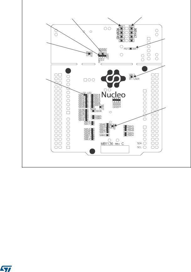
The STM32 Nucleo board is divided into two parts: ST-LINK part and target MCU part. The ST-LINK part of the PCB can be cut out to reduce the board size. In this case the remaining target MCU part can only be powered by VIN, E5V and 3.3V on STMicroelectronics Morpho connector CN7 or VIN and 3.3V on Arduino connector CN6. It is still possible to use the ST-LINK part to program the main MCU using wires between CN4 and SWD signals available on STMicroelectronics Morpho connector (SWCLK CN7 pin 15 and SWDIO CN7 pin 13).
DocID025833 Rev 9 |
9/61 |

Hardware layout and configuration |
UM1724 |
|
|
5.2Embedded ST-LINK/V2-1
The ST-LINK/V2-1 programming and debugging tool is integrated in the STM32 Nucleo boards.
The ST-LINK/V2-1 makes the STM32 Nucleo boards mbed enabled.
The embedded ST-LINK/V2-1 supports only SWD for STM32 devices. For information about debugging and programming features refer to UM1075 - ST-LINK/V2 in-circuit debugger/programmer for STM8 and STM32, User manual, which describes in detail all the ST-LINK/V2 features.
The changes versus ST-LINK/V2 version are listed below.
•New features supported on ST-LINK/V2-1:
–USB software re-enumeration
–Virtual com port interface on USB
–Mass storage interface on USB
–USB power management request for more than 100 mA power on USB
•Features not supported on ST-LINK/V2-1:
–SWIM interface
–Minimum supported application voltage limited to 3 V
•Known limitation:
–Activating the readout protection on ST-Link/V2-1 target prevents the target application from running afterwards. The target readout protection must be kept disabled on ST-Link/V2-1 boards.
There are two different ways to use the embedded ST-LINK/V2-1 depending on the jumper states (see Table 3 and Figure 4):
•Program/debug the MCU on board (Section 5.2.2),
•Program/debug an MCU in an external application board using a cable connected to SWD connector CN4 (Section 5.2.4).
|
Table 3. Jumper states |
|
Jumper state |
Description |
|
|
|
|
Both CN2 jumpers ON |
ST-LINK/V2-1 functions enabled for on board programming |
|
(default) |
||
|
||
|
|
|
Both CN2 jumpers OFF |
ST-LINK/V2-1 functions enabled for external CN4 connector |
|
(SWD supported) |
||
|
||
|
|
10/61 |
DocID025833 Rev 9 |
UM1724 |
Hardware layout and configuration |
|
|
Figure 4. Typical configuration
+DUGZDUH UHTXLUHPHQWV86% FDEOH W\SH $ WR PLQL %FRPSXWHU ZLWK :LQGRZV ;3
'HYHORSPHQW WRROFKDLQ
,$5 (:$50.HLO 0'. $50*&& EDVHG ,'(
06 9
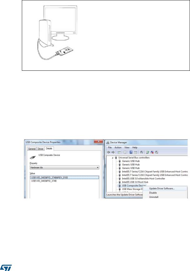
5.2.1Driver
|
The ST-LINK/V2-1 requires a dedicated USB driver, which can be found on www.st.com for |
|
Windows XP, 7, 8. |
|
In case the STM32 Nucleo board is connected to the PC before the driver is installed, some |
|
Nucleo interfaces may be declared as “Unknown” in the PC device manager. In this case |
|
the user must install the driver files (Figure 5), and from the device manager update the |
|
driver of the connected device. |
Note: |
Prefer using the “USB Composite Device” handle for a full recovery. |
|
Figure 5. Updating the list of drivers in Device Manager |
|
|
5.2.2ST-LINK/V2-1 firmware upgrade
The ST-LINK/V2-1 embeds a firmware upgrade mechanism for in-situ upgrade through the USB port. As the firmware may evolve during the life time of the ST-LINK/V2-1 product (for example new functionality, bug fixes, support for new microcontroller families), it is recommended to visit www.st.com before starting to use the STM32 Nucleo board and periodically, in order to stay up-to-date with the latest firmware version.
DocID025833 Rev 9 |
11/61 |
Hardware layout and configuration |
UM1724 |
|
|
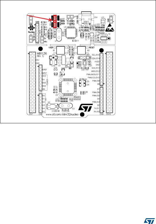
5.2.3Using the ST-LINK/V2-1 to program/debug the STM32 on board
To program the STM32 on the board, plug in the two jumpers on CN2, as shown in red in Figure 6. Do not use the CN4 connector as this could disturb the communication with the STM32 microcontroller of the STM32 Nucleo board.
Figure 6. Connecting the STM32 Nucleo board to program the on-board STM32
EϮ ũƵŵƉĞƌƐ KE
Eϰ ^t  ĐŽŶŶĞĐƚŽƌ
06 9
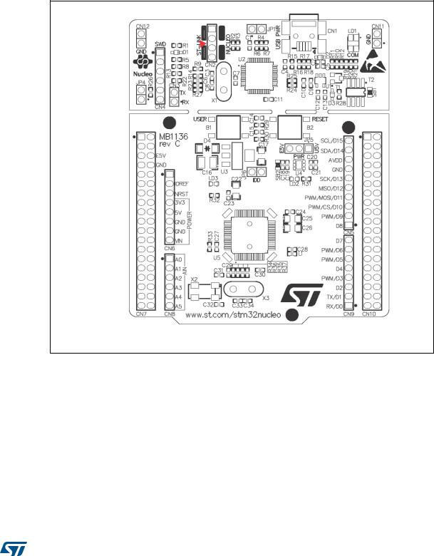
5.2.4Using ST-LINK/V2-1 to program/debug an external STM32 application
It is very easy to use the ST-LINK/V2-1 to program the STM32 on an external application. Simply remove the two jumpers from CN2 as illustrated in Figure 7, and connect the application to the CN4 debug connector according to Table 4.
Note: |
SB12 NRST (target MCU RESET) must be OFF if CN4 pin 5 is used in the external |
||||
|
application. |
|
|
|
|
|
|
Table 4. Debug connector CN4 (SWD) |
|
||
|
Pin |
|
CN4 |
|
Designation |
|
|
|
|
|
|
|
1 |
|
VDD_TARGET |
|
VDD from application |
|
|
|
|
|
|
|
2 |
|
SWCLK |
|
SWD clock |
|
|
|
|
|
|
|
3 |
|
GND |
|
Ground |
|
|
|
|
|
|
|
4 |
|
SWDIO |
|
SWD data input/output |
|
|
|
|
|
|
12/61 |
DocID025833 Rev 9 |
UM1724 |
|
|
Hardware layout and configuration |
||
|
|
|
|
|
|
|
|
Table 4. Debug connector CN4 (SWD) (continued) |
|||
|
5 |
|
NRST |
|
RESET of target MCU |
|
|
|
|
|
|
|
6 |
|
SWO |
|
Reserved |
|
|
|
|
|
|
Figure 7. Using ST-LINK/V2-1 to program the STM32 on an external application
$/ KVNQFST 0''
$/  48% DPOOFDUPS
.4 7
5.3Power supply and power selection
The power supply is provided either by the host PC through the USB cable, or by an external Source: VIN (7V-12V), E5V (5V) or +3V3 power supply pins on CN6 or CN7. In case VIN, E5V or +3V3 is used to power the Nucleo board, using an external power supply unit or an auxiliary equipment, this power source must comply with the standard EN-60950- 1: 2006+A11/2009, and must be Safety Extra Low Voltage (SELV) with limited power capability.
5.3.1Power supply input from the USB connector
The ST-LINK/V2-1 supports USB power management allowing to request more than 100 mA current to the host PC.
DocID025833 Rev 9 |
13/61 |

Hardware layout and configuration |
UM1724 |
|
|
All parts of the STM32 Nucleo board and shield can be powered from the ST-LINK USB connector CN1 (U5V or VBUS). Note that only the ST-LINK part is power supplied before the USB enumeration as the host PC only provides 100 mA to the board at that time. During the USB enumeration, the STM32 Nucleo board requires 300 mA of current to the Host PC. If the host is able to provide the required power, the targeted STM32 microcontroller is powered and the red LED LD3 is turned ON, thus the STM32 Nucleo board and its shield can consume a maximum of 300 mA current, not more. If the host is not able to provide the required current, the targeted STM32 microcontroller and the MCU part including the extension board are not power supplied. As a consequence the red LED LD3 remains turned OFF. In such case it is mandatory to use an external power supply as explained in the next chapter.
When the board is power supplied by USB (U5V) a jumper must be connected between pin 1 and pin 2 of JP5 as shown in Table 7.
JP1 is configured according to the maximum current consumption of the board when powered by USB (U5V). JP1 jumper can be set in case the board is powered by USB and maximum current consumption on U5V doesn’t exceed 100mA (including an eventual extension board or Arduino Shield). In such condition USB enumeration will always succeed since no more than 100mA is requested to the PC. Possible configurations of JP1 are summarized in Table 5.
Table 5. JP1 configuration table
Jumper state |
Power supply |
Allowed current |
|
|
|
|
|
JP1 jumper OFF |
USB power through CN1 |
300 mA max |
|
|
|
||
JP1 jumper ON |
100 mA max |
||
|
|||
|
|
|
|
Warning: If the maximum current consumption of the NUCLEO and its |
|
extension boards exceeds 300 mA, it is mandatory to power |
|
the NUCLEO using an external power supply connected to |
|
E5V or VIN. |
|
|
Note: |
In case the board is powered by an USB charger, there is no USB enumeration, so the led |
|
LD3 remains set to OFF permanently and the target MCU is not powered. In this specific |
|
case the jumper JP1 needs to be set to ON, to allow target MCU to be powered anyway. |
5.3.2 |
External power supply inputs: VIN and EV5 |
|
The external power sources VIN and EV5 are summarized in the Table 6. When the board is |
|
power supplied by VIN or E5V, the jumpers configuration must be the following: |
|
Jumper on JP5 pin 2 and pin 3 |
|
Jumper removed on JP1 |
14/61 |
DocID025833 Rev 9 |

UM1724 |
|
|
|
|
|
|
|
|
Hardware layout and configuration |
||||
|
|
|
|
|
|
|
|
|
|
|
|
|
|
|
|
|
|
|
Table 6. External power sources |
||||||||
|
Input power |
Connectors |
Voltage range |
|
Max |
|
|
|
|
Limitation |
|||
|
name |
|
pins |
|
current |
|
|
|
|
||||
|
|
|
|
|
|
|
|
|
|
|
|
|
|
|
|
|
|
|
|
|
|
|
From 7 V to 12 V only and input current capability |
||||
|
|
|
CN6 pin 8 |
|
|
|
|
|
is linked to input voltage: |
||||
|
VIN |
|
|
7 V to 12 V |
800 mA |
800 mA input current when Vin=7 V |
|||||||
|
|
CN7 pin 24 |
|
||||||||||
|
|
|
|
|
|
|
|
450 mA input current when 7 V<Vin (< or =) 9 V |
|||||
|
|
|
|
|
|
|
|
|
|||||
|
|
|
|
|
|
|
|
|
250 mA input current when 9 V<Vin (< or =) 12 V |
||||
|
|
|
|
|
|
|
|
|
|
|
|
|
|
|
E5V |
|
CN7 pin 6 |
4.75 V to 5.25 V |
500 mA |
- |
|||||||
|
|
|
|
|
|
|
|
|
|
|
|
|
|
|
|
|
|
|
Table 7. Power-related jumper |
||||||||
|
Jumper |
|
|
|
|
|
Description |
||||||
|
|
|
|
|
|
|
|
|
|
||||
|
|
|
U5V (ST-LINK VBUS) is used as power source when JP5 is set as shown below (Default |
||||||||||
|
|
|
|
|
|
|
|
setting) |
|||||
|
|
|
|
|
|
|
<![if ! IE]> <![endif]>(9 |
|
|
|
|
<![if ! IE]> <![endif]>89 |
|
|
|
|
|
|
|
|
|
|
|||||
|
|
|
|
|
|
|
|||||||
|
|
|
|
|
|
|
|
|
|
||||
|
JP5 |
|
|
|
|
|
|
|
|
|
|
|
|
|
|
|
|
|
|
|
|
|
|
|
|
|
|
|
|
|
VIN or E5V is used as power source when JP5 is set as shown below. |
||||||||||
|
|
|
|
||||||||||
|
|
|
|
|
|
|
|
|
|
|
|||
|
|
|
|
|
|
|
<![if ! IE]> <![endif]>(9 |
|
|
|
<![if ! IE]> <![endif]>89 |
|
|
|
|
|
|
|
|
|
|
|
|||||
|
|
|
|
|
|
|
|
|
|||||
|
|
|
|
|
|
|
|
|
|
|
|||
|
|
|
|
|
|
|
|
|
|
|
|
|
|
|
|
|
|
|
|
|
|
|
|
|
|
|
|
Using VIN or E5V as external power supply
VIN or E5V can be used as external power supply in case the current consumption of NUCLEO and extensions boards exceeds the allowed current on USB. In this condition it is still possible to use the USB for communication, for programming or debugging only, but it is mandatory to power supply the board first using VIN or E5V then connect the USB cable to the PC. Proceeding this way ensures that the enumeration occurs thanks to the external power source.
The following power sequence procedure must be respected:
1.Connect the jumper between pin 2 and pin 3 of JP5.
2.Check that JP1 is removed.
3.Connect the external power source to VIN or E5V.
4.Power on the external power supply 7 V< VIN < 12 V to VIN, or 5 V for E5V.
5.Check that LD3 is turned ON.
6.Connect the PC to USB connector CN1.
If this order is not respected, the board may be supplied by VBUS first then by VIN or E5V, and the following risks may be encountered:
DocID025833 Rev 9 |
15/61 |

Hardware layout and configuration |
UM1724 |
|
|
1.If more than 300 mA current is needed by the board, the PC may be damaged or the current supply can be limited by the PC. As a consequence the board is not powered correctly.
2.300 mA is requested at enumeration (since JP1 must be OFF) so there is risk that the request is rejected and the enumeration does not succeed if the PC cannot provide such current. Consequently the board is not power supplied (LED LD3 remains OFF).
16/61 |
DocID025833 Rev 9 |
Loading...