

Page 1
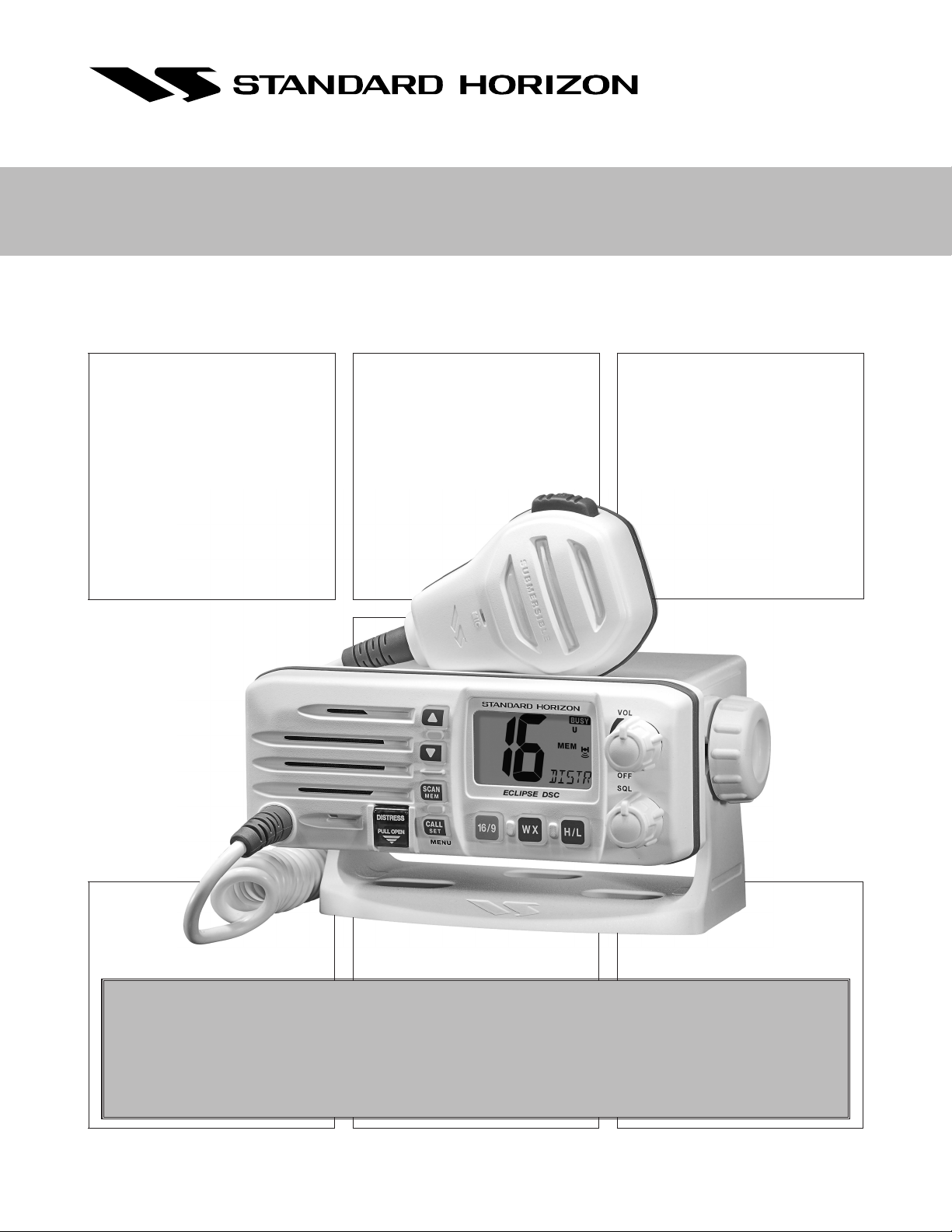
25 Watt VHF/FM DSC Marine Transceiver
ECLIPSE DSC GX1000SECLIPSE DSC GX1000S
ECLIPSE DSC GX1000S
ECLIPSE DSC GX1000SECLIPSE DSC GX1000S
SERVICE MANUAL
Important Note
This transceiver was assembled using Pb (lead) free solder, based on the RoHS specification.
Only lead-free solder (Alloy Composition: Sn-3.0Ag-0.5Cu) should be used for repairs performed on
this apparatus. The solder stated above utilizes the alloy composition required for compliance with the
lead-free specification, and any solder with the above alloy composition may be used.
EM030N90A
1
Page 2
Specifications
GENERAL
Channels: All USA, International and Canadian
Input Voltage: 13.8 VDC ±20%
Current Drain: Standby 0.3 A
Receive 1.0 A
Transmit 5.5 A (Hi); 1.5 A (Lo)
Individual DSC Directory Memory:15
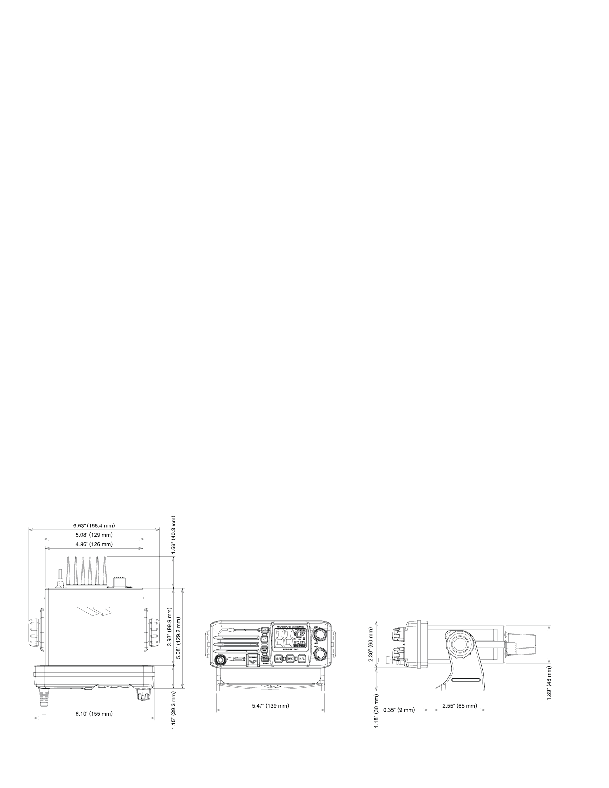
Dimensions: 2.4” H x 6.1” W x 6.7” D (60 H x 155 W x 170 D mm)
Flush-Mount Dimensions: 2.0” H x 5.2” W x 6.7” D (51 H x 131 W x 170 D mm)
Weight: 1.7 lbs (770 g)
TRANSMITTER
Frequency Range: 156.025 to 157.425 MHz
RF Output: 25 W (Hi); 1 W (Lo)
Conducted Spurious Emissions: 80 dB (Hi); 60 dB (Lo)
Audio Response: within +1/–3 of a 6 dB/octave pre-emphasis characteristic at 300 to 3000 Hz
Audio Distortion:5 %
Modulation: 16K0G3E, for DSC 16K0G2B
Frequency Stability (–20°C to +50°C): ±0.0005%
FM Hum and Noise: 50 dB
RECEIVER
Frequency Range: 156.050 to 163.275 MHz
Sensitivity: 12 dB SINAD 0.25 μV
Squelch Sensitivity (Threshold): 0.15 μV
Modulation Acceptance Bandwidth: ±7.5 kHz
Selectivity (TYP.): –70 dB (Spurious and Image Rejection)
–70 dB (Intermodulation and Rejection at 12 dB SINAD)
Audio Output: 4.5 W
Audio Response: within + 2/–8 of a 6 dB/octave de-emphasis characteristic at 300 to 3000 Hz
Frequency Stability (-20°C to +50°C): ±0.0005 %
Channel Spacing: 25 kHz
DSC Format: RTCM SC101
NMEA Input/Output: Output - DSC, DSE
Input - GLL, GGA, RMC and GNS
Performance specifications are nominal, unless otherwise indicated, and are subject to change without notice.
Measurements are made in accordance with EN301 025. All stated specifications are subject to change without notice or obligation.
2
Page 3
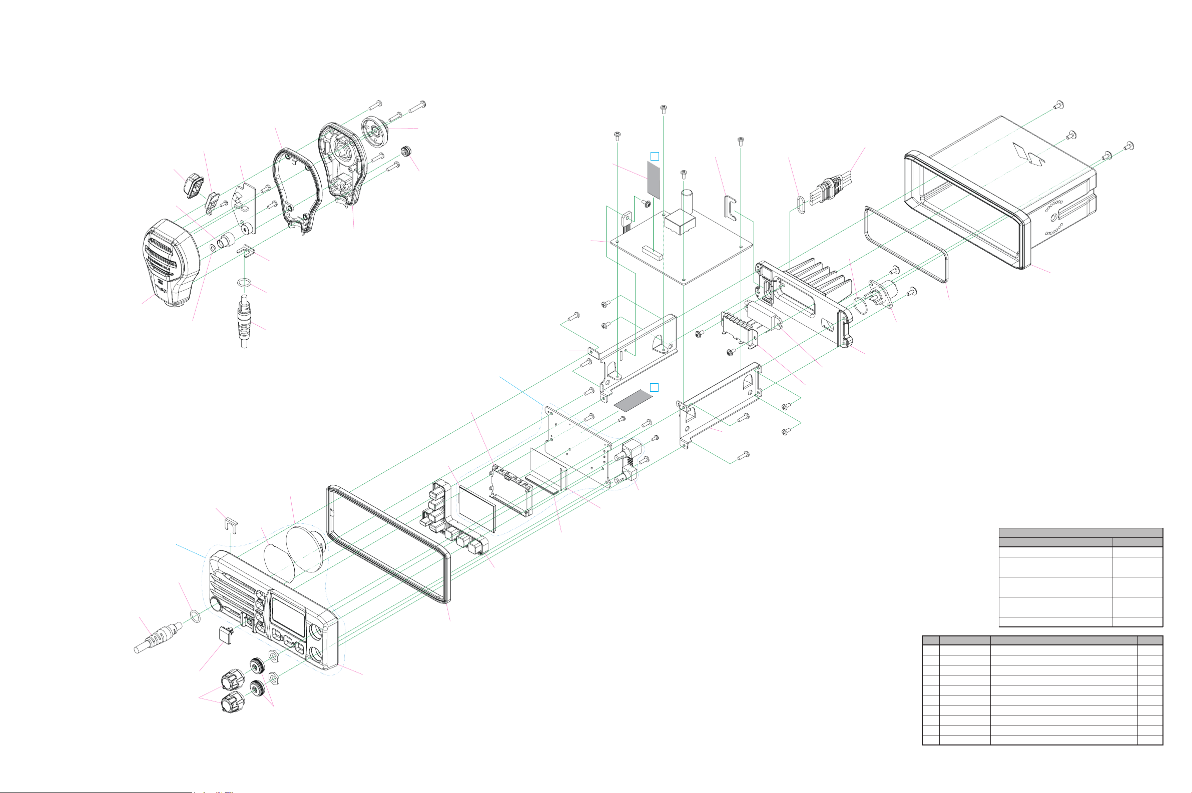
Exploded View & Miscellaneous Parts
CB4557001
MH-76 ASSY (WHITE)
CB4557002
MH-76 ASSY (BLACK)
RA0976400
RUBBER KNOB (PTT)
RA0976300
RUBBER CAP (MIC)
RA0975700 (WHITE)
RA0975800 (BLACK)
FRONT CASE
RA0976600
RUBBER PACKING (MIC)
RA0976700
HOLDER (PTT)
RA0746700
SHEET (M-TEX1131)
MIC UNIT
g
i
i
RA0974600
LOCK PLATE (MIC)
RA0746700
O RING (8x1.5)
T9207455A (WHITE)
T9207454A (BLACK)
WIRE ASSY
k
k
k
k
RA0975900 (WHITE)
RA0976000 (BLACK)
REAR CASE
l
RA0995200 (WHITE)
RA0995300 (BLACK)
HOOK
RA0978700
MIC HOLDER RUBBER
CS1984401 (w/VR UNIT)
CNTL UNIT
RA0975100
LIGHT GUIDE
G6090184
LCD
MAIN UNIT
RA0973700
CHASSIS (L)
T9207450
WIRE ASSY
j
j
j
j
h
h
h
f
h
RA0974500
LOCK PLATE (DC)
A
c
A
h
f
h
h
c
h
RA0974700
RUBBER PACKING (DC)
c
j
RA0973800
CHASSIS (R)
j
j
RA0974400
SHIELD (POWER)
j
T9207449
WIRE ASSY
RA0422900
O RING
e
e
P1091258
CONNECTOR
RA0973400
Q1094559
POWER MODULE (S-AV37A)
HEATSINK
d
d
d
d
RA0973500 (WHITE)
RA0976800 (BLACK)
SLEEVE
RA0974100
RUBBER PACKING (REAR)
RA0974600
LOCK PLATE (MIC)
CP1986101 (WHITE)
CP1986102 (BLACK)
FRONT PANEL ASSY
RA0422900
O RING (M CONECT)
T9207455A (WHITE)
T9207454A (BLACK)
WIRE ASSY
CP9137001
COVER ASSY (DISTRESS)
RA0973100 (WHITE) (2 pcs)
RA0977000 (BLACK) (2 pcs)
VOLUME KNOB
M4090190
SPEAKER
RA0973300
SP NET
Ú1
Ú2
RA0756900 (2 pcs)
PACKING PAD
Ú1: Accessory with VOL Potentiometer
Ú2: Accessory with SQL Potentiometer
RA0972900 (WHITE)
RA0976900 (BLACK)
FRONT PANEL
RA0973000
RUBBER KNOB
RA0974000
RUBBER PACKING (FRONT)
RA0975500
REFLECTOR SHEET
RA0975400
INTER CONNECTOR
VR UNIT
ACCESSORIES
REF.
c
d
e
f
g
h
i
j
k
l
VXSTD P/N
U05206002
U05307020
U20307020
U24105001
U24106001
U24206002
U24208001
U24210002
U24212020
U24316020
DESCRIPTION
DC CABLE
MIC HOLDER (WHITE)
(BLACK)
MOBILE BRACKET (WHITE)
(BLACK)
BRACKET SCREW (WHITE)
(BLACK)
SCREW SET
DESCRIPTION
CAP SCREW TM2.6X6NI
CAP SCREW TM3X7SUS
BINDING HEAD SCREW M3X7SUS
BIND HEAD TAPTITE-B M2X5
BIND HEAD TAPTITE-B M2X6
BIND HEAD TAPTITE-B M2.6X6NI
BIND HEAD TAPTITE-B M2.6X8
BIND HEAD TAPTITE-B M2.6X10NI
BIND HEAD TAPTITE-B 2.6X12SUS
BIND HEAD TAPTITE-B M3X16SUS
VXSTD P/N
T9025406
RA0436000
RA0458800
RA0978300
RA0978400
RA0978500
RA0978600
U9900147
QTY.
3
4
2
2
1
8
2
8
4
1
Non-designated parts are available only as part of a designated assembly.
3
Page 4

Exploded View & Miscellaneous Parts
Note
4
Page 5
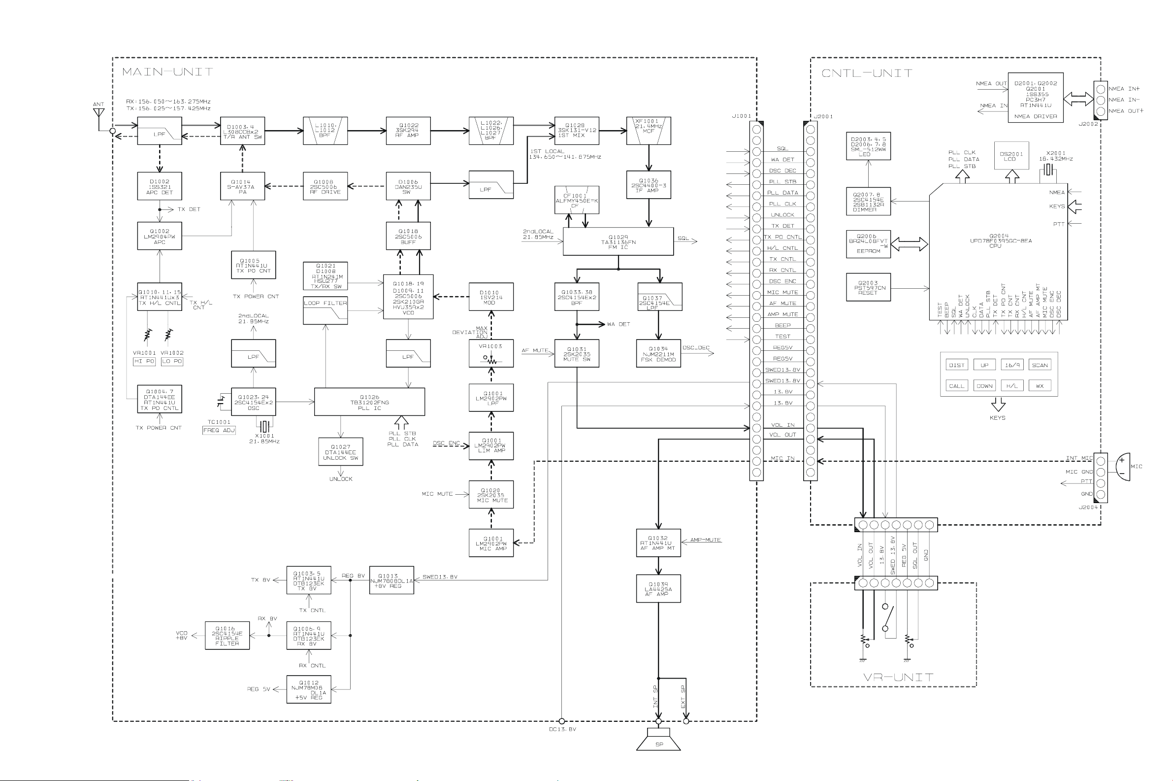
Block Diagram
5
Page 6

Block Diagram
Note
6
Page 7

Circuit Description
Reception and transmission are switched by 8-bit MPU
IC Q2004 (UPD78F0395GC) on the CNTL Unit. The receiver uses double-conversion superheterodyne circuitry, with a 21.4 MHz 1st IF and 450 kHz 2nd IF. The 1st
local is produced by a PLL synthesizer, yielding the 21.4
MHz 1st IF. The 2nd local uses a 21.85 MHz crystal oscillator, yielding the 450 kHz 2nd IF. The 2nd mixer and other
circuits use a custom IC to convert and amplify the 2nd IF
and detect FM to obtain demodulated signals. During
transmit, the PLL synthesizer oscillates at the desired frequency directly, for amplification to obtain RF power output. During transmit, voice modulation is applied to this
synthesizer. Transceiver functions, such as TX/RX control,
PLL synthesizer settings, and channel programming, are
controlled using the MPU.
Receiver
Incoming RF signals from the antenna connector are delivered to the MAIN Unit, and pass through a low-pass
filter (LPF) consisting of coils L1001 & L1002 and capacitors C1003, C1011, & C1024, and antenna switching diode D1004 (L308CCB) for delivery to the receiver front
end.
Signals within the frequency range of the transceiver are
passed through a bandpass filter consisting of coils L1006
& L1008 and capacitors C1027, C1036, & C1059, before RF
amplifier Q1022 (3SK294).
The amplified RF is passed through a bandpass filter consisting of coils L1022, L1026, & L1027 and capacitors
C1145, C1150, C1115, C1159, C1170, C1174, & C1179. The
pure in-band input signal is delivered to the main 1st mixer
Q1028 (3SK131).
Buffered output from the MAIN VCO is amplified by
Q1018 and Q1019 (both 2SC5006) and low-pass filtered
by coils L1009 & L1011 and capacitors C1064, C1071, &
C1076, to provide a pure 1st local signal between 134.625
and 136.025 MHz for delivery to the main 1st mixer.
The 21.4 MHz 1st mixer product is passed through the
monolithic crystal filter XF1001 (±6.5 kHz BW), and is
amplified by Q1036 (2SC4400).
After that, it delivered to the input of the FM IF subsystem
IC Q1029 (TA31136FNG). This IC contains the 2nd mixer, 2nd local oscillator, limiter amplifier, FM detector, noise
amplifier, and squelch gates.
The 2nd local in the FM IF subsystem IC Q1029
(TA31136FNG) is produced from crystal X1001 (21.850
MHz), and the 1st IF is converted to 450 kHz by the 2nd
mixer and stripped of unwanted components by ceramic
filter CF1001.
After passing through a limiter amplifier, the signal is
demodulated by the FM detector. Demodulated audio
from the FM IF subsystem IC Q1029 (TA31136FNG) is
amplified by Q1038 and Q1033 (both 2SC4154). The amplified signal is passed through the AF mute switch Q1031
(2SK2035) and the front panels volume control. The adjusted audio signal is delivered to the AF power amplifier Q1039 (LA4425A).
The amplified audio signal is delivered to the 8 Ohms internal loudspeaker and external Speaker terminal in the
accessory cable.
PLL Synthesizer
The 1st Local signal maintains stability from the PLL synthesizer by using a 21.850 MHz reference signal from crystal X1001. PLL synthesizer IC Q1026 (TB31202FNG) con-
sists of a prescaler, reference counter, swallow counter,
programmable counter, a serial data input port to set these
counters based on the external data, a phase comparator,
and a charge pump.
The PLL synthesizer IC divides the 21.850 MHz reference
signal by 1748 using the reference counter (12.5 kHz comparison frequency).
The VCO output is divided by the prescaler, swallow
counter and programmable counter. These two signals are
compared by the phase comparator, and applied to the
charge pump.
A voltage proportional to their phase difference is delivered to the low-pass filter circuit, then fed back to the VCO
as a voltage with phase error, controlling and stabilizing
the oscillating frequency. This synthesizer also operates
as a modulator during transmit.
The VCO consists of Q1019 (2SK210GR) and varactor di-
odes D1009 and D1011 (both HVU359), which oscillates
at 21.4 MHz below from the receiving frequency while
receiving, and oscillates at the fundamental transmit frequency during a transmit with direct frequency-modulation using varactor diode D1010 (1SV214). The VCO output passes through buffer amplifier Q1018 and Q1017
(both 2SC5006) to obtain stable output, then applied to
the 1st mixer of while receiving, and to the driver amplifier Q1008 (2SC5006) during a transmit.
The DC supply for the VCO is regulated by Q1016
(2SC4154).
7
Page 8

Circuit Description
Transmitter
The voice from the microphone is passed through the
CNTL Unit to the microphone amplifier Q1001
(LM2902PW) on the MAIN Unit, a pre-emphasis network,
limiter (IDC: instantaneous deviation control), and lowpass filter network, the audio is adjusted for optimum deviation level.
The voice or DSC (Digital Selective Calling) encoded signal from the low-pass filter network Q1001 (LM2902PW)
is applied to the VCO Q1019 (2SK210GR) which oscil-
lates at the fundamental transmit frequency with direct
frequency-modulation using varactor diode D1010
(1SV214). The modulated signal is amplified by the buffer amplifier Q1018 and Q1017 (both 2SC5006), then
passed through the diode switch D1006 (DAN235U) to
drive amplifiers Q1008 (2SC5006) and RF power amplifier module Q1014 (S-AV37A).
The RF energy then passes through antenna switch D1003
(L308CCB) and low-pass filter (LPF) consisting of coils
L1001 & L1002 and capacitors C1003, C1011, & C1024, and
finally to the antenna connector.
RF output power from the RF power amplifier module
Q1014 (S-AV37A) is sampled by C1014 and C1021 and is
rectified by D1002 (1SS321). The resulting DC is fed
through Automatic Power Controller Q1007 (RT1N441U)
to RF power amplifier module Q1014 (S-AV37A), thus pro-
viding positive control of the power output.
Generation of spurious products by the transmitter is minimized by the fundamental carrier frequency being equal
to the final transmitting frequency, modulated directly in
the transmit VCO. Additional harmonic suppression is
provided by a low-pass filter consisting of coils and capacitors, resulting in more than 80 dB of harmonic suppression prior to delivery of the RF energy to the antenna.
DSC Encoder/ Decoder
Encoder
The DSC (Digital Selective Calling) encode signal which
D/A converted in the 8-bit MPU Q2004 (UPD78F0395GC)
on the CNTL Unit is fed through the low-pass filter Q1001
(LM2902PWR) on the MAIN Unit to the VCO Q1019
(2SK210GR).
Decoder
A portion of the demodulated signal from the FM IF subsystem IC Q1029 (TA31136FNG) is passes through the
low-pass filter Q1037 (2SC4154) to the DSC Decoder IC
Q1034 (NJM2211M). The decoded DCS signal delivered
to the 8-bit MPU IC Q2004 (UPD78F0395GC) on the
CNTL Unit.
1050 Hz Weather Alert Decoder
The 1050 Hz Weather Alert signal from the buffer amplifier Q1033 (2SC4154) is applied to 8-bit MPU IC Q2004
(UPD78F0395GC) on the CNTL Unit.
MPU
Operation is controlled by 8-bit MPU IC Q2004
(UPD78F0395GC) on the CNTL Unit. This MPU uses a
18.432 MHz crystal X2001 for the system clock. IC Q2003
(PST597CN) resets the MPU when the power is on.
EEPROM
The EEPROM Q2006 (BR24L08FVT) on the CNTL Unit
retains TX and RX data for all memory channels, prescaler dividing, IF frequency, local oscillator injection side,
and reference oscillator data.
8
Page 9

Alignment
The GX1000S has been carefully aligned at the factory
for the specified performance across the marine band.
Realignment should therefore not be necessary except in
the event of a component failure. All component replacement and service should be performed only by an authorized Standard Horizon representative, or the warranty
policy may be voided.
The following procedures cover the sometimes critical and
tedious adjustments that are not normally required once
the transceiver has left the factory. However, if damage
occurs and some parts are replaced, realignment may be
required. If a sudden problem occurs during normal operation, it is likely due to component failure; realignment
should not be done until after the faulty component has
been replaced.
We recommend that servicing be performed only by authorized Standard Horizon service technicians who are
experienced with the circuitry and fully equipped for repair and alignment. Therefore, if a fault is suspected, contact the dealer from whom the transceiver was purchased
for instructions regarding repair. Authorized Standard
Horizon service technicians realign all circuits and make
complete performance checks to ensure compliance with
factory specifications after replacing any faulty components.
Those who do undertake any of the following alignments
are cautioned to proceed at their own risk. Problems
caused by unauthorized attempts at realignment are not
covered by the warranty policy. Also, Standard Horizon,
a division of Vertex Standard must reserve the right to
change circuits and alignment procedures in the interest
of improved performance, without notifying owners.
Under no circumstances should any alignment be attempted unless the normal function and operation of the transceiver are clearly understood, the cause of the malfunction has been clearly pinpointed and any faulty components replaced, and the need for realignment determined
to be absolutely necessary.
The following test equipment (and thorough familiarity
with its correct use) is necessary for complete realignment.
Correction of problems caused by misalignment resulting from use of improper test equipment is not covered
under the warranty policy. While most steps do not require all of the equipment listed, the interactions of some
adjustments may require that more complex adjustments
be performed afterwards. Do not attempt to perform only
a single step unless it is clearly isolated electrically from
all other steps. Have all test equipment ready before beginning, and follow all of the steps in a section in the order presented.
Required Test Equipment
RF Signal Generator with calibrated output level at
200 MHz
Deviation Meter (linear detector)
AF Millivoltmeter
SINAD Meter
Inline Wattmeter with 5% accuracy at 200 MHz
Regulated DC Power Supply: 13.8 VDC, 10A
50-ohm Non-reactive Dummy Load: 30W at 200 MHz
Frequency Counter: >0.1 ppm accuracy at 200 MHz
AF Signal Generator
DC Voltmeter: high impedance
VHF Sampling Coupler
AF Dummy Load: 4 Ohms, 10 W
Oscilloscope
Spectrum Analyzer
CP180 GPS/Chart Plotter
GX5500S Marine Transceiver
Alignment Preparation & Precautions
A dummy load and inline wattmeter must be connected
to the main antenna jack in all procedures that call for
transmission. Correct alignment is not possible with an
antenna.
After completing one step, read the following step to determine whether the same test equipment will be required.
If not, remove the test equipment (except dummy load
and wattmeter, if connected) before proceeding.
Correct alignment requires that the ambient temperature
be the same as that of the transceiver and test equipment,
and that this temperature be held constant between 68 °F
and 86 °F (20 °C and 30 °C). When the transceiver is
brought into the shop from hot or cold air it should be
allowed some time for thermal equalization with the environment before alignment. If possible, alignments
should be made with oscillator shields and circuit boards
firmly affixed in place. Also, the test equipment must be
thoroughly warmed up before beginning.
Note: Signal levels in dB referred to in this procedure are
based on 0 dBμ = 0.5 μV (closed circuit).
9
Page 10
Alignment
Main Reference Frequency Adjustment
Setup the test equipment as shown below.
Sampling
50-ohm
Dummy Load
Frequency
Counter
Set the channel to CH16.
Use the [H/L] key to set the transceiver to “LOW”
power.
With the PTT switch pressed, adjust TC1001 so that the
Frequency Counter reading is 156.800 MHz ±100 Hz.
VR1001
Coupler
ANT
GX1000S
Transmit Power Adjustment
Setup the test equipment as shown below.
50-ohm
Dummy Load
Set the channel to CH16.
Use the [H/L] key to set the transceiver to “HI” power.
With the PTT switch pressed, adjust VR1001 so that
RF output power is 24 W ±0.3 W.
Release the PTT switch, then set the transceiver to
“LOW” power by the [H/L] key.
With the PTT switch pressed, adjust VR1002 so that
RF output power is 0.8 W ±0.1 W.
Release the PTT switch.
Inline
Wattmeter
ANT
GX1000S
L1022
VR1002
L1027
VR1003
TC1001
JP1001
L1022
L1012
L1010
TP1008
10
MAIN UNIT ALIGNMENT POINT
Page 11

Alignment
A
TX Deviation Adjustment
Setup the test equipment as shown below.
Sampling
50-ohm
Dummy Load
Deviation
Meter
Set the AF Signal Generator output to 200 mVrms at 1
kHz.
Set the channel to CH16.
With the PTT switch pressed, adjust VR1003 so that
the maximum deviation is 4.2 kHz ±0.1 kHz.
Release the PTT switch.
Coupler
GX1000S
ANT Pin 4
J2004
AF Signal
Generator
Receiver Front-end Adjustment
Setup the test equipment as shown below.
Tracking
Generator
GX1000S
ANT TP1008
Set the spectrum analyzer as shown below:
CENTER: 159.000 MHz
SPAN: 20.000 MHz
RBW, VBW: 30 kHz
SWP: 200 ms
Adjust L1010, L1012, L1022, L1026, and L1027 until
the wave form shown in below is obtained.
TTEN 10dB
RL 10.0dBm 10dB/
Spectrum
Analizer
GX1000S-FRONT-END
CENTER 159.00 0 MHz
RBW 30 kHz VBW 30 kHz
SPAN 20.00 MHz
SWP 200 ms
Pin 4
of J2004
CNTL UNIT ALIGNMENT POINT
11
Page 12

Alignment
Software Alignment/Confirmation Mode
Overview of Software Alignment Mode
The “Software Alignment Mode” has been build in the
microprocessor in order to adjust and confirm the performance of transceiver.
The purpose is to adjust transceiver simply and to confirm the performance of transceiver smoothly.
Starting Software Alignment Mode
Set the channel to CH16, then turn the VOL knob
counter clockwise to turn off the radio.
Short the TEST points (JP1001).
Setup the test equipment as shown below.
RF Signal
Generator
Turn the VOL knob clockwise to turn on the radio
while press and holding the
[
CALL(SET)MENU
TRESS] keys. The LCD will be as
shown in the illustration at the right.
Press the [SCAN(MEM)] key to re-
call the Alignment Item “THxxx”.
Set the RF Signal Generator output
to 156.800 MHz, at a level of –9dBμ,
±3.0 kHz deviation with a 1 kHz audio tone.
Press the [WX] key.
Press the [CALL(SET)MENU] key to save the new set-
ting.
Press the [SCAN(MEM)] key to re-
call the Alignment Item “TIxxx”.
Set the RF Signal Generator output
to 156.800 MHz, at a level of +3dBμ,
±3.0 kHz deviation with a 1 kHz audio tone.
Press the [WX] key.
Press the [CALL(SET)MENU] key to save the new set-
ting.
] and [
DIS-
ANT
GX1000S
Press the [SCAN(MEM)] key to re-
call the Alignment Item “SBxxx”.
Set the RF Signal Generator output
to 156.525 MHz, at a level of –4dBμ,
±3.0 kHz deviation with a 1 kHz audio tone.
Press the [WX] key.
Press the [CALL(SET)MENU] key to save the new set-
ting.
Press the [SCAN] key to recall the
Alignment Item “VTxxx”.
Press the [WX] key.
Press the [CALL(SET)MENU] key to
save the new setting.
This completes the Software Alignment Mode. To save
all settings and exit, press and hold the [DISTRESS] key
for one second. Turn the transceiver’s power off, then disconnect the Jumper from the TEST points (JP1001).
12
Page 13

MAIN Unit
Circuit Diagram
TX HI: 4.0 V
TX LOW: 0.6 V
TX: 8.0 V
TX: 1.4 V
TX: 1.8 V
TX: 7.3 V
TX: 2.2 V
13.8 V
RX: 0 V
TX: 4.4 V
TX HI: 3.0 V
TX LOW: 1.5 V
RX: 4.4 V
TX: 0 V
6.9 V
3.3 V
7.2 V
3.9 V
RX: 2.9 V
RX: 1.2 V
5.7 V 6.7 V
0.8 V
0.1 V
RX: 8.0 V
TX: 0 V
RX: 6.0 V
RX: 7.4 V
TX: 3.7 V
RX: 4.0 V
TX: 0 V
RX: 5.6 V
RX: 7.8 V
RX: 0.2 V
RX: 1.1 V
RX: 7.8 V
RX: 0.4 V
RF –9 dBμV(emf): 3.8 V
RF +3 dBμV(emf): 1.6 V
RX: 5.3 V
TX HI: 0 V
TX LOW: 5.0 V
RX: 0 V
TX: 8.0 V
RX: 0 V
TX: 5.0 V
13.8 V
RX: 5.0 V
TX: 0 V
RX: 8.0 V
8.0 V 5.0 V
TX: 0 V
RX: 5.0 V
TX: 0 V
POWER "ON": 13.8 V
8.0 V
TX HI: 3.8 V
TX LOW: 0.7 V
MIC MUTE "OFF": 5.0 V
MIC MUTE "ON": 0 V
2.4 V
2.2 V
4.9 V
1.8 V
1.8 V
4.3 V
1.2 V
4.6 V
4.8 V
5.0 V
PLL "LOCK": 0 V
PLL "UNLOCK": 5.0 V
AF MUTE "OFF": 5.0 V
AF MUTE "ON": 0 V
RX: 5.1 V
RX: 1.5 V
RX: 2.3 V
RX: 3.5 V
RX: 2.1 V
RX: 0.7 V
RX: 2.9 V
RX: 2.2 V
RX: 1.3 V
13.8 V
2.5 V
5.0 V
AMP MUTE "OFF": 0 V
AMP MUTE "ON": 5.0 V
13
Page 14

MAIN Unit
Note
14
Page 15

MAIN Unit
Parts Layout (Side A)
BA DC E
S-AV37X
(Q1014)
TA31136FNG
(Q1029)
TB31202FNG
(Q1026)
LA4425A
(Q1039)
2SK210-GR (YG)
(Q1019)
NJM2211M
(Q1034)
LM2902PWR
(Q1001)
2SC4154 (LE)
(Q1016, 1023,
1024, 1033, 1035,
1037, 1038)
2SC5006 (24)
(Q1017, 1018)
2SK2035 (KP)
(Q1031)
1
2
DTA144EE (16)
(Q1004, 1027)
RT1N441U (N3)
(Q1003, 1006, 1010,
1011, 1015, 1041)
TC4S66F (C9)
(Q1040)
1SS321 (F9)
(D1002)
DTB123EK (F52)
(Q1005, 1009)
RT1N241M (N2)
(Q1021)
MC2850 (A7)
(D1013, 1014)
3
4
5
15
Page 16

MAIN Unit
Parts Layout (Side B)
ba dc e
NJM7808DL1A
(Q1013)
NJM78M05DL1A
(Q1012)
LM2904PWR
(Q1002)
1
3SK131 (V12)
(Q1028)
3SK294 (UV)
(Q1022)
2
2SK2035 (KP)
(Q1032)
RT1N441U (N3)
3
(Q1007)
2SC4400 (RT4)
(Q1036)
2SC5006 (24)
(Q1008)
4
5
16
DAN235U (M)
(D1006)
Page 17

MAIN Unit
Parts List
REF DESCRIPTION VALUE V/W TOL. MFR'S DESIG VXSTD P/N VERS.
P.C.B. with Components CS1983701
Printed Circuit Board AM030N000 FR017520C 1C 1001 CHIP CAP. 0.001uF 50V B GRM188B11H102KA01D K22174821 1- A B5
C 1002 CHIP CAP. 0.001uF 50V B GRM188B11H102KA01D K22174821 1- A B4
C 1003 CHIP CAP. 15pF 500V CH 1206N150J501LT K22278211 1- B a1
C 1004 CHIP CAP. 0.001uF 50V B GRM188B11H102KA01D K22174821 1- B d1
C 1005 CHIP CAP. 0.01uF 50V B GRM188B11H103KA01D K22174823 1- A B4
C 1006 CHIP CAP. 4pF 50V CH GRM1882C1H4R0CZ01D K22174205 1- A D1
C 1007 CHIP CAP. 0.1uF 16V B GRM188B11C104KA01D K22124805 1- B b1
C 1010 CHIP CAP. 10pF 50V CH GRM1882C1H100JA01D K22174211 1- B d1
C 1011 CHIP CAP. 27pF 500V CH 1206N270J501LT K22278214 1- B b1
C 1012 CHIP CAP. 6pF 50V CH GRM1882C1H6R0DZ01D K22174207 1- B d1
C 1013 CHIP CAP. 0.1uF 16V B GRM188B11C104KA01D K22124805 1- B b1
C 1014 CHIP CAP. 1pF 50V CK GRM1884C1H1R0CZ01D K22174202 1- A D1
C 1015 AL.ELECTRO.CAP. 1000uF 25V SL025M102G20PKKKS00R K40149072 1- A A1
C 1016 CHIP CAP. 0.1uF 16V B GRM188B11C104KA01D K22124805 1- B d1
C 1019 CHIP CAP. 0.001uF 50V B GRM188B11H102KA01D K22174821 1- A B5
C 1020 CHIP CAP. 0.001uF 50V B GRM188B11H102KA01D K22174821 1- A C1
C 1021 CHIP CAP. 1pF 50V CK GRM1884C1H1R0CZ01D K22174202 1- A D1
C 1022 CHIP CAP. 0.001uF 50V B GRM188B11H102KA01D K22174821 1- B b1
C 1023 CHIP CAP. 10pF 50V CH GRM1882C1H100JA01D K22174211 1- A B5
C 1024 CHIP CAP. 18pF 500V CH 1206N180J501LT K22278212 1- B b1
C 1025 CHIP CAP. 0.001uF 50V B GRM188B11H102KA01D K22174821 1- B d1
C 1027 CHIP CAP. 47pF 500V CH 1206N470J501LT K22278217 1- B b1
C 1028 CHIP CAP. 3pF 50V CJ GRM1883C1H3R0CZ01D K22174204 1- A D1
C 1029 CHIP CAP. 0.001uF 50V B GRM188B11H102KA01D K22174821 1- B d1
C 1030 CHIP CAP. 0.001uF 50V B GRM188B11H102KA01D K22174821 1- A D1
C 1031 CHIP CAP. 22pF 500V CH 1206N220J501LT K22278213 1- B b1
C 1032 CHIP CAP. 0.01uF 50V B GRM188B11H103KA01D K22174823 1- A B4
C 1033 CHIP CAP. 6pF 50V CH GRM1882C1H6R0DZ01D K22174207 1- B d1
C 1034 CHIP CAP. 10pF 50V CH GRM1882C1H100JA01D K22174211 1- B d5
C 1035 CHIP CAP. 0.001uF 50V B GRM188B11H102KA01D K22174821 1- A B4
C 1036 CHIP CAP. 15pF 50V CH GRM1882C1H150JA01D K22174215 1- B a1
C 1037 CHIP CAP. 0.001uF 50V B GRM188B11H102KA01D K22174821 1- B d1
C 1038 CHIP CAP. 22pF 500V CH 1206N220J501LT K22278213 1- B b1
C 1039 CHIP CAP. 0.1uF 25V F GRM188F11E104ZA01D K22145001 1- B d5
C 1040 CHIP TA.CAP. 4.7uF 10V F931A475MAA K78100077 1- B d1
C 1041 CHIP CAP. 0.001uF 50V B GRM188B11H102KA01D K22174821 1- B c1
C 1042 CHIP CAP. 10pF 50V CH GRM1882C1H100JA01D K22174211 1- B d5
C 1043 CHIP CAP. 0.001uF 50V B GRM188B11H102KA01D K22174821 1- B d1
C 1044 CHIP CAP. 0.001uF 50V B GRM188B11H102KA01D K22174821 1- B d5
C 1045 CHIP CAP. 0.22uF 10V B GRM188B11A224KA01D K22104801 1- B c1
C 1047 AL.ELECTRO.CAP. 10uF 25V SS025M100C07PKKKS00R K40149075 1- A C1
C 1048 AL.ELECTRO.CAP. 10uF 25V SS025M100C07PKKKS00R K40149075 1- A B5
C 1049 CHIP CAP. 10pF 50V CH GRM1882C1H100JA01D K22174211 1- B c1
C 1050 AL.ELECTRO.CAP. 47uF 25V SL025M470D11PKKKS00R K40149074 1- A B5
C 1051 CHIP CAP. 0.001uF 50V B GRM188B11H102KA01D K22174821 1- B c1
C 1053 CHIP CAP. 0.001uF 50V B GRM188B11H102KA01D K22174821 1- B d1
C 1054 CHIP CAP. 0.001uF 50V B GRM188B11H102KA01D K22174821 1- B d5
C 1055 CHIP CAP. 0.001uF 50V B GRM188B11H102KA01D K22174821 1- B d1
C 1056 CHIP CAP. 0.22uF 10V B GRM188B11A224KA01D K22104801 1- B d1
C 1057 CHIP CAP. 0.1uF 16V B GRM188B11C104KA01D K22124805 1- B d1
C 1058 CHIP CAP. 0.001uF 50V B GRM188B11H102KA01D K22174821 1- B d2
C 1059 CHIP CAP. 47pF 50V CH GRM1882C1H470JA01D K22174227 1- B a2
C 1060 CHIP CAP. 0.001uF 50V B GRM188B11H102KA01D K22174821 1- B c2
C 1061 CHIP CAP. 9pF 50V CH GRM1882C1H9R0DZ01D K22174210 1- B a2
C 1062 CHIP CAP. 0.001uF 50V B GRM188B11H102KA01D K22174821 1- A B1
C 1063 CHIP CAP. 0.001uF 50V B GRM188B11H102KA01D K22174821 1- B e5
C 1064 CHIP CAP. 12pF 50V CH GRM1882C1H120JA01D K22174213 1- B c2
C 1065 CHIP CAP. 0.001uF 50V B GRM188B11H102KA01D K22174821 1- B c1
C 1066 CHIP CAP. 0.01uF 50V B GRM188B11H103KA01D K22174823 1- B d5
C 1067 CHIP CAP. 2pF 50V CK GRM1884C1H2R0CZ01D K22174203 1- B a2
C 1068 CHIP TA.CAP. 10uF 10V F931A106MAA K78100078 1- A B1
C 1069 CHIP CAP. 0.01uF 50V B GRM188B11H103KA01D K22174823 1- B e5
C 1070 CHIP CAP. 0.001uF 50V B GRM188B11H102KA01D K22174821 1- B d5
C 1071 CHIP CAP. 39pF 50V CH GRM1882C1H390JA01D K22174225 1- B c2
C 1072 CHIP CAP. 0.1uF 16V B GRM188B11C104KA01D K22124805 1- A B1
C 1073 CHIP TA.CAP. 10uF 10V F931A106MAA K78100078 1- B e4
C 1074 CHIP CAP. 0.75pF 50V CK GRM1884C1HR75CZ01D K22174260 1- B a2
C 1075 CHIP CAP. 10pF 50V CH GRM1882C1H100JA01D K22174211 1- B e5
C 1076 CHIP CAP. 12pF 50V CH GRM1882C1H120JA01D K22174213 1- B c2
C 1077 CHIP CAP. 6pF 50V CH GRM1882C1H6R0DZ01D K22174207 1- B a2
C 1078 CHIP CAP. 0.001uF 50V B GRM188B11H102KA01D K22174821 1- B c1
LOT
SIDE
LAY ADR
17
Page 18

MAIN Unit
Parts List
REF DESCRIPTION VALUE V/W TOL. MFR'S DESIG VXSTD P/N VERS.
C 1079 CHIP CAP. 7pF 50V CH GRM1882C1H7R0DZ01D K22174208 1- B c2
C 1080 CHIP CAP. 0.001uF 50V B GRM188B11H102KA01D K22174821 1- A A2
C 1081 CHIP CAP. 0.001uF 50V B GRM188B11H102KA01D K22174821 1- A B1
C 1082 CHIP CAP. 0.01uF 50V B GRM188B11H103KA01D K22174823 1- B c1
C 1083 CHIP CAP. 10pF 50V CH GRM1882C1H100JA01D K22174211 1- B a2
C 1084 CHIP TA.CAP. 10uF 10V F931A106MAA K78100078 1- A A2
C 1086 CHIP TA.CAP. 10uF 10V F931A106MAA K78100078 1- A A2
C 1087 CHIP CAP. 1pF 50V CK GRM1884C1H1R0CZ01D K22174202 1- A B2
C 1089 CHIP TA.CAP. 10uF 10V F931A106MAA K78100078 1- B b5
C 1090 CHIP CAP. 0.001uF 50V B GRM188B11H102KA01D K22174821 1- A A2
C 1091 CHIP CAP. 0.001uF 50V B GRM188B11H102KA01D K22174821 1- B b2
C 1092 CHIP CAP. 10pF 50V CH GRM1882C1H100JA01D K22174211 1- B b2
C 1093 CHIP CAP. 0.0056uF 50V B GRM188B11H562KA01D K22174818 1- A D4
C 1094 CHIP CAP. 15pF 50V CH GRM1882C1H150JA01D K22174215 1- A D5
C 1095 CHIP CAP. 0.001uF 50V B GRM188B11H102KA01D K22174821 1- B b2
C 1097 CHIP CAP. 0.001uF 50V B GRM188B11H102KA01D K22174821 1- B b2
C 1098 CHIP CAP. 0.001uF 50V B GRM188B11H102KA01D K22174821 1- A B2
C 1100 CHIP CAP. 1uF 6.3V B GRM188B10J105KA01D K22084801 1- A D4
C 1102 CHIP CAP. 15pF 50V CH GRM1882C1H150JA01D K22174215 1- A D4
C 1103 CHIP CAP. 0.001uF 50V B GRM188B11H102KA01D K22174821 1- A B2
C 1104 CHIP CAP. 1pF 50V CK GRM1884C1H1R0CZ01D K22174202 1- A B2
C 1105 CHIP CAP. 5pF 50V CH GRM1882C1H5R0CZ01D K22174206 1- A D2
C 1106 CHIP CAP. 0.1uF 16V B GRM188B11C104KA01D K22124805 1- A B2
C 1107 CHIP CAP. 0.1uF 16V B GRM188B11C104KA01D K22124805 1- A D4
C 1108 CHIP CAP. 0.01uF 50V B GRM188B11H103KA01D K22174823 1- A D4
C 1109 CHIP CAP. 6pF 50V CH GRM1882C1H6R0DZ01D K22174207 1- B d3
C 1111 CHIP CAP. 0.001uF 50V B GRM188B11H102KA01D K22174821 1- A D2
C 1112 CHIP CAP. 1uF 6.3V B GRM188B10J105KA01D K22084801 1- A D4
C 1113 CHIP CAP. 56pF 50V CH GRM1882C1H560JA01D K22174229 1- B d3
C 1114 CHIP CAP. 5pF 50V CH GRM1882C1H5R0CZ01D K22174206 1- A B2
C 1115 CHIP CAP. 6pF 50V CH GRM1882C1H6R0DZ01D K22174207 1- A B2
C 1117 CHIP CAP. 15pF 50V CH GRM1882C1H150JA01D K22174215 1- A D4
C 1118 CHIP CAP. 0.001uF 50V B GRM188B11H102KA01D K22174821 1- B b2
C 1119 CHIP CAP. 33pF 50V CH GRM1882C1H330JA01D K22174223 1- B d3
C 1120 CHIP CAP. 0.001uF 50V B GRM188B11H102KA01D K22174821 1- A B2
C 1121 CHIP CAP. 47pF 50V CH GRM1882C1H470JA01D K22174227 1- A A3
C 1122 CHIP CAP. 6pF 50V CH GRM1882C1H6R0DZ01D K22174207 1- A B2
C 1123 CHIP CAP. 10pF 50V CH GRM1882C1H100JA01D K22174211 1- B d3
C 1125 CHIP CAP. 5pF 50V CH GRM1882C1H5R0CZ01D K22174206 1- B d3
C 1127 CHIP CAP. 0.001uF 50V B GRM188B11H102KA01D K22174821 1- B b2
C 1128 CHIP CAP. 0.001uF 50V B GRM188B11H102KA01D K22174821 1- A B2
C 1129 CHIP TA.CAP. 10uF 10V F931A106MAA K78100078 1- A A3
C 1130 CHIP CAP. 27pF 50V CH GRM1882C1H270JA01D K22174221 1- A A3
C 1131 CHIP CAP. 7pF 50V CH GRM1882C1H7R0DZ01D K22174208 1- A A3
C 1132 CHIP CAP. 1uF 6.3V B GRM188B10J105KA01D K22084801 1- A D4
C 1133 CHIP TA.CAP. 4.7uF 10V F931A475MAA K78100077 1- B b4
C 1134 CHIP CAP. 10pF 50V CH GRM1882C1H100JA01D K22174211 1- B b2
C 1135 CHIP CAP. 0.001uF 50V B GRM188B11H102KA01D K22174821 1- B b2
C 1137 CHIP CAP. 0.01uF 50V B GRM188B11H103KA01D K22174823 1- A A3
C 1138 CHIP CAP. 1uF 6.3V B GRM188B10J105KA01D K22084801 1- B b4
C 1140 CHIP CAP. 0.0068uF 50V B GRM188B11H682KA01D K22174834 1- A D4
C 1141 CHIP CAP. 1pF 50V CK GRM1884C1H1R0CZ01D K22174202 1- A B2
C 1144 CHIP CAP. 0.001uF 50V B GRM188B11H102KA01D K22174821 1- B b4
C 1145 CHIP CAP. 4pF 50V CH GRM1882C1H4R0CZ01D K22174205 1- B b2
C 1146 CHIP CAP. 0.01uF 50V B GRM188B11H103KA01D K22174823 1- A B3
C 1148 CHIP CAP. 15pF 50V CH GRM1882C1H150JA01D K22174215 1- A A3
C 1150 CHIP CAP. 4pF 50V CH GRM1882C1H4R0CZ01D K22174205 1- B b2
C 1152 CHIP CAP. 15pF 50V CH GRM1882C1H150JA01D K22174215 1- A B2
C 1153 CHIP CAP. 330pF 50V B GRM188B11H331KD01D K22174820 1- A D4
C 1155 CHIP CAP. 0.5pF 50V CK GRM1884C1HR50CZ01D K22174201 1- B b2
C 1159 CHIP CAP. 5pF 50V CH GRM1882C1H5R0CZ01D K22174206 1- B c2
C 1160 CHIP CAP. 82pF 50V CH GRM1882C1H820JA01D K22174233 1- A B3
C 1161 CHIP CAP. 82pF 50V CH GRM1882C1H820JA01D K22174233 1- A B3
C 1162 CHIP CAP. 10pF 50V CH GRM1882C1H100JA01D K22174211 1- A B3
C 1163 CHIP CAP. 100pF 50V CH GRM1882C1H101JA01D K22174235 1- A B3
C 1165 CHIP CAP. 10pF 50V CH GRM1882C1H100JA01D K22174211 1- A B3
C 1166 CHIP CAP. 0.0056uF 50V B GRM188B11H562KA01D K22174818 1- A D4
C 1168 CHIP CAP. 0.001uF 50V B GRM188B11H102KA01D K22174821 1- B b4
C 1169 CHIP CAP. 0.001uF 50V B GRM188B11H102KA01D K22174821 1- A D2
C 1170 CHIP CAP. 0.5pF 50V CK GRM1884C1HR50CZ01D K22174201 1- B c2
C 1171 CHIP CAP. 0.001uF 50V B GRM188B11H102KA01D K22174821 1- A D2
C 1172 CHIP TA.CAP. 10uF 10V F931A106MAA K78100078 1- B b4
C 1174 CHIP CAP. 3pF 50V CJ GRM1883C1H3R0CZ01D K22174204 1- B c2
LOT
SIDE
LAY ADR
18
Page 19

MAIN Unit
Parts List
REF DESCRIPTION VALUE V/W TOL. MFR'S DESIG VXSTD P/N VERS.
C 1175 CHIP TA.CAP. 0.33uF 35V F931V334MAA K78160054 1- B d3
C 1179 CHIP CAP. 3pF 50V CJ GRM1883C1H3R0CZ01D K22174204 1- B c2
C 1181 CHIP CAP. 1uF 6.3V B GRM188B10J105KA01D K22084801 1- B b4
C 1183 CHIP CAP. 1uF 6.3V B GRM188B10J105KA01D K22084801 1- A A3
C 1189 CHIP TA.CAP. 2.2uF 6.3V F930J225MAA K78080093 1- B d3
C 1194 CHIP CAP. 0.001uF 50V B GRM188B11H102KA01D K22174821 1- A B3
C 1196 CHIP CAP. 0.01uF 50V B GRM188B11H103KA01D K22174823 1- A B3
C 1197 CHIP CAP. 22pF 50V CH GRM1882C1H220JA01D K22174219 1- B c2
C 1198 CHIP TA.CAP. 10uF 10V F931A106MAA K78100078 1- A B3
C 1199 CHIP TA.CAP. 0.47uF 35V F931V474MAA K78160055 1- B d3
C 1200 CHIP CAP. 0.001uF 50V B GRM188B11H102KA01D K22174821 1- B c2
C 1201 CHIP CAP. 0.001uF 50V B GRM188B11H102KA01D K22174821 1- B c2
C 1202 CHIP CAP. 0.1uF 16V B GRM188B11C104KA01D K22124805 1- B b4
C 1203 CHIP CAP. 0.01uF 50V B GRM188B11H103KA01D K22174823 1- A B3
C 1204 CHIP CAP. 0.001uF 50V B GRM188B11H102KA01D K22174821 1- B b3
C 1205 CHIP CAP. 0.01uF 50V B GRM188B11H103KA01D K22174823 1- A B3
C 1206 AL.ELECTRO.CAP. 10uF 25V SS025M100C07PKKKS00R K40149075 1- A C3
C 1207 CHIP CAP. 0.001uF 50V B GRM188B11H102KA01D K22174821 1- B c2
C 1210 CHIP CAP. 0.01uF 50V B GRM188B11H103KA01D K22174823 1- B c2
C 1212 CHIP CAP. 33pF 50V CH GRM1882C1H330JA01D K22174223 1- B c3
C 1213 CHIP CAP. 0.001uF 50V B GRM188B11H102KA01D K22174821 1- B c3
C 1214 CHIP CAP. 0.1uF 16V B GRM188B11C104KA01D K22124805 1- A C3
C 1216 CHIP CAP. 0.001uF 50V B GRM188B11H102KA01D K22174821 1- A C3
C 1218 CHIP CAP. 1uF 6.3V B GRM188B10J105KA01D K22084801 1- A E3
C 1219 CHIP CAP. 0.01uF 50V B GRM188B11H103KA01D K22174823 1- B c3
C 1221 CHIP CAP. 0.001uF 50V B GRM188B11H102KA01D K22174821 1- B c3
C 1222 CHIP CAP. 82pF 50V CH GRM1882C1H820JA01D K22174233 1- A C3
C 1223 CHIP CAP. 0.1uF 16V B GRM188B11C104KA01D K22124805 1- A D3
C 1224 CHIP CAP. 1pF 50V CK GRM1884C1H1R0CZ01D K22174202 1- B c3
C 1226 CHIP CAP. 180pF 50V CH GRM1882C1H181JA01D K22174241 1- A D3
C 1227 CHIP CAP. 180pF 50V CH GRM1882C1H181JA01D K22174241 1- A D3
C 1229 CHIP CAP. 1uF 6.3V B GRM188B10J105KA01D K22084801 1- A E3
C 1230 CHIP CAP. 0.1uF 16V B GRM188B11C104KA01D K22124805 1- A D3
C 1231 CHIP CAP. 330pF 50V B GRM188B11H331KD01D K22174820 1- A D3
C 1232 CHIP CAP. 0.1uF 16V B GRM188B11C104KA01D K22124805 1- A E3
C 1233 CHIP CAP. 0.1uF 16V B GRM188B11C104KA01D K22124805 1- B d4
C 1234 CHIP CAP. 1uF 6.3V B GRM188B10J105KA01D K22084801 1- B e4
C 1235 CHIP TA.CAP. 10uF 10V F931A106MAA K78100078 1- A D4
C 1237 CHIP CAP. 7pF 50V CH GRM1882C1H7R0DZ01D K22174208 1- B c3
C 1238 CHIP CAP. 0.1uF 16V B GRM188B11C104KA01D K22124805 1- A D4
C 1239 CHIP CAP. 0.1uF 16V B GRM188B11C104KA01D K22124805 1- A D3
C 1240 CHIP CAP. 0.1uF 16V B GRM188B11C104KA01D K22124805 1- A E2
C 1241 CHIP CAP. 10pF 50V CH GRM1882C1H100JA01D K22174211 1- A A4
C 1242 CHIP CAP. 330pF 50V B GRM188B11H331KD01D K22174820 1- A D3
C 1243 CHIP CAP. 1uF 6.3V B GRM188B10J105KA01D K22084801 1- A D3
C 1244 CHIP CAP. 0.001uF 50V B GRM188B11H102KA01D K22174821 1- A E3
C 1245 CHIP CAP. 1pF 50V CK GRM1884C1H1R0CZ01D K22174202 1- B c3
C 1246 CHIP TA.CAP. 10uF 10V F931A106MAA K78100078 1- A E2
C 1247 CHIP CAP. 0.001uF 50V B GRM188B11H102KA01D K22174821 1- A A4
C 1248 CHIP CAP. 0.1uF 16V B GRM188B11C104KA01D K22124805 1- A E4
C 1249 CHIP CAP. 0.01uF 50V B GRM188B11H103KA01D K22174823 1- A E3
C 1250 CHIP CAP. 0.0027uF 50V B GRM188B11H272KA01D K22174814 1- A E3
C 1251 AL.ELECTRO.CAP. 100uF 25V SK025M101E11PKKKS00R K40149073 1- A A4
C 1252 CHIP CAP. 0.001uF 50V B GRM188B11H102KA01D K22174821 1- A D3
C 1253 CHIP CAP. 0.01uF 50V B GRM188B11H103KA01D K22174823 1- B c3
C 1254 CHIP CAP. 1uF 6.3V B GRM188B10J105KA01D K22084801 1- B e4
C 1255 CHIP CAP. 0.1uF 16V B GRM188B11C104KA01D K22124805 1- A D3
C 1256 CHIP CAP. 0.001uF 50V B GRM188B11H102KA01D K22174821 1- B e4
C 1257 CHIP CAP. 820pF 50V B GRM188B11H821KA01D K22174808 1- A E4
C 1258 CHIP CAP. 0.01uF 50V B GRM188B11H103KA01D K22174823 1- B c3
C 1259 CHIP CAP. 0.01uF 50V B GRM188B11H103KA01D K22174823 1- A E3
C 1260 FILM CAP. 0.027uF 16V ECHU1C273JX5 K57120041 1- A E4
C 1261 CHIP CAP. 0.1uF 16V B GRM188B11C104KA01D K22124805 1- A E4
C 1262 CHIP CAP. 33pF 50V CH GRM1882C1H330JA01D K22174223 1- B c3
C 1263 CHIP CAP. 0.0068uF 50V B GRM188B11H682KA01D K22174834 1- A E4
C 1264 CHIP CAP. 0.001uF 50V B GRM188B11H102KA01D K22174821 1- A D3
C 1265 CHIP CAP. 0.1uF 16V B GRM188B11C104KA01D K22124805 1- A D3
C 1266 CHIP CAP. 0.047uF 25V B GRM188B11E473KA01D K22144811 1- A D3
C 1267 CHIP CAP. 0.0022uF 50V B GRM188B11H222KA01D K22174822 1- A E4
C 1268 AL.ELECTRO.CAP. 470uF 16V SL016M471F12PKKKS00R K40129102 1- A A4
C 1269 CHIP CAP. 0.0047uF 50V B GRM188B11H472KA01D K22174833 1- A E3
C 1271 CHIP CAP. 0.056uF 16V B GRM188B11C563KA01D K22124807 1- A D3
C 1272 CHIP CAP. 0.1uF 16V B GRM188B11C104KA01D K22124805 1- A D3
LOT
SIDE
LAY ADR
19
Page 20

MAIN Unit
Parts List
REF DESCRIPTION VALUE V/W TOL. MFR'S DESIG VXSTD P/N VERS.
C 1273 CHIP CAP. 10pF 50V CH GRM1882C1H100JA01D K22174211 1- A A4
C 1274 CHIP CAP. 0.033uF 16V R GRM188R11C333KA01D K22124801 1- A D3
C 1275 CHIP CAP. 0.01uF 50V B GRM188B11H103KA01D K22174823 1- B c3
C 1276 CHIP CAP. 0.001uF 50V B GRM188B11H102KA01D K22174821 1- A A4
C 1277 CHIP CAP. 10pF 50V CH GRM1882C1H100JA01D K22174211 1- A A5
C 1278 CHIP CAP. 0.1uF 16V B GRM188B11C104KA01D K22124805 1- A E3
C 1279 CHIP CAP. 0.001uF 50V B GRM188B11H102KA01D K22174821 1- A A5
C 1280 CHIP CAP. 1uF 6.3V B GRM188B10J105KA01D K22084801 1- A D3
C 1283 CHIP CAP. 0.001uF 50V B GRM188B11H102KA01D K22174821 1- A C4
C 1284 CHIP CAP. 0.001uF 50V B GRM188B11H102KA01D K22174821 1- A C5
CD1001 CERAMIC DISC CDBCB450KCAY24-R0 H7901340 1- A D3
CF1001 CERAMIC FILTER LTM450EW H3900574 1- A D3
D 1001 DIODE 1N5402 G2090800 1- A A2
D 1002 DIODE 1SS321(TE85R.F) G2070076 1- A D1
D 1003 DIODE L308CCB G2090792 1- A D1
D 1004 DIODE L308CCB G2090792 1- A E1
D 1005 DIODE HSU277TRF-E G2070118 1- B a1
D 1006 DIODE DAN235U TL G2070176 1- B d2
D 1007 DIODE HSU277TRF-E G2070118 1- B a1
D 1008 DIODE HSU277TRF-E G2070118 1- A B2
D 1009 DIODE HVU359 TRF-E G2070452 1- A B2
D 1010 DIODE 1SV214(TPH2.F) G2070356 1- A B2
D 1011 DIODE HVU359 TRF-E G2070452 1- A B2
D 1012 DIODE BZT52-B5V6S G2071212 1- B c3
D 1013 DIODE MC2850-T111-1 G2070704 1- A D3
D 1014 DIODE MC2850-T111-1 G2070704 1- A D3
J 1001 CONNECTOR 32FLT-SM2-TB(LF)(SN) P1091258 1- A C4
L 1001 COIL A1 4.5T3.5D0.8UEW R L0021149A 1- A E1
L 1002 COIL A1 4.5T3.5D0.8UEW R L0021149A 1- A D1
L 1003 M.RFC 0.15uH HK1608 R15J-T L1690938 1- B d1
L 1004 M.RFC 0.15uH HK1608 R15J-T L1690938 1- B d1
L 1005 M.RFC 4.7uH LAL03NA4R7K L1190203 1- A C1
L 1006 COIL A1 3.5T4.0D0.8UEW R L0022245 1- A D1
L 1007 COIL A1 4.5T3.5D0.8UEW R L0021149A 1- A D1
L 1008 M.RFC 0.047uH HK1608 47NJ-T L1690524 1- B a2
L 1009 M.RFC 0.082uH HK1608 82NJ-T L1690527 1- B c2
L 1010 COIL 0.1uH #E528SNAS-100075 L0190269 1- A E2
L 1011 M.RFC 0.082uH HK1608 82NJ-T L1690527 1- B c2
L 1012 COIL 0.1uH #E528SNAS-100075 L0190269 1- A E2
L 1013 M.RFC 0.068uH HK1608 68NJ-T L1690526 1- B c2
L 1014 M.RFC 0.33uH LK1608 R33K-T L1690412 1- B b2
L 1015 M.RFC 0.1uH HK1608 R10J-T L1690528 1- A B2
L 1016 M.RFC 2.2uH LK1608 2R2K-T L1690634 1- A B2
L 1017 M.RFC 0.068uH HK1608 68NJ-T L1690526 1- B d3
L 1018 M.RFC 0.068uH HK1608 68NJ-T L1690526 1- B d3
L 1019 M.RFC 0.1uH HK1608 R10J-T L1690528 1- B b2
L 1020 M.RFC 0.068uH 2% C2012C-68NG-RA L1690774 1- A B2
L 1022 COIL 0.15uH #E528SNAS-100076 L0190270 1- A D2
L 1023 M.RFC 2.2uH LK1608 2R2K-T L1690634 1- A B2
L 1024 M.RFC 2.2uH LK1608 2R2K-T L1690634 1- A B2
L 1025 M.RFC 0.47uH LK1608 R47K-T L1690414 1- A B3
L 1026 COIL 0.15uH #E528SNAS-100076 L0190270 1- A C2
L 1027 COIL 0.15uH #E528SNAS-100076 L0190270 1- A C2
L 1028 M.RFC 0.27uH LK1608 R27K-T L1690411 1- B c2
L 1030 CHIP COIL 1.5uH C2520C-1R5K L1690729 1- B c3
L 1031 M.RFC 1.5uH LK2125 1R5K-T L1690321 1- B c3
Q 1001 IC LM2902PWR G1094009 1- A D4
Q 1002 IC LM2904PWR G1094010 1- B c1
Q 1003 TRANSISTOR RT1N441U-T11-1 G3070247 1- A B4
Q 1004 TRANSISTOR DTA144EE TL G3070074 1- A C1
Q 1005 TRANSISTOR DTB123EK T146 G3070022 1- A B5
Q 1006 TRANSISTOR RT1N441U-T11-1 G3070247 1- A B5
Q 1007 TRANSISTOR RT1N441U-T11-1 G3070247 1- B c1
Q 1008 TRANSISTOR 2SC5006-T1 G3350068 1- B d1
Q 1009 TRANSISTOR DTB123EK T146 G3070022 1- A B5
Q 1010 TRANSISTOR RT1N441U-T11-1 G3070247 1- A C1
Q 1011 TRANSISTOR RT1N441U-T11-1 G3070247 1- A C1
Q 1012 IC NJM78M05DL1A-TE1 G1093660 1- B d4
Q 1013 IC NJM7808DL1A-TE1 G1093802 1- B d4
Q 1014 IC S-AV37A(VX.Q) G1094559 1- A C1
Q 1015 TRANSISTOR RT1N441U-T11-1 G3070247 1- A C1
Q 1016 TRANSISTOR 2SC4154-T11-1E G3341548E 1- A A2
Q 1017 TRANSISTOR 2SC5006-T1 G3350068 1- A B2
LOT
SIDE
LAY ADR
20
Page 21

MAIN Unit
Parts List
REF DESCRIPTION VALUE V/W TOL. MFR'S DESIG VXSTD P/N VERS.
Q 1018 TRANSISTOR 2SC5006-T1 G3350068 1- A B2
Q 1019 FET 2SK210-GR(TE85R.F) G3802107G 1- A B2
Q 1021 TRANSISTOR RT1N241M-T11-1 G3070249 1- A B2
Q 1022 FET 3SK294(TE85L) G4802948 1- B b2
Q 1023 TRANSISTOR 2SC4154-T11-1E G3341548E 1- A A3
Q 1024 TRANSISTOR 2SC4154-T11-1E G3341548E 1- A B3
Q 1026 IC TB31202FNG(TAPE) G1094103 1- A B3
Q 1027 TRANSISTOR DTA144EE TL G3070074 1- A B3
Q 1028 FET 3SK131-T2B V12 G4801317B 1- B c2
Q 1029 IC TA31136FNG(EL) G1091605 1- A C3
Q 1031 FET 2SK2035 TE85R G3820357 1- A E3
Q 1032 FET 2SK2035 TE85R G3820357 1- B d4
Q 1033 TRANSISTOR 2SC4154-T11-1E G3341548E 1- A E3
Q 1034 IC NJM2211M-TE1 G1092943 1- A E4
Q 1035 TRANSISTOR 2SC4154-T11-1E G3341548E 1- A D3
Q 1036 TRANSISTOR 2SC4400-3-TL G3344008C 1- B c3
Q 1037 TRANSISTOR 2SC4154-T11-1E G3341548E 1- A E4
Q 1038 TRANSISTOR 2SC4154-T11-1E G3341548E 1- A E3
Q 1039 IC LA4425A G1092241 1- A A4
Q 1040 IC TC4S66F(TE85R.F) G1090893 1- A D5
Q 1041 TRANSISTOR RT1N441U-T11-1 G3070247 1- A B3
R 1001 CHIP RES. 56k 1/10W 5% RMC1/10T 563J J24205563 1- B a1
R 1002 CHIP RES. 4.7k 1/16W 5% RMC1/16 472JATP J24185472 1- A D1
R 1003 CHIP RES. 100k 1/16W 5% RMC1/16 104JATP J24185104 1- B b1
R 1004 CHIP RES. 0 1/16W 5% RMC1/16 000JATP J24185000 1- A D1
R 1005 CHIP RES. 1k 1/16W 5% RMC1/16 102JATP J24185102 1- B d1
R 1007 CHIP RES. 68k 1/16W 5% RMC1/16 683JATP J24185683 1- B b1
R 1008 CHIP RES. 0 1/16W 5% RMC1/16 000JATP J24185000 1- A D1
R 1009 CHIP RES. 100 1/16W 5% RMC1/16 101JATP J24185101 1- B d1
R 1010 CHIP RES. 0 1/16W 5% RMC1/16 000JATP J24185000 1- A C1
R 1011 CHIP RES. 4.7k 1/16W 5% RMC1/16 472JATP J24185472 1- A D1
R 1012 CHIP RES. 100 1W 5% RMC1 101JTE J24305101 1- A C1
R 1013 CHIP RES. 120 1/16W 5% RMC1/16 121JATP J24185121 1- B d1
R 1014 CHIP RES. 56k 1/16W 5% RMC1/16 563JATP J24185563 1- A C1
R 1015 CHIP RES. 4.7k 1/16W 5% RMC1/16 472JATP J24185472 1- B d1
R 1016 CHIP RES. 4.7k 1/16W 5% RMC1/16 472JATP J24185472 1- B d1
R 1017 CHIP RES. 2.2k 1/16W 5% RMC1/16 222JATP J24185222 1- B d1
R 1018 CHIP RES. 470 1/16W 5% RMC1/16 471JATP J24185471 1- B c1
R 1019 CHIP RES. 1k 1/16W 5% RMC1/16 102JATP J24185102 1- A C1
R 1021 CHIP RES. 22 1/16W 5% RMC1/16 220JATP J24185220 1- B d1
R 1022 CHIP RES. 220 1/16W 5% RMC1/16 221JATP J24185221 1- B d1
R 1023 CHIP RES. 100 1/16W 5% RMC1/16 101JATP J24185101 1- B c1
R 1025 CHIP RES. 2.2k 1/16W 5% RMC1/16 222JATP J24185222 1- B d1
R 1026 CHIP RES. 2.2k 1/16W 5% RMC1/16 222JATP J24185222 1- B d2
R 1027 CHIP RES. 470k 1/16W 5% RMC1/16 474JATP J24185474 1- B c1
R 1028 CHIP RES. 2.2k 1/16W 5% RMC1/16 222JATP J24185222 1- B d1
R 1029 CHIP RES. 2.2k 1/16W 5% RMC1/16 222JATP J24185222 1- A C1
R 1030 CHIP RES. 47 1/16W 5% RMC1/16 470JATP J24185470 1- A B1
R 1031 CHIP RES. 47 1/16W 5% RMC1/16 470JATP J24185470 1- A B2
R 1032 CHIP RES. 10k 1/16W 5% RMC1/16 103JATP J24185103 1- B c1
R 1033 CHIP RES. 10k 1/16W 5% RMC1/16 103JATP J24185103 1- B c1
R 1034 CHIP RES. 22k 1/16W 5% RMC1/16 223JATP J24185223 1- B c1
R 1035 CHIP RES. 22k 1/16W 5% RMC1/16 223JATP J24185223 1- B c1
R 1036 CHIP RES. 1k 1/16W 5% RMC1/16 102JATP J24185102 1- A A2
R 1037 CHIP RES. 220 1/16W 5% RMC1/16 221JATP J24185221 1- A B2
R 1038 CHIP RES. 470k 1/16W 5% RMC1/16 474JATP J24185474 1- B b4
R 1039 CHIP RES. 2.2k 1/16W 5% RMC1/16 222JATP J24185222 1- A B2
R 1040 CHIP RES. 3.3k 1/16W 5% RMC1/16 332JATP J24185332 1- A B2
R 1041 CHIP RES. 220k 1/16W 5% RMC1/16 224JATP J24185224 1- A D4
R 1042 CHIP RES. 470 1/16W 5% RMC1/16 471JATP J24185471 1- B b4
R 1043 CHIP RES. 10k 1/16W 5% RMC1/16 103JATP J24185103 1- B b4
R 1044 CHIP RES. 18 1/16W 5% RMC1/16 180JATP J24185180 1- A B2
R 1045 CHIP RES. 22 1/16W 5% RMC1/16 220JATP J24185220 1- A B2
R 1046 CHIP RES. 5.6k 1/16W 5% RMC1/16 562JATP J24185562 1- A C4
R 1047 CHIP RES. 470k 1/16W 5% RMC1/16 474JATP J24185474 1- B b4
R 1048 CHIP RES. 220k 1/16W 5% RMC1/16 224JATP J24185224 1- A D4
R 1049 CHIP RES. 2.2k 1/16W 5% RMC1/16 222JATP J24185222 1- A D4
R 1050 CHIP RES. 100 1/16W 5% RMC1/16 101JATP J24185101 1- A B2
R 1051 CHIP RES. 47k 1/16W 5% RMC1/16 473JATP J24185473 1- A B2
R 1052 CHIP RES. 22k 1/16W 5% RMC1/16 223JATP J24185223 1- A D2
R 1053 CHIP RES. 180k 1/16W 5% RMC1/16 184JATP J24185184 1- A D4
R 1054 CHIP RES. 33k 1/16W 5% RMC1/16 333JATP J24185333 1- A D2
R 1055 CHIP RES. 270k 1/16W 5% RMC1/16 274JATP J24185274 1- A D4
LOT
SIDE
LAY ADR
21
Page 22

MAIN Unit
Parts List
REF DESCRIPTION VALUE V/W TOL. MFR'S DESIG VXSTD P/N VERS.
R 1056 CHIP RES. 47k 1/16W 5% RMC1/16 473JATP J24185473 1- A D4
R 1057 CHIP RES. 2.2k 1/16W 5% RMC1/16 222JATP J24185222 1- A D5
R 1058 CHIP RES. 47k 1/16W 5% RMC1/16 473JATP J24185473 1- A D5
R 1059 CHIP RES. 100 1/16W 5% RMC1/16 101JATP J24185101 1- A B2
R 1060 CHIP RES. 22 1/16W 5% RMC1/16 220JATP J24185220 1- A B2
R 1061 CHIP RES. 470k 1/16W 5% RMC1/16 474JATP J24185474 1- B b4
R 1062 CHIP RES. 100 1/16W 5% RMC1/16 101JATP J24185101 1- A D5
R 1063 CHIP RES. 47k 1/16W 5% RMC1/16 473JATP J24185473 1- A D2
R 1064 CHIP RES. 10k 1/16W 5% RMC1/16 103JATP J24185103 1- A D2
R 1065 CHIP RES. 330k 1/16W 5% RMC1/16 334JATP J24185334 1- A D4
R 1066 CHIP RES. 22k 1/16W 5% RMC1/16 223JATP J24185223 1- A B2
R 1069 CHIP RES. 100 1/16W 5% RMC1/16 101JATP J24185101 1- B b2
R 1070 CHIP RES. 1k 1/16W 5% RMC1/16 102JATP J24185102 1- A D4
R 1071 CHIP RES. 2.2k 1/16W 5% RMC1/16 222JATP J24185222 1- B b2
R 1072 CHIP RES. 1k 1/16W 5% RMC1/16 102JATP J24185102 1- A D4
R 1073 CHIP RES. 22k 1/16W 5% RMC1/16 223JATP J24185223 1- A A3
R 1074 CHIP RES. 22k 1/16W 5% RMC1/16 223JATP J24185223 1- A A3
R 1075 CHIP RES. 4.7k 1/16W 5% RMC1/16 472JATP J24185472 1- A B2
R 1076 CHIP RES. 47 1/16W 5% RMC1/16 470JATP J24185470 1- B b2
R 1077 CHIP RES. 47k 1/16W 5% RMC1/16 473JATP J24185473 1- A B2
R 1078 CHIP RES. 100 1/16W 5% RMC1/16 101JATP J24185101 1- A A3
R 1079 CHIP RES. 0 1/16W 5% RMC1/16 000JATP J24185000 1- B b2
R 1080 CHIP RES. 8.2k 1/16W 5% RMC1/16 822JATP J24185822 1- A D4
R 1081 CHIP RES. 1.2k 1/16W 5% RMC1/16 122JATP J24185122 1- A A3
R 1082 CHIP RES. 47k 1/16W 5% RMC1/16 473JATP J24185473 1- A B2
R 1083 CHIP RES. 39k 1/16W 5% RMC1/16 393JATP J24185393 1- A D4
R 1084 CHIP RES. 10k 1/16W 5% RMC1/16 103JATP J24185103 1- B b4
R 1085 CHIP RES. 100 1/16W 5% RMC1/16 101JATP J24185101 1- A A3
R 1086 CHIP RES. 22k 1/16W 5% RMC1/16 223JATP J24185223 1- A A3
R 1087 CHIP RES. 22k 1/16W 5% RMC1/16 223JATP J24185223 1- A A3
R 1088 CHIP RES. 39k 1/16W 5% RMC1/16 393JATP J24185393 1- A D4
R 1089 CHIP RES. 150 1/16W 5% RMC1/16 151JATP J24185151 1- A B3
R 1090 CHIP RES. 10k 1/16W 5% RMC1/16 103JATP J24185103 1- A B2
R 1091 CHIP RES. 470k 1/16W 5% RMC1/16 474JATP J24185474 1- B b4
R 1092 CHIP RES. 18k 1/16W 5% RMC1/16 183JATP J24185183 1- B b4
R 1093 CHIP RES. 100 1/16W 5% RMC1/16 101JATP J24185101 1- B d3
R 1094 CHIP RES. 1k 1/16W 5% RMC1/16 102JATP J24185102 1- A D4
R 1095 CHIP RES. 100k 1/16W 5% RMC1/16 104JATP J24185104 1- B d3
R 1096 CHIP RES. 100 1/16W 5% RMC1/16 101JATP J24185101 1- B b4
R 1097 CHIP RES. 10k 1/16W 5% RMC1/16 103JATP J24185103 1- A A3
R 1098 CHIP RES. 1.5k 1/16W 5% RMC1/16 152JATP J24185152 1- B d3
R 1099 CHIP RES. 1.8k 1/16W 5% RMC1/16 182JATP J24185182 1- B d3
R 1100 CHIP RES. 680 1/16W 5% RMC1/16 681JATP J24185681 1- B c2
R 1101 CHIP RES. 100 1/16W 5% RMC1/16 101JATP J24185101 1- A B3
R 1102 CHIP RES. 10 1/16W 5% RMC1/16 100JATP J24185100 1- B c2
R 1103 CHIP RES. 100 1/16W 5% RMC1/16 101JATP J24185101 1- A B3
R 1105 CHIP RES. 100 1/16W 5% RMC1/16 101JATP J24185101 1- A B3
R 1106 CHIP RES. 47k 1/16W 5% RMC1/16 473JATP J24185473 1- A A3
R 1107 CHIP RES. 680 1/16W 5% RMC1/16 681JATP J24185681 1- B c2
R 1109 CHIP RES. 47 1/16W 5% RMC1/16 470JATP J24185470 1- A B3
R 1110 CHIP RES. 0 1/16W 5% RMC1/16 000JATP J24185000 1- B d3
R 1111 CHIP RES. 10k 1/16W 5% RMC1/16 103JATP J24185103 1- A B3
R 1112 CHIP RES. 220 1/16W 5% RMC1/16 221JATP J24185221 1- B b4
R 1113 CHIP RES. 47 1/16W 5% RMC1/16 470JATP J24185470 1- A B3
R 1114 CHIP RES. 10k 1/16W 5% RMC1/16 103JATP J24185103 1- B c2
R 1115 CHIP RES. 82 1/16W 5% RMC1/16 820JATP J24185820 1- B c2
R 1116 CHIP RES. 0 1/16W 5% RMC1/16 000JATP J24185000 1- A B3
R 1118 CHIP RES. 47k 1/16W 5% RMC1/16 473JATP J24185473 1- A E3
R 1119 CHIP RES. 4.7k 1/16W 5% RMC1/16 472JATP J24185472 1- B c3
R 1120 CHIP RES. 47k 1/16W 5% RMC1/16 473JATP J24185473 1- A E3
R 1121 CHIP RES. 100k 1/16W 5% RMC1/16 104JATP J24185104 1- A C3
R 1122 CHIP RES. 22k 1/16W 5% RMC1/16 223JATP J24185223 1- B e4
R 1123 CHIP RES. 0 1/16W 5% RMC1/16 000JATP J24185000 1- B d4
R 1124 CHIP RES. 100 1/16W 5% RMC1/16 101JATP J24185101 1- B c3
R 1125 CHIP RES. 1.8k 1/16W 5% RMC1/16 182JATP J24185182 1- A D3
R 1127 CHIP RES. 1k 1/16W 5% RMC1/16 102JATP J24185102 1- B c3
R 1128 CHIP RES. 270k 1/16W 5% RMC1/16 274JATP J24185274 1- A D3
R 1130 CHIP RES. 1.8k 1/16W 5% RMC1/16 182JATP J24185182 1- A D3
R 1131 CHIP RES. 0 1/16W 5% RMC1/16 000JATP J24185000 1- A D3
R 1132 CHIP RES. 1.8k 1/16W 5% RMC1/16 182JATP J24185182 1- A D3
R 1134 CHIP RES. 100 1/16W 5% RMC1/16 101JATP J24185101 1- A D4
R 1137 CHIP RES. 180k 1/16W 5% RMC1/16 184JATP J24185184 1- B d4
R 1139 CHIP RES. 1k 1/16W 5% RMC1/16 102JATP J24185102 1- A E3
LOT
SIDE
LAY ADR
22
Page 23

MAIN Unit
Parts List
REF DESCRIPTION VALUE V/W TOL. MFR'S DESIG VXSTD P/N VERS.
R 1140 CHIP RES. 2.2k 1/16W 5% RMC1/16 222JATP J24185222 1- A E3
R 1142 CHIP RES. 100 1/16W 5% RMC1/16 101JATP J24185101 1- A D3
R 1143 CHIP RES. 10k 1/16W 5% RMC1/16 103JATP J24185103 1- A E5
R 1144 CHIP RES. 2.7k 1/16W 5% RMC1/16 272JATP J24185272 1- B c3
R 1145 CHIP RES. 470k 1/16W 5% RMC1/16 474JATP J24185474 1- A D4
R 1146 CHIP RES. 100k 1/16W 5% RMC1/16 104JATP J24185104 1- A D4
R 1147 CHIP RES. 10k 1/16W 5% RMC1/16 103JATP J24185103 1- B e4
R 1148 CHIP RES. 22k 1/16W 5% RMC1/16 223JATP J24185223 1- A E3
R 1149 CHIP RES. 560k 1/16W 5% RMC1/16 564JATP J24185564 1- A D3
R 1150 CHIP RES. 470k 1/16W 5% RMC1/16 474JATP J24185474 1- B c3
R 1151 CHIP RES. 18k 1/16W 5% RMC1/16 183JATP J24185183 1- B e4
R 1152 CHIP RES. 2.2k 1/16W 5% RMC1/16 222JATP J24185222 1- A E4
R 1153 CHIP RES. 3.3k 1/16W 5% RMC1/16 332JATP J24185332 1- A D3
R 1154 CHIP RES. 220 1/16W 5% RMC1/16 221JATP J24185221 1- B c3
R 1155 CHIP RES. 22k 1/16W 5% RMC1/16 223JATP J24185223 1- A E3
R 1157 CHIP RES. 1k 1/16W 5% RMC1/16 102JATP J24185102 1- A E3
R 1158 CHIP RES. 560 1/16W 5% RMC1/16 561JATP J24185561 1- A D3
R 1159 CHIP RES. 4.7k 1/16W 5% RMC1/16 472JATP J24185472 1- B c3
R 1160 CHIP RES. 10k 1/16W 5% RMC1/16 103JATP J24185103 1- A D3
R 1161 CHIP RES. 120k 1/16W 5% RMC1/16 124JATP J24185124 1- A E3
R 1162 CHIP RES. 100k 1/16W 5% RMC1/16 104JATP J24185104 1- A D3
R 1163 CHIP RES. 22k 1/16W 5% RMC1/16 223JATP J24185223 1- A E4
R 1164 CHIP RES. 100 1/16W 5% RMC1/16 101JATP J24185101 1- B c3
R 1165 CHIP RES. 470k 1/16W 5% RMC1/16 474JATP J24185474 1- A E5
R 1166 CHIP RES. 0 1/16W 5% RMC1/16 000JATP J24185000 1- B c3
R 1167 CHIP RES. 10k 1/16W 5% RMC1/16 103JATP J24185103 1- A D3
R 1168 CHIP RES. 4.7k 1/16W 5% RMC1/16 472JATP J24185472 1- A D3
R 1169 CHIP RES. 22k 1/16W 5% RMC1/16 223JATP J24185223 1- A E3
R 1170 CHIP RES. 100k 1/16W 5% RMC1/16 104JATP J24185104 1- A E4
R 1171 CHIP RES. 100k 1/16W 5% RMC1/16 104JATP J24185104 1- A D3
R 1172 CHIP RES. 47k 1/16W 5% RMC1/16 473JATP J24185473 1- A E4
R 1173 CHIP RES. 22k 1/16W 5% RMC1/16 223JATP J24185223 1- A E3
R 1174 CHIP RES. 33k 1/16W 5% RMC1/16 333JATP J24185333 1- A E3
R 1175 CHIP RES. 56k 1/16W 5% RMC1/16 563JATP J24185563 1- A E3
R 1176 CHIP RES. 10k 1/16W 1% RMC1/16 103FTP J24183103 1- A E4
R 1177 CHIP RES. 10k 1/16W 1% RMC1/16 103FTP J24183103 1- A E4
R 1178 CHIP RES. 1k 1/16W 1% RMC1/16 102FTP J24183102 1- A E4
R 1179 CHIP RES. 8.2k 1/16W 5% RMC1/16 822JATP J24185822 1- A D3
R 1180 CHIP RES. 100 1/16W 5% RMC1/16 101JATP J24185101 1- A E4
R 1182 CHIP RES. 0 1/16W 5% RMC1/16 000JATP J24185000 1- B b2
R 1183 CHIP RES. 22k 1/16W 5% RMC1/16 223JATP J24185223 1- B b4
R 1184 CHIP RES. 1k 1/16W 5% RMC1/16 102JATP J24185102 1- B d3
R 1185 CHIP RES. 1k 1/16W 5% RMC1/16 102JATP J24185102 1- B d3
R 1186 CHIP RES. 0 1/16W 5% RMC1/16 000JATP J24185000 1- A A3
TC1001 TRIMMER CAP. 20pF ECR-KN020E61X K91000213 1- A A3
TP1008 CHECK TERMINAL RCT00000C Q5000103 1- A C2
VR1001 POT. 50k EVN-5ESX50B54 J51811503 1- A C1
VR1002 POT. 10k EVN-5ESX50B14 J51811103 1- A C1
VR1003 POT. 100k EVN-5ESX50B15 J51811104 1- A A3
X 1001 XTAL TOP-B 21.85MHz 21.85000MHZ H0103270 1- A A3
XF1001 XTAL FILTER 21S13B H1102353 1- B c3
SHIELD CASE VCO RA0418500 1-
LOT
SIDE
LAY ADR
23
Page 24

MAIN Unit
Note
24
Page 25

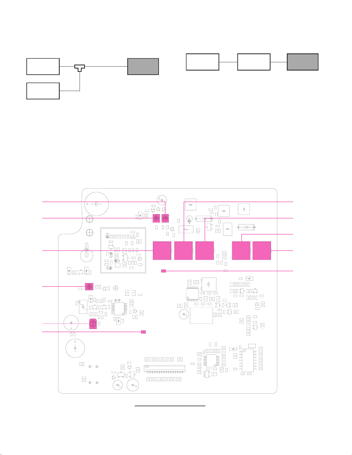
CNTL Unit
2.42 V (@13.8 V)
5.0 V
2.5 V
TX HI: 4.2 V
TX LOW: 0.6 V
CONT "1": 2.7 V
CONT "7": 4.7 V
12.0 V
DIM "1": 3.5 V
DIM "7": 4.9 V
DIM "1": 2.9 V
DIM "7": 4.3 V
Circuit Diagram
DIM "1": 5.7 V
DIM "7": 8.5 V
DIM "1": 5.4 V
DIM "7": 5.9 V
13.8 V
POWER "ON": 13.8 V
SQL "OPEN": 0 V
SQL "TH": 1.0 V
SQL "TI": 5.0 V
5.0 V
5.0 V
KEY BEEP: 440 mVp-p
WA LEVEL "Small": 450 mVp-p
WA LEVEL "Medium": 940 mVp-p
DSC
5.0 V
3.6 Vp-p
2.5 Vp-p
PTT "ON": 0 V
PTT "OFF": 5.0 V
KEY "OFF": 5.0 V
NMEA OUT: 4.9 Vp-p
5.0 V
5.0 V
25
Page 26

CNTL Unit
Parts Layout
BA DC E
1
2
1
2
ba dc e
3
3
(Side A) (Side B)
UPD78F0395GC
(Q2004)
2SA1602A (MF)
(Q2015, 2017, 2019)
ISA1602A (MF)
(Q2015, 2017, 2019)
BR24L08FVT
(Q2006)
2SB1132 (BA)
(Q2008)
DTA143ZE (E13)
(Q2001)
2SC4154 (LE)
(Q2007)
PST597CNR (7C)
(Q2003)
IMN10 (N10)
(D2002)
26
Page 27

CNTL Unit
Parts List
REF DESCRIPTION VALUE V/W TOL. MFR'S DESIG VXSTD P/N VERS.
P.C.B. with Components CS1984401 w/VR UNIT
Printed Circuit Board AM030N000 FR0175300 1C 2007 CHIP CAP. 0.001uF 25V CH GRM1882C1E102JA01D K22144204 1- B c1
C 2027 CHIP CAP. 0.1uF 25V F GRM188F11E104ZA01D K22145001 1- B c2
C 2028 CHIP CAP. 0.01uF 50V B GRM188B11H103KA01D K22174823 1- B c2
C 2029 CHIP CAP. 0.01uF 50V B GRM188B11H103KA01D K22174823 1- B d2
C 2030 CHIP CAP. 0.001uF 50V B GRM188B11H102KA01D K22174821 1- B d2
C 2031 CHIP CAP. 0.01uF 50V B GRM188B11H103KA01D K22174823 1- B b2
C 2032 CHIP CAP. 1uF 16V B C1608JB1C105KT K22124813 1- B b2
C 2033 CHIP CAP. 100pF 50V CH GRM1882C1H101JA01D K22174235 1- B d2
C 2034 CHIP CAP. 1uF 16V B C1608JB1C105KT K22124813 1- B b3
C 2035 CHIP CAP. 22pF 50V CH GRM1882C1H220JA01D K22174219 1- B b1
C 2036 CHIP CAP. 27pF 50V CH GRM1882C1H270JA01D K22174221 1- B b1
C 2037 CHIP TA.CAP. 10uF 10V F931A106MAA K78100078 1- B a1
C 2038 CHIP CAP. 0.01uF 50V B GRM188B11H103KA01D K22174823 1- B b2
C 2039 CHIP CAP. 1uF 16V B C1608JB1C105KT K22124813 1- B b1
C 2040 CHIP CAP. 0.01uF 50V B GRM188B11H103KA01D K22174823 1- B b1
C 2041 CHIP CAP. 1uF 16V B C1608JB1C105KT K22124813 1- B b2
C 2042 CHIP CAP. 0.01uF 50V B GRM188B11H103KA01D K22174823 1- B b1
C 2044 CHIP TA.CAP. 10uF 10V F931A106MAA K78100078 1- B c1
C 2045 CHIP CAP. 0.47uF 6.3V B GRM155B30J474KE18D K22088802 1- B a1
C 2046 CHIP CAP. 0.01uF 50V B GRM188B11H103KA01D K22174823 1- B b1
C 2049 CHIP CAP. 0.1uF 25V F GRM188F11E104ZA01D K22145001 1- B d1
C 2050 CHIP CAP. 0.1uF 25V F GRM188F11E104ZA01D K22145001 1- B d2
C 2053 CHIP CAP. 0.01uF 50V B GRM188B11H103KA01D K22174823 1- B d2
C 2054 CHIP CAP. 0.01uF 50V B GRM188B11H103KA01D K22174823 1- B d2
C 2055 CHIP CAP. 0.01uF 50V B GRM188B11H103KA01D K22174823 1- B d2
C 2056 CHIP CAP. 0.01uF 50V B GRM188B11H103KA01D K22174823 1- B d2
C 2057 CHIP CAP. 0.01uF 50V B GRM188B11H103KA01D K22174823 1- B d2
C 2065 CHIP CAP. 0.1uF 16V B GRM188B11C104KA01D K22124805 1- B a1
C 2066 CHIP CAP. 0.1uF 16V B GRM188B11C104KA01D K22124805 1- B d2
C 2067 CHIP CAP. 0.001uF 50V B GRM188B11H102KA01D K22174821 1- B b1
D 2001 DIODE 1SS355(TAPE) G2071200 1- B d2
D 2002 DIODE IMN10 T108 G2070078 1- B c1
D 2003 LED SML-512WWT86 G2071104 1- A D2
D 2004 LED SML-512WWT86 G2071104 1- A D2
D 2005 LED SML-512WWT86 G2071104 1- A D1
D 2006 LED SML-512WWT86 G2071104 1- A A1
D 2007 LED SML-512WWT86 G2071104 1- A A3
D 2008 LED SML-512WWT86 G2071104 1- A B2
DS2001 LCD DTE105978BKZ G6090184 1- A C1
FB2001 FERRITE BEADS BK1608HS601-T L9190083 1- B d3
FB2002 FERRITE BEADS BK1608HS601-T L9190083 1- B d2
FB2003 FERRITE BEADS BK1608HS601-T L9190083 1- B d3
J 2001 CONNECTOR 32FLT-SM2-TB(LF)(SN) P1091258 1- B c1
J 2002 CONNECTOR A2001WV-S-03PD01 P0091502 1- B d3
J 2003 CONNECTOR AXK6F10345YP P0091378 1- B c3
J 2004 CONNECTOR A2001WV-S-04PD01 P0091504 1- B d3
Q 2001 TRANSISTOR DTA143ZE TL G3070390 1- B c2
Q 2002 PHOTO COUPLER PC3H7CDJ000F G0090039 1- B d2
Q 2003 IC PST597CNR G1092589 1- B d2
Q 2004 IC UPD78F0395GC-8EA-A G1094521 1- B b2
Q 2006 IC BR24L08FVT-W(TAPE) G1094519 1- B c1
Q 2007 TRANSISTOR 2SC4154-T11-1E G3341548E 1- B d2
Q 2008 TRANSISTOR 2SB1132 T100 R G3211327R 1- B d1
R 2001 CHIP RES. 150 1/2W 5% RK73K2HTE150-J J24279019 1- B d3
R 2002 CHIP RES. 330 1/4W 5% RMC1/4 331JATP J24245331 1- B d2
R 2003 CHIP RES. 22k 1/16W 5% RMC1/16 223JATP J24185223 1- B c2
R 2004 CHIP RES. 47k 1/16W 5% RMC1/16 473JATP J24185473 1- B c2
R 2005 CHIP RES. 100k 1/16W 5% RMC1/16 104JATP J24185104 1- B c2
R 2006 CHIP RES. 47k 1/16W 5% RMC1/16 473JATP J24185473 1- B c2
R 2007 CHIP RES. 100k 1/16W 5% RMC1/16 104JATP J24185104 1- B c2
R 2008 CHIP RES. 100k 1/16W 5% RMC1/16 104JATP J24185104 1- B c2
R 2009 CHIP RES. 3.9k 1/16W 5% RMC1/16 392JATP J24185392 1- B d2
R 2010 CHIP RES. 0 1/16W 5% RMC1/16 000JATP J24185000 1- B c2
R 2011 CHIP RES. 0 1/16W 5% RMC1/16 000JATP J24185000 1- B b2
R 2012 CHIP RES. 0 1/16W 5% RMC1/16 000JATP J24185000 1- B c2
R 2013 CHIP RES. 0 1/16W 5% RMC1/16 000JATP J24185000 1- B b2
R 2014 CHIP RES. 0 1/16W 5% RMC1/16 000JATP J24185000 1- B c2
R 2015 CHIP RES. 0 1/16W 5% RMC1/16 000JATP J24185000 1- B b2
R 2016 CHIP RES. 0 1/16W 5% RMC1/16 000JATP J24185000 1- B c2
R 2017 CHIP RES. 0 1/16W 5% RMC1/16 000JATP J24185000 1- B b2
R 2018 CHIP RES. 10k 1/16W 5% RMC1/16 103JATP J24185103 1- B c2
LOT
SIDE
LAY ADR
27
Page 28

CNTL Unit
Parts List
REF DESCRIPTION VALUE V/W TOL. MFR'S DESIG VXSTD P/N VERS.
R 2019 CHIP RES. 22k 1/16W 5% RMC1/16 223JATP J24185223 1- B b2
R 2020 CHIP RES. 47k 1/16W 5% RMC1/16 473JATP J24185473 1- B c2
R 2021 CHIP RES. 100k 1/16W 5% RMC1/16 104JATP J24185104 1- B b2
R 2022 CHIP RES. 220k 1/16W 5% RMC1/16 224JATP J24185224 1- B c2
R 2023 CHIP RES. 4.7k 1/16W 5% RMC1/16 472JATP J24185472 1- B b2
R 2024 CHIP RES. 0 1/16W 5% RMC1/16 000JATP J24185000 1- B c1
R 2025 CHIP RES. 0 1/16W 5% RMC1/16 000JATP J24185000 1- B b1
R 2026 CHIP RES. 0 1/16W 5% RMC1/16 000JATP J24185000 1- B b1
R 2027 CHIP RES. 0 1/16W 5% RMC1/16 000JATP J24185000 1- B b1
R 2028 CHIP RES. 10k 1/16W 5% RMC1/16 103JATP J24185103 1- B d2
R 2029 CHIP RES. 10k 1/16W 5% RMC1/16 103JATP J24185103 1- B b1
R 2030 CHIP RES. 220 1/16W 5% RMC1/16 221JATP J24185221 1- B b1
R 2031 CHIP RES. 0 1/16W 5% RMC1/16 000JATP J24185000 1- B b2
R 2032 CHIP RES. 0 1/16W 5% RMC1/16 000JATP J24185000 1- B c2
R 2034 CHIP RES. 470 1/16W 5% RMC1/16 471JATP J24185471 1- B d2
R 2035 CHIP RES. 100 1/16W 5% RMC1/16 101JATP J24185101 1- B b2
R 2036 CHIP RES. 100 1/16W 5% RMC1/16 101JATP J24185101 1- B c2
R 2037 CHIP RES. 10k 1/16W 5% RMC1/16 103JATP J24185103 1- B b2
R 2038 CHIP RES. 10k 1/16W 5% RMC1/16 103JATP J24185103 1- B b2
R 2039 CHIP RES. 0 1/16W 5% RMC1/16 000JATP J24185000 1- B b1
R 2040 CHIP RES. 0 1/16W 5% RMC1/16 000JATP J24185000 1- B b1
R 2041 CHIP RES. 0 1/16W 5% RMC1/16 000JATP J24185000 1- B b2
R 2042 CHIP RES. 470 1/16W 5% RMC1/16 471JATP J24185471 1- B b1
R 2043 CHIP RES. 0 1/16W 5% RMC1/16 000JATP J24185000 1- B b2
R 2045 CHIP RES. 100 1/16W 5% RMC1/16 101JATP J24185101 1- B b2
R 2046 CHIP RES. 0 1/16W 5% RMC1/16 000JATP J24185000 1- B b1
R 2048 CHIP RES. 0 1/16W 5% RMC1/16 000JATP J24185000 1- B b3
R 2051 CHIP RES. 0 1/16W 5% RMC1/16 000JATP J24185000 1- B a2
R 2055 CHIP RES. 4.7k 1/16W 5% RMC1/16 472JATP J24185472 1- B b1
R 2056 CHIP RES. 4.7k 1/16W 5% RMC1/16 472JATP J24185472 1- B b1
R 2057 CHIP RES. 39 1/4W 5% RMC1/4 390JATP J24245390 1- B d1
R 2058 CHIP RES. 470k 1/16W 5% RMC1/16 474JATP J24185474 1- B d2
R 2059 CHIP RES. 470 1/16W 5% RMC1/16 471JATP J24185471 1- B d2
R 2060 CHIP RES. 10k 1/16W 5% RMC1/16 103JATP J24185103 1- B d2
R 2061 CHIP RES. 1k 1/16W 5% RMC1/16 102JATP J24185102 1- B d2
R 2062 CHIP RES. 2.2k 1/16W 5% RMC1/16 222JATP J24185222 1- B d1
R 2063 CHIP RES. 470 1/16W 5% RMC1/16 471JATP J24185471 1- B d2
R 2064 CHIP RES. 470 1/16W 5% RMC1/16 471JATP J24185471 1- B d2
R 2065 CHIP RES. 470 1/16W 5% RMC1/16 471JATP J24185471 1- B d2
R 2066 CHIP RES. 150 1/10W 5% RMC1/10T 151J J24205151 1- B d1
R 2067 CHIP RES. 150 1/10W 5% RMC1/10T 151J J24205151 1- B d1
R 2068 CHIP RES. 0 1/16W 5% RMC1/16 000JATP J24185000 1- B d2
R 2069 CHIP RES. 2.2k 1/16W 5% RMC1/16 222JATP J24185222 1- B d3
R 2070 CHIP RES. 10k 1/16W 5% RMC1/16 103JATP J24185103 1- B c1
X 2001 XTAL HC-49/SS-SMD 18.432MHz 18.432MHZ H0103369 1- B b1
LIGHT GUIDE (LCD) RA0975100 1INTER CONNECTOR (LCD) RA0975400 1REFLECTOR SHEET (LCD) RA0975500 1SPONGE RUBBER (LCD) RA0975200 1-
LOT
SIDE
LAY ADR
28
Page 29

MIC Unit
Circuit Diagram
Parts Layout
(Side A) (Side B)
Parts List
REF DESCRIPTION VALUE V/W TOL. MFR'S DESIG VXSTD P/N VERS.
Printed Circuit Board AM030N000 FR017990C 1C 3502 CERAMIC CAP. 0.001uF 50V B BU5 102K6(5MM) K10179056 1- B a2
MC3501 MIC. ELEMENT EM-100PT M3290029 1- B b3
S 3501 TACT SWITCH SKHLLD N5090066 1- B a1
LOT
SIDE
LAY ADR
29
Page 30

VR Unit
Parts Layout
Parts Layout
(Side B)(Side A)
Parts List
REF DESCRIPTION VALUE V/W TOL. MFR'S DESIG VXSTD P/N VERS.
Printed Circuit Board AM030N000 FR0176800 1J 3001 CONNECTOR 21B12050-07S10B01G3.5/3.5 P0091505 1- B a1
VR3001 POT. WH9011AK-1-34D15/5H=5A20K J60800294 1- A A1
VR3002 POT. WH9011A-1-40D15/5H=5B20K J60800295 1- A A2
30
LOT
SIDE
LAY ADR
Page 31

31
Page 32

Copyright 2008
VERTEX STANDARD CO., LTD.
All rights reserved
No portion of this manual
may be reproduced without
the permission of
VERTEX STANDARD CO., LTD.
32
 Loading...