

Features
VND5E004A-E
VND5E004ASP30-E
Double 4mΩ high-side driver with analog current sense
for automotive applications
Max transient supply voltage V
Operating voltage range V
Max on-state resistance (per ch.) R
Current limitation (typ) I
Off-state supply current I
1. Typical value with all loads connected
■ General
CC
CC
ON
LIMH
S
4.5 to 28 V
– Very low standby current
– 3.0 V CMOS compatible inputs
– Optimized electromagnetic emissions
– Very low electromagnetic susceptibility
– Compliant with European directive
2002/95/EC
– Very low current sense leakage
■ Diagnostic functions
– Proportional load current sense
– High current sense precision for wide
currents range
– Diagnostic enable pin
– Off-state open-load detection
– Output short to V
detection
CC
– Overload and short to ground (power
limitation) indication
– Thermal shutdown indication
■ Protection
– Undervoltage shutdown
– Overvoltage clamp
– Load current limitation
– Self limiting of fast thermal transients
– Protection against loss of ground and loss
of V
CC
– Overtemperature shutdown with auto
restart (thermal shutdown)
– Inrush current active management by
power limitation
41 V
4mΩ
90 A
2µA
(1)
MultiPowerSO-30PQFN - 12x12 Power lead-less
– Reverse battery protection with self switch
on of the Power MOSFET
– Electrostatic discharge protection
Applications
■ All types of resistive, inductive and capacitive
loads
■ Suitable for power management applications
Description
The VND5E004A-E and VND5E004ASP30-E are
double channel high-side drivers manufactured
using ST proprietary VIPower™ M0-5 technology
and housed in PQFN-12x12 power lead-less and
MultiPowerSO-30 packages. The devices are
designed to drive 12 V automotive grounded
loads, and to provide protection and diagnostics.
They also implement a 3 V and 5 V CMOScompatible interface for use with any
microcontroller.
The devices integrate advanced protective
functions such as load current limitation, inrush
and overload active management by power
limitation, overtemperature shut-off with autorestart and overvoltage active clamp. A dedicated
analog current sense pin is associated with every
output channel providing enhanced diagnostic
functions including fast detection of overload and
short-circuit to ground through power limitation
indication, overtemperature indication, shortcircuit to V
open-load detection. The current sensing and
diagnostic feedback of the whole device can be
disabled by pulling the DE pin low to share the
external sense resistor with similar devices.
diagnosis and on-state and off-state
CC
July 2010 Doc ID 17359 Rev 1 1/45
www.st.com
1

Contents VND5E004A-E / VND5E004ASP30-E
Contents
1 Block diagram and pin configurations . . . . . . . . . . . . . . . . . . . . . . . . . . 6
2 Electrical specifications . . . . . . . . . . . . . . . . . . . . . . . . . . . . . . . . . . . . . . 8
2.1 Absolute maximum ratings . . . . . . . . . . . . . . . . . . . . . . . . . . . . . . . . . . . . . 8
2.2 Thermal data . . . . . . . . . . . . . . . . . . . . . . . . . . . . . . . . . . . . . . . . . . . . . . . 9
2.3 Electrical characteristics . . . . . . . . . . . . . . . . . . . . . . . . . . . . . . . . . . . . . . 10
2.4 Waveforms . . . . . . . . . . . . . . . . . . . . . . . . . . . . . . . . . . . . . . . . . . . . . . . . 19
2.5 Electrical characteristics curves . . . . . . . . . . . . . . . . . . . . . . . . . . . . . . . . 22
3 Application information . . . . . . . . . . . . . . . . . . . . . . . . . . . . . . . . . . . . . 25
3.1 MCU I/Os protection . . . . . . . . . . . . . . . . . . . . . . . . . . . . . . . . . . . . . . . . . 25
3.2 Load dump protection . . . . . . . . . . . . . . . . . . . . . . . . . . . . . . . . . . . . . . . . 25
3.3 Current sense and diagnostic . . . . . . . . . . . . . . . . . . . . . . . . . . . . . . . . . . 26
3.3.1 Short to VCC and off-state open-load detection . . . . . . . . . . . . . . . . . . 27
3.4 Maximum demagnetization energy (VCC = 13.5V) . . . . . . . . . . . . . . . . . 29
4 Package and PC board thermal data . . . . . . . . . . . . . . . . . . . . . . . . . . . 30
4.1 MultiPowerSO-30 thermal data . . . . . . . . . . . . . . . . . . . . . . . . . . . . . . . . 30
4.2 PQFN - 12x12 power lead-less thermal data . . . . . . . . . . . . . . . . . . . . . . 33
5 Package and packing information . . . . . . . . . . . . . . . . . . . . . . . . . . . . . 36
5.1 ECOPACK® packages . . . . . . . . . . . . . . . . . . . . . . . . . . . . . . . . . . . . . . . 36
5.2 MultiPowerSO-30 mechanical data . . . . . . . . . . . . . . . . . . . . . . . . . . . . . 36
5.3 PQFN - 12x12 power lead-less mechanical data . . . . . . . . . . . . . . . . . . . 38
5.4 MultiPowerSO-30 packing information . . . . . . . . . . . . . . . . . . . . . . . . . . . 40
5.5 PQFN - 12x12 power lead-less packing information . . . . . . . . . . . . . . . . 41
6 Order codes . . . . . . . . . . . . . . . . . . . . . . . . . . . . . . . . . . . . . . . . . . . . . . . 43
7 Revision history . . . . . . . . . . . . . . . . . . . . . . . . . . . . . . . . . . . . . . . . . . . 44
2/45 Doc ID 17359 Rev 1

VND5E004A-E / VND5E004ASP30-E List of tables
List of tables
Table 1. Pin functions . . . . . . . . . . . . . . . . . . . . . . . . . . . . . . . . . . . . . . . . . . . . . . . . . . . . . . . . . . . . . 6
Table 2. Suggested connections for unused and not connected pins . . . . . . . . . . . . . . . . . . . . . . . . 7
Table 3. Absolute maximum ratings . . . . . . . . . . . . . . . . . . . . . . . . . . . . . . . . . . . . . . . . . . . . . . . . . . 8
Table 4. Thermal data. . . . . . . . . . . . . . . . . . . . . . . . . . . . . . . . . . . . . . . . . . . . . . . . . . . . . . . . . . . . . 9
Table 5. Power section . . . . . . . . . . . . . . . . . . . . . . . . . . . . . . . . . . . . . . . . . . . . . . . . . . . . . . . . . . . 10
Table 6. Switching (VCC = 13 V; Tj = 25 °C) . . . . . . . . . . . . . . . . . . . . . . . . . . . . . . . . . . . . . . . . . . 11
Table 7. Logic inputs. . . . . . . . . . . . . . . . . . . . . . . . . . . . . . . . . . . . . . . . . . . . . . . . . . . . . . . . . . . . . 11
Table 8. Protections and diagnostics . . . . . . . . . . . . . . . . . . . . . . . . . . . . . . . . . . . . . . . . . . . . . . . . 12
Table 9. Current sense (8 V < V
Table 10. Open-load detection (8V<V
Table 11. Truth table. . . . . . . . . . . . . . . . . . . . . . . . . . . . . . . . . . . . . . . . . . . . . . . . . . . . . . . . . . . . . . 17
Table 12. Electrical transient requirements (part 1/3) . . . . . . . . . . . . . . . . . . . . . . . . . . . . . . . . . . . . . 18
Table 13. Electrical transient requirements (part 2/3) . . . . . . . . . . . . . . . . . . . . . . . . . . . . . . . . . . . . . 18
Table 14. Electrical transient requirements (part 3/3) . . . . . . . . . . . . . . . . . . . . . . . . . . . . . . . . . . . . . 18
Table 15. Thermal parameters for MultiPowerSO-30 . . . . . . . . . . . . . . . . . . . . . . . . . . . . . . . . . . . . . 32
Table 16. Thermal parameters for PQFN - 12x12 power lead-less . . . . . . . . . . . . . . . . . . . . . . . . . . 35
Table 17. MultiPowerSO-30 mechanical data . . . . . . . . . . . . . . . . . . . . . . . . . . . . . . . . . . . . . . . . . . 37
Table 18. PQFN - 12x12 power lead-less mechanical data . . . . . . . . . . . . . . . . . . . . . . . . . . . . . . . . 39
Table 19. Device summary . . . . . . . . . . . . . . . . . . . . . . . . . . . . . . . . . . . . . . . . . . . . . . . . . . . . . . . . . 43
Table 20. Document revision history . . . . . . . . . . . . . . . . . . . . . . . . . . . . . . . . . . . . . . . . . . . . . . . . . 44
< 18 V) . . . . . . . . . . . . . . . . . . . . . . . . . . . . . . . . . . . . . . . . . . . 12
CC
<18V, VDE= 5V) . . . . . . . . . . . . . . . . . . . . . . . . . . . . . . . . . 14
CC
Doc ID 17359 Rev 1 3/45

List of figures VND5E004A-E / VND5E004ASP30-E
List of figures
Figure 1. Block diagram . . . . . . . . . . . . . . . . . . . . . . . . . . . . . . . . . . . . . . . . . . . . . . . . . . . . . . . . . . . . 6
Figure 2. Configuration diagram (not in scale). . . . . . . . . . . . . . . . . . . . . . . . . . . . . . . . . . . . . . . . . . . 7
Figure 3. Current and voltage conventions . . . . . . . . . . . . . . . . . . . . . . . . . . . . . . . . . . . . . . . . . . . . . 8
Figure 4. Current sense delay characteristics . . . . . . . . . . . . . . . . . . . . . . . . . . . . . . . . . . . . . . . . . . 14
Figure 5. Open-load off-state delay timing. . . . . . . . . . . . . . . . . . . . . . . . . . . . . . . . . . . . . . . . . . . . . 14
Figure 6. Switching characteristics . . . . . . . . . . . . . . . . . . . . . . . . . . . . . . . . . . . . . . . . . . . . . . . . . . 15
Figure 7. Delay response time between rising edge of output current and rising edge of current sense
(CS enabled) . . . . . . . . . . . . . . . . . . . . . . . . . . . . . . . . . . . . . . . . . . . . . . . . . . . . . . . . . . . 15
Figure 8. Output voltage drop limitation . . . . . . . . . . . . . . . . . . . . . . . . . . . . . . . . . . . . . . . . . . . . . . . 16
Figure 9. I
OUT/ISENSE
Figure 10. Maximum current sense ratio drift vs load current
Figure 11. Normal operation . . . . . . . . . . . . . . . . . . . . . . . . . . . . . . . . . . . . . . . . . . . . . . . . . . . . . . . . 19
Figure 12. Overload or short to GND . . . . . . . . . . . . . . . . . . . . . . . . . . . . . . . . . . . . . . . . . . . . . . . . . . 19
Figure 13. Intermittent overload . . . . . . . . . . . . . . . . . . . . . . . . . . . . . . . . . . . . . . . . . . . . . . . . . . . . . . 20
Figure 14. Off-state open-load with external circuitry . . . . . . . . . . . . . . . . . . . . . . . . . . . . . . . . . . . . . 20
Figure 15. Short to V
Figure 16. T
evolution in overload or short to GND . . . . . . . . . . . . . . . . . . . . . . . . . . . . . . . . . . . . . . 21
J
Figure 17. Off-state output current. . . . . . . . . . . . . . . . . . . . . . . . . . . . . . . . . . . . . . . . . . . . . . . . . . . . 22
Figure 18. High level input current . . . . . . . . . . . . . . . . . . . . . . . . . . . . . . . . . . . . . . . . . . . . . . . . . . . . 22
Figure 19. Input clamp voltage. . . . . . . . . . . . . . . . . . . . . . . . . . . . . . . . . . . . . . . . . . . . . . . . . . . . . . . 22
Figure 20. Input low level voltage . . . . . . . . . . . . . . . . . . . . . . . . . . . . . . . . . . . . . . . . . . . . . . . . . . . . 22
Figure 21. Input high level voltage . . . . . . . . . . . . . . . . . . . . . . . . . . . . . . . . . . . . . . . . . . . . . . . . . . . . 22
Figure 22. Input hysteresis voltage . . . . . . . . . . . . . . . . . . . . . . . . . . . . . . . . . . . . . . . . . . . . . . . . . . . 22
Figure 23. On-state resistance vs T
Figure 24. On-state resistance vs V
Figure 25. Undervoltage shutdown . . . . . . . . . . . . . . . . . . . . . . . . . . . . . . . . . . . . . . . . . . . . . . . . . . . 23
Figure 26. Turn-on voltage slope . . . . . . . . . . . . . . . . . . . . . . . . . . . . . . . . . . . . . . . . . . . . . . . . . . . . . 23
Figure 27. I
LIMH
vs T
Figure 28. Turn-off voltage slope . . . . . . . . . . . . . . . . . . . . . . . . . . . . . . . . . . . . . . . . . . . . . . . . . . . . . 23
Figure 29. DE high level voltage . . . . . . . . . . . . . . . . . . . . . . . . . . . . . . . . . . . . . . . . . . . . . . . . . . . . . 24
Figure 30. DE clamp voltage . . . . . . . . . . . . . . . . . . . . . . . . . . . . . . . . . . . . . . . . . . . . . . . . . . . . . . . . 24
Figure 31. DE low level voltage . . . . . . . . . . . . . . . . . . . . . . . . . . . . . . . . . . . . . . . . . . . . . . . . . . . . . . 24
Figure 32. Application schematic . . . . . . . . . . . . . . . . . . . . . . . . . . . . . . . . . . . . . . . . . . . . . . . . . . . . 25
Figure 33. Current sense and diagnostics . . . . . . . . . . . . . . . . . . . . . . . . . . . . . . . . . . . . . . . . . . . . . 27
Figure 34. Maximum turn-off current versus inductance
Figure 35. MultiPowerSO-30 PC board
Figure 36. Rthj-amb vs PCB copper area in open box free air condition (one channel ON) . . . . . . . . 30
Figure 37. MultiPowerSO-30 thermal impedance junction ambient single pulse (one channel ON) . . 31
Figure 38. Thermal fitting model of a double channel HSD in MultiPowerSO-30
Figure 39. 12x12 Power lead-less package PC board
Figure 40. Rthj-amb vs PCB copper area in open box free air condition (one channel ON) . . . . . . . . 33
Figure 41. PQFN - 12x12 power lead-less package thermal impedance junction ambient single pulse
(one channel ON) . . . . . . . . . . . . . . . . . . . . . . . . . . . . . . . . . . . . . . . . . . . . . . . . . . . . . . . . 34
Figure 42. Thermal fitting model of a double channel HSD in PQFN - 12x12 power lead-less
Figure 43. MultiPowerSO-30 outline . . . . . . . . . . . . . . . . . . . . . . . . . . . . . . . . . . . . . . . . . . . . . . . . . . 36
Figure 44. PQFN - 12x12 power lead-less outline . . . . . . . . . . . . . . . . . . . . . . . . . . . . . . . . . . . . . . . . 38
Figure 45. MultiPowerSO-30 tube shipment (no suffix) . . . . . . . . . . . . . . . . . . . . . . . . . . . . . . . . . . . 40
Figure 46. MultiPowerSO-30 tape and reel shipment (suffix “TR”) . . . . . . . . . . . . . . . . . . . . . . . . . . . 40
vs I
. . . . . . . . . . . . . . . . . . . . . . . . . . . . . . . . . . . . . . . . . . . . . . . . . . . . . . . . . . . . 21
CC
case
. . . . . . . . . . . . . . . . . . . . . . . . . . . . . . . . . . . . . . . . . . . . . . . . . . . . . . 16
OUT
. . . . . . . . . . . . . . . . . . . . . . . . . . . . . . . . . . . . . . . . . . . . . . . . 23
case
. . . . . . . . . . . . . . . . . . . . . . . . . . . . . . . . . . . . . . . . . . . . . . . . . 23
CC
(1)
. . . . . . . . . . . . . . . . . . . . . . . . . . . . . 17
. . . . . . . . . . . . . . . . . . . . . . . . . . . . . . . . . . . . . . . . . . . . . . . . . . . . . . . . . . . 23
(1)
(1)
. . . . . . . . . . . . . . . . . . . . . . . . . . . . . . . . . . . . . . . . . . . . . . 30
. . . . . . . . . . . . . . . . . . . . . . . . . . . . . . . . . 29
(1)
(1)
. . . . . . . . . . . . . . . . . . . . . . . . . . . . . . . . . . . 33
. . . . . . . . . . . . . . 31
(1)
. . . . 34
4/45 Doc ID 17359 Rev 1

VND5E004A-E / VND5E004ASP30-E List of figures
Figure 47. PQFN - 12x12 power lead-less tray shipment (no suffix) . . . . . . . . . . . . . . . . . . . . . . . . . . 41
Figure 48. PQFN - 12x12 power lead-less tape and reel shipment (suffix “TR”) . . . . . . . . . . . . . . . . . 42
Doc ID 17359 Rev 1 5/45
Block diagram and pin configurations VND5E004A-E / VND5E004ASP30-E
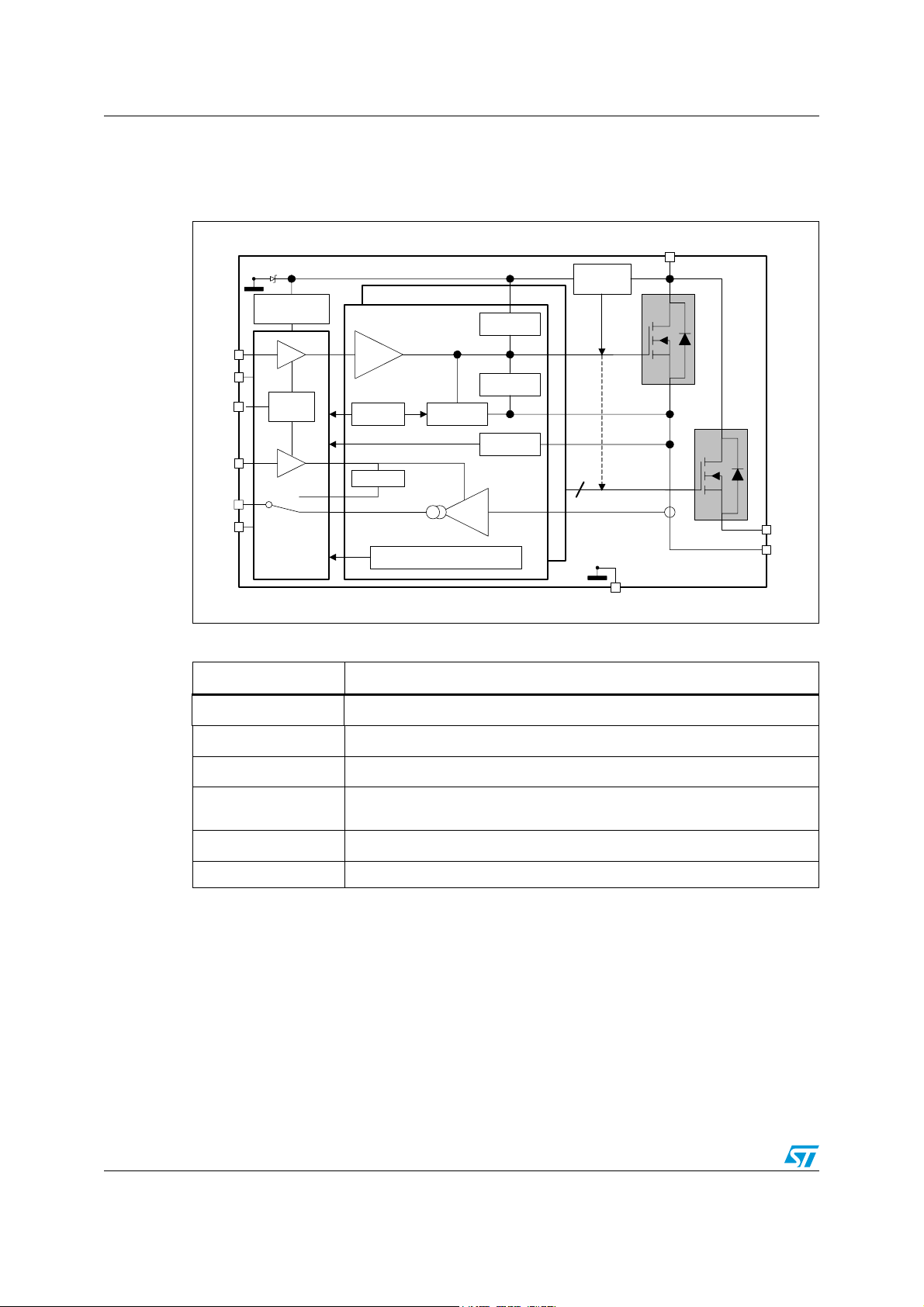
1 Block diagram and pin configurations
Figure 1. Block diagram
V
CC
Reverse
Battery
Protection
CH 1
CH 2
OUT2
OUT1
IN1
IN2
CE
CS_
DIS
CS1
CS2
Signal Clamp
Undervoltage
Device
Enable
LOGIC
Control & Diagnostic 2
Control & Diagnostic 1
DRIVER
Over
temp.
V
SENSEH
OVERLOAD P ROTECTION
(ACTIVE POWER LIMITATION)
Current
Limitation
Current
Sense
Power
Clamp
V
ON
Limitation
OFF State
Open load
Table 1. Pin functions
Name Function
V
CC
Battery connection
OUT1,2 Power output
GND Ground connection
IN1,2
Voltage controlled input pin with hysteresis, CMOS compatible, controls
output switch state
CS1,2 Analog current sense pin; delivers a current proportional to the load current
DE Active high diagnostic enable pin
GND
6/45 Doc ID 17359 Rev 1
VND5E004A-E / VND5E004ASP30-E Block diagram and pin configurations
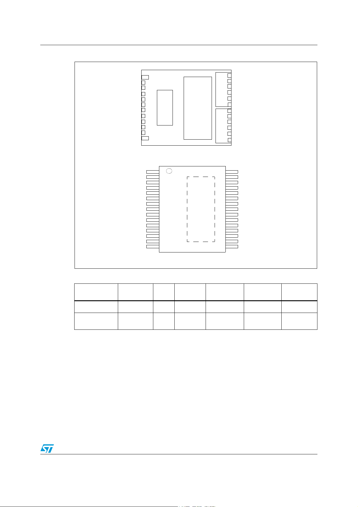
Figure 2. Configuration diagram (not in scale)
1 NC
2 NC
3 NC
4 GND
5 DE
6 CS 1
7 CS 2
8 IN 1
9 IN 2
10 NC
11 NC
12 NC
13 FOR TEST ONLY
14 V
CC
15 OUT 2
PQFN -12x12 Power
lead-less
(bottom view)
11
10
9
8
7
6
5
4
3
2
12
1
13
15
14
16
16 OUT 1
V
CC
NC
1
FOR TEST ONLY
NC
NC
GND
DE
CS 1
CS 2
IN 1
V
CC
Heat Slug1
IN 2
NC
FOR TEST ONLY
NC
V
CC
Table 2. Suggested connections for unused and not connected pins
Connection /
pin
Current
sense
15 16
(1)
NC
Output Input DE For test only
30
V
CC
OUT 1
OUT 1
OUT 1
OUT 1
OUT 1
OUT 1
NC
OUT 2
OUT 2
MultiPowerSO-30
OUT 2
OUT 2
OUT 2
OUT 2
V
CC
Floating Not allowed X X X X X
To ground
1. Not connected
Through 1kΩ
resistor
X
Not
allowed
Through 10kΩ
resistor
Through
10kΩ resistor
(top view)
Not allowed
Doc ID 17359 Rev 1 7/45
Electrical specifications VND5E004A-E / VND5E004ASP30-E
2 Electrical specifications
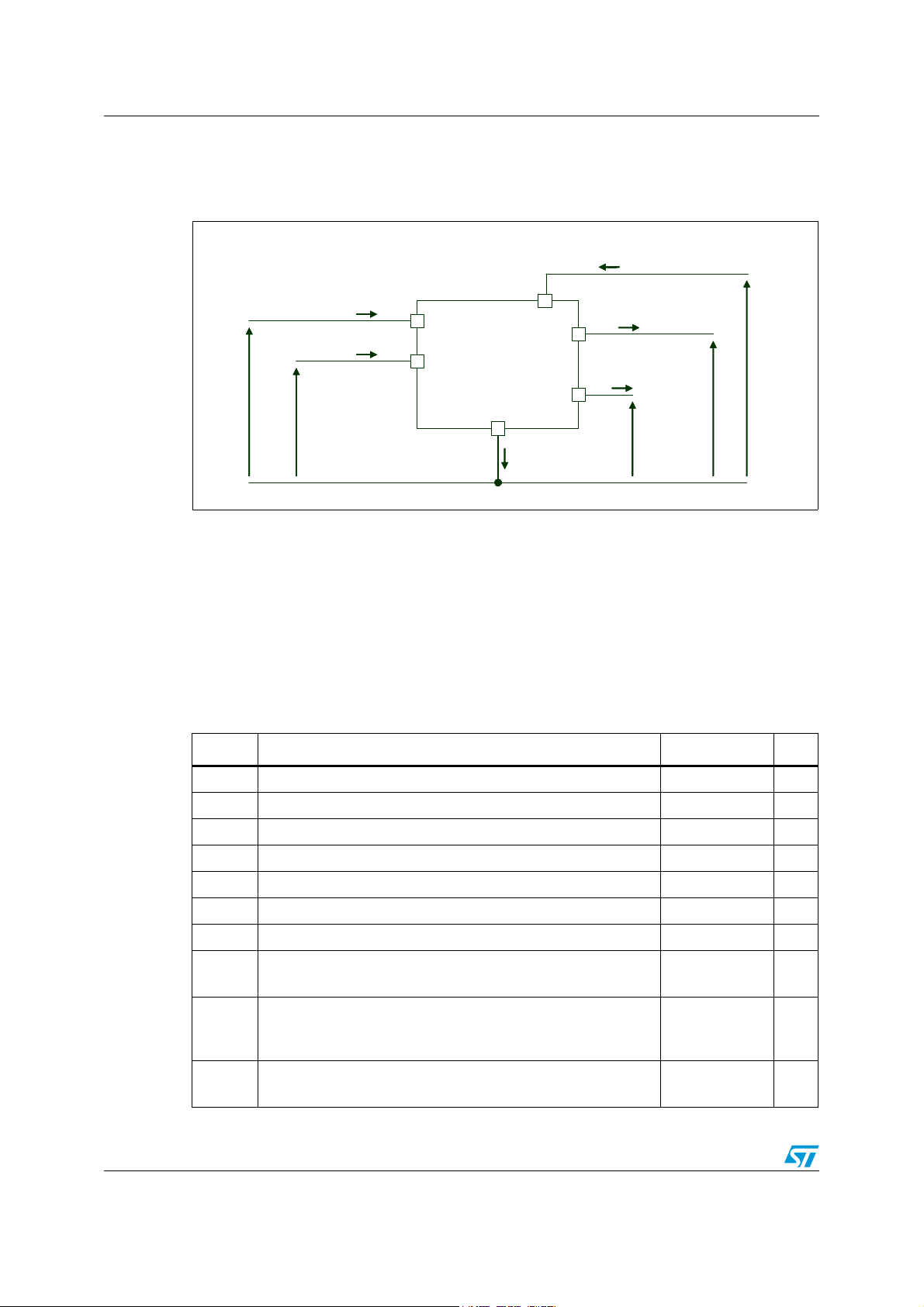
Figure 3. Current and voltage conventions
I
I
S
S
V
V
CC
GND
GND
CC
OUTPUT1,2
OUTPUT1,2
CURRENT
CURRENT
SENSE1,2
SENSE1,2
I
I
GND
GND
I
I
OUT1,2
OUT1,2
I
I
SENSE1,2
SENSE1,2
V
V
SENSE1,2
SENSE1,2
V
V
OUT1,2
OUT1,2
I
I
DE
DE
DE
DE
I
I
IN1,2
IN1,2
IN1,2
IN1,2
INPUT1,2
INPUT1,2
V
V
DE
DE
V
V
V
V
CC
CC
2.1 Absolute maximum ratings
Applying stress which exceeds above the ratings listed in Table 3: Absolute maximum
ratings may cause permanent damage to the device. These are stress ratings only and
operation of the device at these or any other conditions above those indicated in the
Operating sections of this specification is not implied. Exposure to the conditions in this
section for extended periods may affect device reliability. Refer also to the
STMicroelectronics SURE Program and other relevant quality documents.
Table 3. Absolute maximum ratings
Symbol Parameter Value Unit
V
V
CCPK
-V
I
OUT
- I
V
CSENSE
E
V
DC supply voltage 28 V
CC
Transient supply voltage (T < 400 ms, R
Reverse DC supply voltage 16 V
CC
DC output current Internally limited A
Reverse DC output current 70 A
OUT
I
DC input current -1 to 10 mA
IN
DC diagnostic enable input current -1 to 10 mA
I
DE
Current sense maximum voltage (VCC>0V)
Maximum switching energy (single pulse)
MAX
(L = 0.3 mH; R
I
OUT=IlimL
(Typ.))
=0Ω; V
L
=13.5V; T
bat
Electrostatic discharge
ESD
(Human Body Model: R = 1.5 kΩ; C=100pF)
>0.5Ω) 41 V
load
V
-41
CC
+V
CC
jstart
= 150 °C;
600 mJ
2000 V
V
V
8/45 Doc ID 17359 Rev 1
VND5E004A-E / VND5E004ASP30-E Electrical specifications
Table 3. Absolute maximum ratings (continued)
Symbol Parameter Value Unit
V
T
Charge device model (CDM-AEC-Q100-011) 750 V
ESD
T
Junction operating temperature -40 to 150 °C
j
Storage temperature -55 to 150 °C
STG
2.2 Thermal data
Table 4. Thermal data
Symbol Parameter
R
thj-case
R
thj-amb
1. PCB FR4 area 58 mm x 58 mm, PCB thickness 2 mm, Cu thickness 35 µm, minimum pad layout
2. PCB FR4 area 78 mm x 78 mm, PCB thickness 2 mm, Cu thickness 35 µm, minimum pad layout
Thermal resistance junction-case (with one
channel ON)
Thermal resistance junction-ambient 58
Maximum value
MultiPowerSO-30 12x12 PLLP
0.35 0.35 °C/W
(1)
39
(2)
Unit
°C/W
Doc ID 17359 Rev 1 9/45
Electrical specifications VND5E004A-E / VND5E004ASP30-E
2.3 Electrical characteristics
Values specified in this section are for 8 V < VCC<24V, -40°C <Tj<150°C, unless
otherwise stated.
Table 5. Power section
Symbol Parameter Test conditions Min. Typ. Max. Unit
V
V
V
USDhyst
R
R
ON REV
V
I
L(off)
1. For each channel
Operating supply voltage 4.5 13 28 V
CC
Undervoltage shutdown 3.5 4.5 V
USD
Undervoltage shutdown
hysteresis
On-state resistance
ON
R
DSon
condition
clampVCC
I
S
clamp voltage ICC=20mA; I
Supply current
Off-state output current
(1)
in reverse battery
I
=15A; Tj=25°C 3 mΩ
OUT
=15A; Tj= 150 °C 6 mΩ
I
OUT
I
=15A; VCC=5V; Tj=25°C 6 mΩ
OUT
VCC=-13V; I
=25°C
T
j
=-15A;
OUT
=0A 41 46 52 V
OUT1,2
Standby VDE=0V; VCC=13V;
=25°C; VIN=0;
T
j
V
OUT=VSENSE
Off-state; V
=5V; Tj=25°C;
V
DE
VIN=V
OUT=VSENSE
On-state; V
=5V; I
V
IN
=0V
=13V;
CC
=0V
=13V; VDE=5V;
CC
=0A
OUT
VIN=0V or VDE=0V; V
=13V; Tj= 25 °C 0 0.01 3 µA
V
CC
(1)
=0V or VDE=0V; V
V
IN
=13V; Tj=125°C
V
CC
OUT
OUT
=0V;
=0V;
0.5 V
3mΩ
25µA
10 15 µA
3.5 6 mA
05µA
10/45 Doc ID 17359 Rev 1
VND5E004A-E / VND5E004ASP30-E Electrical specifications
Table 6. Switching (VCC=13V; Tj=25°C)
Symbol Parameter Test conditions Min. Typ. Max. Unit
t
d(on)
t
d(off)
(dV
OUT
(dV
OUT
W
ON
W
OFF
Table 7. Logic inputs
Turn-on delay time RL= 0.87 Ω (see Ta bl e 6 )— 25 — µs
Turn-off delay time RL= 0.87 Ω (see Ta bl e 6 )— 35 — µs
/dt)onTurn-on voltage slope RL= 0.87 Ω —
/dt)
Turn-off voltage slope RL= 0.87 Ω —
off
Switching energy
losses during t
won
Switching energy
losses during t
woff
RL= 0.87 Ω (see Ta b le 6 )— 5.4 —mJ
RL= 0.87 Ω (see Ta b le 6)— 2.3 —mJ
See
Figure 26
See
Figure 28
—V/µs
—V/µs
Symbol Parameter Test conditions Min. Typ. Max. Unit
V
IL1,2
I
IL1,2
V
IH1,2
I
IH1,2
V
I(hyst)1,2
V
ICL1,2
V
DEL
I
DEL
V
DEH
I
DEH
V
DE(hyst)
V
DECL
Input low level voltage 0.9 V
Low level input current VIN=0.9V 1 µA
Input high level voltage 2.1 V
High level input current VIN=2.1V 10 µA
Input hysteresis voltage 0.25 V
I
=1mA 5.5 7 V
Input clamp voltage
IN
I
=-1mA -0.7 V
IN
DE low level voltage 0.9 V
DE low level current VIN=0.9V 1 µA
DE high level voltage 2.1 V
DE high level current VIN=2.1V 10 µA
DE hysteresis voltage 0.25 V
I
=1mA 5.5 7 V
DE clamp voltage
DE
=-1mA -0.7 V
I
DE
Doc ID 17359 Rev 1 11/45
Electrical specifications VND5E004A-E / VND5E004ASP30-E
Table 8. Protections and diagnostics
(1)
Symbol Parameter Test conditions Min. Typ. Max. Unit
I
limH
Short circuit current
VCC=13V
5V<VCC<24V
65 90
130
130
Short circuit current
I
limL
during thermal
VCC=13V; TR<Tj<T
TSD
40 A
cycling
T
T
T
V
DEMAG
V
1. To ensure long term reliability under heavy overload or short circuit conditions, protection and related
Shutdown
TSD
temperature
Reset temperature TRS+1 TRS+5 °C
T
R
Thermal reset of
RS
STATUS
Thermal hysteresis
HYST
(T
Turn-off output
voltage clamp
Output voltage drop
ON
limitation
diagnostic signals must be used together with a proper software strategy. If the device is subjected to
abnormal conditions, this software must limit the duration and number of activation cycles.
TSD-TR
)
=2A; VIN=0; L=6mH VCC-28 VCC-32 VCC-35 V
I
OUT
=1 A;
I
OUT
Tj= -40 °C to 150 °C
(see Figure 8)
150 175 200 °C
135 °C
7°C
25 mV
A
A
Table 9. Current sense (8 V < VCC<18V)
Symbol Parameter Test conditions Min. Typ. Max. Unit
I
K
K
dK
1/K1
K
dK2/K
I
0
OUT/ISENSE
I
1
OUT/ISENSE
Current sense ratio
(1)
drift
I
2
OUT/ISENSE
Current sense ratio
(1)
2
drift
=5 A; V
OUT
= -40 °C...150 °C
T
j
Tj= 25 °C...150 °C
I
=10A; V
OUT
5V;
= -40 °C...150 °C
T
j
T
= 25 °C...150 °C
j
=10 A; V
I
OUT
V
= 5 V;
DE
= -40 °C to 150 °C
T
j
I
=15A; V
OUT
Tj= -40 °C...150 °C
= 25 °C...150 °C
T
j
I
=15 A; V
OUT
5V;
= -40 °C to 150 °C
T
j
=4V; VDE= 5 V;
SENSE
=4V; VDE=
SENSE
=4V;
SENSE
=4V; VDE= 5 V;
SENSE
=4V; VDE=
SENSE
11420
12130
11830
12680
17580
17580
16910
16910
23740
23030
21990
21140
-14 +14 %
11760
13040
16110
16110
20460
19180
-10 +10 %
—
—
—
12/45 Doc ID 17359 Rev 1

VND5E004A-E / VND5E004ASP30-E Electrical specifications
Table 9. Current sense (8 V < VCC< 18 V) (continued)
Symbol Parameter Test conditions Min. Typ. Max. Unit
I
K
3
dK3/K
3
I
SENSE0
I
OL
V
SENSE
V
SENSEH
I
SENSEH
t
DSENSE1H
I
OUT/ISENSE
Current sense ratio
(1)
drift
Analog sense
leakage current
Open-load onstate current
detection threshold
Max analog sense
output voltage
Analog sense
output voltage in
fault condition
Analog sense
output current in
fault condition
Delay response
time from rising
edge of DE pin
=30A; V
OUT
5V;
= -40 °C...150 °C
T
j
= 25 °C...150 °C
T
j
I
=30 A; V
OUT
5V;
= -40 °C to 150 °C
T
j
I
=0A; V
OUT
SENSE
VDE= 0 V; VIN=0V;
= -40 °C...150 °C
T
j
I
=0A; V
OUT
= 5 V; VIN=5V;
V
DE
= -40 °C...150 °C
T
j
I
=15 A; V
OUT
=0V; VIN=5V;
V
DE
SENSE
VIN = 5V; 8V<VCC<18V
= 5 µA
I
SENSE
I
=45A; V
OUT
SENSE
SENSE
SENSE
=3.9kΩ
<4V, 5A<I
=90% of I
(2)
(2)
R
VCC=13 V; R
VCC=13 V; V
V
I
(see Figure 4)
=4V; VDE=
SENSE
SENSE
13040
13810
=4V; VDE=
15520
15520
18000
17230
-5 +5 %
=0V;
01µA
=0V;
02µA
=0V;
SENSE
01µA
10 150 mA
=0V;
CSD
=3.9kΩ 8V
SENSE
=5V 9 mA
SENSE
<30A
out
SENSE max
5V
50 100 µs
—
SENSE
SENSE
SENSE
SENSE
SENSE
SENSE
<4V, 5A<I
=10% of I
<4V, 5A<I
=90% of I
<4V, 5A<I
=10% of I
Delay response
t
DSENSE1L
time from falling
edge of DE pin
Delay response
t
DSENSE2H
time from rising
edge of INPUT pin
Delay response
t
DSENSE2L
time from falling
edge of INPUT pin
1. Parameter guaranteed by design; it is not tested.
2. Fault condition includes: power limitation, overtemperature and open-load off-state detection.
V
I
(see Figure 4)
V
I
VDE= 5 V (see Figure 4)
V
I
VDE= 5 V (see Figure 4)
<30A
out
SENSE max
<30A
out
SENSE max
<30A
out
SENSE max
520µs
200 600 µs
100 250 µs
Doc ID 17359 Rev 1 13/45
Electrical specifications VND5E004A-E / VND5E004ASP30-E
Table 10. Open-load detection (8V<VCC<18V, VDE= 5V)
Symbol Parameter Test conditions Min. Typ. Max. Unit
V
OL
t
DSTKON
I
L(off2)r
I
L(off2)f
td_vol
td_voh
Open-load off-state voltage
detection threshold
Output short circuit to VCC
detection delay at turn off
Off-state output current at
= 4 V
V
OUT
Off-state output current at
V
= 2 V
OUT
Delay response from output
rising edge to V
SENSE
rising
edge in open-load
Delay response from output
falling edge to V
SENSE
falling
edge in open-load
VIN = 0 V, VDE= 5 V;
See Figure 5
= 5 V; See Figure 5 180 — 1200 µs
V
DE
V
=0V; V
IN
SENSE
VDE= 5 V;
rising from 0 V to 4 V
V
OUT
V
=0V; V
IN
SENSE=VSENSEH
VDE= 5 V;
V
falling from VCC to 2 V
OUT
= 4 V; VIN= 0 V;
V
OUT
VDE= 5 V;
V
V
V
V
= 90% of V
SENSE
= 2 V; VIN= 0V;
OUT
= 5 V;
DE
= 10% of V
SENSE
Figure 4. Current sense delay characteristics
INPUT
DE
LOAD CURRENT
2—4V
=0V;
-120 — 90 µA
-50 — 90 µA
—20µs
SENSEH
—20µs
SENSEH
SENSE CURRENT
t
DSENSE2H
t
DSENSE1L
Figure 5. Open-load off-state delay timing
OUTPUT STUCK AT V
V
IN
V
CS
CC
V
t
DSTKON
t
DSENSE1H
> V
OUT
V
SENSEH
OL
t
DSENSE2L
14/45 Doc ID 17359 Rev 1

VND5E004A-E / VND5E004ASP30-E Electrical specifications
Figure 6. Switching characteristics
V
OUT
dV
OUT
/dt
(on)
t
Won
80%
t
r
10%
t
Woff
90%
t
f
dV
OUT
/dt
(off)
t
INPUT
t
d(on)
t
d(off)
t
Figure 7. Delay response time between rising edge of output current and rising
edge of current sense (CS enabled)
V
IN
Δ
t
DSENSE2H
t
I
OUT
I
OUTMAX
90% I
OUTMAX
t
I
SENSE
90% I
I
SENSEMAX
SENSEMAX
t
Doc ID 17359 Rev 1 15/45

Electrical specifications VND5E004A-E / VND5E004ASP30-E
Figure 8. Output voltage drop limitation
Figure 9. I
24500
22500
OUT/ISENSE
I
OUT/ISENSE
A
B
V
on
vs I
VCC-V
V
OUT
OUT
on/Ron(T)
Tj= 150 °C
=25°C
T
j
T
=-40°C
j
I
OUT
20500
18500
C
16500
14500
12500
10500
D
E
2 6 10 14 18 22 26 30
(A)
I
OUT
Legend:
A: Max, T
B: Max, T
C: Typical, T
= -40 °C to 150 °C
j
= 25 °C to 150 °C
j
= -40°C to 150°C
j
D: Min, T
E: Min, T
= 25 °C to 150 °C
j
= -40 °C to 150 °C
j
16/45 Doc ID 17359 Rev 1

VND5E004A-E / VND5E004ASP30-E Electrical specifications
Figure 10. Maximum current sense ratio drift vs load current
dK/K (%)
20
15
A
10
5
0
-5
-10
-15
-20
5 10152025 3035
B
I
(A)
OUT
Legend:
A: Max, T
B: Max, T
= -40 °C to 150 °C
j
= 25 °C to 150 °C
j
(1)
1. Parameter guaranteed by design; it is not tested.
Table 11. Truth table
Conditions Enable Input Output
Normal operation
Overtemperature
Undervoltage
Overload
Short circuit to GND
(Power limitation)
Open-load off-state
(with external pull up)
Short circuit to V
CC
(external pull up
disconnected)
Negative output voltage
clamp
1. If the VDE is low, the SENSE output is at a high impedance; its potential depends on leakage currents and
external circuit.
H
H
H
H
H
H
H
H
H
H
HL H V
H
H
HL L 0
L
H
L
H
L
H
H
H
X (no power limitation)
Cycling (power limitation)
L
H
L
H
L
H
L
L
L
L
L
L
H
H
Sense
=5V)
(V
DE
0
Nominal
0
V
SENSEH
0
0
Nominal
V
SENSEH
0
V
SENSEH
SENSEH
V
SENSEH
< Nominal
(1)
Doc ID 17359 Rev 1 17/45

Electrical specifications VND5E004A-E / VND5E004ASP30-E
Table 12. Electrical transient requirements (part 1/3)
ISO 7637-2:
2004(E)
Test pulse
Test levels
III IV
(1)
Number of
pulses or
test times
Burst cycle/pulse
repetition time
Delays and
impedance
1 -75 V -100 V
2a +37 V +50 V
5000
pulses
5000
pulses
0.5 s 5 s 2 ms, 10 Ω
0.2 s 5 s 50 µs, 2 Ω
3a -100 V -150 V 1h 90 ms 100 ms 0.1 µs, 50 Ω
3b +75 V +100 V 1h 90 ms 100 ms 0.1 µs, 50 Ω
4 -6 V -7 V 1 pulse 100 ms, 0.01
(2)
5b
Table 13. Electrical transient requirements (part 2/3)
ISO 7637-2:
+65 V +87 V 1 pulse 400 ms, 2 Ω
Test level results
(1)
2004(E)
Test pulse
III IV
1C C
2a C C
3a C C
3b C C
4C C
5b
(2) (3)
CC
Ω
1. The above test levels must be considered referred to VCC = 13.5V except for pulse 5b
2. Valid in case of external load dump clamp: 40V maximum referred to ground.
3. Suppressed load dump (pulse 5b) is withstood with a minimum load connected as specified in Table 3.
Table 14. Electrical transient requirements (part 3/3)
Class Contents
C All functions of the device are performed as designed after exposure to disturbance.
E
One or more functions of the device are not performed as designed after exposure to
disturbance and cannot be returned to proper operation without replacing the device.
18/45 Doc ID 17359 Rev 1

VND5E004A-E / VND5E004ASP30-E Electrical specifications
2.4 Waveforms
Figure 11. Normal operation
INPUT
INPUT
Nominal load Nominal load
Nominal load Nominal load
I
I
OUT
OUT
V
V
SENSE
SENSE
V
V
DE
DE
Figure 12. Overload or short to GND
INPUT
INPUT
I
I
OUT
OUT
V
V
SENSE
SENSE
V
V
DE
DE
I
I
LimH
LimH
>
>
Power Limitation
Power Limitation
I
I
LimL
LimL
Thermal cycling
Thermal cycling
>
>
Doc ID 17359 Rev 1 19/45

Electrical specifications VND5E004A-E / VND5E004ASP30-E
Figure 13. Intermittent overload
INPUT
INPUT
I
I
OUT
OUT
V
V
SENSE
SENSE
V
V
DE
DE
I
I
LimH
LimH
V
V
SENSEH
SENSEH
>
>
>
>
Overload
Overload
I
I
LimL
LimL
Nominal load
>
>
Nominal load
Figure 14. Off-state open-load with external circuitry
INPUT
INPUT
V
> V
V
> V
V
V
SENSE
SENSE
OUT
OUT
V
V
OL
t
t
DSTK (on)
DSTK (on)
OL
V
V
SENSEH
SENSEH
>
>
V
V
OUT
OUT
I
I
OUT
OUT
OL
OL
V
V
DE
DE
20/45 Doc ID 17359 Rev 1

VND5E004A-E / VND5E004ASP30-E Electrical specifications
Figure 15. Short to V
INPUT
INPUT
V
V
OUT
OUT
I
I
OUT
OUT
V
V
DE
DE
CC
Resistive
Resistive
Short to V
Short to V
V
V
OL
OL
t
t
DSTK (on)
DSTK (on)
CC
CC
Hard
Hard
Short to V
Short to V
V
> V
V
> V
OUT
OUT
t
t
DSTK (on)
DSTK (on)
OL
OL
CC
CC
Figure 16. TJ evolution in overload or short to GND
INPU T
INPU T
I
I
T
T
OUT
OUT
J
J
I
I
LimH
LimH
Self-limitation of fast thermal transients
Self-limitation of fast thermal transients
T
T
J_START
J_START
Power Limitation
Power Limitation
>
>
T
T
TSD
TSD
T
T
R
R
T
T
< I
< I
HYST
HYST
LimL
LimL
Doc ID 17359 Rev 1 21/45

Electrical specifications VND5E004A-E / VND5E004ASP30-E
2.5 Electrical characteristics curves
Figure 17. Off-state output current Figure 18. High level input current
Iloff [nA]
7000
6000
5000
4000
3000
2000
1000
0
-50 -25 0 25 50 75 100 125 150 175
Tc [°C]
Figure 19. Input clamp voltage Figure 20. Input low level voltage
Vicl [V]
7
6.8
6.6
Iin= 1m A
6.4
6.2
6
5.8
5.6
5.4
5.2
5
-50 -25 0 25 50 75 100 125 150 175
Tc [°C]
Iih [uA ]
5
4.5
4
3.5
3
2.5
2
1.5
1
0.5
0
Vil [V]
1.8
1.6
1.4
1.2
0.8
0.6
0.4
0.2
Vin= 2.1V
-50 -25 0 25 50 75 100 125 150 175
Tc [°C]
2
1
0
-50 -25 0 25 50 75 100 125 150 175
Tc [°C]
Figure 21. Input high level voltage Figure 22. Input hysteresis voltage
Vih [V]
4
3.5
3
2.5
2
1.5
1
0.5
0
-50 -25 0 25 50 75 100 125 150 175
Tc [°C]
22/45 Doc ID 17359 Rev 1
Vihyst [V]
1
0.9
0.8
0.7
0.6
0.5
0.4
0.3
0.2
0.1
0
-50 - 25 0 25 50 75 100 125 150 175
Tc [°C]

VND5E004A-E / VND5E004ASP30-E Electrical specifications
V
Figure 23. On-state resistance vs T
Ron [m Oh m ]
50
45
40
35
30
25
20
15
10
5
0
-50 -25 0 25 50 75 100 125 150 175
Iout= 15A
Vcc= 13V
Tc [°C]
case
Figure 24. On-state resistance vs V
Ron [mOhm]
8
6
4
2
0
0 5 10 15 20 25 30 35 40
Vcc [V]
Figure 25. Undervoltage shutdown Figure 26. Turn-on voltage slope
Vusd [V]
16
14
12
10
8
6
4
2
0
-50 - 25 0 25 50 75 100 125 150 175
Tc [°C]
(dVout/dt)On [V/ms ]
1000
900
800
700
600
500
400
300
200
100
0
-50 -25 0 25 50 75 100 125 150 175
Tc [°C]
Vcc= 13V
Rl= 0. 87 Ω
CC
Tc= 150°C
Tc= 125°C
Tc= 25°C
Tc= -40°C
Figure 27. I
Ilim h [A]
100
90
80
70
60
50
40
-50 -25 0 25 50 75 100 125 150 175
LIMH
cc= 13V
vs T
case
Tc [°C]
Figure 28. Turn-off voltage slope
(dVout/dt)Off [V/ms ]
1000
900
800
700
600
500
400
300
200
100
0
-50 -25 0 25 50 75 100 125 150 175
Doc ID 17359 Rev 1 23/45
Tc [°C]
Vcc= 13V
Rl= 0 .87Ω

Electrical specifications VND5E004A-E / VND5E004ASP30-E
Figure 29. DE high level voltage Figure 30. DE clamp voltage
Vdeh [V]
4
3.5
3
2.5
2
1.5
1
0.5
0
-50 - 25 0 25 50 75 100 125 150 175
Tc [°C]
Vdecl [V]
10
9
8
7
6
5
4
3
2
1
0
-50 - 25 0 25 50 75 100 12 5 150 175
Iin= 1m A
Tc [°C]
Figure 31. DE low level voltage
Vdel [V]
4
3.5
3
2.5
2
1.5
1
0.5
0
-50 -25 0 25 50 75 100 125 150 175
Tc [°C]
24/45 Doc ID 17359 Rev 1

VND5E004A-E / VND5E004ASP30-E Application information
3 Application information
Figure 32. Application schematic
+5V
V
CC
R
prot
DE
D
ld
ΜCU
R
prot
R
prot
R
C
ext
3.1 MCU I/Os protection
When negative transients are present on the VCC line, the control pins are pulled negative to
approximately -1.5V.
ST suggests the insertion of resistors (R
pins from latching up.
The values of these resistors provide a compromise between the leakage current of the
microcontroller, the current required by the HSD I/Os (input levels compatibility) and the
latch-up limit of the microcontroller I/Os.
-V
CCpeak/Ilatchup
Calculation example:
≤ R
prot
≤ (V
OHµC-VIH
IINPUT
CURRENT SENSE
SENSE
prot
) / I
IHmax
OUTPUT
GND
) in the lines to prevent the microcontroller I/O
For V
75Ω ≤ R
Recommended values: R
CCpeak
prot
= - 1.5V and I
≤ 240kΩ.
latchup
=10kΩ, C
prot
≥ 20mA; V
EXT
3.2 Load dump protection
Dld is necessary (Voltage Transient Suppressor) if the load dump peak voltage exceeds the
V
maximum rating. The same applies if the device is subject to transients on the VCC
CCPK
line that are greater than the ones shown in the ISO 7637-2: 2004(E) table.
Doc ID 17359 Rev 1 25/45
OHµC
=
10nF
≥ 4.5V

Application information VND5E004A-E / VND5E004ASP30-E
3.3 Current sense and diagnostic
The current sense pin performs a double function (see Figure 33: Current sense and
diagnostics):
● Current mirror of the load current in normal operation, delivering a current
proportional to the load current according to a known ratio K
The current I
external resistor R
minimum (see parameter V
can be easily converted to a voltage V
SENSE
. Linearity between I
SENSE
SENSE
in Table 9: Current sense (8 V < VCC<18V)). The
OUT
and V
current sense accuracy depends on the output current (refer to current sense electrical
characteristics Table 9: Current sense (8 V < V
● Diagnostic flag in fault conditions, delivering a fixed voltage V
maximum current I
SENSEH
in case of the following fault conditions (refer to
<18V)).
CC
Table 11: Truth table):
– Power limitation activation
–Overtemperature
–Short to V
in off-state
CC
– Open-load in off-state with additional external components.
A logic level low on the DE pin simultaneously sets all the current sense pins of the device in
a high impedance state, thus disabling the current monitoring and diagnostic detection. This
feature allows multiplexing of the microcontroller analog inputs by sharing the sense
resistance and ADC line among different devices.
.
X
by means of an
SENSE
is ensured up to 5V
SENSE
SENSEH
up to a
26/45 Doc ID 17359 Rev 1

VND5E004A-E / VND5E004ASP30-E Application information
Figure 33. Current sense and diagnostics
V
V
BAT
V
CC
PU
Main MOSn
I
OUT/KX
41V
Overtemperature
+
DE
To uC ADC
R
PROT
R
SENSE
I
SENSEH
CURRENT
SENSEn
V
SENSE
V
SENSEH
OL OFF
Pwr_Lim
-
INPUTn
GND
3.3.1 Short to VCC and off-state open-load detection
Short to V
A short circuit between V
V
SENSEH
during the on-state depending on the nature of the short circuit.
CC
and output is indicated by the relevant current sense pin set to
CC
during the device off-state. Little or no current is delivered by the current sense
PU_CMD
R
PU
V
OL
OUTn
I
I
Loff2r
Loff2f
Load
R
PD
Off-state open-load with external circuitry
Detection of an open-load in off mode requires an external pull-up resistor (RPU) connecting
the output to a positive supply voltage (V
It is preferable that V
be switched off during the module standby mode to avoid an
PU
increase in the overall standby current consumption in normal conditions, that is, when the
load is connected.
An external pull down resistor (R
) connected between output and GND is mandatory to
PD
avoid misdetection in case of floating outputs in off-state (see Figure 33: Current sense and
diagnostics).
R
must be selected in order to ensure V
PD
circuitry:
OUT
−
OFFupPull
_
Doc ID 17359 Rev 1 27/45
).
PU
OUT < VOLmin
unless pulled up by the external
VVIRV
2
=<⋅=
OLfoffLPD
min)2(

Application information VND5E004A-E / VND5E004ASP30-E
R
≤ 22 KΩ is recommended.
PD
For proper open-load detection in off-state, the external pull-up resistor must be selected
according to the following formula:
IRRVR
⋅⋅−⋅
V
OUT
−
=
ONupPull
_
RR
+
PDPU
roffLPDPUPUPD
)2(
OL
max
VV
4
=>
For the values of V
(8V<V
<18V, VDE= 5V).
CC
OLmin,VOLmax, IL(off2)r
and I
see Table 10: Open-load detection
L(off2)f
28/45 Doc ID 17359 Rev 1

VND5E004A-E / VND5E004ASP30-E Application information
3.4 Maximum demagnetization energy (VCC = 13.5V)
Figure 34. Maximum turn-off current versus inductance
100
A
B
C
10
I (A)
1
1 10 100L (mH)
A: T
B: T
C: T
= 150 °C single pulse
jstart
= 100 °C repetitive pulse
jstart
= 125 °C repetitive pulse
jstart
(1)
VIN, I
L
Demagnetization Demagnetization Demagnetization
1. Values are generated with R
In case of repetitive pulses, T
the temperature specified above for curves A and B.
= 0 Ω.
L
(at beginning of each demagnetization) of every pulse must not exceed
jstart
Doc ID 17359 Rev 1 29/45
t

Package and PC board thermal data VND5E004A-E / VND5E004ASP30-E
4 Package and PC board thermal data
4.1 MultiPowerSO-30 thermal data
Figure 35. MultiPowerSO-30 PC board
1. Layout condition of R
area = 58 mm x 58 mm, PCB thickness = 2 mm, Cu thickness = 70 µm (front and back side), copper
areas: from minimum pad lay-out to 16 cm
Figure 36.
RTHj_amb(°C/W)
R
thj-amb
and Zth measurements (PCB: double layer, thermal vias, FR4
th
vs PCB copper area in open box free air condition (one channel ON)
(1)
2
).
60
55
50
45
40
35
012345
PCB Cu heatsink area (cm^2)
30/45 Doc ID 17359 Rev 1

VND5E004A-E / VND5E004ASP30-E Package and PC board thermal data
Figure 37. MultiPowerSO-30 thermal impedance junction ambient single pulse (one
channel ON)
ZT H (°C/W)
1000
100
Footprint
4 cm
10
1
0.1
0.01
0.0001 0.001 0.01 0.1 1 10 100 1000
Time (s)
Figure 38. Thermal fitting model of a double channel HSD in MultiPowerSO-30
(1)
2
1. The fitting model is a simplified thermal tool and is valid for transient evolutions where the embedded
protection functions (power limitation or thermal cycling during thermal shutdown) are not triggered.
Doc ID 17359 Rev 1 31/45

Package and PC board thermal data VND5E004A-E / VND5E004ASP30-E
Equation 1: Pulse calculation formula
Z
THδ
where
Table 15. Thermal parameters for MultiPowerSO-30
RTHδ Z
δ tpT⁄=
THtp
1 δ–()+⋅=
Area/island (cm2)Footprint4
R1 (°C/W) 0.05
R2 (°C/W) 0.3
R3 (°C/W) 0.5
R4 (°C/W) 1.3
R5 (°C/W) 14
R6 (°C/W) 44.7 23.7
R7 (°C/W) 0.05
R8 (°C/W) 0.3
C1 (W.s/°C) 0.005
C2 (W.s/°C) 0.008
C3 (W.s/°C) 0.01
C4 (W.s/°C) 0.3
C5 (W.s/°C) 0.6
C6 (W.s/°C) 5 11
C7 (W.s/°C) 0.005
C8 (W.s/°C) 0.008
32/45 Doc ID 17359 Rev 1

VND5E004A-E / VND5E004ASP30-E Package and PC board thermal data
4.2 PQFN - 12x12 power lead-less thermal data
Figure 39. 12x12 Power lead-less package PC board
1. Layout condition of R
area = 77 mm x 86 mm, PCB thickness = 1.6 mm, Cu thickness = 70 µm (front and back side), copper
areas: minimum pad lay-out).
Figure 40. R
thj-amb
and Zth measurements (PCB: double layer, thermal vias, FR4
th
vs PCB copper area in open box free air condition (one channel
(1)
ON)
50
45
40
35
30
25
20
0 5 10 15 20
PCB Cu heatsink area (cm^ 2)
Doc ID 17359 Rev 1 33/45

Package and PC board thermal data VND5E004A-E / VND5E004ASP30-E
Figure 41. PQFN - 12x12 power lead-less package thermal impedance junction
ambient single pulse (one channel ON)
100
Footprint
2
4 cm
2
8 cm
2
10
°C/W
1
16 cm
0,1
0,001 0, 01 0,1 1 10 100 1000time (s)
Figure 42.
1. The fitting model is a simplified thermal tool and is valid for transient evolutions where the embedded
protection functions (power limitation or thermal cycling during thermal shutdown) are not triggered.
Thermal fitting model of a double channel HSD in PQFN - 12x12 power lead-less
(1)
34/45 Doc ID 17359 Rev 1

VND5E004A-E / VND5E004ASP30-E Package and PC board thermal data
Equation 2: pulse calculation formula
Z
THδ
where
Table 16. Thermal parameters for PQFN - 12x12 power lead-less
RTHδ Z
δ tpT⁄=
THtp
1 δ–()+⋅=
Area/island (cm2)Footprint 4 8 16
R1 (°C/W) 0.35
R2 (°C/W) 0.15
R3 (°C/W) 4.2
R4 (°C/W) 9.6 9.4 9.2 9
R5 (°C/W) 15.1 10.5 8.5 5.5
R6 (°C/W) 16.7 12 9 6
R7 (°C/W) 0.35
R8 (°C/W) 0.15
C1 (W.s/°C) 0.018
C2 (W.s/°C) 0.015
C3 (W.s/°C) 0.2
C4 (W.s/°C) 1.9 2.2 2.32 2.45
C5 (W.s/°C) 2.45 7.3 13.7 20
C6 (W.s/°C) 11.85 22 25 30
C7 (W.s/°C) 0.018
C8 (W.s/°C) 0.015
Doc ID 17359 Rev 1 35/45

Package and packing information VND5E004A-E / VND5E004ASP30-E
5 Package and packing information
5.1 ECOPACK® packages
In order to meet environmental requirements, ST offers these devices in different grades of
ECOPACK
specifications, grade definitions and product status are available at: www.st.com
ECOPACK
®
packages, depending on their level of environmental compliance. ECOPACK®
®
is an ST trademark.
5.2 MultiPowerSO-30 mechanical data
Figure 43. MultiPowerSO-30 outline
.
36/45 Doc ID 17359 Rev 1

VND5E004A-E / VND5E004ASP30-E Package and packing information
Table 17. MultiPowerSO-30 mechanical data
Millimeters
Symbol
Min. Typ. Max.
A 2.35
A2 1.85 2.25
A3 0 0.1
B 0.42 0.58
C 0.23 0.32
D 17.1 17.2 17.3
E 18.85 19.15
E1 15.9 16 16.1
“e” 1
F6 14.3
F7 5.45
F8 0.73
L 0.8 1.15
N10 Deg
S 0 Deg 7 Deg
Doc ID 17359 Rev 1 37/45

Package and packing information VND5E004A-E / VND5E004ASP30-E
5.3 PQFN - 12x12 power lead-less mechanical data
Figure 44. PQFN - 12x12 power lead-less outline
38/45 Doc ID 17359 Rev 1

VND5E004A-E / VND5E004ASP30-E Package and packing information
Table 18. PQFN - 12x12 power lead-less mechanical data
Symbol
Min. Typ. Max.
A2 2.2
A1 0 0.05
b 0.35 0.47
C0.50
D 11.90 12.10
Dh1 4.65 4.95
Dh2 10.45 10.65
Dh3 4.80 5
Dh4 4.80 5
E 11.90 12.10
Eh1 2.15 2.45
Millimeters
Eh2 5.15 5.45
Eh3 1.70 2
e1 0.90
e2 3.45
e3 1.10
f0.50
f1 0.60
L 0.75 0.95
L1 1.65 1.90
L2 0.76 0.78
M 11.10 11.30
N 11.10 11.30
v0.1
w0.05
y0.05
y1 0.1
Doc ID 17359 Rev 1 39/45

Package and packing information VND5E004A-E / VND5E004ASP30-E
5.4 MultiPowerSO-30 packing information
The devices can be packed in tube or tape and reel shipments (see Table 19: Device
summary).
Figure 45. MultiPowerSO-30 tube shipment (no suffix)
Tube dimension
Dimension mm
A
C
B
Base Q.ty
Bulk Q.ty
Tube length (± 0.5)
A
B
C (± 0.13)
Figure 46. MultiPowerSO-30 tape and reel shipment (suffix “TR”)
Reel dimension
Dimension mm
Base Q.ty 1000
Bulk Q.ty 1000
A (max) 330
B (min) 1.5
C (± 0.2) 13
D (min) 20.2
G (+ 2 / -0) 32
N (min) 100
T (max) 38.4
29
435
532
3.82
23.6
0.8
To p
cover
tape
40/45 Doc ID 17359 Rev 1
Tape dimensions
According to Electronic Industries Association
(EIA) Standard 481 rev. A, Feb 1986
Description Dimension mm
Tape width W 32
Tape Hole Spacing P0 (± 0.1) 4
Component Spacing P 24
Hole Diameter D (± 0.1/-0) 1.5
Hole Diameter D1 (min) 2
Hole Position F (± 0.1) 14.2
Compartment Depth K (max) 2.2
End
No componentsNo components Components
500 mm min
Empty components pockets
User direction of feed
Start
500 mm min

VND5E004A-E / VND5E004ASP30-E Package and packing information
5.5 PQFN - 12x12 power lead-less packing information
The devices can be packed in tray or tape and reel shipments (see Table 19: Device
summary).
Figure 47. PQFN - 12x12 power lead-less tray shipment (no suffix)
Tray information
Parameter
Base Q.ty 189
Bulk Q.ty 945
Doc ID 17359 Rev 1 41/45

Package and packing information VND5E004A-E / VND5E004ASP30-E
Figure 48. PQFN - 12x12 power lead-less tape and reel shipment (suffix “TR”)
Tape dimensions
Dimension mm
A0 ± 0.1 12.30
B0 ± 0.1 12.30
K0 ± 0.1 2.15
F ± 0.1 11.50
E ± 0.1 1.75
W ± 0.3 24
P2 ± 0.1 2
P0 ± 0.1 4
P1 ± 0.1 16
T ± 0.05 0.30
D1.50
D1 (min) 1.50
Reel dimensions
Dimension mm
Base Q.ty 1500
Bulk Q.ty 1500
A (max) 330
B (min) 1.5
C (± 0.2) 13
D (min) 20.2
G (+ 2 / -0) 32
N (min) 100
T (max) 38.4
42/45 Doc ID 17359 Rev 1

VND5E004A-E / VND5E004ASP30-E Order codes
6 Order codes
Table 19. Device summary
Package
Tube Tape and reel Tray
PQFN-12x12 power lead-less — VND5E004ATR-E VND5E004A-E
MultiPowerSO-30 VND5E004A30-E VND5E004A30TR-E —
Order codes
Doc ID 17359 Rev 1 43/45

Revision history VND5E004A-E / VND5E004ASP30-E
7 Revision history
Table 20. Document revision history
Date Revision Changes
20-Jul-2010 1 Initial release.
44/45 Doc ID 17359 Rev 1

VND5E004A-E / VND5E004ASP30-E
Please Read Carefully:
Information in this document is provided solely in connection with ST products. STMicroelectronics NV and its subsidiaries (“ST”) reserve the
right to make changes, corrections, modifications or improvements, to this document, and the products and services described herein at any
time, without notice.
All ST products are sold pursuant to ST’s terms and conditions of sale.
Purchasers are solely responsible for the choice, selection and use of the ST products and services described herein, and ST assumes no
liability whatsoever relating to the choice, selection or use of the ST products and services described herein.
No license, express or implied, by estoppel or otherwise, to any intellectual property rights is granted under this document. If any part of this
document refers to any third party products or services it shall not be deemed a license grant by ST for the use of such third party products
or services, or any intellectual property contained therein or considered as a warranty covering the use in any manner whatsoever of such
third party products or services or any intellectual property contained therein.
UNLESS OTHERWISE SET FORTH IN ST’S TERMS AND CONDITIONS OF SALE ST DISCLAIMS ANY EXPRESS OR IMPLIED
WARRANTY WITH RESPECT TO THE USE AND/OR SALE OF ST PRODUCTS INCLUDING WITHOUT LIMITATION IMPLIED
WARRANTIES OF MERCHANTABILITY, FITNESS FOR A PARTICULAR PURPOSE (AND THEIR EQUIVALENTS UNDER THE LAWS
OF ANY JURISDICTION), OR INFRINGEMENT OF ANY PATENT, COPYRIGHT OR OTHER INTELLECTUAL PROPERTY RIGHT.
UNLESS EXPRESSLY APPROVED IN WRITING BY AN AUTHORIZED ST REPRESENTATIVE, ST PRODUCTS ARE NOT
RECOMMENDED, AUTHORIZED OR WARRANTED FOR USE IN MILITARY, AIR CRAFT, SPACE, LIFE SAVING, OR LIFE SUSTAINING
APPLICATIONS, NOR IN PRODUCTS OR SYSTEMS WHERE FAILURE OR MALFUNCTION MAY RESULT IN PERSONAL INJURY,
DEATH, OR SEVERE PROPERTY OR ENVIRONMENTAL DAMAGE. ST PRODUCTS WHICH ARE NOT SPECIFIED AS "AUTOMOTIVE
GRADE" MAY ONLY BE USED IN AUTOMOTIVE APPLICATIONS AT USER’S OWN RISK.
Resale of ST products with provisions different from the statements and/or technical features set forth in this document shall immediately void
any warranty granted by ST for the ST product or service described herein and shall not create or extend in any manner whatsoever, any
liability of ST.
ST and the ST logo are trademarks or registered trademarks of ST in various countries.
Information in this document supersedes and replaces all information previously supplied.
The ST logo is a registered trademark of STMicroelectronics. All other names are the property of their respective owners.
© 2010 STMicroelectronics - All rights reserved
STMicroelectronics group of companies
Australia - Belgium - Brazil - Canada - China - Czech Republic - Finland - France - Germany - Hong Kong - India - Israel - Italy - Japan -
Malaysia - Malta - Morocco - Philippines - Singapore - Spain - Sweden - Switzerland - United Kingdom - United States of America
www.st.com
Doc ID 17359 Rev 1 45/45
 Loading...