

ST TSV632, TSV632A, TSV633, TSV633A, TSV634 User Manual
...
TSV632, TSV632A, TSV633, TSV633A
TSV634, TSV634A, TSV635, TSV635A
Features
■ Rail-to-rail input and output
■ Low power consumption: 60 µA typ at 5 V
■ Low supply voltage: 1.5 V - 5.5 V
■ Gain bandwidth product: 880 kHz typ
■ Unity gain stability
■ Low power shutdown mode: 5 nA typ
■ Low offset voltage: 800 µV max (A version)
■ Low input bias current: 1 pA typ
■ EMI hardened op-amps
■ High tolerance to ESD: 4 kV HBM
■ Extended temperature range: -40° C to
+125° C
Dual and quad rail-to-rail input/output
60 µA 880 kHz operational amplifiers
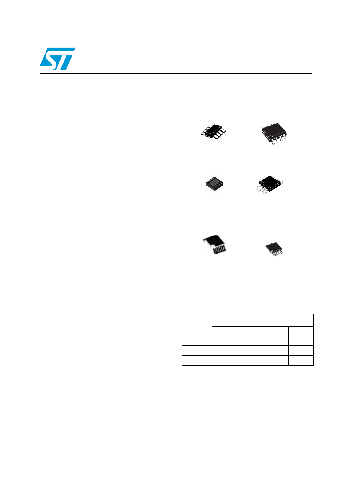
SOT23-8
DFN8 2x2
SO-8
MiniSO-8
Applications
■ Battery-powered applications
■ Portable devices
■ Signal conditioning
■ Active filtering
■ Medical instrumentation
Description
The TSV63x series of dual and quad operational
amplifiers offers low voltage operation and rail-torail input and output.
This family features an excellent speed/power
consumption ratio, offering a 880 kHz gainbandwidth product while consuming only 60 µA at
5 V supply voltage. The devices also feature an
ultra-low input bias current and have a shutdown
mode (TSV633, TSV635).
These features make the TSV63x family ideal for
sensor interfaces, battery-supplied and portable
applications, as well as active filtering.
TSSOP-14
Table 1. Device summary
Dual version Quad version
Reference
TSV63x
TSV63xA
Without
standby
TSV632 TSV633 TSV634 TSV635
TSV632A TSV633A TSV634A TSV635A
With
standby
TSSOP-16
Without
standby
With
standby
November 2011 Doc ID 15688 Rev 4 1/28
www.st.com
28

Contents TSV63x, TSV63xA
Contents
1 Package pin connections . . . . . . . . . . . . . . . . . . . . . . . . . . . . . . . . . . . . . 3
2 Absolute maximum ratings and operating conditions . . . . . . . . . . . . . 4
3 Electrical characteristics . . . . . . . . . . . . . . . . . . . . . . . . . . . . . . . . . . . . . 5
4 Application information . . . . . . . . . . . . . . . . . . . . . . . . . . . . . . . . . . . . . 13
4.1 Operating voltages . . . . . . . . . . . . . . . . . . . . . . . . . . . . . . . . . . . . . . . . . . 13
4.2 Rail-to-rail input . . . . . . . . . . . . . . . . . . . . . . . . . . . . . . . . . . . . . . . . . . . . 13
4.3 Rail-to-rail output . . . . . . . . . . . . . . . . . . . . . . . . . . . . . . . . . . . . . . . . . . . 13
4.4 Shutdown function (TSV633 - TSV635) . . . . . . . . . . . . . . . . . . . . . . . . . . 13
4.5 Optimization of DC and AC parameters . . . . . . . . . . . . . . . . . . . . . . . . . . 15
4.6 Driving resistive and capacitive loads . . . . . . . . . . . . . . . . . . . . . . . . . . . 15
4.7 PCB layouts . . . . . . . . . . . . . . . . . . . . . . . . . . . . . . . . . . . . . . . . . . . . . . . 15
4.8 Macromodel . . . . . . . . . . . . . . . . . . . . . . . . . . . . . . . . . . . . . . . . . . . . . . . 16
5 Package information . . . . . . . . . . . . . . . . . . . . . . . . . . . . . . . . . . . . . . . . 17
5.1 DFN8 2x2 package information . . . . . . . . . . . . . . . . . . . . . . . . . . . . . . . . 18
5.2 SOT23-8 package information . . . . . . . . . . . . . . . . . . . . . . . . . . . . . . . . . 20
5.3 SO-8 package information . . . . . . . . . . . . . . . . . . . . . . . . . . . . . . . . . . . . 21
5.4 MiniSO-8 package information . . . . . . . . . . . . . . . . . . . . . . . . . . . . . . . . . 22
5.5 MiniSO-10 package information . . . . . . . . . . . . . . . . . . . . . . . . . . . . . . . . 23
5.6 TSSOP14 package information . . . . . . . . . . . . . . . . . . . . . . . . . . . . . . . . 24
5.7 TSSOP16 package information . . . . . . . . . . . . . . . . . . . . . . . . . . . . . . . . 25
6 Ordering information . . . . . . . . . . . . . . . . . . . . . . . . . . . . . . . . . . . . . . . 26
7 Revision history . . . . . . . . . . . . . . . . . . . . . . . . . . . . . . . . . . . . . . . . . . . 27
2/28 Doc ID 15688 Rev 4
TSV63x, TSV63xA Package pin connections
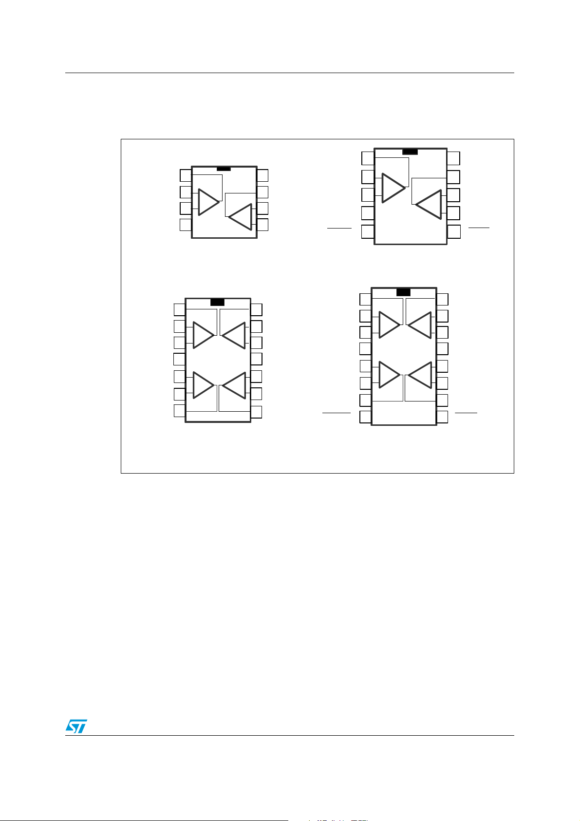
1 Package pin connections
Figure 1. Pin connections for each package (top view)
Out1
Out1
Out1
Out1
In1-
In1-
In1+
In1+
V
V
CC-
CC-
1
1
1
1
_
_
2
2
+
+
3
3
4
4
8
8
V
V
CC+
CC+
7
7
Out2
Out2
_
_
+
+
In2-
In2-
6
6
In2+
In2+
5
5
In1-
In1-
In1+
In1+
V
V
CC-
CC-
SHDN1
SHDN1SHDN1
_
_
2
2
+
+
3
3
4
4
5 6
5 6
10
10
V
V
CC+
CC+
9
9
Out2
Out2
_
_
+
+
8
8
7
7
In2-
In2-
In2+
In2+
SHDN2
SHDN2
SHDN2
TSV632IDT/IST/ILT/IQ2T
SO8/Mini-SO8/SOT23-8/DFN8
Out1
Out1
In1-
In1-
In1+
In1+
V
V
CC+
CC+
In2+
In2+
In2-
In2-
Out2
Out2
1
1
_
_
2
2
+
+
3
3
4
4
5
5
+
+
_
_
6
6
7
7
14
14
_
_
13
13
+
+
12
12
11
11
10
10
+
+
_
_
9
9
8
8
TSV634IPT
TSSOP14
Out4
Out4
In4-
In4-
In4+
In4+
V
V
CC-
CC-
In3+
In3+
In3-
In3-
Out3
Out3
Out1
In1-
In1+
V
CC+
In2+
In2-
Out2
SHDN1/2
SHDN1/2
TSV633IST
MiniSO-10
1
_
2
+
3
5
+
_
6
7 10
8 9
16
_
15
+
14
134
12
+
_
11
TSV635IPT
TSSOP16
Out4
In4-
In4+
V
CC-
In3+
In3-
Out3
SHDN3/4SHDN3/4
Doc ID 15688 Rev 4 3/28
Absolute maximum ratings and operating conditions TSV63x, TSV63xA
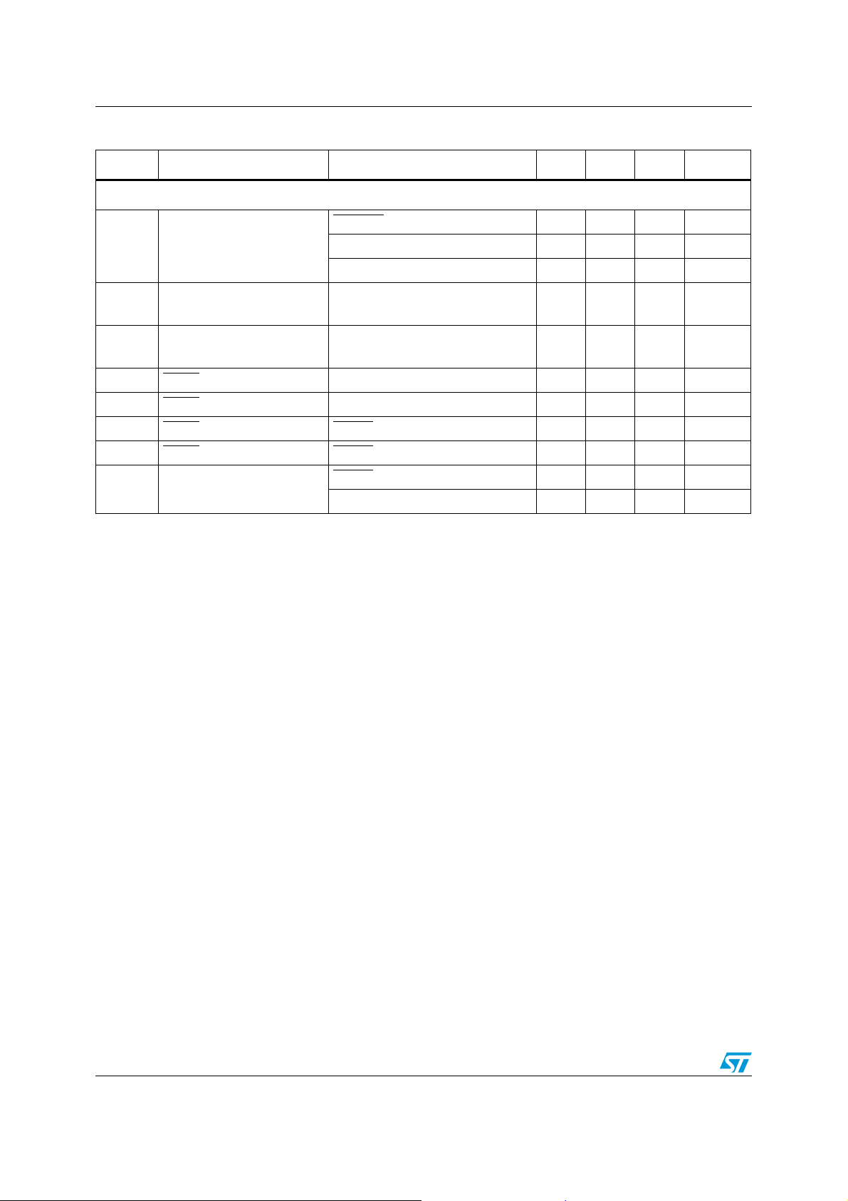
2 Absolute maximum ratings and operating conditions
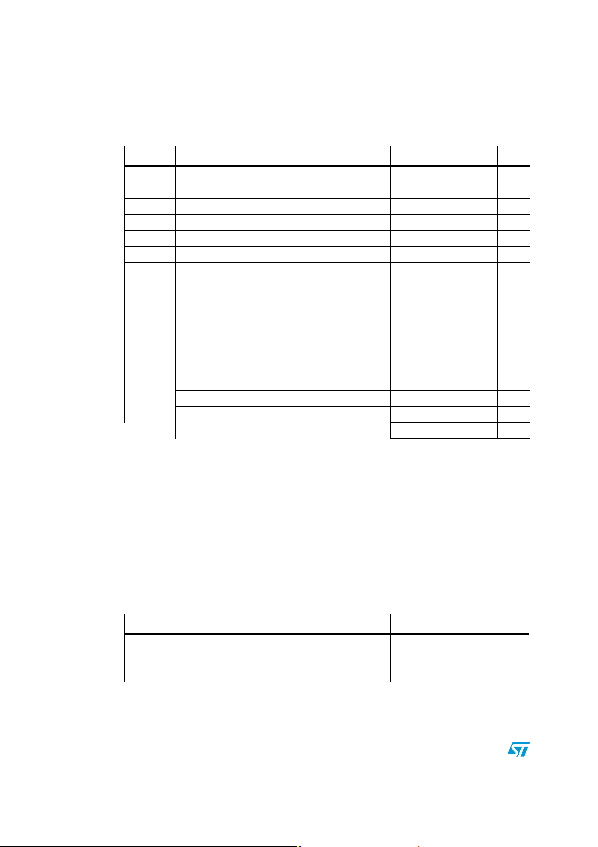
Table 2. Absolute maximum ratings (AMR)
Symbol Parameter Value Unit
(3)
(4)
(1)
(3)
(8)
(2)
(7)
(9)
(5)(6)
V
V
CC-
CC-
6V
±V
CC
- 0.2 to V
+ 0.2 V
CC+
V
10 mA
- 0.2 to V
+ 0.2 V
CC+
57
105
190
125
°C/W
113
100
95
4kV
300 V
1.5 kV
V
CC
V
V
I
in
Supply voltage
Differential input voltage
id
Input voltage
in
Input current
SHDN Shutdown voltage
T
stg
Storage temperature -65 to +150 °C
Thermal resistance junction to ambient
DFN8 2x2
SOT23-8
R
thja
MiniSO-8
SO-8
MiniSO-10
TSSOP14
TSSOP16
T
Maximum junction temperature 150 °C
j
HBM: human body model
ESD
MM: machine model
CDM: charged device model
Latch-up immunity 200 mA
1. All voltage values, except differential voltage are with respect to network ground terminal.
2. Differential voltages are the non-inverting input terminal with respect to the inverting input terminal.
3. VCC-Vin must not exceed 6 V, Vin must not exceed 6V.
4. Input current must be limited by a resistor in series with the inputs.
5. Short-circuits can cause excessive heating and destructive dissipation.
are typical values.
6. R
th
7. Human body model: 100 pF discharged through a 1.5 kΩ resistor between two pins of the device, done for
all couples of pin combinations with other pins floating.
8. Machine model: a 200 pF cap is charged to the specified voltage, then discharged directly between two
pins of the device with no external series resistor (internal resistor < 5 Ω), done for all couples of pin
combinations with other pins floating.
9. Charged device model: all pins plus package are charged together to the specified voltage and then
discharged directly to the ground.
Table 3. Operating conditions
Symbol Parameter Value Unit
T
V
V
CC
icm
oper
Supply voltage 1.5 to 5.5 V
Common mode input voltage range V
CC-
- 0.1 to V
+ 0.1 V
CC+
Operating free air temperature range -40 to +125 °C
4/28 Doc ID 15688 Rev 4
TSV63x, TSV63xA Electrical characteristics
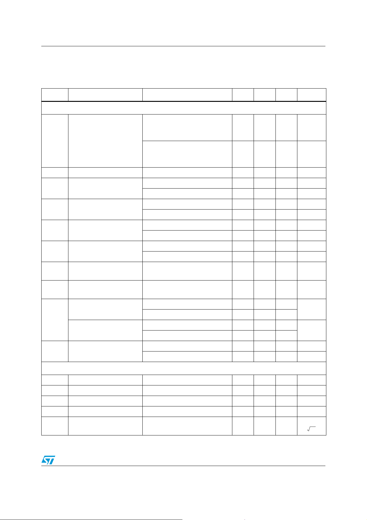
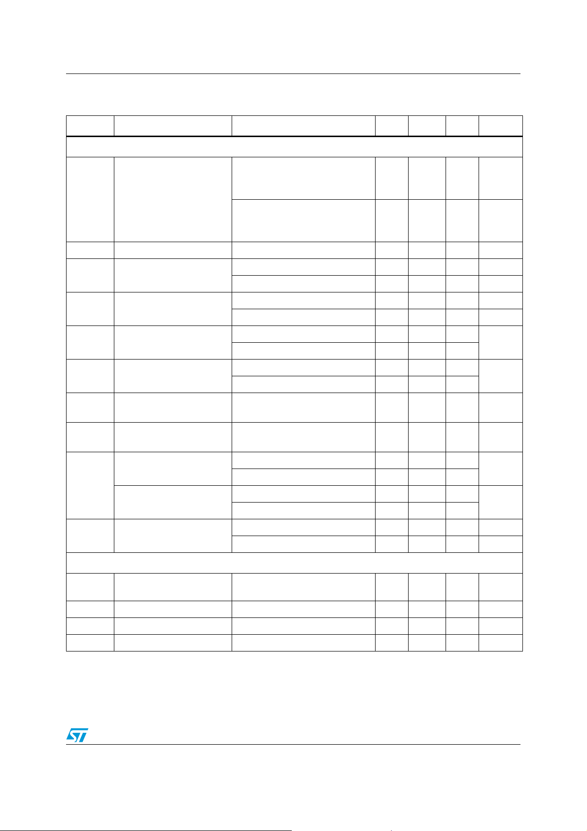
3 Electrical characteristics
Table 4. Electrical characteristics at V
Symbol Parameter Conditions Min. Typ. Max. Unit
DC performance
and R
= +1.8 V with V
connected to VCC/2 (unless otherwise specified)
L
CC+
= 0 V, V
CC-
= VCC/2, T
icm
= 25° C,
amb
V
DV
CMR
A
V
V
I
I
Offset voltage
io
Input offset voltage drift 2 μV/°C
io
I
Input offset current
io
I
Input bias current
ib
Common mode rejection
ratio 20 log (ΔV
Large signal voltage gain
vd
High level output voltage
OH
Low level output voltage
OL
I
sink
out
I
source
Supply current (per
CC
operator)
AC performance
/ΔVio)
ic
TSV63x
TSV63xA
TSV633AIST - MiniSO10
< Top < T
T
min
T
< Top < T
min
< Top < T
T
min
(V
out=VCC
T
min
(V
out=VCC
T
min
/2) 1 10
< Top < T
/2) 1 10
< Top < T
0 V to 1.8 V, V
T
< Top < T
min
R
= 10 kΩ, V
L
< Top < T
T
min
=10kΩ
R
L
< Top < T
T
min
=10kΩ
R
L
< Top < T
T
min
TSV63x
max -
- TSV63xA
max
- TSV633AIST
max
1 100 pA
max
max
= 0.9 V 53 74 dB
out
max
= 0.5 V to 1.3 V 85 95 dB
out
max
51 dB
80 dB
35
max
max
50
Vo = 1.8 V 6 12
T
min
< Top < T
max
4
Vo = 0 V 6 10
< Top < T
T
min
No load, V
< Top < T
T
min
max
out=VCC
max
/2 40 50 60 µA
4
3
0.8
mV
1
4.5
2
mV
2.2
(1)
(1)
pA
pA
1 100 pA
5
435
50
mV
mV
mA
mA
62 µA
GBP Gain bandwidth product R
φm Phase margin R
G
Gain margin RL=2kΩ, CL= 100 pF 13 dB
m
SR Slew rate R
Equivalent input noise
e
n
voltage
1. Guaranteed by design.
=2kΩ, CL= 100 pF, f = 100 kHz 700 790 kHz
L
=2kΩ, CL= 100 pF 45 Degrees
L
=2kΩ, CL= 100 pF, Av = 1 0.2 0.27 V/μs
L
f = 1 kHz
f = 10 kHz
60
33
Doc ID 15688 Rev 4 5/28
nV
-----------Hz
Electrical characteristics TSV63x, TSV63xA
Table 5. Shutdown characteristics VCC=1.8V
Symbol Parameter Conditions Min. Typ. Max. Unit
DC performance
I
CC
t
on
t
off
V
IH
V
I
IH
I
IL
I
OLeak
V
CC-
< Top < 85° C 200 nA
min
< Top < 125° C 1.5 µA
min
= V
out
out
= V
CC-
CC+
to V
+0.2 V
CC-
- 0.5 V to V
CC+
- 0.7 V
Supply current in shutdown
mode (all operators)
Amplifier turn-on time
Amplifier turn-off time
SHDN =
T
T
RL= 2 kΩ,
V
RL=2kΩ,
V
SHDN logic high 1.35 V
SHDN logic low 0.6 V
IL
SHDN current high SHDN = V
SHDN current low SHDN = V
Output leakage in shutdown
mode
SHDN
T
min
CC+
CC-
= V
CC-
< Top < 125° C 1 nA
2.5 50 nA
200 ns
20 ns
10 pA
10 pA
50 pA
6/28 Doc ID 15688 Rev 4
TSV63x, TSV63xA Electrical characteristics
Table 6. V
CC+
= +3.3 V, V
= 0 V, V
CC-
= VCC/2, T
icm
= 25° C, RL connected to VCC/2
amb
(unless otherwise specified)
Symbol Parameter Conditions Min. Typ. Max. Unit
DC performance
V
DV
I
I
CMR
A
V
V
I
out
I
CC
Offset voltage
io
Input offset voltage drift 2 μV/°C
io
Input offset current
io
Input bias current
ib
Common mode rejection
ratio 20 log (ΔVic/ΔVio)
Large signal voltage gain
vd
High level output voltage
OH
Low level output voltage
OL
I
sink
I
source
Supply current (per
operator)
AC performance
TSV63x
TSV63xA
TSV633AIST - MiniSO10
T
< Top < T
min
< Top < T
T
min
< Top < T
T
min
V
out=VCC
T
min
V
out=VCC
T
min
/2 1 10
< Top < T
/2 1 10
< Top < T
0V to 3.3V, V
< Top < T
T
min
RL=10kΩ, V
< Top < T
T
min
=10kΩ
R
L
T
< Top < T
mi.
=10kΩ
R
L
T
< Top < T
min
TSV63x
max -
- TSV63xA
max
- TSV633AIST
max
max
max
= 1.65 V 57 79
out
max
= 0.5 V to 2.8 V 88 98
out
max
53
83
35
max
max
50
Vo = 3.3 V 23 45
T
min
< Top < T
max
20
Vo = 0 V 23 38
< Top < T
T
min
No load, V
< Top < T
T
min
max
= 1.75 V 43 55 64 µA
out
max
20
1 100 pA
1 100 pA
5
435
3
0.8
1
4.5
2
2.2
(1)
(1)
50
66 µA
mV
mV
pA
pA
dB
dB
mV
mV
mA
mA
GBP Gain bandwidth product
φm Phase margin R
G
Gain margin RL = 2 kΩ, CL= 100 pF 13 dB
m
SR Slew rate R
1. Guaranteed by design.
RL=2kΩ, CL= 100 pF,
f = 100 kHz
= 2 kΩ, CL= 100 pF 46 Degrees
L
=2kΩ, CL= 100 pF, AV= 1 0.22 0.29 V/μs
L
710 860 kHz
Doc ID 15688 Rev 4 7/28
Electrical characteristics TSV63x, TSV63xA
Table 7. Electrical characteristics at V
and R
= +5 V with V
connected to VCC/2 (unless otherwise specified)
L
CC+
= 0 V, V
CC-
= VCC/2, T
icm
= 25° C,
amb
Symbol Parameter Conditions Min. Typ. Max. Unit
DC performance
V
io
DV
io
I
io
I
ib
CMR
SVR
A
vd
EMIRR
V
OH
V
OL
TSV63x
TSV63xA
TSV633AIST - MiniSO10
Offset voltages
T
min
T
min
T
min
< Top < T
< Top < T
< Top < T
TSV63x
max -
- TSV63xA
max
- TSV633AIST
max
Input offset voltage drift 2 μV/°C
Input offset current
Input bias current
Common mode rejection
ratio 20 log (ΔVic/ΔVio)
Supply voltage rejection
ratio 20 log (ΔV
CC
/ΔVio)
Large signal voltage gain
EMI rejection ratio
EMIRR = -20 log (V
RFpeak
/ΔVio)
High level output voltage
Low level output voltage
(V
out=VCC
T
min
(V
out=VCC
T
min
0 V to 5 V, V
T
min
V
CC
T
min
R
= 10 kΩ, V
L
T
min
V
RF
V
RF
V
RF
V
RF
=10kΩ
R
L
T
min
=10kΩ
R
L
T
min
/2) 1 10
< Top < T
max
1 100 pA
/2) 1 10
< Top < T
< Top < T
max
= 2.5 V 60 80 dB
out
max
55 dB
1 100 pA
= 1.8 to 5 V 75 102
< Top < T
< Top < T
= 100 mV
= 100 mV
= 100 mV
= 100 mV
< Top < T
max
= 0.5 V to 4.5 V 89 98 dB
out
max
f = 400 MHz 61
rms,
f = 900 MHz 85
rms,
, f =1800 MHz 92
rms
, f =2400 MHz 83
rms
max
73
84 dB
35
7
50
635
< Top < T
max
3
0.8
1
4.5
2
2.2
(1)
(1)
50
Vo = 5 V 40 69
I
sink
I
out
I
source
I
CC
Supply current (per
operator)
T
min
< Top < T
max
35
Vo = 0 V 40 74
< Top < T
T
min
No load, V
< Top < T
T
min
max
out=VCC
max
/2 50 60 69 µA
35
72 µA
AC performance
mV
mV
pA
pA
dB
dB
mV
mV
mA
mA
GBP Gain bandwidth product RL=2kΩ, CL= 100 pF, f = 100 kHz 730 880 kHz
F
Unity gain frequency RL=2kΩ, CL= 100 pF, 830 kHz
u
8/28 Doc ID 15688 Rev 4
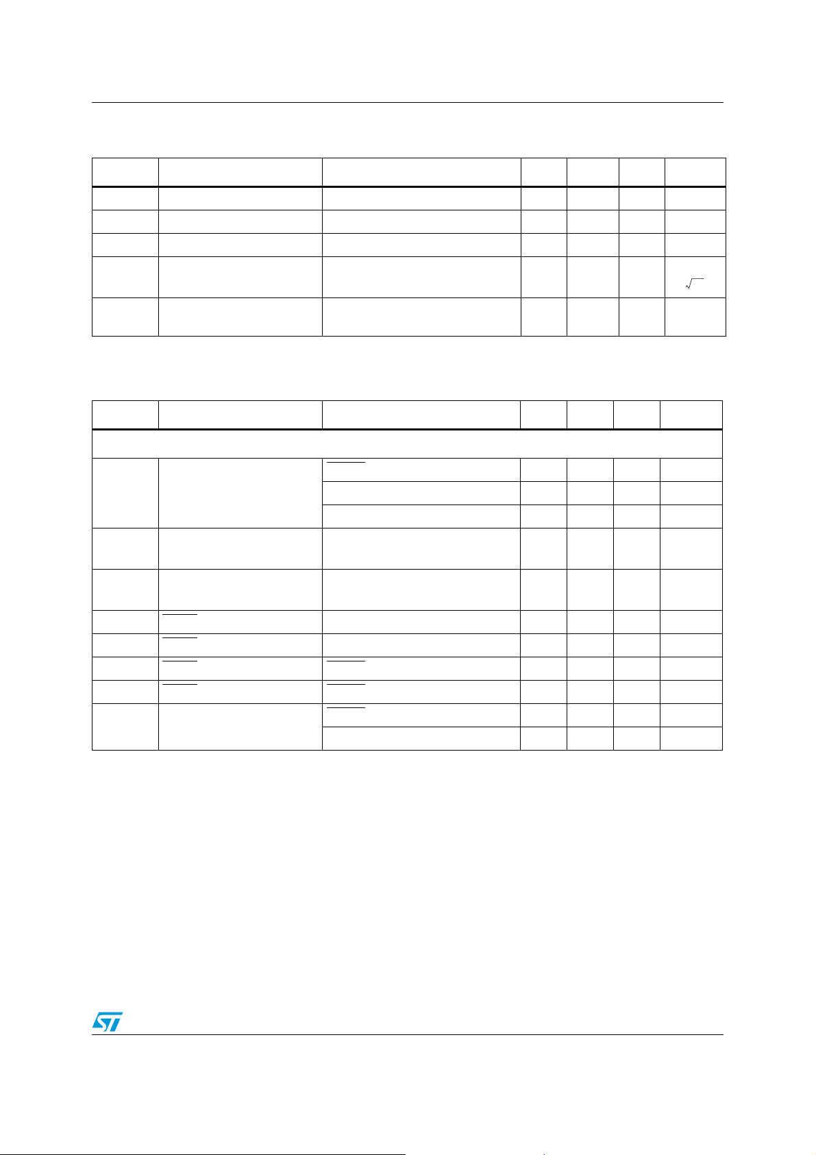
TSV63x, TSV63xA Electrical characteristics
Table 7. Electrical characteristics at V
and R
connected to VCC/2 (unless otherwise specified) (continued)
L
= +5 V with V
CC+
= 0 V, V
CC-
= VCC/2, T
icm
= 25° C,
amb
Symbol Parameter Conditions Min. Typ. Max. Unit
φm Phase margin RL=2kΩ, CL= 100 pF 48 Degrees
G
SR Slew rate R
e
THD+e
1. Guaranteed by design.
Table 8. Shutdown characteristics at VCC= 5 V
Gain margin RL=2kΩ, CL= 100 pF 13 dB
m
=2kΩ, CL= 100 pF, Av=1 0.25 0.34 V/μs
L
Equivalent input noise
n
voltage
Total harmonic distortion +
n
noise
f=1kHz
f = 10 kHz
VCC = 5V, f = 1kHz, AV = 1, RL =
100kΩ, V
= VCC/2, V
icm
out
= 2V
PP
60
33
0.002 %
Symbol Parameter Conditions Min. Typ. Max. Unit
DC performance
I
CC
t
on
t
off
V
V
I
IH
I
IL
I
OLeak
SHDN = V
Supply current in shutdown
mode (all operators)
Amplifier turn-on time
Amplifier turn-off time
SHDN logic high 2 V
IH
SHDN logic low 0.8 V
IL
T
min
T
min
RL = 2 kΩ,
V
out
RL = 2 kΩ,
V
out
SHDN current high SHDN = V
SHDN current low SHDN = V
Output leakage in shutdown
mode
SHDN
T
min
CC-
< Top < 85° C 200 nA
< Top < 125° C 1.5 µA
= V
= V
CC-
CC+
= V
CC+
CC-
CC-
V to V
CC-
- 0.5 V to V
+0.2 V
CC+
- 0.7 V
< Top < 125° C 1 nA
550 nA
200 ns
20 ns
10 pA
10 pA
50 pA
nV
-----------Hz
Doc ID 15688 Rev 4 9/28
 Loading...