

ST TSV6292, TSV6293, TSV6294, TSV6295, TSV6292A User Manual
...
Micropower, wide bandwidth CMOS operational amplifiers
Features
■ Rail-to-rail input and output
■ Low power consumption: 29 µA typ, 36 µA max
■ Low supply voltage: 1.5 – 5.5 V
■ High gain bandwidth product: 1.3 MHz typ
■ Stable when used in gain configuration
■ Low power shutdown mode: 5 nA typ
■ Good accuracy: 800 µV max (A version)
■ Low input bias current: 1 pA typ
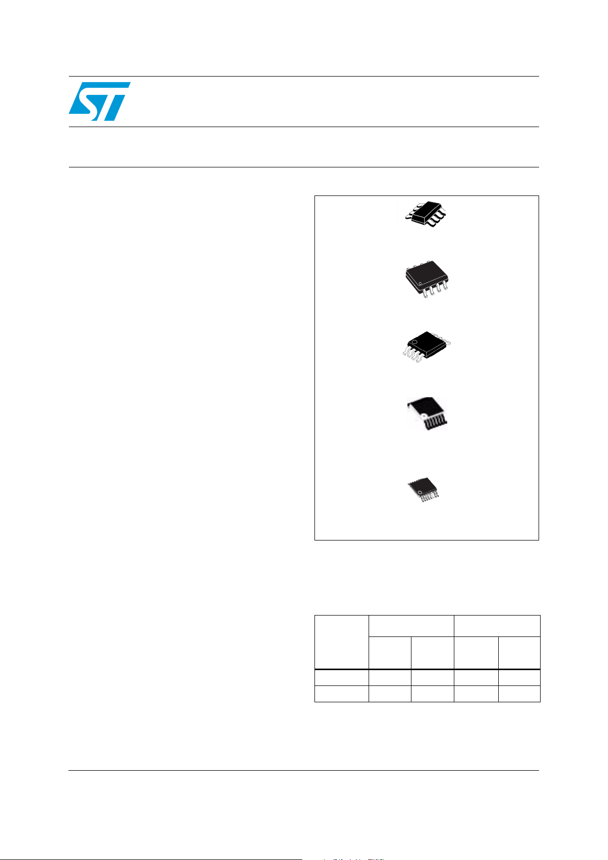
■ Micropackages: MiniSO-8, SOT23-8,
MiniSO-10, TSSOP14, TSSOP16
■ EMI hardened operational amplifiers
■ High tolerance to ESD: 4 kV HBM
■ Extended temperature range: -40 to +125° C
TSV629x, TSV629xA
SOT23-8
SO-8
MiniSO-8/10
Applications
■ Battery-powered applications
■ Portable devices
■ Signal conditioning
■ Active filtering
■ Medical instrumentation
Description
The TSV6292, TSV6293, TSV6294 and TSV6295
dual and quad operational amplifiers offer a high
bandwidth of 1.3 MHz while consuming only
29 µA. They must be used in a gain configuration
(equal or above +4 or -3).
The TSV629x series features low voltage, low
power operation and rail-to-rail input and output.
The devices also offer an ultra-low input bias
current and low input offset voltage.
The TSV6293 (dual) and TSV6295 (quad) have
two shutdown pins for reduced power
consumption.
TSSOP-14
TSSOP-16
These features make the TSV629x family ideal
for sensor interfaces, battery supplied and
portable applications, as well as active filtering.
Table 1. Device summary
Dual version Quad version
Reference
TSV629x
TSV629xA
Without
standby
TSV6292 TSV6293 TSV6294 TSV6295
TSV6292A TSV6293A TSV6294A TSV6295A
With
standby
Without
standby
With
standby
March 2010 Doc ID 16882 Rev 2 1/25
www.st.com
25

Contents TSV629x, TSV629xA
Contents
1 Package pin connections . . . . . . . . . . . . . . . . . . . . . . . . . . . . . . . . . . . . . 3
2 Absolute maximum ratings and operating conditions . . . . . . . . . . . . . 4
3 Electrical characteristics . . . . . . . . . . . . . . . . . . . . . . . . . . . . . . . . . . . . . 5
4 Application information . . . . . . . . . . . . . . . . . . . . . . . . . . . . . . . . . . . . . 13
4.1 Operating voltages . . . . . . . . . . . . . . . . . . . . . . . . . . . . . . . . . . . . . . . . . . 13
4.2 Rail-to-rail input . . . . . . . . . . . . . . . . . . . . . . . . . . . . . . . . . . . . . . . . . . . . 13
4.3 Rail-to-rail output . . . . . . . . . . . . . . . . . . . . . . . . . . . . . . . . . . . . . . . . . . . 13
4.4 Optimization of DC and AC parameters . . . . . . . . . . . . . . . . . . . . . . . . . . 14
4.5 Shutdown function (TSV6293, TSV6295) . . . . . . . . . . . . . . . . . . . . . . . . 14
4.6 Driving resistive and capacitive loads . . . . . . . . . . . . . . . . . . . . . . . . . . . 15
4.7 PCB layouts . . . . . . . . . . . . . . . . . . . . . . . . . . . . . . . . . . . . . . . . . . . . . . . 15
4.8 Macromodel . . . . . . . . . . . . . . . . . . . . . . . . . . . . . . . . . . . . . . . . . . . . . . . 15
5 Package information . . . . . . . . . . . . . . . . . . . . . . . . . . . . . . . . . . . . . . . . 16
5.1 SOT23-8 package information . . . . . . . . . . . . . . . . . . . . . . . . . . . . . . . . . 17
5.2 SO-8 package information . . . . . . . . . . . . . . . . . . . . . . . . . . . . . . . . . . . . 18
5.3 MiniSO-8 package information . . . . . . . . . . . . . . . . . . . . . . . . . . . . . . . . . 19
5.4 MiniSO-10 package information . . . . . . . . . . . . . . . . . . . . . . . . . . . . . . . . 20
5.5 TSSOP14 package information . . . . . . . . . . . . . . . . . . . . . . . . . . . . . . . . 21
5.6 TSSOP16 package information . . . . . . . . . . . . . . . . . . . . . . . . . . . . . . . . 22
6 Ordering information . . . . . . . . . . . . . . . . . . . . . . . . . . . . . . . . . . . . . . . 23
7 Revision history . . . . . . . . . . . . . . . . . . . . . . . . . . . . . . . . . . . . . . . . . . . 24
2/25 Doc ID 16882 Rev 2
TSV629x, TSV629xA Package pin connections
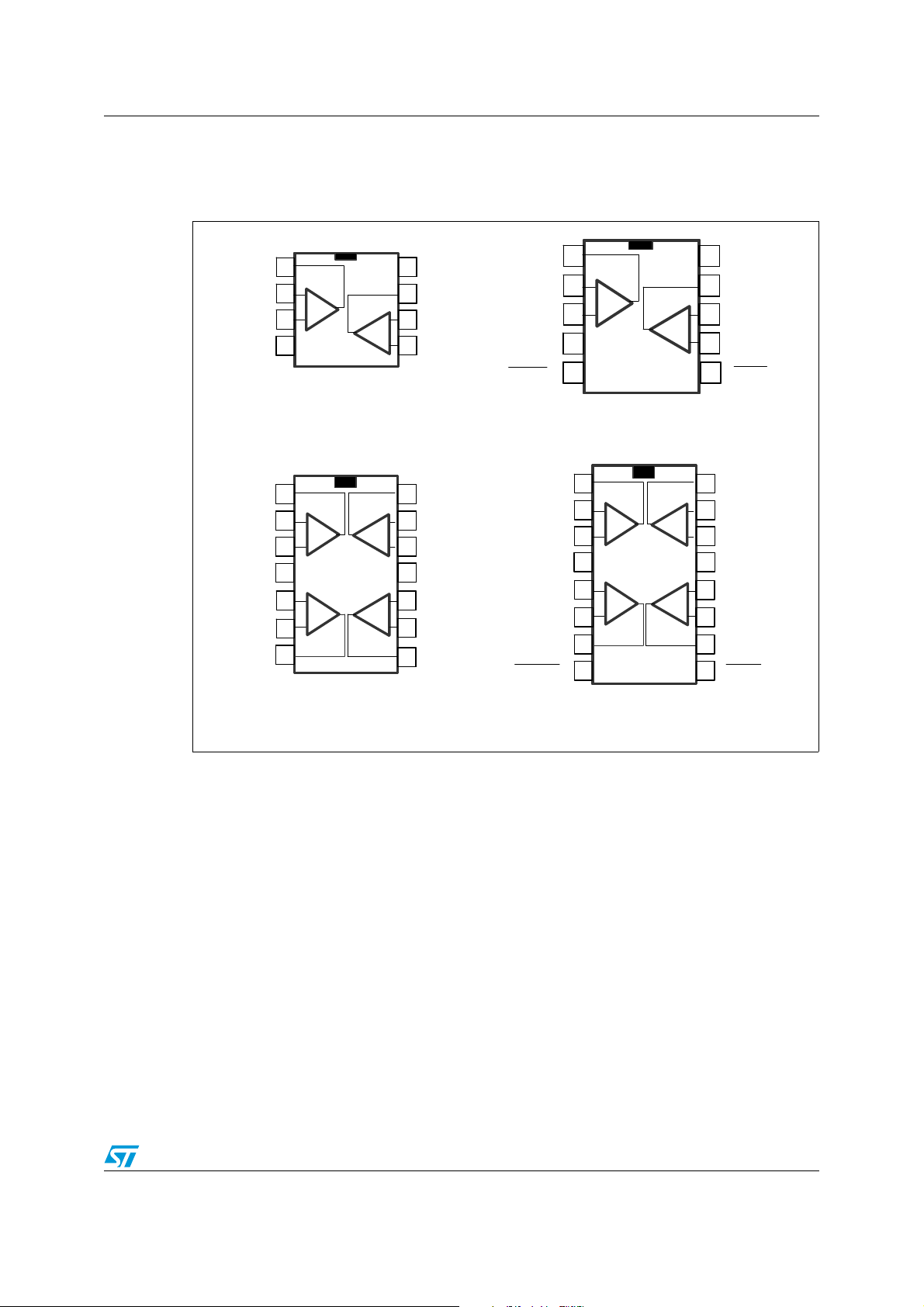
1 Package pin connections
Figure 1. Pin connections for each package (top view)
Out1
Out1
Out1
Out1
1
1
_
In1-
In1-
In1+
In1+
V
V
CC-
CC-
_
2
2
+
+
3
3
4
4
TSV6292IDT/IST/ILT
SO8/Mini-SO8/SOT23-8
1
8
8
V
V
CC+
CC+
7
7
Out2
Out2
_
_
+
+
In2-
In2-
6
6
In2+
In2+
5
5
SHDN1
SHDN1SHDN1
1
_
In1-
In1-
In1+
In1+
V
V
CC-
CC-
_
2
2
+
+
3
3
4
4
5 6
5 6
TSV6293IST
MiniSO-10
10
10
V
V
CC+
CC+
9
9
Out2
Out2
_
_
+
+
8
8
7
7
In2-
In2-
In2+
In2+
SHDN2
SHDN2
SHDN2
Out1
Out1
In1-
In1-
In1+
In1+
V
V
CC+
CC+
In2+
In2+
In2-
In2-
Out2
Out2
1
1
_
_
2
2
+
+
3
3
4
4
5
5
+
+
_
_
6
6
7
7
TSV6294IPT
TSSOP14
1
Out4
Out4
14
14
_
_
13
13
In4-
In4-
+
+
In4+
In4+
12
12
V
V
11
11
CC-
CC-
10
10
In3+
In3+
+
+
_
_
In3-
In3-
9
9
Out3
Out3
8
8
Out1
In1-
In1+
V
CC+
In2+
In2-
Out2
SHDN1/2
SHDN1/2
_
2
+
3
5
+
_
6
7 10
8 9
_
+
Out4
16
15
In4-
In4+
14
V
134
CC-
12
In3+
+
_
In3-
11
Out3
SHDN3/4SHDN3/4
TSV6295IPT
TSSOP16
Doc ID 16882 Rev 2 3/25
Absolute maximum ratings and operating conditions TSV629x, TSV629xA
2 Absolute maximum ratings and operating conditions
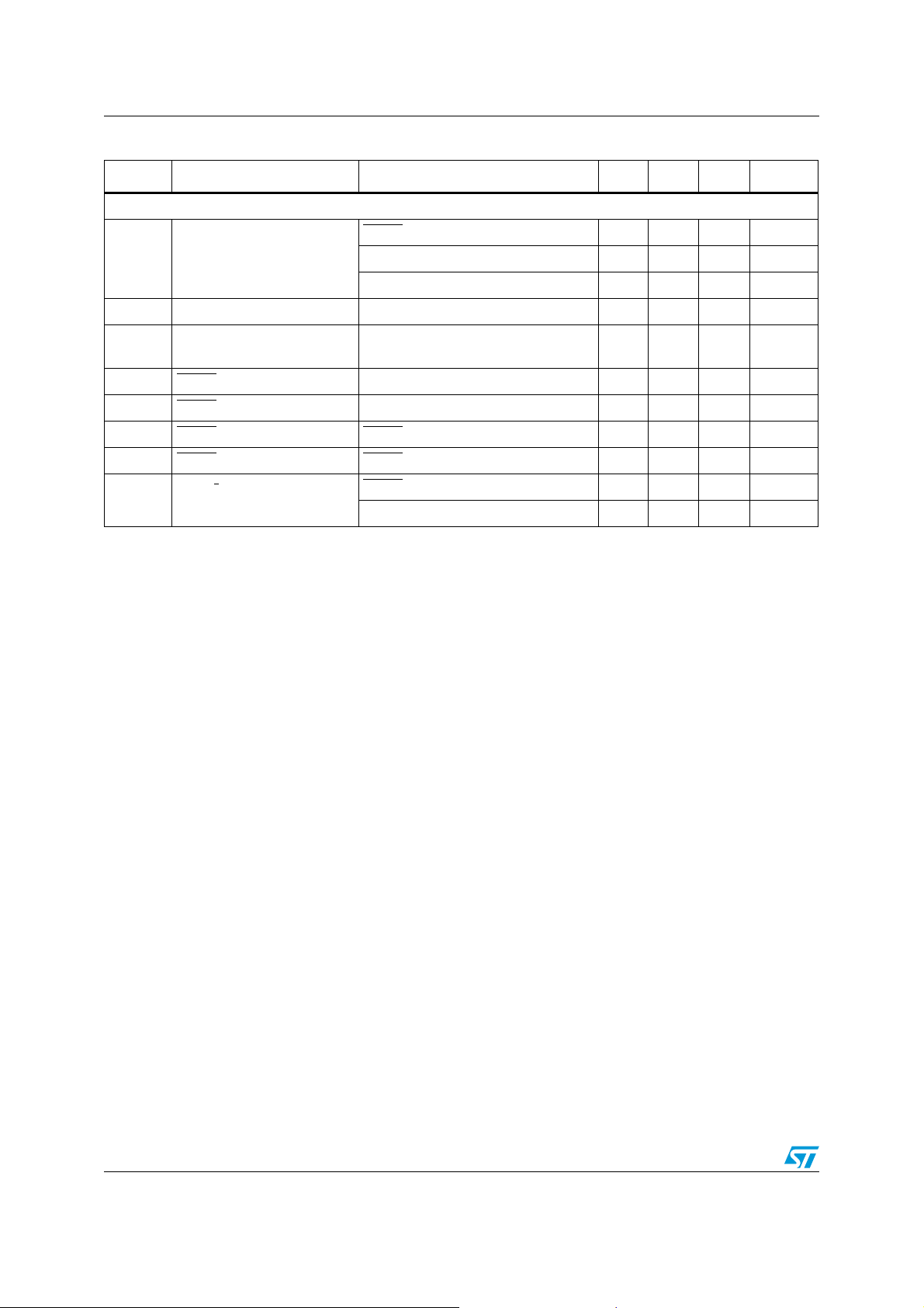
Table 2. Absolute maximum ratings (AMR)
Symbol Parameter Value Unit
(3)
(4)
(1)
(3)
(8)
(2)
(7)
(9)
(5)(6)
V
V
CC-
CC-
6V
±V
CC
- 0.2 to V
+ 0.2 V
CC+
V
10 mA
- 0.2 to V
+ 0.2 V
CC+
105
190
125
°C/W
113
100
95
4kV
200 V
1.5 kV
V
CC
V
V
I
in
Supply voltage
Differential input voltage
id
Input voltage
in
Input current
SHDN Shutdown voltage
T
stg
Storage temperature -65 to +150 °C
Thermal resistance junction to ambient
SOT23-8
MiniSO-8
R
thja
SO-8
Mini-SO10
TSSOP14
TSSOP16
T
Maximum junction temperature 150 °C
j
HBM: human body model
ESD
MM: machine model
CDM: charged device model
Latch-up immunity 200 mA
1. All voltage values, except differential voltages are with respect to network ground terminal.
2. Differential voltages are the non-inverting input terminal with respect to the inverting input terminal.
3. VCC-Vin must not exceed 6 V, Vin must not exceed 6V.
4. Input current must be limited by a resistor in series with the inputs.
5. Short-circuits can cause excessive heating and destructive dissipation.
6. Rth are typical values.
7. Human body model: 100 pF discharged through a 1.5 kΩ resistor between two pins of the device, done for
all couples of pin combinations with other pins floating.
8. Machine model: a 200 pF capacitor is charged to the specified voltage, then discharged directly between
two pins of the device with no external series resistor (internal resistor < 5 Ω), done for all couples of pin
combinations with other pins floating.
9. Charged device model: all pins plus package are charged together to the specified voltage and then
discharged directly to ground.
Table 3. Operating conditions
Symbol Parameter Value Unit
T
V
V
CC
icm
oper
Supply voltage 1.5 to 5.5 V
Common mode input voltage range V
- 0.1 to V
CC-
+ 0.1 V
CC+
Operating free air temperature range -40 to +125 °C
4/25 Doc ID 16882 Rev 2
TSV629x, TSV629xA Electrical characteristics
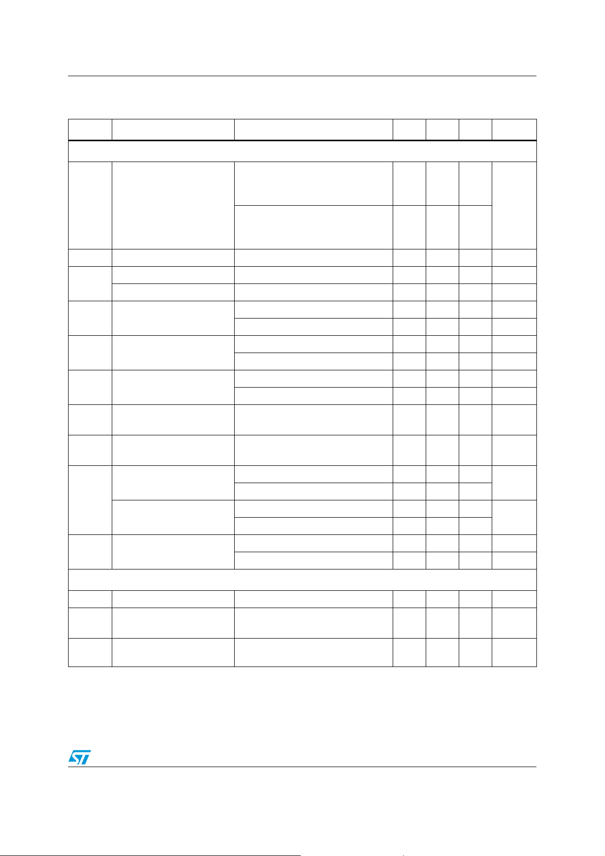
3 Electrical characteristics
Table 4. Electrical characteristics at V
Symbol Parameter Conditions Min. Typ. Max. Unit
DC performance
V
io
DV
io
I
io
I
ib
CMR
A
vd
V
OH
V
OL
I
out
I
CC
AC performance
GBP Gain bandwidth product R
Gain Minimum gain for stability
SR Slew rate
1. Guaranteed by design.
and R
connected to VCC/2 (unless otherwise specified)
L
TSV629x
TSV629xA
TSV6293AIST - MiniSO-10
= +1.8 V with V
CC+
= 0 V, V
CC-
= VCC/2, T
icm
amb
4
0.8
1
= 25° C,
mV
Offset voltage
TSV629x -T
TSV629xA - T
< Top < T
min
min
TSV6293AIST - T
max
< Top < T
< Top < T
min
max
max
6
2
2.2
Input offset voltage drift 2 μV/°C
Input offset current
(V
out=VCC
/2)
Input bias current
(V
out=VCC
/2)
Common mode rejection
ratio 20 log (ΔV
/ΔVio)
ic
Large signal voltage gain
High level output voltage
Low level output voltage
Isink
Isource
Supply current (per operator)
110
T
< Top < T
min
max
1100 pA
110
< Top < T
T
min
0 V to 1.8 V, V
< Top < T
T
min
R
= 10 kΩ, V
L
T
< Top < T
min
R
=10kΩ
L
T
< Top < T
min
R
=10kΩ
L
T
< Top < T
min
V
= 1.8 V 6 12
out
< Top < T
T
min
V
= 0 V 6 10
out
< Top < T
T
min
No load, V
T
< Top < T
min
=10kΩ, CL= 100 pF 1.1 MHz
L
max
= 0.9 V 53 74 dB
out
max
= 0.5 V to 1.3 V 78 95 dB
out
max
51 dB
73 dB
35
max
max
max
max
out=VCC
max
/2 25 31 µA
50
4
4
Phase margin = 60°, Rf = 10kΩ,
=10kΩ, CL=20pF, Top=25°C
R
L
RL=10kΩ, CL=100pF, V
= 0.5 V
out
to 1.3V
1100 pA
5
435
+4
-3
0.33 V/μs
(1)
(1)
50
33 µA
pA
pA
mV
mV
mA
V/V
Doc ID 16882 Rev 2 5/25
Electrical characteristics TSV629x, TSV629xA
Table 5. Shutdown characteristics VCC= 1.8 V (TSV6293, TSV6295)
Symbol Parameter Conditions Min. Typ. Max. Unit
DC performance
I
CC
t
on
t
off
V
V
I
IH
I
IL
I
OLeak
= V
SHDN
Supply current in shutdown
mode (all operators)
T
min
T
min
Amplifier turn-on time RL=5k, Vout=V
R
Amplifier turn-off time
SHDN logic high 1.35 V
IH
SHDN logic low 0.6 V
IL
V
L
CC+
SHDN current high SHDN =V
SHDN current low SHDN =V
Output leakage in shutdown
mode
SHDN
T
min
CC-
< Top < 85° C 200 nA
< Top < 125° C 1.5 µA
=5k, Vout=V
CC-
CC+
to V
- 0.5 V to
+ 0.2 V 200 ns
CC-
- 0.7 V
CC+
CC-
=V
CC-
< Top < 125° C 1 nA
2.5 50 nA
20 ns
10 pA
10 pA
50 pA
6/25 Doc ID 16882 Rev 2
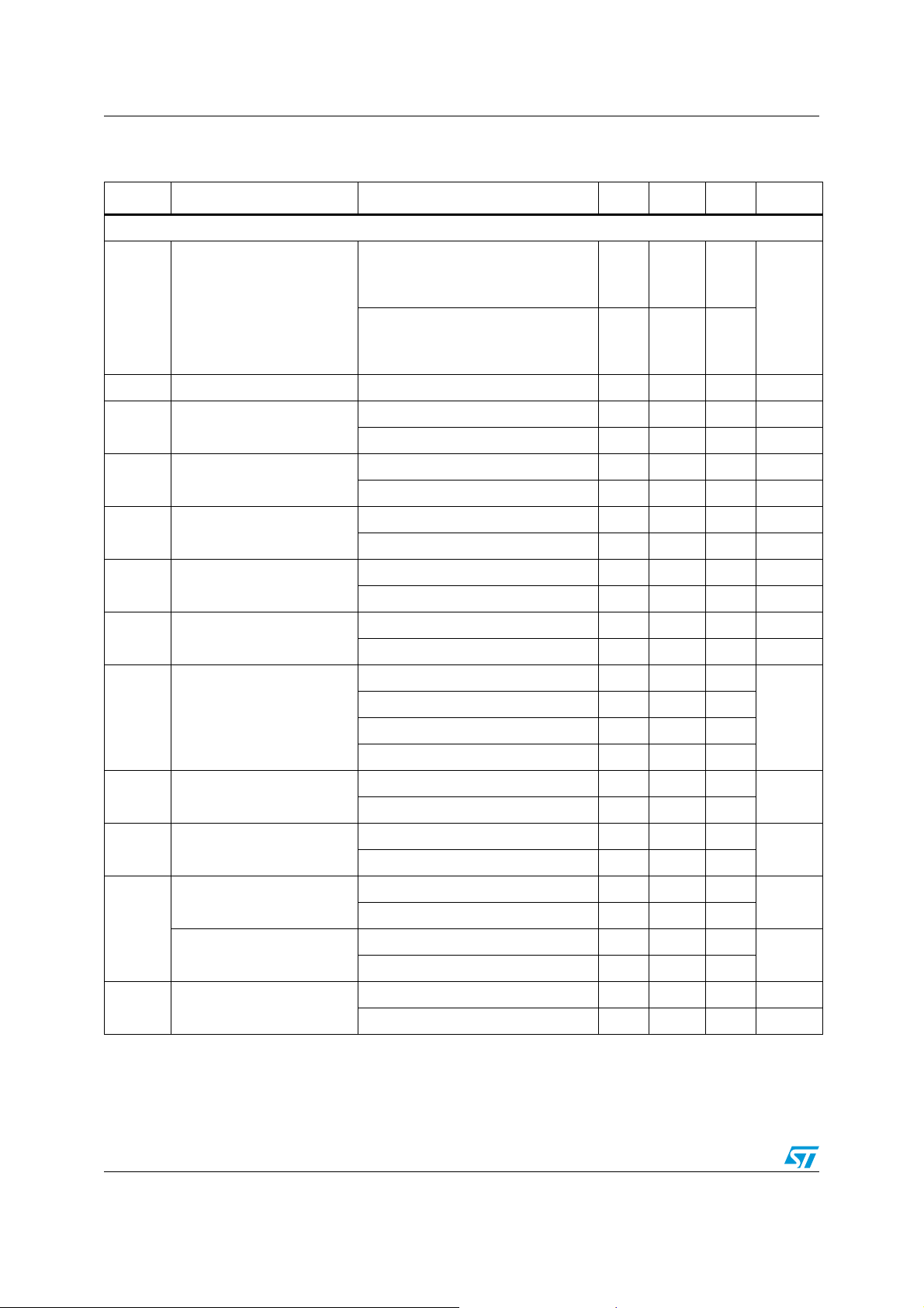
TSV629x, TSV629xA Electrical characteristics
Table 6. V
CC+
= +3.3 V, V
= 0 V, V
CC-
= VCC/2, T
icm
= 25° C, RL connected to VCC/2
amb
(unless otherwise specified)
Symbol Parameter Conditions Min. Typ. Max. Unit
DC performance
V
DV
Offset voltage
io
Input offset voltage drift 2 μV/°C
io
Input offset current 1 10
I
io
I
Input bias current
ib
CMR
A
V
V
Common mode rejection
ratio 20 log (ΔVic/ΔVio)
Large signal voltage gain
vd
High level output voltage
OH
Low level output voltage
OL
Isink
I
out
Isource
I
Supply current (per operator)
CC
AC performance
TSV629x
TSV629xA
TSV6293AIST - MiniSO-10
TSV629x -T
TSV629xA - T
TSV6293AIST - T
T
< Top < T
min
T
< Top < T
min
0 V to 3.3 V, V
< Top < T
T
min
RL=10 kΩ, V
< Top < T
T
min
=10kΩ
R
L
T
< Top < T
min
=10kΩ
R
L
T
< Top < T
min
V
= 5 V 23 45
o
< Top < T
T
min
V
= 0 V 23 38
o
< Top < T
T
min
No load, V
< Top < T
T
min
< Top < T
min
< Top < T
min
max
max
out
max
= 0.5 V to 2.8 V 81 98 dB
out
max
max
max
< Top < T
min
max
= 1.65 V 57 79 dB
53 dB
76 dB
35
max
max
max
max
=2.5V 26 33 µA
out
max
50
20
20
1 100 pA
110
1 100 pA
5
435
4
0.8
1
6
2
2.2
(1)
(1)
50
35 µA
mV
pA
pA
mV
mV
mA
mA
GBP Gain bandwidth product RL=10kΩ, CL= 100 pF 1.2 MHz
Gain Minimum gain for stability
SR Slew rate
1. Guaranteed by design.
Phase margin = 60°, Rf = 10kΩ,
=10kΩ, CL=20pF, Top=25°C
R
L
RL=10kΩ, CL=100pF, V
= 0.5 V
out
to 2.8 V
+4
-3
0.4 V/μs
Doc ID 16882 Rev 2 7/25
V/V
Electrical characteristics TSV629x, TSV629xA
Table 7. V
CC+
= +5 V, V
= 0 V, V
CC-
= VCC/2, T
icm
= 25° C, RL connected to VCC/2
amb
(unless otherwise specified)
Symbol Parameter Conditions Min. Typ. Max. Unit
DC performance
V
io
DV
io
I
io
I
ib
CMR
A
vd
SVR
EMIRR
V
OH
V
OL
I
out
I
CC
TSV629x
TSV629xA
TSV6293AIST - MiniSO-10
Offset voltage
TSV629x - T
TSV629xA - T
TSV629xA - T
< Top < T
min
< Top < T
min
< Top < T
min
max
max
max
Input offset voltage drift 2 μV/°C
110
Input offset current
T
min
< Top < T
max
1 100 pA
110
Input bias current
T
Common mode rejection
ratio 20 log (ΔV
/ΔVio)
ic
Large signal voltage gain
Supply voltage rejection ratio
20 log (ΔV
CC
/ΔVio)
EMI rejection ratio
EMIRR = -20 log (V
RFpeak
/ΔVio)
< Top < T
min
0V to 5V, V
T
< Top < T
min
R
=10 kΩ, V
L
< Top < T
T
min
= 1.8 to 5 V 75 102 dB
V
CC
< Top < T
T
min
V
= 100 mV
RF
V
= 100 mV
RF
= 100 mV
V
RF
= 100 mV
V
RF
max
= 2.5 V 60 80 dB
out
max
= 0.5 V to 4.5 V 85 98 dB
out
max
max
, f = 400 MHz 61
rms
, f = 900 MHz 85
rms
, f = 1800 MHz 92
rms
, f = 2400 MHz 83
rms
55
80
73
1 100 pA
RL=10kΩ 35 7
High level output voltage
Low level output voltage
< Top < T
T
min
R
=10kΩ 635
L
< Top < T
T
min
max
max
50
Vo =5V 40 69
I
sink
T
min
< Top < T
max
35
Vo = 0 V 40 74
I
source
Supply current (per operator)
< Top < T
T
min
No load, V
T
< Top < T
min
max
=2.5V 29 36 µA
out
max
35
4
0.8
1
6
2
2.2
(1)
(1)
50
38 µA
mV
pA
pA
dB
mV
mV
mA
mA
8/25 Doc ID 16882 Rev 2
 Loading...