

ST TSV6290, TSV6290A, TSV6291, TSV6291A User Manual
Micropower with high merit factor CMOS operational amplifiers
Features
TSV6290, TSV6290A, TSV6291, TSV6291A
■ Low supply voltage: 1.5 V – 5.5 V
■ Rail-to-rail input and output
■ Low input offset voltage: 800 µV max
(A version)
■ Low power consumption: 29 µA typical
■ Gain bandwidth product: 1.3 MHz typical
■ Stable when used in gain configuration
■ Micropackages: SC70-5/6, SOT23-5/6
■ Low input bias current: 1 pA typical
■ Extended temperature range: -40 to +125°C
■ 4 kV human body model
Applications
■ Battery-powered applications
■ Portable devices
■ Signal conditioning
■ Active filtering
■ Medical instrumentation
Description
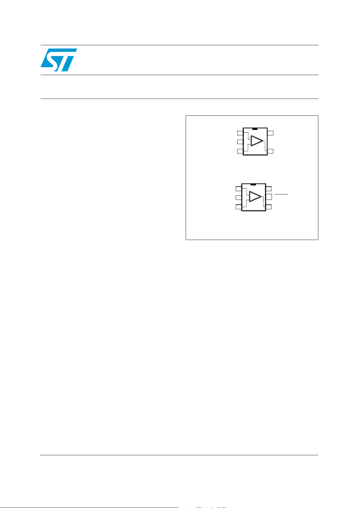
The TSV6290 and the TSV6291 are single
operational amplifiers with a high bandwidth while
consuming only 29 µA. They must be used in a
gain configuration (G<-3, G>+4).
V
In+
In+
1
1
+
+
_
V
V
CC-
CC-
In-
In-
_
2
2
3
3
V
5
5
CC+
CC+
4
4
Out
Out
TSV6291ICT/ILT
SC70-5/SOT23-5
In+
1
+
V
CC-
In-
_
2
3
6
5
4
V
CC+
SHDN
Out
TSV6290ICT/ILT
SC70-6/SOT23-6
The TSV6290 comes with a shutdown function.
The TSV6290 and TSV6291 present a high
tolerance to ESD, sustaining 4 kV for the human
body model.
Additionally, the TSV6290 and TSV6291 are
offered in SC70-5/6 and SOT23-5/6
micropackages, with extended temperature
ranges from -40° C to +125° C.
All these features make the TSV629x ideal for
sensor interfaces, battery-supplied and portable
applications, as well as active filtering.
With a very low input bias current and low offset
voltage (800 µV maximum for the A version), the
TSV629x family of devices is ideal for applications
requiring precision. The devices can operate at a
power supply ranging from 1.5 to 5.5 V, and
therefore suit battery-powered devices, extending
battery life.
March 2010 Doc ID 17117 Rev 1 1/23
www.st.com
23

Contents TSV6290, TSV6290A, TSV6291, TSV6291A
Contents
1 Absolute maximum ratings and operating conditions . . . . . . . . . . . . . 3
2 Electrical characteristics . . . . . . . . . . . . . . . . . . . . . . . . . . . . . . . . . . . . . 4
3 Application information . . . . . . . . . . . . . . . . . . . . . . . . . . . . . . . . . . . . . 12
3.1 Operating voltages . . . . . . . . . . . . . . . . . . . . . . . . . . . . . . . . . . . . . . . . . . 12
3.2 Rail-to-rail input . . . . . . . . . . . . . . . . . . . . . . . . . . . . . . . . . . . . . . . . . . . . 12
3.3 Rail-to-rail output . . . . . . . . . . . . . . . . . . . . . . . . . . . . . . . . . . . . . . . . . . . 12
3.4 Shutdown function (TSV6290) . . . . . . . . . . . . . . . . . . . . . . . . . . . . . . . . . 12
3.5 Optimization of DC and AC parameters . . . . . . . . . . . . . . . . . . . . . . . . . . 14
3.6 Driving resistive and capacitive loads . . . . . . . . . . . . . . . . . . . . . . . . . . . 14
3.7 PCB layouts . . . . . . . . . . . . . . . . . . . . . . . . . . . . . . . . . . . . . . . . . . . . . . . 14
3.8 Macromodel . . . . . . . . . . . . . . . . . . . . . . . . . . . . . . . . . . . . . . . . . . . . . . . 14
4 Package information . . . . . . . . . . . . . . . . . . . . . . . . . . . . . . . . . . . . . . . . 15
4.1 SOT23-5 package mechanical data . . . . . . . . . . . . . . . . . . . . . . . . . . . . . 16
4.2 SOT23-6 package mechanical data . . . . . . . . . . . . . . . . . . . . . . . . . . . . . 17
4.3 SC70-5 (or SOT323-5) package mechanical data . . . . . . . . . . . . . . . . . . 18
4.4 SC70-6 (or SOT323-6) package mechanical data . . . . . . . . . . . . . . . . . . 19
5 Ordering information . . . . . . . . . . . . . . . . . . . . . . . . . . . . . . . . . . . . . . . 21
6 Revision history . . . . . . . . . . . . . . . . . . . . . . . . . . . . . . . . . . . . . . . . . . . 22
2/23 Doc ID 17117 Rev 1
TSV6290, TSV6290A, TSV6291, TSV6291A Absolute maximum ratings and operating conditions
1 Absolute maximum ratings and operating conditions
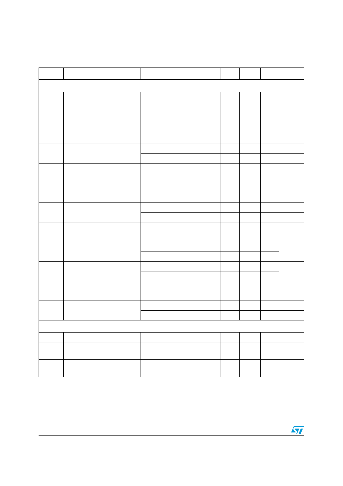
Table 1. Absolute maximum ratings (AMR)
Symbol Parameter Value Unit
(3)
(4)
(1)
(3)
(8)
(2)
(7)
(9)
(5)(6)
V
V
CC-
CC-
6V
±V
CC
-0.2 to V
+0.2 V
CC+
V
10 mA
-0.2 to V
+0.2 V
CC+
205
250
°C/W
240
232
4kV
300 V
1.5 kV
V
CC
V
V
I
in
Supply voltage
Differential input voltage
id
Input voltage
in
Input current
SHDN Shutdown voltage
T
stg
Storage temperature -65 to +150 °C
Thermal resistance junction to ambient
SC70-5
R
thja
SOT23-5
SOT23-6
SC70-6
T
Maximum junction temperature 150 °C
j
HBM: human body model
ESD
MM: machine model
CDM: charged device model
Latch-up immunity 200 mA
1. All voltage values, except differential voltage, are with respect to network ground terminal.
2. Differential voltages are the non-inverting input terminal with respect to the inverting input terminal.
3. Vcc-Vin must not exceed 6 V, Vin must not exceed 6 V.
4. Input current must be limited by a resistor in series with the inputs.
5. Short-circuits can cause excessive heating and destructive dissipation.
are typical values.
6. R
th
7. Human body model: 100 pF discharged through a 1.5 kΩ resistor between two pins of the device, done for
all couples of pin combinations with other pins floating.
8. Machine mode: a 200 pF capacitor is charged to the specified voltage, then discharged directly between
two pins of the device with no external series resistor (internal resistor < 5 Ω), done for all couples of pin
combinations with other pins floating.
9. Charged device model: all pins plus package are charged together to the specified voltage and then
discharged directly to the ground.
Table 2. Operating conditions
Symbol Parameter Value Unit
V
V
T
CC
icm
oper
Supply voltage 1.5 to 5.5 V
Common mode input voltage range V
CC-
-0.1 to V
+0.1 V
CC+
Operating free air temperature range -40 to +125 °C
Doc ID 17117 Rev 1 3/23
Electrical characteristics TSV6290, TSV6290A, TSV6291, TSV6291A
2 Electrical characteristics
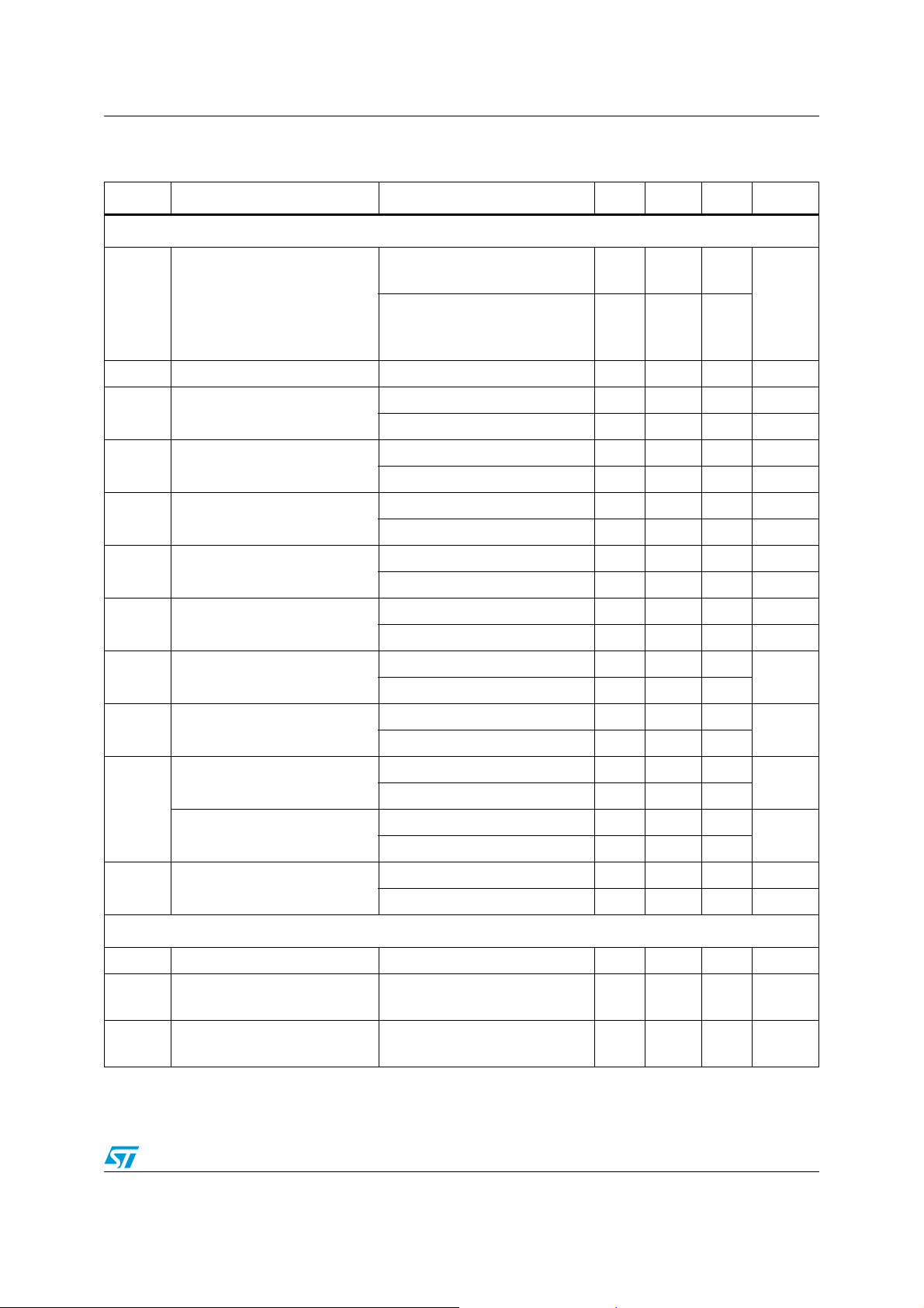
Table 3. Electrical characteristics at V
Symbol Parameter Conditions Min. Typ. Max. Unit
DC performance
and R
= +1.8 V with V
connected to VCC/2 (unless otherwise specified)
L
CC+
= 0 V, V
CC-
= VCC/2, T
icm
= 25° C,
amb
V
DV
CMR
A
V
V
Offset voltage
io
Input offset voltage drift 2 μV/°C
io
Input offset current
I
io
(V
out=VCC
Input bias current
I
ib
(V
out=VCC
Common mode rejection ratio
20 log (ΔV
Large signal voltage gain
vd
High level output voltage
OH
Low level output voltage
OL
Isink
I
out
Isource
I
Supply current (per operator)
CC
AC performance
/2)
/2)
/ΔVio)
ic
(1)
(1)
TSV6290-TSV6291
TSV6290A-TSV6291A
< Top < T
T
min
max
TSV6290-TSV6291
TSV6290A-TSV6291A
< Top < T
T
min
max
< Top < T
T
min
0 V to 1.8 V, V
< Top < T
T
min
R
= 10 kΩ, V
L
< Top < T
T
min
R
=10kΩ 35 5
L
< Top < T
T
min
max
= 0.9 V 53 74
out
max
= 0.5 V to 1.3 V 78 95
out
max
max
51
73
50
110
1100
110
1100
4
0.8
mV
6
2
pA
pA
dB
dB
mV
RL=10kΩ 435
mV
< Top < T
T
min
V
= 1.8 V 6 12
out
< Top < T
T
min
V
= 0 V 6 10
out
< Top < T
T
min
No load, V
< Top < T
T
min
max
max
max
out=VCC
max
4
4
/2 25 31
50
mA
mA
µA
33
GBP Gain bandwidth product RL=10kΩ, CL= 100 pF 1.1 MHz
Gain Minimum gain for stability
SR Slew rate
1. Guaranteed by design.
Phase margin = 60°, Rf = 10 kΩ,
=10kΩ, CL=20pF
R
L
RL=10kΩ, CL= 100 pF,
Vout = 0.5 V to 1.3 V
+4
-3
0.33 V/μs
4/23 Doc ID 17117 Rev 1
V/V
TSV6290, TSV6290A, TSV6291, TSV6291A Electrical characteristics
Table 4. Shutdown characteristics VCC= 1.8 V (TSV6290)
Symbol Parameter Conditions Min. Typ. Max. Unit
DC performance
I
CC
t
on
t
off
V
V
I
IH
I
IL
I
OLeak
SHDN = V
Supply current in shutdown
mode (all operators)
Amplifier turn-on time
Amplifier turn-off time
SHDN logic high 1.3 V
IH
SHDN logic low 0.5 V
IL
T
T
R
V
R
V
min
min
L
CC-
L
CC+
SHDN current high SHDN =V
SHDN current low SHDN =V
Output leakage in shutdown
mode
SHDN
T
min
CC-
< Top < 85° C 200 nA
< Top < 125° C 1.5 µA
=5kΩ, V
out=VCC-
to
+0.2V
=5kΩ, V
out=VCC+
- 0.5 to
-0.7V
CC+
CC-
=V
CC-
< Top < T
max
2.5 50 nA
300 ns
30 ns
10 pA
10 pA
50 pA
1nA
Doc ID 17117 Rev 1 5/23
Electrical characteristics TSV6290, TSV6290A, TSV6291, TSV6291A
Table 5. V
CC+
= +3.3 V, V
= 0 V, V
CC-
= VCC/2, T
icm
= 25° C, RL connected to VCC/2
amb
(unless otherwise specified)
Symbol Parameter Min. Typ. Max. Unit
DC performance
V
DV
CMR
A
V
V
Offset voltage
io
Input offset voltage drift 2 μV/°C
io
I
Input offset current
io
I
Input bias current
ib
Common mode rejection ratio
20 log (ΔV
Large signal voltage gain
vd
High level output voltage
OH
Low level output voltage
OL
Isink
I
out
Isource
I
Supply current (per operator)
CC
AC performance
/ΔVio)
ic
(1)
(1)
TSV6290-TSV6291
TSV6290A-TSV6291A
< Top < T
T
min
max
TSV6290-TSV6291
TSV6290A-TSV6291A
110pA
T
min
< Top < T
max
1 100 pA
110pA
T
< Top < T
min
0V to 3.3V, V
T
< Top < T
min
R
=10 kΩ, V
T
L
min
out
< Top < T
max
= 1.65 V 57 79 dB
out
max
53 dB
= 0.5 V to 2.8 V 81 98 dB
max
76 dB
1 100 pA
RL=10kΩ 35 5
< Top < T
T
min
R
=10kΩ 435
L
< Top < T
T
min
V
= 5 V 23 45
out
< Top < T
T
min
V
= 0 V 23 38
out
< Top < T
T
min
No load, V
T
< Top < T
min
max
max
max
max
=2.5V 26 33 µA
out
max
50
20
20
4
0.8
6
2
50
35 µA
mV
mV
mV
mA
mA
GBP Gain bandwidth product RL=10kΩ, CL= 100 pF 1.2 MHz
Gain Minimum gain for stability
SR Slew rate
1. Guaranteed by design.
Phase margin = 60°, Rf = 10 kΩ,
RL=10kΩ, CL=20pF
RL=10kΩ, CL= 100 pF,
= 0.5 V to 2.8 V
V
out
+4
-3
0.4 V/μs
6/23 Doc ID 17117 Rev 1
V/V
TSV6290, TSV6290A, TSV6291, TSV6291A Electrical characteristics
Table 6. V
CC+
= +5 V, V
= 0 V, V
CC-
= VCC/2, T
icm
= 25° C, RL connected to VCC/2
amb
(unless otherwise specified)
Symbol Parameter Min. Typ. Max. Unit
DC performance
V
DV
CMR
SVR
A
V
V
I
I
Offset voltage
io
Input offset voltage drift 2 μV/°C
io
I
Input offset current
io
I
Input bias current
ib
Common mode rejection ratio
20 log (ΔV
Supply voltage rejection ratio 20
log (ΔVCC/ΔVio)
Large signal voltage gain
vd
High level output voltage
OH
Low level output voltage
OL
I
sink
out
I
source
Supply current (per operator)
CC
AC performance
/ΔVio)
ic
(1)
(1)
TSV6290-TSV6291
TSV6290A-TSV6291A
< Top < T
T
min
max
TSV6290-TSV6291
TSV6290A-TSV6291A
110pA
T
min
< Top < T
max
1 100 pA
110pA
T
< Top < T
min
0V to 5V, V
T
< Top < T
min
= 1.8 to 5 V 75 102 dB
V
CC
< Top < T
T
min
RL=10 kΩ, V
< Top < T
T
min
R
=10kΩ 35 7
L
< Top < T
T
min
R
=10kΩ 635
L
< Top < T
T
min
V
=5V 40 69
out
< Top < T
T
min
V
= 0 V 40 74
out
< Top < T
T
min
No load, V
< Top < T
T
min
max
= 2.5 V 60 80 dB
out
max
max
= 0.5 V to 4.5 V 85 98 dB
out
max
max
max
max
max
=2.5V 30 36 µA
out
max
55
73
80
50
35
35
1 100 pA
4
0.8
6
2
50
38 µA
mV
mV
mV
mA
mA
GBP Gain bandwidth product R
Gain Minimum gain for stability
SR Slew rate
=10kΩ, CL= 100 pF 1.3 MHz
L
Phase margin = 60°, Rf = 10 kΩ,
RL=10kΩ, CL=20pF
RL=10kΩ, CL= 100 pF,
= 0.5 V to 4.5 V
V
out
+4
-3
V/V
0.5 V/μs
Doc ID 17117 Rev 1 7/23
 Loading...