

TSV620, TSV620A, TSV621, TSV621A
Rail-to-rail input/output 29 µA 420 kHz CMOS operational amplifiers
Features
VCC
6
6
5
4
4
5
5
5
4
4
4
VCC
Out
Out
V
CC+
SHDN
Out
■ Low supply voltage: 1.5 V–5.5 V
■ Rail-to-rail input and output
■ Low input offset voltage: 800 µV max (A
version)
■ Low power consumption: 29 µA typ
■ Low power shutdown mode: 5nA typ (TSV620)
■ Gain bandwidth product: 420 kHz typ
■ Unity gain stability
■ Micropackages: SC70-5/6, SOT23-5/6
■ Low input bias current: 1 pA typ
■ Extended temperature range: -40 to +125° C
■ 4kV HBM
Applications
In+
In+
1
1
1
+
+
+
_
_
_
2
2
2
VDD
VDD
In-
In-
3
3
3
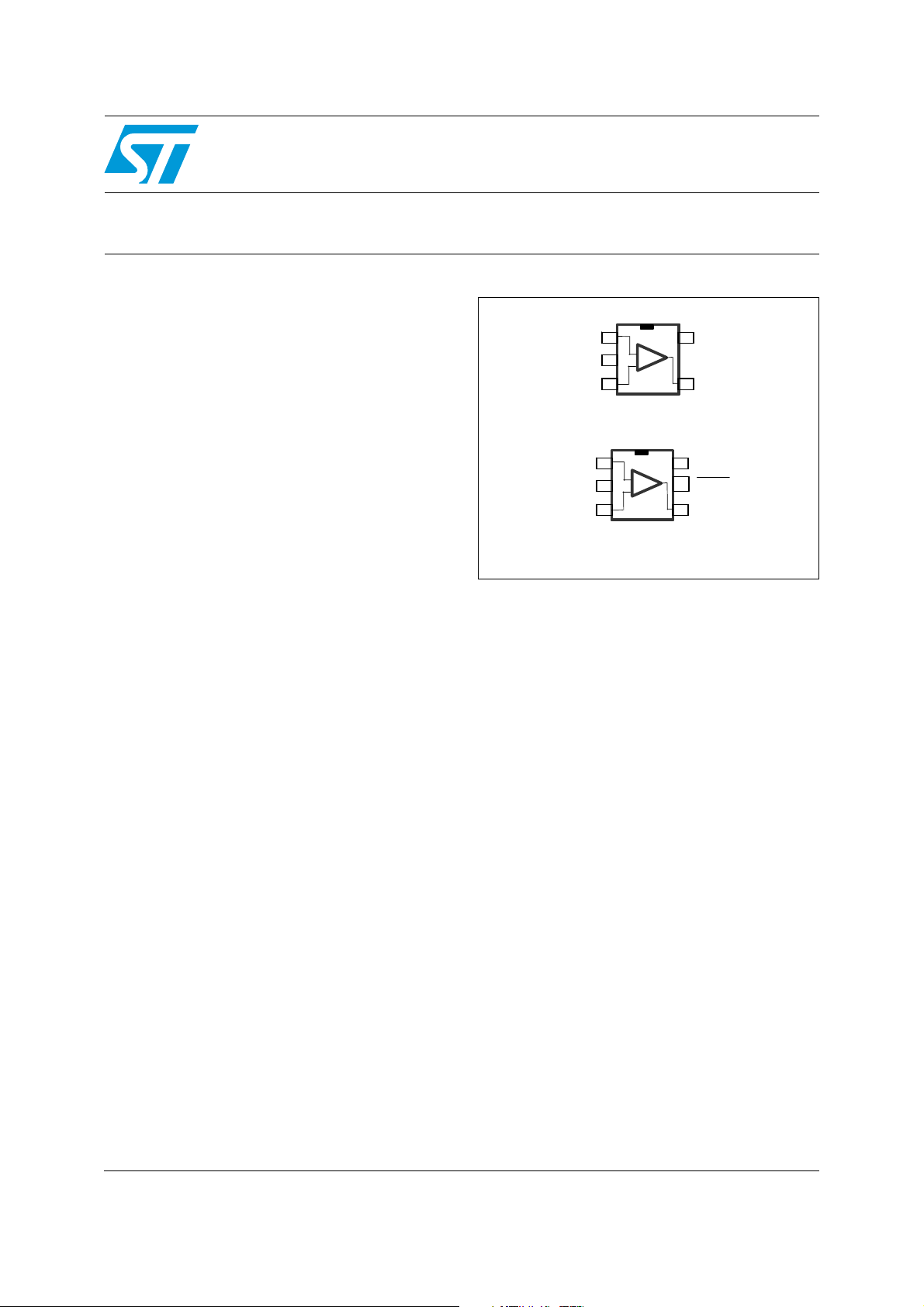
TSV621ICT/ILT
SC70-5/SOT23-5
In+
1
1
+
+
_
V
CC-
In-
_
2
2
3
3
TSV620ICT/ILT
SC70-6/SOT23-6
This product features an excellent speed/power
consumption ratio, offering a 420 kHz gain
bandwidth while consuming only 29 µA at a
5 V supply voltage.
■ Battery-powered applications
■ Portable devices
■ Signal conditioning
■ Active filtering
■ Medical instrumentation
Description
The TSV620 and TSV621 are single operational
amplifiers offering low voltage, low power
operation and rail-to-rail input and output.
With a very low input bias current and low offset
voltage (800 µV maximum for the A version), the
TSV62x is ideal for applications requiring
precision. The device can operate at a power
supply ranging from 1.5 to 5.5 V, and therefore
suits battery-powered devices and extends their
battery life.
These operational amplifiers are unity gain stable
for capacitive loads up to 100 pF.
The device is internally adjusted to provide very
narrow dispersion of AC and DC parameters,
especially power consumption, product gain
bandwidth and slew rate.
The TSV62x presents a high tolerance to ESD,
sustaining 4 kV for the human body model.
The devices are offered in macropackages,
SC70-6 and SOT23-6 for the TSV620 and
SC70-5 and SOT23-5 for the TSV621. They are
guaranteed for industrial temperature ranges from
-40° C to +125° C.
All these features make the TSV620 and TSV621
ideal for sensor interfaces, battery-supplied and
portable applications, as well as active filtering.
October 2009 Doc ID 14912 Rev 2 1/24
www.st.com
24

Contents TSV620, TSV620A, TSV621, TSV621A
Contents
1 Absolute maximum ratings and operating conditions . . . . . . . . . . . . . 3
2 Electrical characteristics . . . . . . . . . . . . . . . . . . . . . . . . . . . . . . . . . . . . . 4
3 Application information . . . . . . . . . . . . . . . . . . . . . . . . . . . . . . . . . . . . . 12
3.1 Operating voltages . . . . . . . . . . . . . . . . . . . . . . . . . . . . . . . . . . . . . . . . . . 12
3.2 Rail-to-rail input . . . . . . . . . . . . . . . . . . . . . . . . . . . . . . . . . . . . . . . . . . . . 12
3.3 Rail-to-rail output . . . . . . . . . . . . . . . . . . . . . . . . . . . . . . . . . . . . . . . . . . . 12
3.4 Shutdown function (TSV620) . . . . . . . . . . . . . . . . . . . . . . . . . . . . . . . . . . 13
3.5 Optimization of DC and AC parameters . . . . . . . . . . . . . . . . . . . . . . . . . . 14
3.6 Driving resistive and capacitive loads . . . . . . . . . . . . . . . . . . . . . . . . . . . 14
3.7 PCB layouts . . . . . . . . . . . . . . . . . . . . . . . . . . . . . . . . . . . . . . . . . . . . . . . 14
3.8 Macromodel . . . . . . . . . . . . . . . . . . . . . . . . . . . . . . . . . . . . . . . . . . . . . . . 15
4 Package information . . . . . . . . . . . . . . . . . . . . . . . . . . . . . . . . . . . . . . . . 16
4.1 SOT23-5 package mechanical data . . . . . . . . . . . . . . . . . . . . . . . . . . . . . 17
4.2 SOT23-6 package mechanical data . . . . . . . . . . . . . . . . . . . . . . . . . . . . . 18
4.3 SC70-5 (or SOT323-5) package mechanical data . . . . . . . . . . . . . . . . . . 19
4.4 SC70-6 (or SOT323-6) package mechanical data . . . . . . . . . . . . . . . . . . 20
5 Ordering information . . . . . . . . . . . . . . . . . . . . . . . . . . . . . . . . . . . . . . . 22
6 Revision history . . . . . . . . . . . . . . . . . . . . . . . . . . . . . . . . . . . . . . . . . . . 23
2/24 Doc ID 14912 Rev 2

TSV620, TSV620A, TSV621, TSV621A Absolute maximum ratings and operating conditions
1 Absolute maximum ratings and operating conditions
Table 1. Absolute maximum ratings (AMR)
Symbol Parameter Value Unit
(3)
(4)
(1)
(5)
(9)
(2)
(8)
(10)
(6)(7)
V
V
CC-
CC-
6V
±V
CC
-0.2 to V
+0.2 V
CC+
V
10 mA
-0.2 to V
+0.2 V
CC+
205
250
°C/W
240
232
4kV
300 V
1.5 kV
V
CC
V
id
V
in
I
in
SHDN
T
stg
R
thja
T
j
ESD
Supply voltage
Differential input voltage
Input voltage
Input current
Shutdown voltage
Storage temperature -65 to +150 °C
Thermal resistance junction to ambient
SC70-5
SOT23-5
SOT23-6
SC70-6
Maximum junction temperature 150 °C
HBM: human body model
MM: machine model
CDM: charged device model
Latch-up immunity 200 mA
1. All voltage values, except differential voltage are with respect to network ground terminal.
2. Differential voltages are the non-inverting input terminal with respect to the inverting input terminal.
3. Vcc-Vin must not exceed 6 V.
4. Input current must be limited by a resistor in series with the inputs.
5. Vcc-SHDN must not exceed 6 V.
6. Short-circuits can cause excessive heating and destructive dissipation.
are typical values.
7. R
th
8. Human body model: 100 pF discharged through a 1.5 kΩ resistor between two pins of the device, done for
all couples of pin combinations with other pins floating.
9. Machine mode: a 200 pF capacitor is charged to the specified voltage, then discharged directly between
two pins of the device with no external series resistor (internal resistor < 5
combinations with other pins floating.
10. Charged device model: all pins plus package are charged together to the specified voltage and then
discharged directly to the ground.
Table 2. Operating conditions
Ω), done for all couples of pin
Symbol Parameter Value Unit
T
V
V
CC
icm
oper
Supply voltage 1.5 to 5.5 V
Common mode input voltage range V
CC-
-0.1 to V
+0.1 V
CC+
Operating free air temperature range -40 to +125 °C
Doc ID 14912 Rev 2 3/24
Electrical characteristics TSV620, TSV620A, TSV621, TSV621A
2 Electrical characteristics
Table 3. Electrical characteristics at V
Symbol Parameter Conditions Min. Typ. Max. Unit
DC performance
and R
= +1.8 V with VDD = 0 V, V
connected to VCC/2 (unless otherwise specified)
L
CC+
= VCC/2, Top = 25° C,
icm
V
DV
CMR
A
V
V
Offset voltage
io
Input offset voltage drift 2 μV/°C
io
Input offset current
I
io
(V
out=VCC
Input bias current
I
ib
(V
out=VCC
Common mode rejection ratio
20 log (
Large signal voltage gain
vd
High level output voltage
OH
Low level output voltage
OL
Isink
I
out
Isource
I
Supply current (per operator)
CC
AC performance
ΔV
/2)
/2)
/ΔVio)
ic
TSV62x
TSV62xA
T
< Top < T
min
max
0.8
TSV62x
TSV62xA
2.8
110
T
< Top < T
min
max
1100
110
T
< Top < T
min
0 V to 1.8 V, V
< Top < T
T
min
R
= 10 kΩ, V
L
< Top < T
T
min
R
=10kΩ 35 5
L
< Top < T
T
min
=10kΩ 435
R
L
< Top < T
T
min
= 1.8 V 6 12
V
o
< Top < T
T
min
V
= 0 V 6 10
o
< Top < T
T
min
No load, V
< Top < T
T
min
max
= 0.9 V 53 74
out
max
= 0.5 V to 1.3 V 78 95
out
max
max
max
max
max
out=VCC
/2 25 31
max
51
73
50
4
4
1100
50
33
4
mV
6
(1)
pA
(1)
pA
dB
dB
mV
mV
mA
mA
µA
R
=10kΩ, CL= 100 pF,
GBP Gain bandwidth product
F
Unity gain frequency RL=10kΩ, CL= 100 pF 280 kHz
u
φmPhase margin R
G
Gain margin RL=10kΩ, CL= 100 pF 9 dB
m
SR Slew rate R
1. Guaranteed by design.
L
f=100kHz
=10kΩ, CL= 100 pF 45 Degrees
L
=10kΩ, CL= 100 pF, Av = 1 0.084 0.11 0.14 V/μs
L
4/24 Doc ID 14912 Rev 2
275 340 kHz

TSV620, TSV620A, TSV621, TSV621A Electrical characteristics
Table 4. Shutdown characteristics VCC=1.8V
Symbol Parameter Conditions Min. Typ. Max. Unit
DC performance
I
CC
t
on
t
off
V
V
I
IH
I
IL
I
OLeak
= V
Supply current in shutdown
mode
(all operators)
Amplifier turn-on time
Amplifier turn-off time
SHDN logic high 1.3 V
IH
SHDN logic low 0.5 V
IL
SHDN
T
min
T
min
R
L
+0.2
R
L
V
CC+
SHDN current high SHDN =V
SHDN current low SHDN =V
Output leakage in shutdown
mode
SHDN
T
min
CC-
< Top < 85° C 200 nA
< Top < 125° C 1.5 µA
=2kΩ, V
=2kΩ, V
out=VCC-
out=VCC+
to V
CC
-0.5 to
+ 0.7
CC+
CC-
=V
CC-
< Top < 125° C 1 nA
2.5 50 nA
300 ns
30 ns
10 pA
10 pA
50 pA
Doc ID 14912 Rev 2 5/24
Electrical characteristics TSV620, TSV620A, TSV621, TSV621A
Table 5. V
CC+
= +3.3 V, V
= 0 V, V
CC-
= VCC/2, Top = 25° C, RL connected to VCC/2
icm
(unless otherwise specified)
Symbol Parameter Min. Typ. Max. Unit
DC performance
V
DV
CMR
A
V
V
Offset voltage
io
Input offset voltage drift 2 μV/°C
io
I
Input offset current
io
I
Input bias current
ib
Common mode rejection ratio
20 log (
Large signal voltage gain
vd
High level output voltage
OH
Low level output voltage
OL
Isink
I
out
Isource
I
Supply current (per operator)
CC
AC performance
ΔV
/ΔVio)
ic
TSV62x
TSV62xA
< Top < T
T
min
max
TSV62x
TSV62xA
110
T
min
< Top < T
max
1 100 pA
110
T
< Top < T
min
0V to 3.3V, V
T
< Top < T
min
R
=10 kΩ, V
L
< Top < T
T
min
=10kΩ 35 5
R
L
< Top < T
T
min
R
=10kΩ 435
L
< Top < T
T
min
V
= 5 V 30 45
o
< Top < T
T
min
= 0 V 30 38
V
o
< Top < T
T
min
No load, V
T
< Top < T
min
max
= 1.75 V 57 79 dB
out
max
= 0.5 V to 2.8 V 81 98 dB
out
max
max
max
max
max
=2.5V 26 33 µA
out
max
53 dB
76 dB
50
25
25
1 100 pA
4
0.8
6
2.8
(1)
(1)
50
35 µA
mV
pA
pA
mV
mV
mA
mA
R
=10kΩ, CL= 100 pF,
GBP Gain bandwidth product
Unity gain frequency RL = 10 kΩ, CL= 100 pF 310 kHz
F
u
φmPhase margin R
G
Gain margin RL = 10 kΩ, CL= 100 pF 9 dB
m
SR Slew rate R
1. Guaranteed by design.
L
f = 100 kHz
= 10 kΩ, CL= 100 pF 45 Degrees
L
=10kΩ, CL= 100 pF, AV= 1 0.094 0.12 V/μs
L
6/24 Doc ID 14912 Rev 2
310 380 kHz
TSV620, TSV620A, TSV621, TSV621A Electrical characteristics
Table 6. V
CC+
= +5 V, V
= 0 V, V
CC-
= VCC/2, Top = 25° C, RL connected to VCC/2
icm
(unless otherwise specified)
Symbol Parameter Min. Typ. Max. Unit
DC performance
V
DV
CMR
SVR
A
V
V
I
I
Offset voltage
io
Input offset voltage drift 2 μV/°C
io
I
Input offset current
io
I
Input bias current
ib
Common mode rejection ratio
20 log (
Supply voltage rejection ratio 20
log (
ΔV
Large signal voltage gain
vd
High level output voltage
OH
Low level output voltage
OL
I
sink
out
I
source
Supply current (per operator)
CC
AC performance
ΔV
CC
/ΔVio)
ic
/ΔVio)
TSV62x
TSV62xA
< Top < T
T
min
max
TSV62x
TSV62xA
110
T
min
< Top < T
max
1 100 pA
110
T
< Top < T
min
0V to 5V, V
T
< Top < T
min
V
= 1.8 to 5 V 75 102 dB
CC
< Top < T
T
min
=10 kΩ, V
R
L
< Top < T
T
min
R
=10kΩ 35 7
L
< Top < T
T
min
R
=10kΩ 635
L
< Top < T
T
min
max
= 2.5 V 60 80 dB
out
max
max
= 0.5 V to 4.5 V 85 98 dB
out
max
max
max
55
73
80
50
1 100 pA
Vo =5V 40 69
T
min
< Top < T
max
35 65
Vo = 0 V 40 74
< Top < T
T
min
No load, V
< Top < T
T
min
max
=2.5V 29 36 µA
out
max
35 68
4
0.8
6
2.8
(1)
(1)
50
38 µA
mV
pA
pA
mV
mV
mA
mA
GBP Gain bandwidth product
F
Unity gain frequency RL = 10 kΩ, CL= 100 pF 360 kHz
u
φm Phase margin R
G
Gain margin RL = 10 kΩ, CL= 100 pF 9 dB
m
SR Slew rate R
=10kΩ, CL= 100 pF,
R
L
f = 100 kHz
= 10 kΩ, CL= 100 pF 45 Degrees
L
=10kΩ, CL= 100 pF, AV= 1 0.108 0.14 V/μs
L
350 420 kHz
Doc ID 14912 Rev 2 7/24

Electrical characteristics TSV620, TSV620A, TSV621, TSV621A
Table 6. V
= +5 V, V
CC+
= 0 V, V
CC-
= VCC/2, Top = 25° C, RL connected to VCC/2
icm
(unless otherwise specified) (continued)
Symbol Parameter Min. Typ. Max. Unit
e
Equivalent input noise voltage f = 1 kHz 70
n
THD Total harmonic distortion
1. Guaranteed by design.
Table 7. Shutdown characteristics VCC=5V
Av = 1, f = 1 kHz, R
V
= Vcc/2, V
icm
Symbol Parameter Conditions Min. Typ. Max. Unit
DC performance
= V
I
CC
t
on
t
off
V
V
I
IH
I
IL
I
OLeak
SHDN
Supply current in shutdown
mode (all operators)
Amplifier turn-on time
Amplifier turn-off time
SHDN logic high 4.5 V
IH
SHDN logic low 0.5 V
IL
T
T
R
0.2
R
V
min
min
L
L
CC+
SHDN current high SHDN =V
SHDN current low SHDN =V
Output leakage in shutdown
mode
SHDN
T
min
CC-
< Top < 85° C 200 nA
< Top < 125° C 1.5 µA
=2kΩ, V
=2kΩ, V
out=VCC-
out=VCC+
+ 0.7
CC+
CC-
=V
CC-
< Top < 125° C 1 nA
out
= 100 kΩ,
L
= 2 V
pp
to V
- 0.5 to
CC-
0.004 %
550 nA
+
300 ns
30 ns
10 pA
10 pA
50 pA
nV
-----------Hz
8/24 Doc ID 14912 Rev 2
 Loading...