

TSV611, TSV611A, TSV612, TSV612A
Features
■ Rail-to-rail input and output
■ Low power consumption: 10 µA typ at 5 V
■ Low supply voltage: 1.5 to 5.5 V
■ Gain bandwidth product: 120 kHz typ
■ Unity gain stable
■ Low input offset voltage: 800 µV max (A
version)
■ Low input bias current: 1 pA typ
■ Temperature range: -40 to +85° C
Applications
■ Battery-powered applications
■ Smoke detectors
■ Proximity sensors
■ Portable devices
■ Signal conditioning
■ Active filtering
■ Medical instrumentation
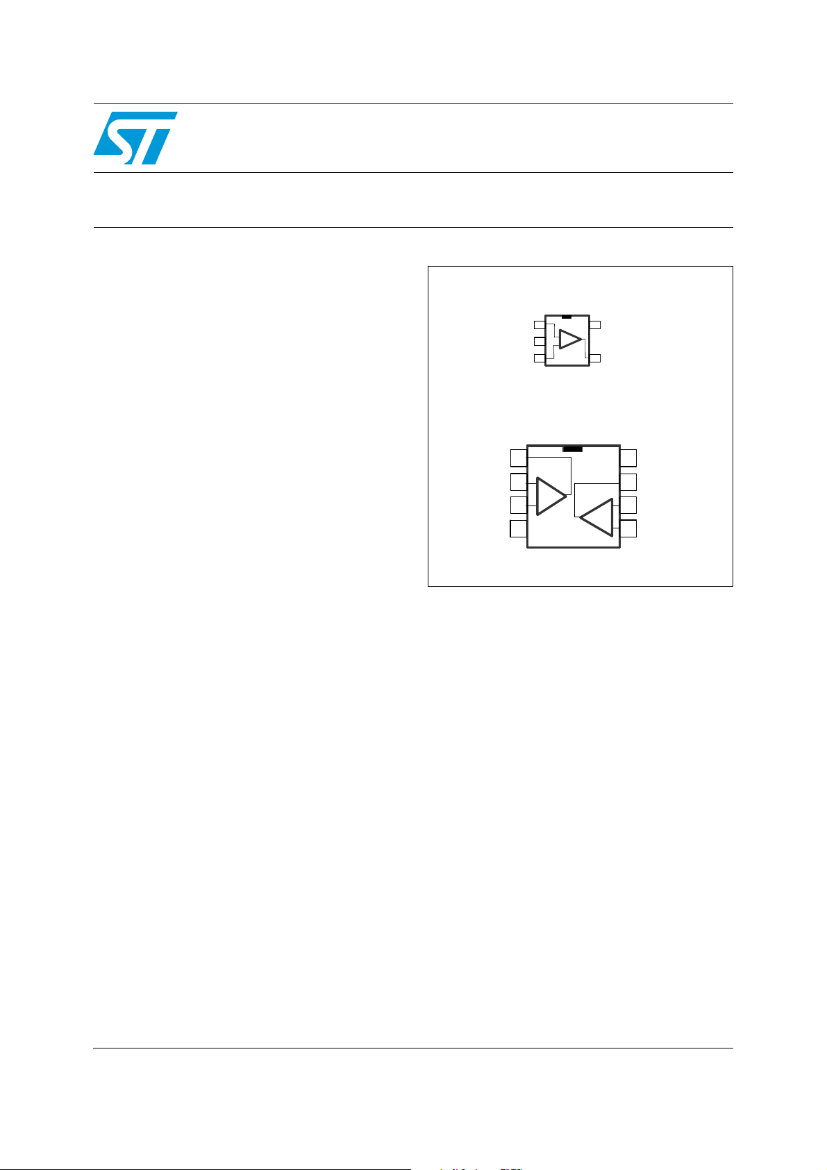
Rail-to-rail input/output 10 µA, 120 kHz
CMOS operational amplifiers
TSV611ILT - TSV611ICT
V
In+
In+
1
1
+
+
_
V
V
CC-
CC-
In-
In-
_
2
2
3
3
SOT23-5/SC70-5
TSV612IST - TSV612ID/DT
Out1
Out1
1
1
_
In1-
In1-
In1+
In1+
V
V
CC-
CC-
_
2
2
+
+
3
3
4
4
MiniSO-8/SO-8
V
5
5
CC+
CC+
4
4
Out
Out
8
8
V
V
CC+
CC+
7
7
Out2
Out2
_
_
+
+
In2-
In2-
6
6
In2+
In2+
5
5
Description
The TSV61x family of single and dual operational
amplifiers offers low voltage, low power operation
and rail-to-rail input and output.
The devices also feature an ultra-low input bias
current as well as a low input offset voltage.
The TSV61x have a gain bandwidth product of
120 kHz while consuming only 10 µA at 5 V.
These features make the TSV61x family ideal for
sensor interfaces, battery supplied and portable
applications, as well as active filtering.
January 2010 Doc ID 15768 Rev 2 1/19
www.st.com
19
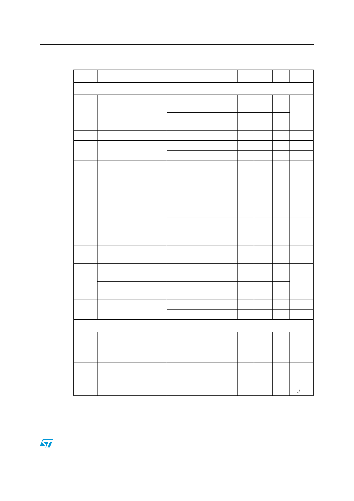
Absolute maximum ratings and operating conditions TSV611, TSV611A, TSV612, TSV612A
1 Absolute maximum ratings and operating conditions
Table 1. Absolute maximum ratings
Symbol Parameter Value Unit
(3)
(1)
(7)
(2)
(6)
(8)
(4)(5)
V
CC-
6V
±V
CC
-0.2 to V
+0.2 V
CC+
V
°C/W
4kV
200 V
1.5 kV
V
CC
V
V
T
stg
Supply voltage
Differential input voltage
id
Input voltage
in
Storage temperature -65 to +150 °C
Thermal resistance junction to ambient
SC70-5 205
R
thja
SOT23-5 250
MiniSO-8 190
SO-8 125
T
Maximum junction temperature 150 °C
j
HBM: human body model
ESD
MM: machine model
CDM: charged device model
Latch-up immunity 200 mA
1. All voltage values, except differential voltage are with respect to network ground terminal.
2. Differential voltages are the non-inverting input terminal with respect to the inverting input terminal.
3. Vcc-Vin must not exceed 6 V.
4. Short-circuits can cause excessive heating and destructive dissipation.
5. Rth are typical values.
6. Human body model: 100 pF discharged through a 1.5 kΩ resistor between two pins of the device, done for
all couples of pin combinations with other pins floating.
7. Machine model: a 200 pF cap is charged to the specified voltage, then discharged directly between two
pins of the device with no external series resistor (internal resistor < 5 Ω), done for all couples of pin
combinations with other pins floating.
8. Charged device model: all pins plus package are charged together to the specified voltage and then
discharged directly to ground.
Table 2. Operating conditions
Symbol Parameter Value Unit
T
V
V
CC
icm
oper
Supply voltage 1.5 to 5.5 V
Common mode input voltage range V
Operating free air temperature range -40 to +85 °C
2/19 Doc ID 15768 Rev 2
CC-
-0.1 to V
+0.1 V
CC+
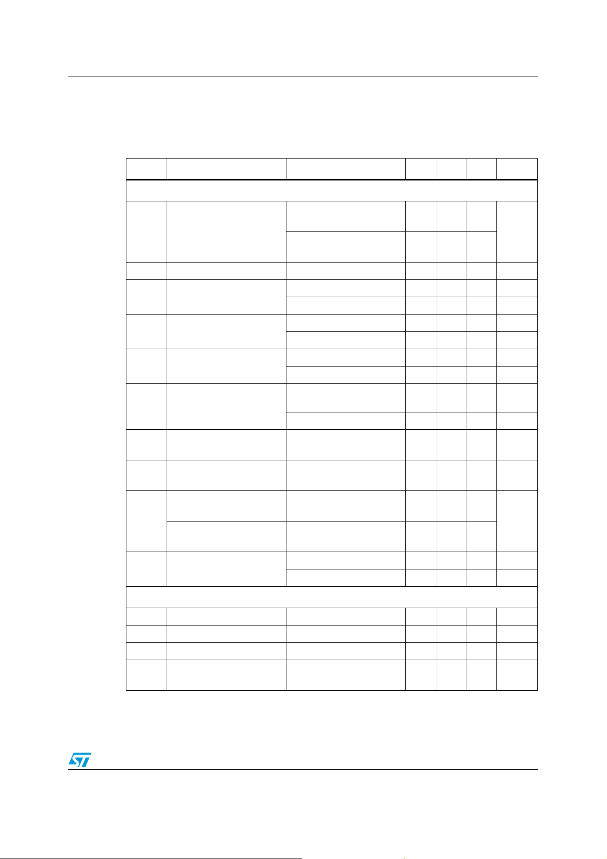
TSV611, TSV611A, TSV612, TSV612A Electrical characteristics
2 Electrical characteristics
Table 3. Electrical characteristics at V
with V
= 0 V, V
CC-
= VCC/2, T
icm
(unless otherwise specified)
Symbol Parameter Conditions Min. Typ. Max. Unit
DC performance
= +1.8 V
CC+
= 25° C, and RL connected to VCC/2
amb
V
Offset voltage
io
DV
CMR
V
V
Input offset voltage drift 2 μV/°C
io
Input offset current
I
io
(V
out=Vcc
Input bias current
I
ib
(V
out=Vcc
Common mode rejection
ratio 20 log (ΔVic/ΔVio)
Large signal voltage gain
A
vd
High level output voltage
OH
Low level output voltage
OL
Isink
I
out
Isource
Supply current (per
I
CC
operator)
AC performance
/2)
/2)
TSV61x
TSV61xA
< Top < T
T
min.
< Top < T
T
min.
T
< Top < T
min.
T
< Top < T
min.
0 V to 1.8 V, V
< Top < T
T
min.
= 10 kΩ, Vout = 0.5 V to
R
L
TSV61x
max.
TSV61xA
max
1 100 pA
max.
1 100 pA
max.
= 0.9 V 55 71 dB
out
max.
1.3 V
< Top < T
T
min.
=10kΩ
R
L
< Top < T
T
min.
=10kΩ
R
L
< Top < T
T
min.
= 1.8 V
V
o
T
< Top < T
min.
= 0 V
V
o
T
< Top < T
min.
No load, V
< Top < T
T
min.
max.
max.
max.
max.
max.
out=Vcc
max.
/2 6.5 9 12 µA
4
0.8
mV
5
2
110
110
(1)
(1)
pA
pA
53 dB
78 83 dB
74 dB
35
50
9
4
735
50
13
mV
mV
9
mA
8
10
8
612.5µA
GBP Gain bandwidth product RL=10kΩ, CL= 20 pF 100 kHz
φm Phase margin R
Gain margin RL=10kΩ, CL=20pF 9.5 dB
G
m
SR Slew rate
=10kΩ, CL= 20 pF 60 Degrees
L
R
=10kΩ, CL=20pF,
L
= 0.5V to 1.3V
V
out
0.03 V/μs
Doc ID 15768 Rev 2 3/19
Electrical characteristics TSV611, TSV611A, TSV612, TSV612A
Table 3. Electrical characteristics at V
with V
= 0 V, V
CC-
= VCC/2, T
icm
= +1.8 V
CC+
= 25° C, and RL connected to VCC/2
amb
(unless otherwise specified) (continued)
Symbol Parameter Conditions Min. Typ. Max. Unit
Equivalent input noise
e
n
voltage
THD+N
1. Guaranteed by design.
Total harmonic distortion +
noise
f = 1 kHz 110
= 1 kHz, Av = 1,
F
in
V
out
= 1 V
pp, RL
= 100 kΩ,
0.07 %
BW = 22 kHz
nV
-----------Hz
4/19 Doc ID 15768 Rev 2
TSV611, TSV611A, TSV612, TSV612A Electrical characteristics
Table 4. V
Symbol Parameter Min. Typ. Max. Unit
DC performance
= +3.3 V, V
CC+
R
connected to VCC/2 (unless otherwise specified)
L
= 0 V, V
CC-
= VCC/2, T
icm
= 25° C,
amb
V
Offset voltage
io
DV
CMR
V
V
Input offset voltage drift 2 μV/°C
io
I
Input offset current
io
I
Input bias current
ib
Common mode rejection
ratio 20 log (ΔV
Large signal voltage gain
A
vd
High level output voltage
OH
Low level output voltage
OL
Isink
I
out
Isource
Supply current (per
I
CC
operator)
AC performance
/ΔVio)
ic
TSV61x
TSV61xA
T
min<Top<Tmax
T
min<Top<Tmax
< Top < T
T
min.
< Top < T
T
min.
0 V to 3.3 V, V
< Top < T
T
min.
TSV61x
TSV61xA
1 100 pA
max.
1 100 pA
max.
= 1.75 V 61 76 dB
out
58 dB
max.
RL=10kΩ, Vout = 0.5 V to
2.8 V
< Top < T
T
min.
=10kΩ
R
L
T
< Top < T
min.
=10kΩ
R
L
T
< Top < T
min.
V
= V
o
CC
T
< Top < T
min.
V
= 0 V
o
< Top < T
T
min.
No load, V
T
< Top < T
min.
max.
max.
max.
max.
max.
=VCC/2 6.5 9.5 12.5 µA
out
max.
4
0.8
mV
5
2
110
110
(1)
(1)
pA
pA
85 92 dB
83 dB
35
50
5
10 35
50
mV
mV
373544
mA
323038
613µA
GBP Gain bandwidth product R
φm Phase margin R
G
Gain margin RL = 10 kΩ, CL=20pF, 9.5 dB
m
SR Slew rate
Equivalent input noise
e
n
voltage
1. Guaranteed by design.
Doc ID 15768 Rev 2 5/19
=10kΩ, CL=20pF 110 kHz
L
= 10 kΩ, CL=20pF 60 Degrees
L
=10kΩ, CL= 20 pF, V
R
L
= 0.5V to 2.8V
out
0.035 V/μs
f=1kHz 110
nV
-----------Hz
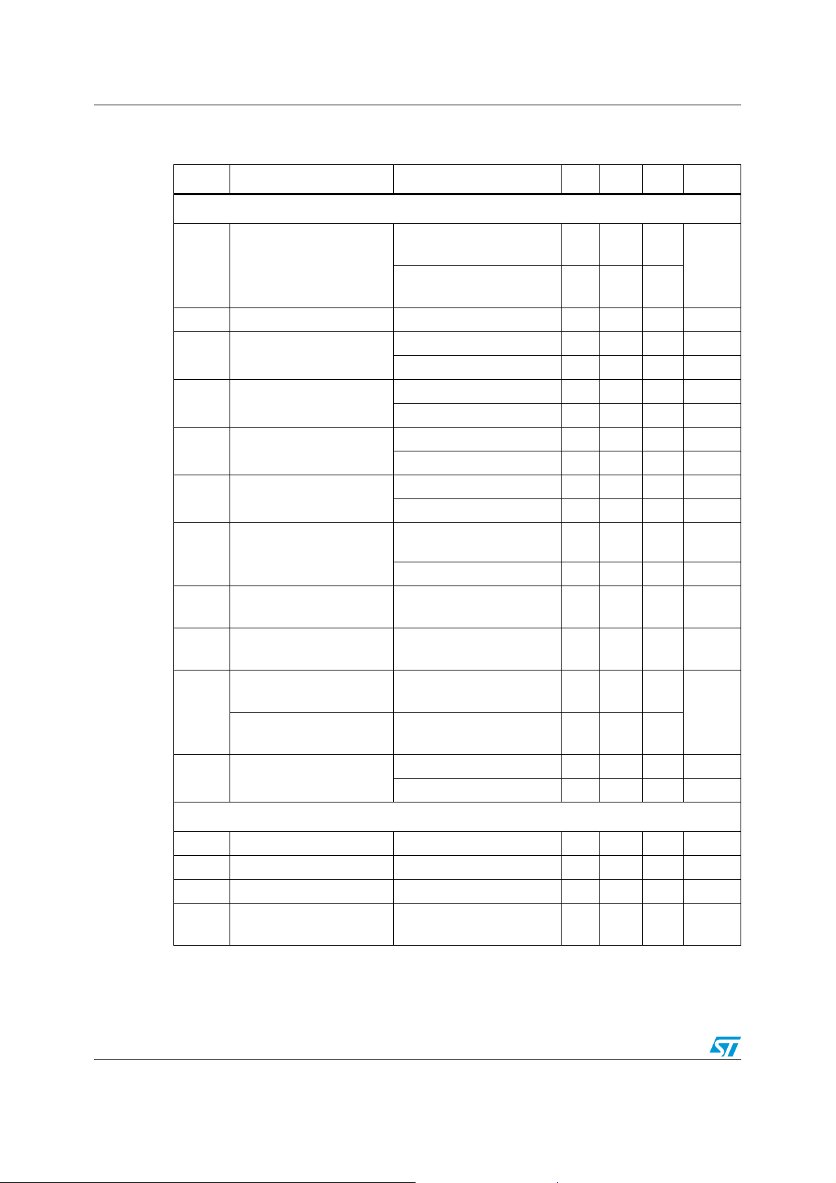
Electrical characteristics TSV611, TSV611A, TSV612, TSV612A
Table 5. V
= +5 V, V
CC+
= 0 V, V
CC-
= VCC/2, T
icm
= 25° C, RL connected to VCC/2
amb
(unless otherwise specified)
Symbol Parameter Min. Typ. Max. Unit
DC performance
V
Offset voltage
io
DV
CMR
SVR
V
V
Input offset voltage drift 2 μV/°C
io
I
Input offset current
io
I
Input bias current
ib
Common mode rejection
ratio 20 log (ΔV
Supply voltage rejection
ratio 20 log (ΔV
A
Large signal voltage gain
vd
High level output voltage
OH
Low level output voltage
OL
Isink
I
out
Isource
Supply current (per
I
CC
operator)
AC performance
/ΔVio)
ic
/ΔVio)
cc
TSV61x
TSV61xA
4
0.8
mV
T
min<Top<Tmax
T
min<Top<Tmax
< Top < T
T
min.
< Top < T
T
min.
0V to 5V, V
< Top < T
T
min.
TSV61x
TSV61xA
110
1 100 pA
max.
110
1 100 pA
max.
= 2.5 V 64 80 dB
out
63 dB
max.
5
2
(1)
pA
(1)
pA
Vcc = 1.8 to 5 V 76 93 dB
T
< Top < T
min.
=10kΩ, Vout = 0.5 V to
R
L
4.5 V
T
min<Top<Tmax
R
=10kΩ
L
T
< Top < T
min.
R
=10kΩ
L
T
< Top < T
min.
V
= V
o
CC
T
< Top < T
min.
= 0 V
V
o
< Top < T
T
min.
No load, V
T
min.
out=VCC
< Top < T
74 dB
max.
88 93 dB
85 dB
max.
35
50
7
16 35
max.
50
524257
max.
584963
max.
/2 7.5 10.5 14 µA
max.
715µA
mV
mV
mA
GBP Gain bandwidth product R
φm Phase margin R
Gain margin RL = 10 kΩ, CL=20pF 10 dB
G
m
SR Slew rate
=10kΩ, CL= 20 pF 120 kHz
L
= 10 kΩ, CL=20pF 62 Degrees
L
R
=10kΩ, CL= 20 pF,
L
V
= 0.5V to 4.5V
out
6/19 Doc ID 15768 Rev 2
0.04 V/μs
 Loading...