


查询TSV358IYD供应商
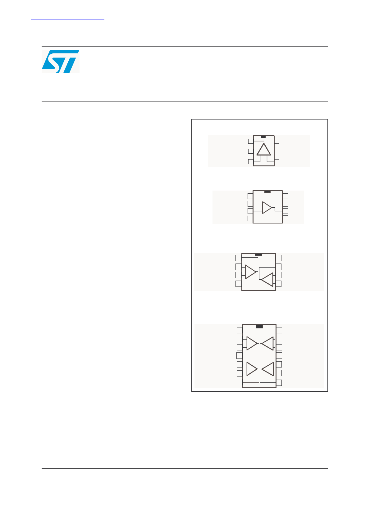
TSV321-TSV358-TSV324
General Purpose, Input/Output Rail-to-Rail
Low Power Operational Amplifiers
■ Operating at V
= 2.5V to 6V
CC
■ Rail-to-rail input & output
■ Extended V
(VDD - 0.2V to VCC + 0.2V)
icm
■ Capable of driving a 32Ω load resistor
■ High stability: 500pF
■ Available in SOT23-5 micropackage
■ Operating temperature range: -40, +125°C
Description
The TSV358 and TSV324 (dual & quad) are low
voltage versions of LM358 and LM324 commodity
operational amplifiers. TSV321 is the single
version. The TSV321/358/324 are able to operate
with voltage as low as 2.5V and features both I/O
rail-to-rail.
The common mode input voltage extends 200mV
at 25°C beyond the supply voltages while the
output voltage swing is within 100mV of each rail
with 600 Ohm load resistor. These devices offer
1.3MHz of gain-bandwidth product and provide
high output drive capability typically at 65mAload.
These performances make the TSV3xx family
ideal for active filters, general purpose low-voltage
applications, general purpose portable devices.
Applications
■ Battery-powered applications
■ Audio driver (headphone driver)
■ Sensor signal conditioning
■ Laptop/notebook computers
TSV321RILT
VCC
Output
Output
1
1
VDD
VDD
2
2
Non Inverting Input Inverting Input
Non Inverting Input Inverting Input
3
3
VCC
5
5
4
4
TSV321ID-TSV321IDT
N.C.
N.C.
Inverti ng Input
Inverti ng Input
Non Inver ting Input
Non Inver ting Input
VDD
VDD
1
1
_
_
2
2
+
+
3
3
8
N.C.
8
N.C.
VCC
VCC
7
7
Output
Output
6
6
N.C.
N.C.
54
54
TSV358IST-TSV358ID-TSV358IDT-TSV358IPT
Output 1
Output 1
Inverting Input 1
Inverting Input 1
Non Inverting Input 1
Non Inverting Input 1
VDD
VDD
1
1
_
_
2
2
+
+
3
3
VCC
VCC
8
8
7
7
Output 2
Output 2
_
_
Inverting Input 2
Inverting Input 2
6
6
+
+
Non Inverting Input 2
Non Inverting Input 2
54
54
TSV324ID-TSV324IDT-TSV324IPT
Output 4
Output 1
Output 1
Inverting Input 1
Inverting Input 1
Non Inverting Input 1
Non Inverting Input 1
VCC
VCC
Non Inverting Input 2
Non Inverting Input 2
Inverting Input 2
Inverting Input 2
Output 2
Output 2
1
1
_
_
2
2
+
+
3
3
4
4
5
5
+
+
_
_
6
6
7
7
Output 4
14
14
_
_
13
13
Inverting Input 4
Inverting Input 4
+
+
Non Inverting Input 4
Non Inverting Input 4
12
12
VDD
VDD
11
11
10
10
Non Inverting Input 3
Non Inverting Input 3
+
+
_
_
Inverting Input 3
Inverting Input 3
9
9
Output 3
Output 3
8
8
December 2005 Rev. 3 1/15
www.st.com
15
Order Codes TSV321-TSV358-TSV324
1 Order Codes
Part Number
TSV321RILT
TSV321RAILT SOT23-5L Tape & Reel K178
TSV321ID/IDT
TSV358ID/IDT V358ID
TSV358IPT
TSV358IST MiniSO-8 K175
TSV358IYD/IYDT SO-8 (automotive grade level) Tube or Tape & Reel
TSV358IYPT
TSV324ID/IDT SO-14 Tube or Tape & Reel V324ID
TSV324IPT
Temperature
Range
-40°C to +125°C
Package Packaging Marking
SOT23-5L Tape & Reel K174
SO-8 Tube or Tape & Reel
TSSOP8
(Thin Shrink Outline Package)
TSSOP8
(automotive grade level)
TSSOP14
(Thin Shrink Outline Package)
V321ID
V358I
Tape & Reel
Tape & Reel V358Y
Tape & Reel V324IP
2/15
TSV321-TSV358-TSV324 Absolute Maximum Ratings
2 Absolute Maximum Ratings
Table 1. Key parameters and their absolute maximum ratings
Symbol Parameter Value Unit
V
CC
V
id
V
T
stg
T
R
thja
ESD
Supply Voltage
Differential Input Voltage
Input Voltage VDD-0.3 to VCC +0.3
i
(1)
(2)
Storage Temperature
Maximum Junction Temperature
j
Thermal Resistance Junction to Ambient
(3)
SOT23-5
SO-8
SO-14
TSSOP8
TSSOP14
MiniSO-8
HBM: Human Body Model
MM: Machine Model
(4)
(5)
7V
±1 V
-65 to +150 °C
150 °C
250
125
103
120
100
190
2kV
200 V
CDM: Charged Device Model 1.5 kV
Latch-up Immunity 200 mA
Lead Temperature (soldering, 10s) 250 °C
Output Short Circuit Duration
see note
(6)
V
°C/W
1. All voltages values, except differential voltage are with respect to network terminal.
2. Differential voltages are the non-inverting input terminal with respect to the inverting input terminal. If Vid > ±1V, the
maximum input current must not exceed ±1mA. In this case (Vid > ±1V) an input series resistor must be added to limit input
current.
3. Short-circuits can cause excessive heating. Destructive dissipation can result from simultaneous short-circuit on all
amplifiers.
4. Human body model, 100pF discharged through a 1.5kΩ resistor into pin of device.
5. Machine model ESD, a 200pF cap is charged to the specified voltage, then discharged directly into the IC with no external
series resistor (internal resistor < 5Ω), into pin to pin of device.
6. Short-circuits from the output to VCCcan cause excessive heating. The maximum output current is approximately 80mA,
independent of the magnitude of V
. Destructive dissipation can result from simultaneous short-circuits on all amplifiers.
CC
Table 2. Operating conditions
Symbol Parameter Value Unit
V
V
V
T
1. At 25°C, for 2.5 ≤ VCC ≤ 6V, V
2. In full temperature range, both Rails can be reached when VCC does not exceed 5.5V.
Supply Voltage 2.5 to 6 V
CC
Common Mode Input Voltage Range
icm
Common Mode Input Voltage Range
icm
Operating Free Air Temperature Range -40 to + 125 °C
oper
is extended to VDD - 0.2V, VCC + 0.2V.
icm
(1)
(2)
VDD - 0.2 to VCC + 0.2 V
VDD to V
3/15
CC
V
Electrical Characteristics TSV321-TSV358-TSV324
3 Electrical Characteristics
Table 3. V
= +3V, VDD = 0V, RL, CL connected to VCC/2, T
CC
= 25°C (unless otherwise specified)
amb
Symbol Parameter Conditions Min. Typ. Max. Unit
= V
= V
V
Input Offset Voltage
V
io
icm
TSV321/358/324
TSV321A/358A/324A
∆V
Input Offset Voltage Drift 2 µV/°C
io
I
Input Offset Current
io
Input Bias Current
I
ib
(1)
1)
V
icm
V
icm
CMR Common Mode Rejection Ratio 0 ≤ V
= V
= V
icm
out
= V
out
= V
out
≤ VCC, V
/2
CC
0.2
0.1
/2 3 30 nA
CC
/2 4 125 nA
CC
= V
out
/2 60 80 dB
CC
3
1
mV
SVR Supply Voltage Rejection Ratio 70 85 dB
V
= 0.5V to 2.5V
Large Signal Voltage Gain
A
vd
V
V
High Level Output Voltage
OH
Low Level Output Voltage
OL
Output Source Current VID = 100mV, VO = V
I
o
Output Sink Current V
I
Supply Current (per amplifier) A
CC
GBP Gain Bandwidth Product R
SR Slew Rate R
φm Phase Margin C
out
= 2kΩ
R
L
R
= 600Ω
L
= 100mV
V
id
= 2kΩ
R
L
R
= 600Ω
L
= -100mV
V
id
= 2kΩ
R
L
R
= 600Ω
L
DD
= -100mV, VO = V
ID
= 1, no load 420 650 µA
VCL
= 10kΩ, CL= 100pF, f = 100kHz 1 1.3 MHz
L
= 10kΩ, CL= 100pF, AV = 1 0.42 0.6 V/µs
L
= 100pF 53 Degrees
L
CC
80
74
2.82
2.80
20 80
20 80
92
95
2.95
2.95
88
115
120
160
dB
mV
mA
en Input Voltage Noise 27 nV/√Hz
V
THD Total Harmonic Distortion 0.01 %
1. Maximum values including unavoidable inaccuracies of the industrial test.
4/15
TSV321-TSV358-TSV324 Electrical Characteristics
Table 4. VCC = +5V, VDD = 0V, RL, CL connected to VCC/2, T
= 25°C (unless otherwise specified)
amb
Symbol Parameter Conditions Min. Typ. Max. Unit
= V
= V
V
Input Offset Voltage
V
io
icm
TSV321/358/324
TSV321A/358A/324A
∆V
Input Offset Voltage Drift 2 µV/°C
io
I
Input Offset Current
io
I
Input Bias Current
ib
(1)
1)
V
icm
V
icm
CMR Common Mode Rejection Ratio 0 ≤ V
= V
= V
icm
out
= V
out
= V
out
≤ VCC, V
/2
CC
0.2
0.1
/2 3 30 nA
CC
/2 70 130 nA
CC
= V
out
/2 65 85 dB
CC
3
1
mV
SVR Supply Voltage Rejection Ratio 70 90 dB
V
= 0.5V to 2.5V
Large Signal Voltage Gain
A
vd
V
V
High Level Output Voltage
OH
Low Level Output Voltage
OL
Output Source Current VID = 100mV, VO = V
I
o
Output Sink Current V
Supply Current (per amplifier) A
I
CC
GBP Gain Bandwidth Product R
SR Slew Rate R
φm Phase Margin C
out
= 2kΩ
R
L
R
= 600Ω
L
= 100mV
V
id
= 2kΩ
R
L
R
= 600Ω
L
V
= -100mV
id
= 2kΩ
R
L
R
= 600Ω
L
DD
= -100mV, VO = V
ID
= 1, no load 500 835 µA
VCL
= 10kΩ, CL= 100pF, f = 100kHz 1 1.4 MHz
L
= 10kΩ, CL= 100pF, AV = 1 0.42 0.6 V/µs
L
= 100pF 55 Degrees
L
CC
83
77
4.80
4.75
20 80
20 80
92
85
4.95
4.90
88
115
130
188
dB
mV
mA
en Input Voltage Noise 27 nV/√Hz
V
THD Total Harmonic Distortion 0.01 %
1. Maximum values including unavoidable inaccuracies of the industrial test.
5/15