

TSV321-TSV358-TSV324
General purpose input/output rail-to-rail
low power operational amplifiers
Features
■ Operating range V
■ Rail-to-rail input and output
■ Extended V
icm
■ Capable of driving a 32 Ω load resistor
■ High stability: 500 pF
■ Available in SOT23-5 micropackage
■ Operating temperature range: -40° C, +125° C
= 2.5 V to 6 V
CC
(VDD - 0.2 V to VCC + 0.2 V)
Applications
■ Battery-powered applications
■ Audio driver (headphone driver)
■ Sensor signal conditioning
■ Laptop/notebook computers
Description
The TSV358 and TSV324 (dual and quad) are
low voltage versions of the LM358 and LM324
commodity operational amplifiers . The TSV321 is
the single version. The TSV321/358/324 are able
to operate with voltages as low as 2.5 V and
feature both I/O rail-to-rail.
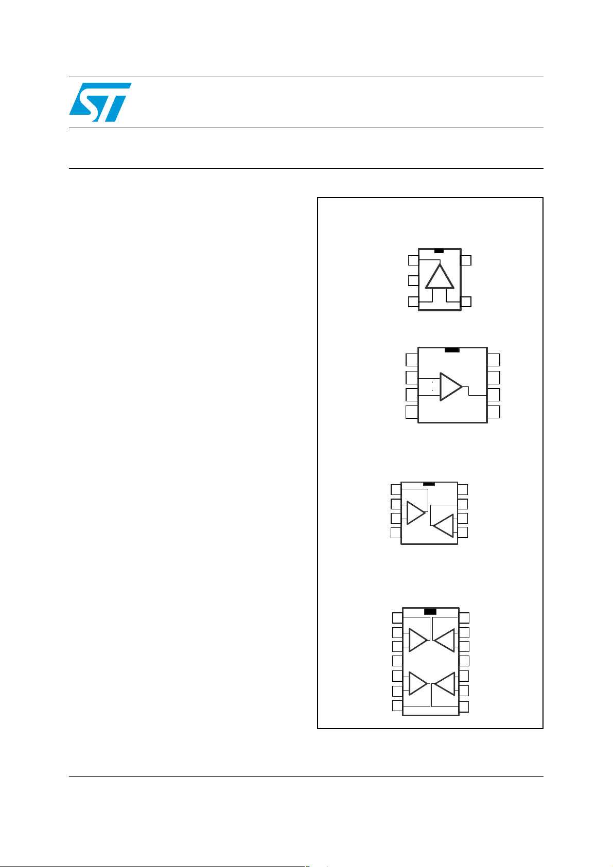
Pin connections (top view)
TSV321RILT (SOT23-5)
VCC
Output
Output
Non Inverting Input Inverting Input
Non Inverting Input Inverting Input
VDD
VDD
1
1
2
2
3
3
VCC
5
5
4
4
TSV321ID-TSV321IDT (SO-8)
N.C.
N.C.
Inverting Input
Inverting Input
Non Inverting Input
Non Inverting Input
VDD
VDD
1
1
_
2
2
3
3
4
4
_
+
+
8
N.C.
8
N.C.
VCC
VCC
7
7
Output
Output
6
6
N.C.
N.C.
5
5
TSV358IST-TSV358ID-TSV358IDT-TSV358IPT
(SO-8, miniSO-8, TSSOP8)
Output 1
Output 1
Inverting Input 1
Inverting Input 1
Non Inverting Input 1
Non Inverting Input 1
VDD
VDD
1
1
_
_
2
2
+
+
3
3
4
4
VCC
VCC
8
8
7
7
Output 2
Output 2
_
_
Inverting Input 2
Inverting Input 2
6
6
+
+
Non Inverting Input 2
Non Inverting Input 2
5
5
The common mode input voltage e xtends 200 mV
beyond the supply voltages at 25° C while the
output voltage swing is within 100 mV of each rail
with a 600 Ω load resistor. At V
= 3 V, these
CC
TSV324ID-TSV324IDT-TSV324IPT
(SO-14, TSSOP14)
devices offer 1.3 MHz of gain-bandwidth product
and provide high output current capability with a
typical value of 80 mA.
These features make the TSV3xx family ideal for
active filters, general purpose low-voltage
applications, and general purpose portable
devices.
Output 1
Output 1
Inverting Input 1
Inverting Input 1
Non Inverting Input 1
Non Inverting Input 1
Non Inverting Input 2
Non Inverting Input 2
Inverting Input 2
Inverting Input 2
Output 2
Output 2
VCC
VCC
1
1
_
_
2
2
+
+
3
3
4
4
5
5
+
+
_
_
6
6
7
7
February 2008 Rev 5 1/17
Output 4
Output 4
14
14
_
_
13
13
Inverting Input 4
Inverting Input 4
+
+
Non Inverting Input 4
Non Inverting Input 4
12
12
VDD
VDD
11
11
10
10
Non Inverting Input 3
Non Inverting Input 3
+
+
_
_
Inverting Input 3
Inverting Input 3
9
9
Output 3
Output 3
8
8
www.st.com
17

Absolute maximum ratings and operating conditions TSV321-TSV358-TSV324
1 Absolute maximum ratings and operating conditions
Table 1. Absolute maximum ratings
Symbol Parameter Value Unit
V
CC
V
id
V
in
T
stg
T
R
thja
R
thjc
ESD
Supply voltage
Differential input voltage
Input voltage VDD-0.3 to VCC +0.3 V
Storage temperature -65 to +150 °C
Maximum junction temperature 150 °C
j
Thermal resistance junction to ambient
SOT23-5
SO-8
SO-14
TSSOP8
TSSOP14
MiniSO-8
Thermal resistance junction to case
SOT23-5
SO-8
SO-14
TSSOP8
TSSOP14
MiniSO-8
HBM: human body model
MM: machine model
CDM: charged device model
(1)
(5)
(2)
(4)
(6)
(3)
(3)
7V
±1 V
250
°C/W
125
105
120
100
190
81
°C/W
40
31
37
32
39
2kV
200 V
1.5 kV
Latch-up immunity 200 mA
Lead temperature (soldering, 10s) 250 °C
Output short-circuit duration See note
1. All voltages values, except differential voltage are with respect to network terminal.
2. Differential voltages are the non-inverting input terminal with respect to the inverting input terminal. If
V
> ±1 V, the maximum input current must not exceed ±1 mA. When Vid > ±1 V, an input series resistor
id
must be added to limit input current.
3. Short-circuits can cause excessive heating and destructive dissipation. Rth are typical values.
4. Human body model: 100pF discharged through a 1.5 kΩ resistor between two pins of the device, done for
all couples of pin combinations with other pins floating.
5. Machine model: a 200pF capacitor is charged to the specified voltage, then discharged directly between
two pins of the device with no external series resistor (internal resistor < 5
combinations with other pins floating.
6. Charged device model: all pins plus package are charged together to the specified voltage and then
discharged directly to the ground.
7. Short-circuits from the output to VCCcan cause excessive heating. The maximum output current is
approximately 80 mA, independent of the magnitude of V
simultaneous short-circuits on all amplifiers.
2/17
(7)
Ω), done for all couples of pin
. Destructive dissipation can result from
CC

TSV321-TSV358-TSV324 Absolute maximum ratings and operating conditions
Table 2. Operating conditions
Symbol Parameter Value Unit
V
V
T
Supply voltage 2.5 to 6 V
CC
Common mode input voltage range
V
= 25°C, 2.5 ≤ VCC ≤ 6V
icm
oper
T
amb
T
< T
< T
min
amb
, 2.5 ≤ VCC ≤ 5.5V
max
Operating free air temperature range -40 to + 125 °C
- 0.2 to VCC + 0.2
DD
VDD to V
V
CC
3/17

Electrical characteristics TSV321-TSV358-TSV324
2 Electrical characteristics
Table 3. Electrical characteristics at VCC = +3V, VDD = 0V, RL, CL connected to VCC/2,
and T
= 25°C (unless otherwise specified)
amb
Symbol Parameter Test conditions Min. Typ. Max. Unit
V
= V
= V
V
Input offset voltage
io
icm
out
TSV321/358/324
≤ T
T
min
amb
TSV321A/358A/324A
T
≤ T
min
amb
≤ T
≤ T
CC
max
max
/2
0.2
0.1
3
6
mV
1
3
ΔVioInput offset voltage drift 2 µV/°C
Input offset current
I
io
I
Input bias current
ib
CMR
V
V
Common mode rejection ratio
20 log (ΔVic/ΔVio)
A
Large signal voltage gain
vd
High level output voltage
OH
Low level output voltage
OL
Output source current Vid = 100mV, VO = V
I
o
Output sink current V
I
Supply current (per amplifier)
CC
GBP Gain bandwidth product R
SR Slew rate R
φm Phase margin C
V
= V
icm
T
min
V
icm
T
min
0 ≤ V
V
out
R
= V
out
≤ T
≤ T
amb
= V
= V
out
≤ T
≤ T
amb
≤ VCC, V
icm
= 0.5V to 2.5V
= 2kΩ
L
RL = 600Ω
V
= 100mV
id
= 2kΩ
R
L
RL = 600Ω
T
≤ T
min
T
V
id
R
amb
≤ T
min
amb
= -100mV
= 2kΩ
L
RL = 600Ω
T
≤ T
min
amb
≤ T
min
amb
= -100mV, VO = V
= 1, no load
≤ T
≤ T
amb
=10kΩ, CL= 100pF, f = 100kHz 1 1.3 MHz
=10kΩ, CL= 100pF 0.42 0.6 V/µs
= 100pF 53 Degrees
A
T
T
id
VCL
min
L
L
L
CC
max
CC
max
≤ T
≤ T
≤ T
≤ T
max
(1)
/2
(1)
/2
= V
out
max, RL
max, RL
max, RL
max, RL
DD
330
40 125
150
/2 60 80 dB
CC
= 2kΩ
= 600Ω
= 2kΩ
= 600Ω
80
74
2.82
2.80
2.82
2.80
92
95
2.95
2.95
88
115
120
160
120
160
20 80
CC
20 80
420 650
690
60
nA
nA
dB
mV
mA
µA
en Input voltage noise 27 nV/√Hz
THD Total harmonic distortion 0.01 %
1. Maximum values include unavoidable inaccuracies of the industrial tests.
V
4/17
TSV321-TSV358-TSV324 Electrical characteristics
T ab le 4. Electrical characteristics at VCC = +5V, VDD = 0V, RL, CL connected to VCC/2,
and T
= 25°C (unless otherwise specified)
amb
Symbol Parameter Conditions Min. Typ. Max. Unit
V
= V
= V
V
Input offset voltage
io
icm
out
TSV321/358/324
≤ T
T
min
amb
TSV321A/358A/324A
≤ T
T
min
amb
≤ T
≤ T
CC
max
max
/2
0.2
0.1
3
6
mV
1
3
ΔVioInput offset voltage drift 2 µV/°C
I
Input offset current
io
I
Input bias current
ib
CMR
SVR
V
V
Common mode rejection ratio
20 log (ΔVic/ΔVio)
Supply voltage rejection ratio
20 log (ΔV
Large signal voltage gain
A
vd
High level output voltage
OH
Low level output voltage
OL
CC
/ΔVio)
Output source current Vid = 100mV, VO = V
I
o
Output sink current V
Supply current (per amplifier)
I
CC
GBP Gain bandwidth product R
SR Slew rate R
φm Phase margin C
V
= V
≤ T
= V
≤ T
icm
= V
out
≤ T
amb
= V
out
≤ T
amb
≤ VCC, V
icm
T
min
V
icm
T
min
0 ≤ V
VCC = 2.5 to 5V 70 90 dB
= 0.5V to 4.5V
V
out
RL = 2kΩ
= 600Ω
R
L
V
= 100mV
id
RL = 2kΩ
= 600Ω
R
L
T
≤ T
min
T
V
id
R
amb
≤ T
min
amb
= -100mV
= 2kΩ
L
RL = 600Ω
T
≤ T
min
amb
≤ T
min
amb
= -100mV, VO = V
= 1, no load
≤ T
≤ T
amb
=10kΩ, CL= 100pF, f = 100kHz 1 1.4 MHz
=10kΩ, CL= 100pF 0.42 0.6 V/µs
= 100pF 55 Degrees
A
T
T
id
VCL
min
L
L
L
CC
max
CC
max
≤ T
≤ T
≤ T
≤ T
max
(1)
/2
(1)
/2
= V
out
max, RL
max, RL
max, RL
max, RL
DD
330
70 130
150
/2 65 85 dB
CC
= 2kΩ
= 600Ω
= 2kΩ
= 600Ω
83
77
4.80
4.75
4.80
4.75
92
85
4.95
4.90
88
115
130
188
130
188
20 80
CC
20 80
500 835
875
60
nA
nA
dB
mV
mA
µA
en Input voltage noise 27 nV/√Hz
THD Total harmonic distortion 0.01 %
V
1. Maximum values include unavoidable inaccuracies of the industrial tests.
5/17

Electrical characteristics TSV321-TSV358-TSV324
Figure 1. Supply current/amplifier vs. supply
600
600
500
500
400
400
300
300
200
200
Supply Current (µA)
Supply Current (µA)
100
100
0
0
Figure 2. Supply current/amplifier vs.
voltage
550
550
500
500
450
450
Tamb = 25°C
Tamb = 25°C
02468
02468
Supply Voltage (V)
Supply Voltage (V)
400
400
350
350
Supply Current (µA)
Supply Current (µA)
300
300
250
250
temperature
Vcc = 5V
Vcc = 5V
Vcc = 3V
Vcc = 3V
-40-200 20406080100120140
-40-200 20406080100120140
Temperature (°C)
Temperature (°C)
Figure 3. Output power vs. supply voltage Figure 4. Input offset voltage drift vs.
temperature
200
60
60
RL = 32 ohms
RL = 32 ohms
50
50
40
40
30
30
20
20
Output Power ( mW)
Output Power ( mW)
10
10
0
0
123456
123456
10% distortion
10% distortion
0.1% distortion
0.1% distortion
Supply Voltage (V)
Supply Voltage (V)
1% distorti o n
1% distorti o n
200
150
150
100
100
50
50
0
0
-50
-50
Input Voltage Drift (µV)
Input Voltage Drift (µV)
-100
-100
-150
-150
-40-200 20406080100120140
-40-200 20406080100120140
Temperature (°C)
Temperature (°C)
Vcc = 3V
Vcc = 3V
Vcc = 5V
Vcc = 5V
Figure 5. Input bias current vs. temperature Figure 6. Open loop gain vs. temperature at
V
=5V
CC
110
10.0
10.0
0.0
0.0
-10.0
-10.0
-20.0
-20.0
Input bias current (nA)
Input bias current (nA)
-30.0
-30.0
-40.0
-40.0
-40 -20 0 20 40 60 80 100 120 140
-40 -20 0 20 40 60 80 100 120 140
Temperature (°C)
Temperature (°C)
Vcc = 3V
Vcc = 3V
Vicm = 1.5V
Vicm = 1.5V
6/17
110
Vcc = 5V
Vcc = 5V
Vicm = 2.5V
Vicm = 2.5V
100
100
90
90
80
80
Open Loop Gain (dB)
Open Loop Gain (dB)
70
70
-40-200 20406080100120140
-40-200 20406080100120140
Temperature (°C)
Temperature (°C)
RL = 2 kOhms
RL = 2 kOhms
RL = 600 ohms
RL = 600 ohms

TSV321-TSV358-TSV324 Electrical characteristics
Figure 7. Open loop gain vs. temperature at
V
=3V
CC
110
110
Vcc = 3V
Vcc = 3V
Vicm = 1.5V
Vicm = 1.5V
100
100
90
90
80
80
Open Loop Gain (dB)
Open Loop Gain (dB)
70
70
-40-200 20406080100120140
-40-200 20406080100120140
Temperature (°C)
Temperature (°C)
RL = 2 kOhms
RL = 2 kOhms
RL = 600 Ohms
RL = 600 Ohms
Figure 9. Low level output voltage vs.
temperature
110
110
RL = 600 ohms
RL = 600 ohms
100
100
90
90
80
80
70
70
Vcc = 5V
Vcc = 5V
Vcc = 3V
Vcc = 3V
Figure 8. High level output voltage vs.
temperature
110
110
RL = 600 ohms
RL = 600 ohms
100
100
90
90
80
80
70
70
60
60
50
50
Voltage Referenced to VCC (mV)
Voltage Referenced to VCC (mV)
40
40
-40-20 0 20 40 60 80100120140
-40-20 0 20 40 60 80100120140
Vcc = 5V
Vcc = 5V
Vcc = 3V
Vcc = 3V
Temperature (°C)
Temperature (°C)
Figure 10. Output current vs. temperature at
V
=5V
CC
100
100
Isink
50
50
0
0
Isink
Vcc = 5V
Vcc = 5V
Vid = 1V
Vid = 1V
60
60
50
50
Voltage Referenced to Gnd (mV)
Voltage Referenced to Gnd (mV)
40
40
-40-20 0 20 40 60 80100120140
-40-20 0 20 40 60 80100120140
Temperature (°C)
Temperature (°C)
Figure 11. Output current vs. temperature at
V
=3V
CC
100
100
Isink
Isink
50
50
Vcc = 3V
Vcc = 3V
Vid = 1V
0
0
Output Current (mA)
Output Current (mA)
-50
-50
-100
-100
-40 -20 0 20 40 60 80 100 120 140
-40 -20 0 20 40 60 80 100 120 140
Vid = 1V
Isource
Isource
Temperature (°C)
Temperature (°C)
Isource
Output Current (mA)
Output Current (mA)
-50
-50
-100
-100
-40-200 20406080100120140
-40-200 20406080100120140
Isource
Temperature (°C)
Temperature (°C)
Figure 12. Output current vs. output v oltage at
VCC=5V
100
100
50
50
0
0
T = 125 °C
T = 125 °C
Output Current (mA)
Output Current (mA)
-100
-100
T = 25 °C
T = 25 °C
-50
-50
T = -40 °C
T = -40 °C
0.0 1.0 2.0 3.0 4.0 5.0
0.0 1.0 2.0 3.0 4.0 5.0
T = 125 °C
T = 125 °C
T = -40 °C
T = -40 °C
Vcc = 5V
Vcc = 5V
Vid = 0.1V
Vid = 0.1V
Vicm = 2.5V
Vicm = 2.5V
Output Voltage (V)
Output Voltage (V)
sink
sink
T = 25 °C
T = 25 °C
source
source
7/17

Electrical characteristics TSV321-TSV358-TSV324
Figure 13. Output current vs. output v oltage at
V
=3V
CC
100
100
50
50
0
0
T = 125 °C
T = 125 °C
Output Current (mA)
Output Current (mA)
-100
-100
T = 25 °C
T = 25 °C
-50
-50
T = -40 °C
T = -40 °C
0.0 0.5 1.0 1.5 2.0 2.5 3.0 3.5
0.0 0.5 1.0 1.5 2.0 2.5 3.0 3.5
v
T = 125 °C
T = 125 °C
T = -40 °C
T = -40 °C
Vcc = 3V
Vcc = 3V
Vid = 0.1V
Vid = 0.1V
Vicm = 1.5V
Vicm = 1.5V
Output Voltage (V)
Output Voltage (V)
sink
sink
T = 25 °C
T = 25 °C
source
source
Figure 15. Gain and phase vs. frequency at
V
=3V
CC
70
70
RL = 10K
60
60
50
50
40
40
gain
gain
30
30
Gain (dB)
Gain (dB)
20
20
10
10
0
0
1E+3 1E+4 1E+5 1E+6
1E+3 1E+4 1E+5 1E+6
Frequency (Hz)
Frequency (Hz)
RL = 10K
CL = 100 pF
CL = 100 pF
Vcc = 3V
Vcc = 3V
phase
phase
180
180
160
160
140
140
120
120
100
100
80
80
60
60
40
40
Phase (°)
Phase (°)
Figure 14. Gain and phase vs. frequency at
VCC=5V
70
70
RL = 10K
60
60
50
50
40
40
gain
gain
30
30
Gain (dB)
Gain (dB)
20
20
10
10
0
0
1E+3 1E+4 1E+5 1E+6
1E+3 1E+4 1E+5 1E+6
Frequency (Hz)
Frequency (Hz)
RL = 10K
CL = 100 pF
CL = 100 pF
Vcc = 5V
Vcc = 5V
phase
phase
180
180
160
160
140
140
120
120
100
100
80
80
60
60
40
40
Figure 16. Slew rate vs. temperature at
VCC=5V
0.75
0.75
Vcc = 5V
Vcc = 5V
gain = +1
gain = +1
0.70
0.70
Vin = 2 to 3V
Vin = 2 to 3V
0.65
0.65
RL = 10kohms
RL = 10kohms
CL = 100 pF
CL = 100 pF
0.60
0.60
0.55
0.55
0.50
0.50
Slew Rate (V/µs)
Slew Rate (V/µs)
0.45
0.45
0.40
0.40
0.35
0.35
-40-200 20406080100120140
-40-200 20406080100120140
positive Slew Rate
positive Slew Rate
negative Slew Rate
negative Slew Rate
Temperature (°C)
Temperature (°C)
Phase (° )
Phase (° )
Figure 17. Slew rate vs. temperature at
V
=3V
CC
0.70
0.70
Vcc = 3V
Vcc = 3V
gain = +1
gain = +1
0.65
0.65
Vin = 1 to 2V
Vin = 1 to 2V
RL = 10kohm
RL = 10kohm
0.60
0.60
CL = 100 pF
CL = 100 pF
0.55
0.55
0.50
0.50
Slew Rate (V/µs )
Slew Rate (V/µs )
0.45
0.45
0.40
0.40
0.35
0.35
-40-200 20406080100120140
-40-200 20406080100120140
Temperature (°C)
Temperature (°C)
8/17
positive Slew Rate
positive Slew Rate
negative Slew Rate
negative Slew Rate
Figure 18. Distortion vs. frequency
0.150
Distortion (%)
Distortion (%)
0.150
0.125
0.125
0.100
0.100
0.075
0.075
0.050
0.050
0.025
0.025
0.000
0.000
Vcc = 3V
Vcc = 3V
Vout = 1Vpp
Vout = 1Vpp
RL = 32 ohms
RL = 32 ohms
gain = -1
gain = -1
1E+1 1E+2 1E+3 1E+4 1E+5
1E+1 1E+2 1E+3 1E+4 1E+5
Frequency (Hz)
Frequency (Hz)

TSV321-TSV358-TSV324 Package information
3 Package information
In order to meet environmental requirements, STMicroelectronics offers these devices in
ECOPACK
®
packages. These packages have a lead-free second level interconnect. The
category of second level interconnect is marke d on the pa ckage and on the inner box label,
in compliance with JEDEC Standard JESD97. The maximum ratings related t o soldering
conditions are also marked on the inner box label. ECOPACK is an STMicroelectronics
trademark. ECOPACK specifications are available at: www.st.com
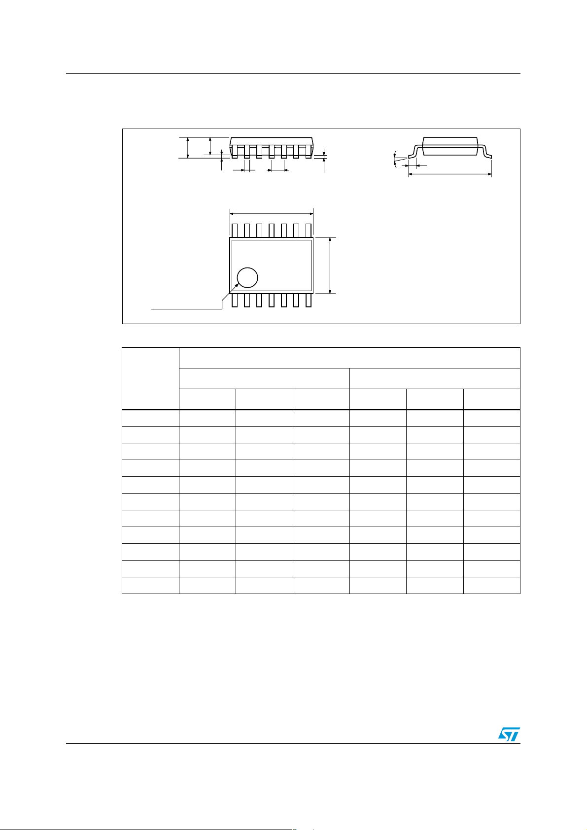
3.1 SOT23-5 package information
Figure 19. SOT23-5 package mechanical drawing
.
Table 5. SOT23-5 package mechanical data
Dimensions
Ref.
Min. Typ. Max. Min. Typ. Max.
A 0.90 1.45 35.4 57.1
A1 0.00 0.15 0.00 5.9
A2 0.90 1.30 35.4 51.2
b 0.35 0.50 13.7 19.7
C 0.09 0.20 3.5 7.8
D 2.80 3.00 110.2 118.1
E 2.60 3.00 102.3 118.1
E1 1.50 1.75 59.0 68.8
e 0.95 37.4
e1 1.9 74.8
L 0.35 0.55 13.7 21.6
Millimeters Mils
9/17

Package information TSV321-TSV358-TSV324
3.2 SO-8 package information
Figure 20. SO-8 package mechanical drawing
Table 6. SO-8 package mechanical data
Dimensions
Ref.
Min. Typ. Max. Min. Typ. Max.
A1.750.069
A1 0.10 0.25 0.004 0.010
A2 1.25 0.049
b 0.28 0.48 0.011 0.019
c 0.17 0.23 0.007 0.010
D 4.80 4.90 5.00 0.189 0.193 0.197
E 5.80 6.00 6.20 0.228 0.236 0.244
E1 3.80 3.90 4.00 0.150 0.154 0.157
e 1.27 0.050
h 0.25 0.50 0.010 0.020
L 0.40 1.27 0.016 0.050
k1°8°1°8°
ccc 0.10 0.004
Millimeters Inches
10/17

TSV321-TSV358-TSV324 Package information
3.3 TSSOP8 package information
Figure 21. TSSOP8 package mechanical drawing
Table 7. TSSOP8 package mechanical data
Dimensions
Ref.
Min. Typ. Max. Min. Typ. Max.
A 1.2 0.047
A1 0.05 0.15 0.002 0.006
A2 0.80 1.00 1.05 0.031 0.039 0.041
b 0.19 0.30 0.007 0.012
c 0.09 0.20 0.004 0.008
D 2.90 3.00 3.10 0.114 0.118 0.122
E 6.20 6.40 6.60 0.244 0.252 0.260
E1 4.30 4.40 4.50 0.169 0.173 0.177
e 0.65 0.0256
k0°8°0°8°
L 0.45 0.60 0.75 0.018 0.024 0.030
L1 1 0.039
aaa 0.1 0.004
Millimeters Inches
11/17

Package information TSV321-TSV358-TSV324
3.4 MiniSO-8 package information
Figure 22. MiniSO-8 package mechanical drawing
Table 8. MiniSO-8 package mechanical data
Dimensions
Ref.
Min. Typ. Max. Min. Typ. Max.
A 1.1 0.043
A1 0 0.15 0 0.006
A2 0.75 0.85 0.95 0.030 0.033 0.037
b 0.22 0.40 0.009 0.016
c 0.08 0.23 0.003 0.009
D 2.80 3.00 3.20 0.11 0.118 0.126
E 4.65 4.90 5.15 0.183 0.193 0.203
E1 2.80 3.00 3.10 0.11 0.118 0.122
e 0.65 0.026
L 0.40 0.60 0.80 0.016 0.024 0.031
L1 0.95 0.037
L2 0.25 0.010
k0°8°0°8°
ccc 0.10 0.004
Millimeters Inches
12/17

TSV321-TSV358-TSV324 Package information
3.5 SO-14 package information
Figure 23. SO-14 package mechanical drawing
Table 9. SO-14 package mechanical data
Dimensions
Ref.
Min. Typ. Max. Min. Typ. Max.
A1.750.068
a1 0.1 0.2 0.003 0.007
a2 1.65 0.064
b 0.35 0.46 0.013 0.018
b1 0.19 0.25 0.007 0.010
C0.5 0.019
c1 45° (typ.)
D 8.55 8.75 0.336 0.344
E 5.8 6.2 0.228 0.244
e 1.27 0.050
e3 7.62 0.300
F 3.8 4.0 0.149 0.157
G 4.6 5.3 0.181 0.208
Millimeters Inches
L 0.5 1.27 0.019 0.050
M0.680.026
S 8° (max.)
13/17
Package information TSV321-TSV358-TSV324
3.6 TSSOP14 package information
Figure 24. TSSOP14 package mechanical drawing
A2
A
A1
b
e
D
c
E1
K
L
E
PIN 1 IDENTIFICATION
1
Figure 25. TSSOP14 package mechanical data
Dimensions
Ref.
Min. Typ. Max. Min. Typ. Max.
A 1.2 0.047
A1 0.05 0.15 0.002 0.004 0.006
A2 0.8 1 1.05 0.031 0.039 0.041
b 0.19 0.30 0.007 0.012
c 0.09 0.20 0.004 0.0089
D 4.9 5 5.1 0.193 0.197 0.201
E 6.2 6.4 6.6 0.244 0.252 0.260
E1 4.3 4.4 4.48 0.169 0.173 0.176
e 0.65 BSC 0.0256 BSC
K0°8°0°8°
L1 0.45 0.60 0.75 0.018 0.024 0.030
Millimeters Inches
14/17

TSV321-TSV358-TSV324 Ordering information
4 Ordering information
Table 10. Order codes
TSV321RILT
Order code
Temperature
range
Package Packaging Marking
K174
SOT23-5 Tape & reel
TSV321RAILT K178
(1)
(1)
(1)
(1)
(1)
(1)
(1)
-40°C to +125°C
SOT23-5
(Automotive grade level)
SO-8
(Automotive grade level)
SO-8
SO-8
(Automotive grade level)
TSSOP8
(Thin shrink outline package)
TSSOP8
(Automotive grade level)
Tape & reel
Tube or
tape & reel
Tube or
tape & reel
Tube or
tape & reel
Tube or
tape & reel
Tube or
tape & reel
Tape & reel
Tape & reel
TSV321RIYLT
TSV321RAIYLT
TSV321ID/IDT SO-8
TSV321IYD/IYDT
TSV321AID/IDT SO-8
TSV358ID/IDT
TSV358AID/IDT V358AID
TSV358IYD/IYDT
TSV358AIYD/AIYDT
TSV358IPT
TSV358AIPT V358A
TSV358IYPT
TSV358AIYPT
TSV358IST
K179
K187
V321ID
V321Y
V321AI
V358ID
V358YD
V358AY
V358I
V358Y
V58AY
K175
MiniSO-8 Tape & reel
TSV358AIST K184
TSV324ID/IDT
SO-14
TSV324AID/AIDT V324AI
(1)
(1)
(1)
(1)
SO-14
(Automotive grade level)
TSSOP14
(Thin shrink outline package)
TSSOP14
(Automotive grade level)
TSV324IYD/IYDT
TSV324AIYD/AIYDT
TSV324IPT
TSV324AIPT V324A
TSV324AIYPT
TSV324IYPT
1. Qualification and characterization according to AEC Q100 and Q003 or equivalent, advanced screening according to AEC
Q001 & Q 002 or equivalent are on-going.
Tube or
tape & reel
Tube or tape & reel
Tape & reel
Tape & reel
V324ID
V324YD
V324AY
V324IP
V324AY
V324Y
15/17

Revision history TSV321-TSV358-TSV324
5 Revision history
Table 11. Document revision history
Date Revision Changes
2-Aug-2005 1 First release - Products in full production.
Addition of TS321A/TS324A/TS358A data in tables in Section 2:
20-Sep-2005 2
7-Dec-2005 3
28-Jun-2007 4
21-Feb-2008 5
Electrical characteristics on page4.
Minor formatting and grammatical changes.
Missing PPAP references inserted see Section 4: Ordering
information on page 15.
Correction made on output drive capability, 80mA in description on
cover page.
SVR measurement conditions inserted in electrical characteristics
tables.
Offset voltage limit in temperature added in Section 2: Electrical
characteristics on page 4.
Correction made on Input Bias Current typical value in Section 2:
Electrical characteristics on page4.
Captions of electrical characteristics figures updated.
Automotive grade order codes added to Section 4: Ordering
information on page 15.
Corrected SO-14 R
Updated presentation of package information.
Corrected footnote for automotive grade order codes in order code
table.
value to 105 °C/W.
thja
16/17

TSV321-TSV358-TSV324
Please Read Carefully:
Information in this document is provided solely in connection with ST products. STMicroelectronics NV and its subsidiaries (“ST”) reserve the
right to make changes, corrections, modifications or improvements, to this document, and the products and services described herein at any
time, without notice.
All ST products are sold pursuant to ST’s terms and conditions of sale.
Purchasers are solely res ponsibl e fo r the c hoic e, se lecti on an d use o f the S T prod ucts and s ervi ces d escr ibed he rein , and ST as sumes no
liability whatsoever relati ng to the choice, selection or use of the ST products and services described herein.
No license, express or implied, by estoppel or otherwise, to any intellectual property rights is granted under this document. If any part of this
document refers to any third pa rty p ro duc ts or se rv ices it sh all n ot be deem ed a lice ns e gr ant by ST fo r t he use of su ch thi r d party products
or services, or any intellectua l property c ontained the rein or consi dered as a warr anty coverin g the use in any manner whats oever of suc h
third party products or servi ces or any intellectual property contained therein.
UNLESS OTHERWISE SET FORTH IN ST’S TERMS AND CONDITIONS OF SALE ST DISCLAIMS ANY EXPRESS OR IMPLIED
WARRANTY WITH RESPECT TO THE USE AND/OR SALE OF ST PRODUCTS INCLUDING WITHOUT LIMITATION IMPLIED
WARRANTIES OF MERCHANTABILITY, FITNESS FOR A PARTICUL AR PURPOS E (AND THEIR EQUIVALE NTS UNDER THE LAWS
OF ANY JURISDICTION), OR INFRINGEMENT OF ANY PATENT, COPYRIGHT OR OTHER INTELLECTUAL PROPERTY RIGHT.
UNLESS EXPRESSLY APPROVED IN WRITING BY AN AUTHORIZED ST REPRESENTATIVE, ST PRODUCTS ARE NOT
RECOMMENDED, AUTHORIZED OR WARRANTED FOR USE IN MILITARY, AIR CRAFT, SPACE, LIFE SAVING, OR LIFE SUSTAINING
APPLICATIONS, NOR IN PRODUCTS OR SYSTEMS WHERE FAILURE OR MALFUNCTION MAY RESULT IN PERSONAL INJ URY,
DEATH, OR SEVERE PROPERTY OR ENVIRONMENTAL DAMAGE. ST PRODUCTS WHICH ARE NOT SPECIFIED AS "AUTOMOTIVE
GRADE" MAY ONLY BE USED IN AUTOMOTIVE APPLICATIONS AT USER’S OWN RISK.
Resale of ST products with provisions different from the statements and/or technical features set forth in this document shall immediately void
any warranty granted by ST fo r the ST pro duct or serv ice describe d herein and shall not cr eate or exten d in any manne r whatsoever , any
liability of ST.
ST and the ST logo are trademarks or registered trademarks of ST in various countries.
Information in this document su persedes and replaces all info rmation previously supplied.
The ST logo is a registered trademark of STMicroelectronics. All other names are the property of their respective owners.
© 2008 STMicroelectronics - All rights reserved
STMicroelectronics group of compan ie s
Australia - Belgium - Brazil - Canada - China - Czech Republic - Finland - France - Germany - Hong Kong - India - Israel - Italy - Japan -
Malaysia - Malta - Morocco - Singapore - Spain - Sweden - Switzerland - United Kingdom - United States of America
www.st.com
17/17
 Loading...