

ST TSM109, TSM109A User Manual
TSM109/A
Dual Comparator and Voltage Reference
COMPARATOR
■ Low supply current (1.1ma) independent of
supply voltage
■ Low input bias current: 25nA typ
■ Low input offset voltage: ±1mV typ
■ Input common-mode voltage ran ge
includes ground
■ Low output saturation voltage: 250mV typ
(Io = 4mA)
■ Differential input voltage range equal to the
supply voltage
■ Wide po wer supply range: ±1V to ±18V
VOLTAGE REFERENCE
■ Fixed V
■ 0.4% and 1% voltage precision
■ Sink current capability: 1 to 100mA
to 2.5V
ref
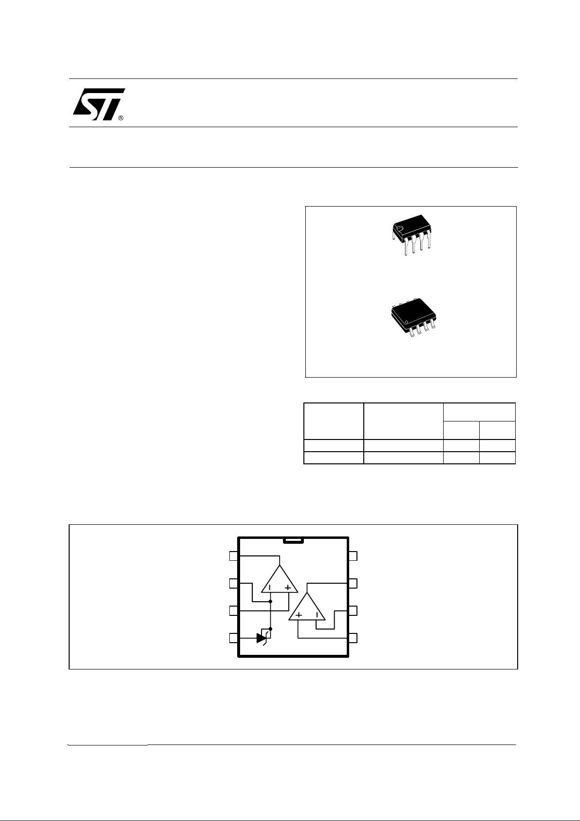
DESCRIPTION
The TSM109 is a monolithic IC that includes two
comparators and a shunt voltage refe rence. This
device offers space and cost savings in many
applications including power supply management
or data acquisition systems.
Package Reference
N
DIP-8
D
SO-8
ORDER CODE
Part
Number
TSM109 -40°C, +105°C ••
TSM109A -40°C, +105°C ••
Note: N = Dual in Line Package (DI P)
D = Smal l Ou tlin e Pa ckag e (S O) - a lso avai la ble in T ape &
Reel (DT)
Temperature
Range
Package
ND
PIN C ONNECTIONS (top view)
February 2004
Out
1
Vref
2
Ve+
3
Gnd
4
Vcc
Out
Ve-
Ve+
8
7
6
5
1/7
TSM109/A Absolute Maximum Ratings
1 ABSOLUTE MAXIMUM RATINGS
Symbol Parameter Value
VCC Supply voltage 36 V
Input Voltage -0.3 to V
Vin
Ik Continuous Cathode current range -100 to 150 mA
Maximum Junction Temperature
T
j
R
ESD Electrostatic Discharge Protection 1.5 kV
OPERATING CONDITIONS
Thermal Resistance Junction to Ambient (SO package)
thja
+0.3
cc
150 °C
175 °C/W
Symbol Parameter Value Unit
Vcc DC Supply Conditions 2 to 36 V
Toper Operational temp eratur e -40 to105 °C
ELECTRICAL CHARACTERISTICS
+
V
= 5V, V
CC
Symbol Parameter Min Typ Max
Total Supply Current, excluding current in the Voltage
I
CC
Reference
V
V
-
= 0V, T
CC
= +5V, no load
CC
= +30V, no load
CC
= 25°C (unless otherwise specified)
amb
0.4
1
1
2.5
Unit
V
Unit
mA
2/7
Electrical Characteristics TSM109/A
2 ELECTRICAL CHARACTERISTICS
COMPARATOR (independent comparator)
+
= +5V, V
V
CC
Symbo
l
Input Offset Voltage - note 1
V
T
io
amb
T
min
Input Offset Current
T
I
I
A
V
V
V
I
OH
I
sink
t
t
1) At output switch point, Vo ≈ 1.4V, Rs = 0 with V
2) The direct ion of the inp ut cur re nt is out of the IC due to th e PNP inpu t stage . This curre nt is esse ntial ly cons tan t, in depen dent of t he
3) The input common-mode voltage of either input signal voltage should not be allowed to go negative by more than 0.3V. The upper end
4) Positive v oltage e xcursi ons of one inp ut may e xceed t he power supply level. A s long as the other inp ut vol tage rema ins wit hin the
5) The response time specified is for a 100mV input step with 5mV overdrive. For larger overdrive signals, 300ns can be obtained
amb
io
T
min
Input Bias Current (I+ or I-) - note
T
ib
amb
T
min
Large Signal Voltage Gain
vd
V
CC
Input Common Mode Voltage Range - note
V
CC
icm
T
amb
T
min
Differential Input Voltage -note
id
Low Level Output Voltage
V
id
OL
T
amb
T
min
High Level Output Current (Vid = 1V)
V
CC
T
amb
T
min
Output Sink Currrent
V
id
Response Time - note 5
re
R
Large Signal Response Time
R
rel
V
state of the output, so no lo ading charge exists on the reference of input lines.
of the comm on-mode voltage range is V
common-mode range, the comparator will provide an a ppropriate output st ate. The low input v oltage state mu st not be less than -0.3V
(or 0.3V below the negative power supply, if used).
-
= GND, T
CC
= +25°C (unless otherwise specified)
amb
= +25°C
≤ T
≤ T
amb
max
= +25°C
≤ T
≤ T
amb
max
= +25°C
≤ T
≤ T
amb
= 15V, RL = 15kΩ, Vo = 1V to 11V
= 30V
max
= +25°C
≤ T
≤ T
amb
= -1V, I
sink
max
= 4mA
= +25°C
≤ T
≤ T
amb
= Vo = 30V
max
= +25°C
≤ T
≤ T
amb
max
= 1V, Vo = 1.5V
= 5.1kΩ connected to V
L
= 5.1kΩ connected to V
L
= +1.4v
(ref)
+
CC
+
, el = TTL,
CC
CC
Parameter
Min. Typ. Max.
2
3
4
+
from 5V to 30V, and over the full common-mode ran ge (0V to V
CC
+
-1.5V.
TSM109
Unit
159mV
325
100
25 250
400
50 200 V/mV
+
0
0
V
CC
V
CC
V
CC
250 400
700
30 150
1
10 20 mA
1.3 µs
300 ns
+
CC
-1.5
+
-2
+
-1.5V).
nA
nA
V
mV
nA
µA
3/7
 Loading...