

®
LOW DROP OR-ing POWER SCHOTTKY DIODE
MAIN PRODUCT CHARACTERISTIC S
STPS20L15D/G
I
F(AV)
V
RRM
20 A
15 V
Tj (max) 125° C
(max) 0.33 V
V
F
K
K
FEATURES AND BENEFITS
VERY LOW F O RW ARD VOLTAG E DROP FOR
LESS POWER DISSIPATION AND REDUCED
HEATSINK SIZE
REVERSE VOLTAGE SUITED TO OR-ing OF 3V,
A
K
A
NC
5V and 12V RAILS
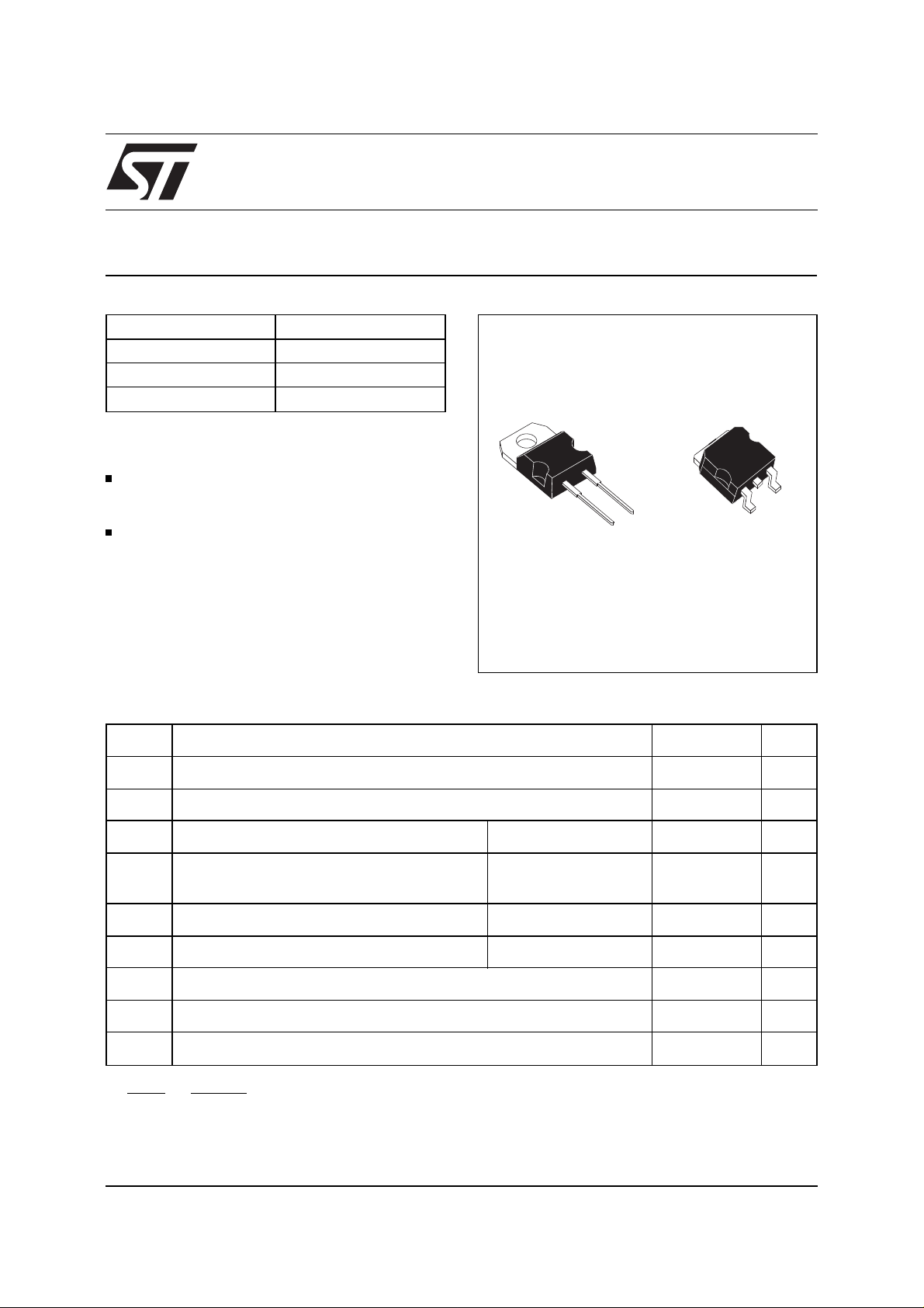
DESCR IPT ION
2
Packaged in TO-220AC or D
PAK, this device is
especially intended for use as an OR-ing diode in
TO-220AC
STPS20L15D
2
PAK
D
STPS20L15G
fault tolerant power supply equipments.
ABSOLUTE RATINGS
(limiting values)
Symbol Parameter Value Unit
V
RRM
Repetitive peak reverse voltage 15 V
I
F(RMS)
I
F(AV)
I
FSM
RMS forward current 30 A
Average forward current Tc = 115°C
Surge non repetitive forward current tp = 10 m s
δ
= 1 20 A
310 A
Sinusoidal
I
RRM
I
RSM
T
stg
Repetitive peak reverse current tp = 2 µs F = 1k Hz 2 A
Non repetitive peak reverse current tp = 100 µs3A
Storage temperature range - 65 to + 150
Tj Maximum operating junction temperature * 125
dV/dt Critical rate of rise of reverse voltage 10000 V /µs
dPtot
* :
July 1999 - Ed: 2B
dTj
<
1
Rth(j−a
thermal runaway condition for a diode on its own heatsink
)
°
C
°
C
1/5
STPS20L15D/G
THERMAL RE SISTA NC ES
Symbol Parameter Value Unit
R
th (j-c)
Junction to case 1.6
°
STATIC ELECTRICAL CHARACTE RISTICS
Symbol Tests Conditions Tests Conditions Min. Typ. Max. Unit
* Reverse leakage
I
R
Tj = 25°CV
= 15V 6 mA
R
current
Tj = 100°CV
* Forward voltage drop Tj = 25°CI
V
F
Tj = 25°CI
Tj = 125°CI
Tj = 125°CI
Pulse test : * tp = 380 µs, δ < 2%
= 15V 200 500
R
= 19 A 0.41 V
F
= 40 A 0.52
F
= 19 A 0.28 0.33
F
= 40 A 0.42 0.50
F
To evaluate the maximum conduction losses use the following equation :
P = 0.18 x I
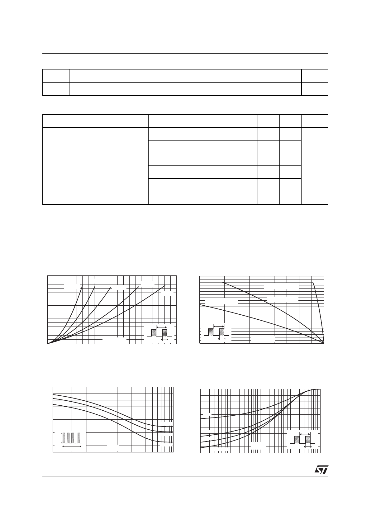
Fig. 1:
Average forward power dissipation versus
average forward current.
PF(av)(W)
8
7
6
5
4
3
2
1
0
0 2 4 6 8 10121416182022
δ = 0.05
+ 8.10-3 x I
F(AV)
δ = 0.1
F2(RMS )
δ = 0.2
IF(av) (A)
δ = 0.5
δ
=tp/T
T
δ = 1
Fig. 2:
Average forward current versus ambient
temperature ( δ = 1).
IF(av)(A)
22
20
18
16
14
Rth(j-a)=35°C/W
12
10
8
6
T
4
2
=tp/T
tp
δ
0
0 25 50 75 100 125
tp
Rth(j-a)=Rth(j-c)
Rth(j-a)=15°C/W
Tamb(°C)
C/W
Fig. 3:
Non repetitive surge peak forward current
versus overload duration (maximum values).
IM(A)
250
200
150
100
I
M
50
0
1E-3 1E-2 1E-1 1E+0
t
δ
=0.5
t(s)
2/5
Tc=50°C
Tc=75°C
Tc=110°C
Fig. 4:
Relative variation of thermal impedance
junction to case versus pulse duration.
Zth(j-c)/Rth(j-c)
1.0
0.8
δ = 0.5
0.6
0.4
δ = 0.2
δ = 0.1
0.2
0.0
1.0E-4 1.0E-3 1.0E-2 1.0E-1 1.0E+0
Single pulse
tp (s)
δ
=tp/T
T
tp

STPS20L15D/G
Fig. 5:
Reverse leakage current versus reverse
voltage applied (typical values).
IR(mA)
5E+2
1E+2
Tj=100°C
1E+1
1E+0
1E-1
0246810121416
Fig. 7:
Forward voltage drop versus forward
Tj=25°C
VR(V)
current (typical values).
IFM(A)
200.0
100.0
Tj=125°C
10.0
1.0
Tj=75°C
Tj=25°C
Fig. 6:
Junction capacitance versus reverse
voltage applied (typical values).
C(nF)
5.0
1.0
VR(V)
0.1
12 51020
Fig. 8:
Forward voltage drop versus forward
F=1MHz
Tj=25°C
current (maximum values).
IFM(A)
200
Tj=100°C
100
10
0.1
0 0.2 0.4 0.6 0.8 1 1.2 1.4 1.6
Fig. 9:
Thermal resistance junction to ambient
VFM(V)
versus copper surface under tab (Epoxy printed
circuit board FR4, copper thickness : 35 µm).
(STPS20L15G only)
Rth(j-a) (°C/W)
80
70
60
50
40
30
20
10
0
0 4 8 1216202428323640
S(Cu) (cm²)
1
0 0.2 0.4 0.6 0.8 1 1.2 1.4 1.6 1.8
VFM(V)
3/5

STPS20L15D/G
PACKAGE MECHANICAL DAT A
2
D
PAK
E
L2
L
L3
B2
B
G
* FLAT ZONE NO LESS THAN 2mm
C2
A1
DIMENSIONS
REF.
Millimeters Inches
Min. Max. Min. Max.
A
A 4.40 4.60 0.173 0.181
A1 2.49 2.69 0.098 0.106
A2 0.03 0.23 0.001 0.009
B 0.70 0.93 0.027 0.037
D
B2 1.14 1.70 0.045 0.067
C 0.45 0.60 0.017 0.024
C2 1.23 1.36 0.048 0.054
D 8.95 9.35 0.352 0.368
C
R
E 10.00 10.40 0.393 0.409
G 4.88 5.28 0.192 0.208
L 15.00 15.85 0.590 0.624
A2
L2 1.27 1.40 0.050 0.055
L3 1.40 1.75 0.055 0.069
M 2.40 3.20 0.094 0.126
M
*
V2
R 0.40 typ. 0.016 typ.
V2 0° 8° 0° 8°
FOOT PRINT DIMENSIONS
16.90
10.30
8.90
(in millimeters)
5.08
1.30
3.70
4/5

PACKAGE MECHANICAL DAT A
TO-220AC
H2
L5
Ø I
L6
L2
L9
F1
L4
F
G
STPS20L15D/G
DIMENSIONS
REF.
A
C
A 4.40 4.60 0.173 0.181
C 1.23 1.32 0.048 0.051
L7
D 2.40 2.72 0.094 0.107
E 0.49 0.70 0.019 0.027
F 0.61 0.88 0.024 0.034
F1 1.14 1.70 0.044 0.066
G 4.95 5.15 0.194 0.202
D
H2 10.00 10.40 0.393 0.409
L2 16.40 typ. 0.645 typ.
L4 13.00 14.00 0.511 0.551
M
E
L5 2.65 2.95 0.104 0.116
L6 15.25 15.75 0.600 0.620
L7 6.20 6.60 0.244 0.259
L9 3.50 3.93 0.137 0.154
M 2.6 typ. 0.102 typ.
Diam. I 3.75 3.85 0.147 0.151
Millimeters Inches
Min. Max. Min. Max.
Ordering type Markin g Package Weight Base qty Delivery mode
STPS20L15D STPS20L15D TO-220AC 1.86 g. 50 Tube
STPS20L15G STPS20L15G D
STPS20L15G-TR STPS20L15G D
2
PAK 1.48g. 50 Tube
2
PAK 1.48 g. 1000 Tape and reel
Cooling method: by conduction (C)
Recommended torque value: 0.55 m.N
Maximum torque value: 0.7 m.N
Epoxy meets UL94,V0
Information furnished is believed to be accurate and reliable. However, STMicroelectronics assumes no responsibility for the co nseq ue nce s of
use of such information nor for any infringement of patents or other rights of third parties which may result from its use. No license is granted by
implication or otherwi se un der any pat ent or patent r ights of STM icroele ctronics. Specifica tions m entioned i n this pub lication are subj ect to
change without notice. This publication supersedes and replaces all information previously supplied.
STMicroelectronics products are not authorized for use as critical components in life support devices or sy st em s without express written approval of STMicroelectronics.
The ST logo is a registered trademark o f STMicroelectron ics
© 1999 STMicroelectronics - Printed in Italy - All rights reserved.
STMicroelectronics GROUP OF COMPANIES
Australia - Brazil - China - Finland - France - Germany - Hong Kong - India - Italy - Japan - Malaysia
Malta - Morocco - Singapore - Spain - Sweden - Switzerland - United Kingdom - U.S.A.
http://www.st.com
5/5
 Loading...