

Page 1
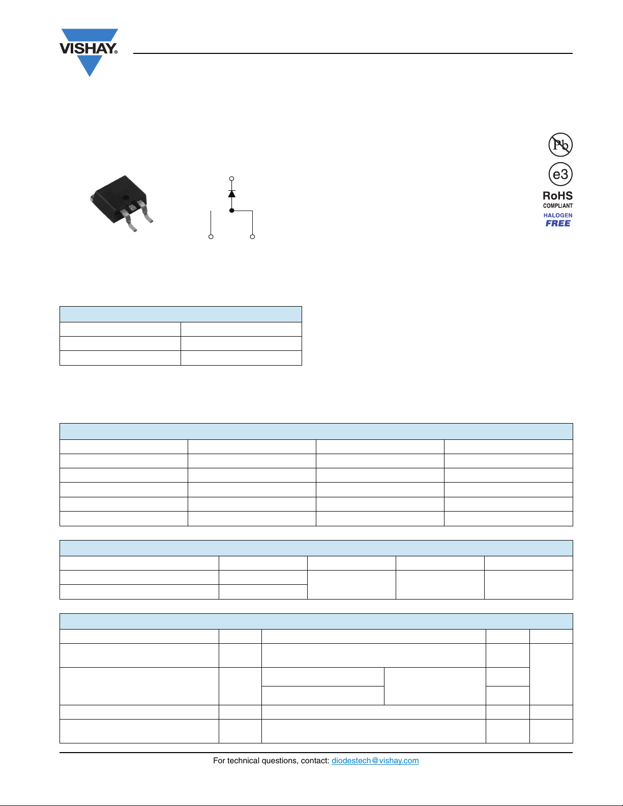
D2PAK
PRODUCT SUMMARY
I
F(AV)
V
R
I
RM
Schottky Rectifier, 20 A
FEATURES
• 125 °C TJ operation (VR < 5 V)
Base
cathode
2
1
N/C
20 A
15 V
600 mA at 100 °C
3
Anode
• Center tap module
• Optimized for OR-ing applications
• Ultralow forward voltage drop
• High frequency operation
• Guard ring for enhanced ruggedness and long
term reliability
• High purity, high temperature epoxy
encapsulation for enhanced mechanical strength and
moisture resistance
• Meets MSL level 1, per J-STD-020, LF maximum peak of
260 °C
• Halogen-free according to IEC 61249-2-21 definition
• Compliant to RoHS directive 2002/95/EC
• AEC-Q101 qualified
DESCRIPTION
The Schottky rectifier module has been optimized for
ultralow forward voltage drop specifically for the OR-ing
of parallel power supplies. The proprietary barrier
technology allows for reliable operation up to 125 °C
junction temperature. Typical applications are in parallel
switching power supplies, converters, reverse battery
protection, and redundant power subsystems.
VS-STPS20L15GPbF
Vishay High Power Products
MAJOR RATINGS AND CHARACTERISTICS
SYMBOL CHARACTERISTICS VALUES UNITS
I
F(AV)
V
I
FSM
V
T
RRM
F
J
Rectangular waveform 20 A
15 V
tp = 5 μs sine 700 A
19 Apk, TJ = 125 °C (typical) 0.25 V
Range - 55 to 125 °C
VOLTAGE RATINGS
PARAMETER SYMBOL TEST CONDITIONS VS-STPS20L15GPbF UNITS
Maximum DC reverse voltage V
Maximum working peak reverse voltage V
R
RWM
TJ = 100 °C 15 V
ABSOLUTE MAXIMUM RATINGS
PARAMETER SYMBOL TEST CONDITIONS VALUES UNITS
Maximum average forward current
See fig. 5
Maximum peak one cycle
non-repetitive surge current
See fig. 7
Non-repetitive avalanche energy E
Repetitive avalanche current I
Document Number: 94326 For technical questions, contact: diodestech@vishay.com
Revision: 16-Mar-10 1
I
F(AV)
I
FSM
50 % duty cycle at TC = 85 °C, rectangular waveform 20
5 μs sine or 3 μs rect. pulse
10 ms sine or 6 ms rect. pulse 330
TJ = 25 °C, IAS = 2 A, L = 6 mH 10 mJ
AS
AR
Current decaying linearly to zero in 1 μs
Frequency limited by T
maximum VA = 1.5 x VR typical
J
Following any rated load
condition and with rated
V
applied
RRM
700
2A
www.vishay.com
A
Page 2
VS-STPS20L15GPbF
Vishay High Power Products
Schottky Rectifier, 20 A
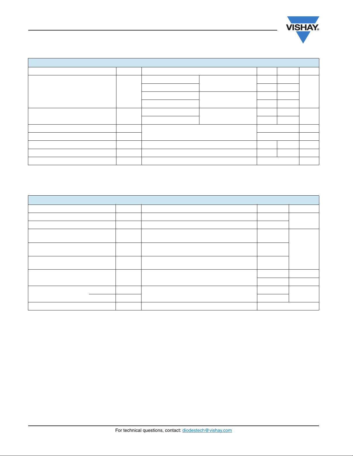
ELECTRICAL SPECIFICATIONS
PARAMETER SYMBOL TEST CONDITIONS TYP. MAX. UNITS
19 A
Forward voltage drop
See fig. 1
V
FM
40 A - 0.52
(1)
19 A
40 A 0.37 0.50
Reverse leakage current
See fig. 2
I
RM
Threshold voltage V
Forward slope resistance r
Maximum junction capacitance C
Typical series inductance L
F (TO)
TJ = 25 °C
(1)
T
= 100 °C - 600
J
TJ = TJ maximum
t
VR = 5 VDC (test signal range 100 kHz to 1 MHz), 25 °C - 2000 pF
T
Measured lead to lead 5 mm from package body 8 - nH
S
Maximum voltage rate of change dV/dt Rated V
T
= 25 °C
J
= 125 °C
T
J
V
= Rated V
R
R
R
-0.41
0.25 0.33
-10
0.182 V
7.6 mΩ
10 000 V/μs
Note
(1)
Pulse width < 300 μs, duty cycle < 2 %
THERMAL - MECHANICAL SPECIFICATIONS
PARAMETER SYMBOL TEST CONDITIONS VALUES UNITS
Maximum junction temperature range T
Maximum storage temperature range T
Maximum thermal resistance,
junction to case
Typical thermal resistance,
case to heatsink
Maximum thermal resistance,
junction to ambient
J
Stg
DC operation
R
thJC
R
thCS
R
thJA
See fig. 4
Mounting surface, smooth and greased (for TO-220) 0.50
DC operation (for D2PAK) 40
Approximate weight
Mounting torque
minimum
maximum 12 (10)
Non-lubricated threads
Marking device Case style D
2
PAK STPS20L15G
- 55 to 125
- 55 to 150
°C
1.5
°C/W
2g
0.07 oz.
6 (5)
kgf · cm
(lbf · in)
V
mA
www.vishay.com For technical questions, contact: diodestech@vishay.com
Document Number: 94326
2 Revision: 16-Mar-10
Page 3
VS-STPS20L15GPbF
Schottky Rectifier, 20 A
1000
100
10
- Instantaneous
F
I
Forward Current (A)
1
0.2 0.4 0.6 0.8 1.2
0
V
- Forward Voltage Drop (V)
FM
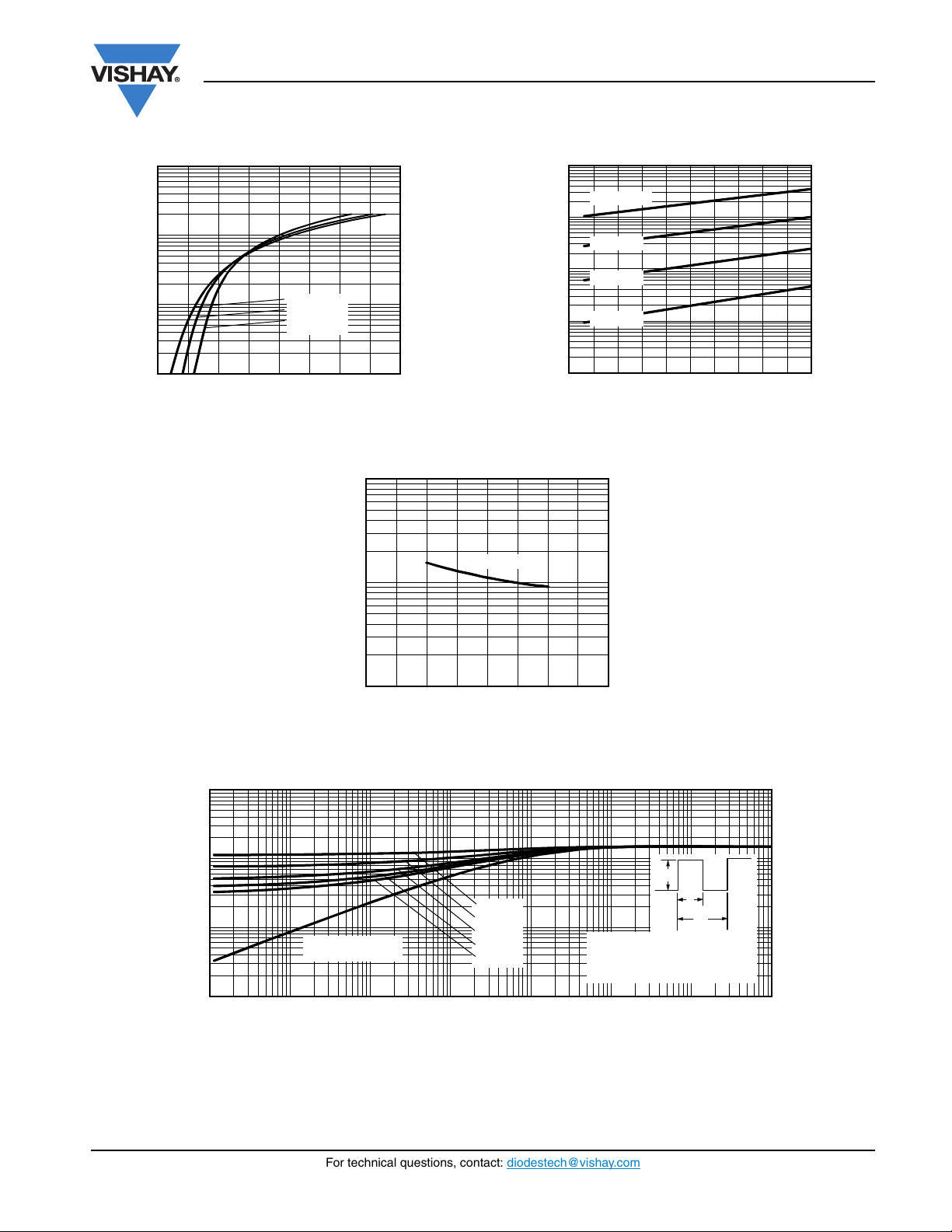
Fig. 1 - Maximum Forward Voltage Drop Characteristics
TJ = 125 °C
T
= 75 °C
J
= 25 °C
T
J
1.0
10 000
1.4
1.6
Vishay High Power Products
1000
TJ = 100 °C
100
TJ = 75 °C
10
TJ = 50 °C
TJ = 25 °C
1
- Reverse Current (mA)
R
I
0.1
0
V
- Reverse Voltage (V)
R
Fig. 2 - Typical Values of Reverse Current vs.
63912
15
Reverse Voltage
TJ = 25 °C
1000
- Junction Capacitance (pF)
T
C
100
0
V
R
10515
- Reverse Voltage (V)
Fig. 3 - Typical Junction Capacitance vs. Reverse Voltage
10
1
D = 0.75
0.1
- Thermal Impedance (°C/W)
thJC
Z
0.01
0.00001 0.0001 0.001 0.01 0.1 1
Single pulse
(thermal resistance)
D = 0.50
D = 0.33
D = 0.25
D = 0.20
t1 - Rectangular Pulse Duration (s)
20
P
DM
Notes:
1. Duty factor D = t
2. Peak TJ = PDM x Z
1/t2
t
1
thJC
t
2
+ T
C
100 10
Fig. 4 - Maximum Thermal Impedance Z
Characteristics
thJC
Document Number: 94326 For technical questions, contact: diodestech@vishay.com
www.vishay.com
Revision: 16-Mar-10 3
Page 4
VS-STPS20L15GPbF
Vishay High Power Products
100
95
90
85
Square wave (D = 0.50)
80
75
Allowable Case Temperature (°C)
See note (1)
70
0
I
F(AV)
84 121620
- Average Forward Current (A)
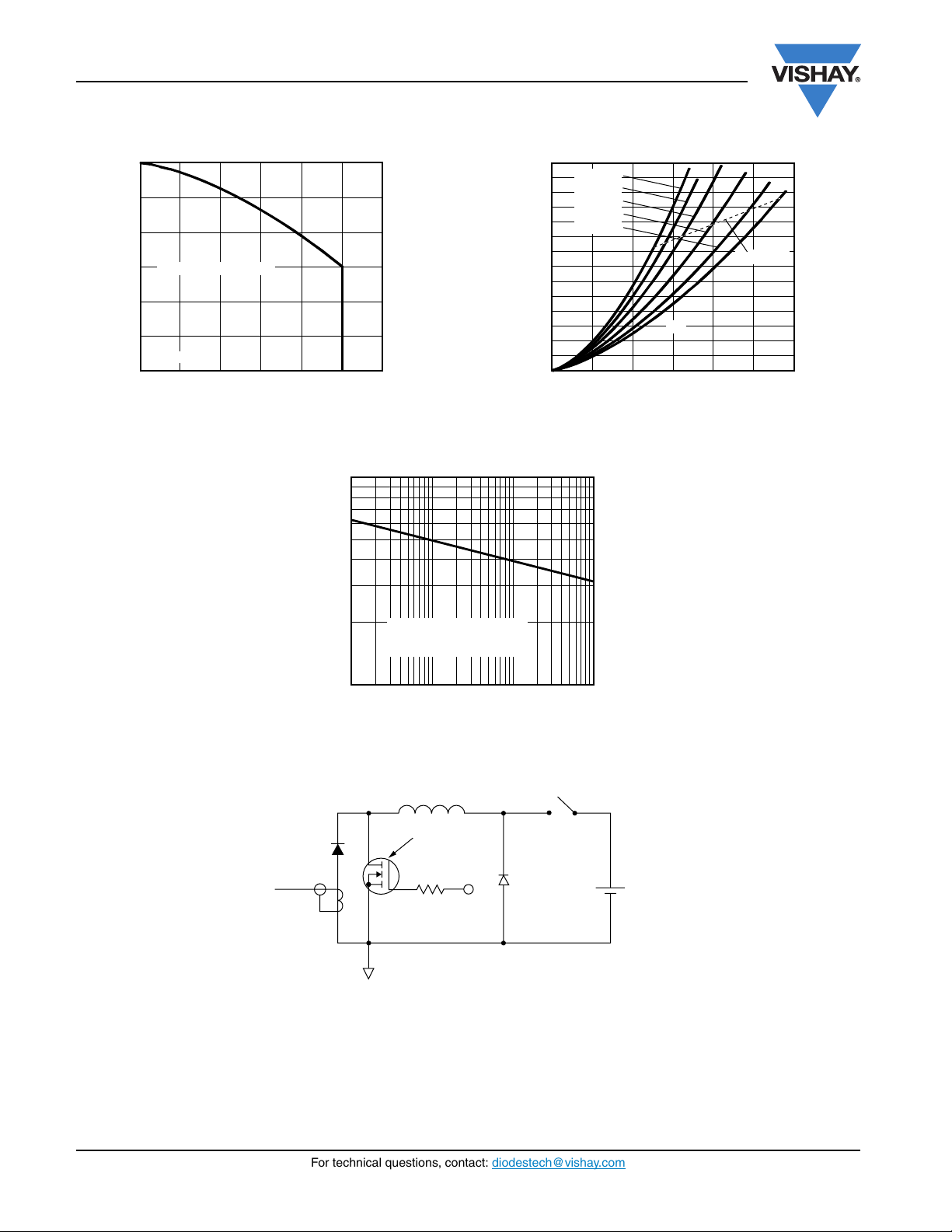
Fig. 5 - Maximum Allowable Case Temperature vs.
Average Forward Current
1000
Schottky Rectifier, 20 A
14
12
10
8
6
4
Average Power Loss (W)
2
0
24
0
Fig. 6 - Forward Power Loss Characteristics
D = 0.20
D = 0.25
D = 0.33
D = 0.50
D = 0.75
DC
1051520
I
- Average Forward Current (A)
F(AV)
RMS limit
3025
Note
(1)
Formula used: TC = TJ - (Pd + Pd
Pd = Forward power loss = I
Pd
= Inverse power loss = VR1 x IR (1 - D); IR at VR1 = 80 % rated V
REV
Current
monitor
x VFM at (I
F(AV)
At any rated load condition
and with rated V
following surge
- Non-Repetitive Surge Current (A)
100
FSM
I
10
100 1000
tp - Square Wave Pulse Duration (µs)
Fig. 7 - Maximum Non-Repetitive Surge Current
L
D.U.T.
IRFP460
= 25 Ω
R
g
Fig. 8 - Unclamped Inductive Test Circuit
) x R
REV
;
thJC
/D) (see fig. 6);
F(AV)
RRM
applied
R
High-speed
switch
Freewheel
diode
40HFL40S02
10 000
V
= 25 V
d
+
www.vishay.com For technical questions, contact: diodestech@vishay.com
Document Number: 94326
4 Revision: 16-Mar-10
Page 5
Document Number: 94326 For technical questions, contact: diodestech@vishay.com
www.vishay.com
Revision: 16-Mar-10 5
VS-STPS20L15GPbF
Schottky Rectifier, 20 A
Vishay High Power Products
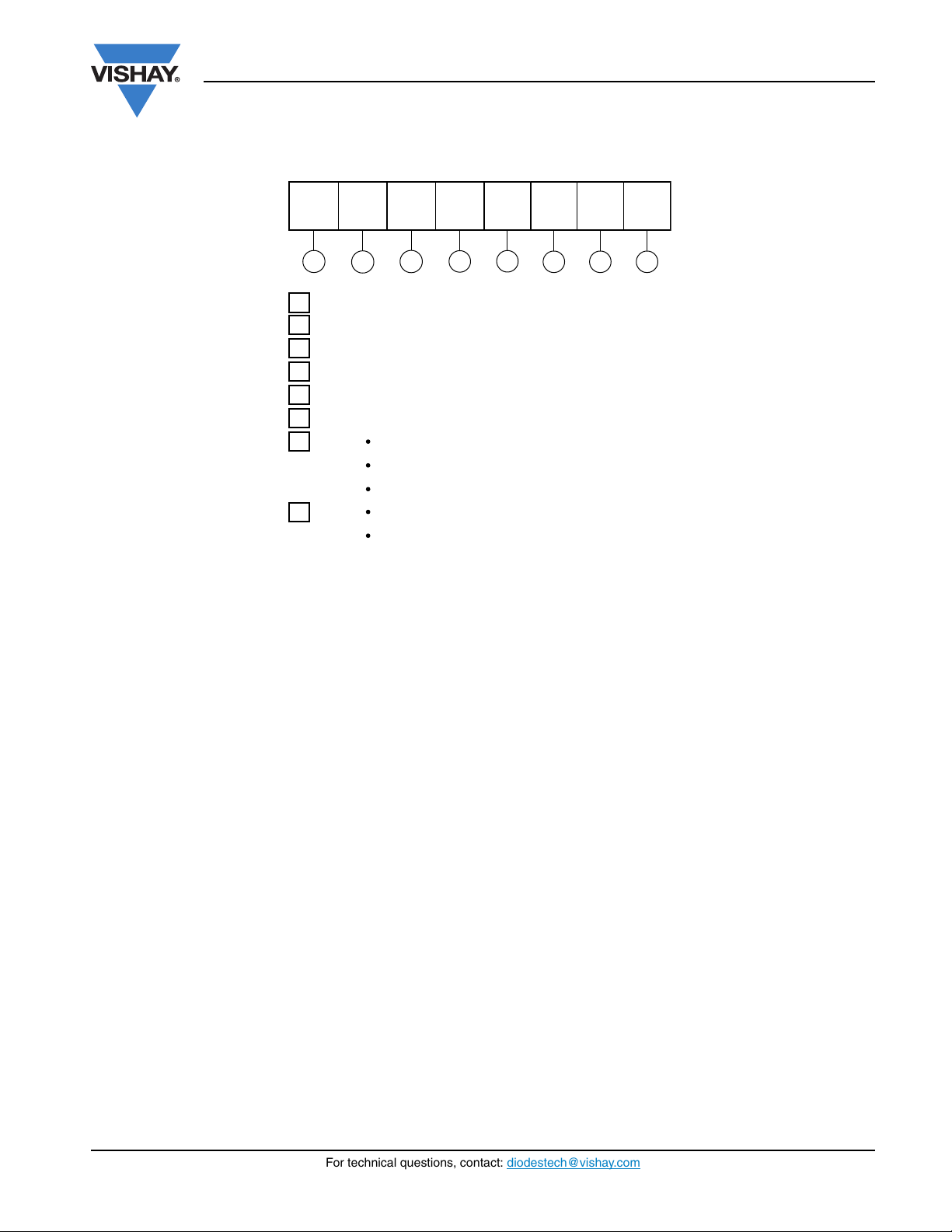
ORDERING INFORMATION TABLE
2 - Essential part number
3
- Current rating (20 = 20 A)
4
- Low voltage
5 - Voltage rating (15 = 15 V)
- G = D
2
PAK package
6
7
-
None = Tube (50 pieces)
TRL = Tape and reel (left oriented)
-
PbF = Lead (Pb)-free (for D2PAK tube)
P = Lead (Pb)-free (for D2PAK TRR and TRL)
TRR = Tape and reel (right oriented)
8
1 - HPP product suffix
Device code
51 324678
VS- STPS 20 L 15 G TRL PbF
Page 6
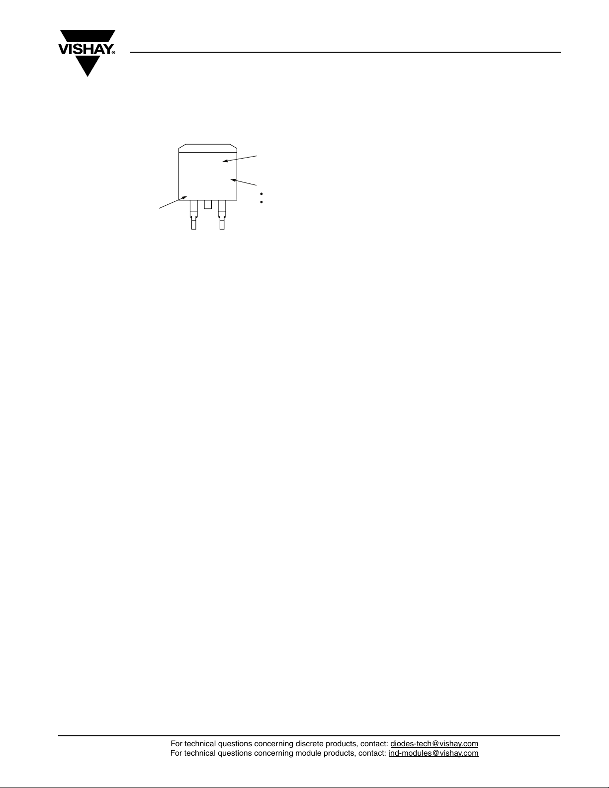
D2PAK
Part Marking Information
Vishay High Power Products
Assembly
lot code
xxxxxxS
V PYWWXA
8024
Part number
Product version (optional):
P = Lead (Pb)-free
None = Standard
Date code:
Year 0 = 2000
Week 02
Line X
Child lot A
Example: This is a xxxxxxS with
assembly lot code 8024,
assembled on WW 02, 2000
Document Number: 95054 For technical questions concerning discrete products, contact: diodes-tech@vishay.com
Revision: 17-Oct-08 For technical questions concerning module products, contact: ind-modules@vishay.com
www.vishay.com
1
Page 7
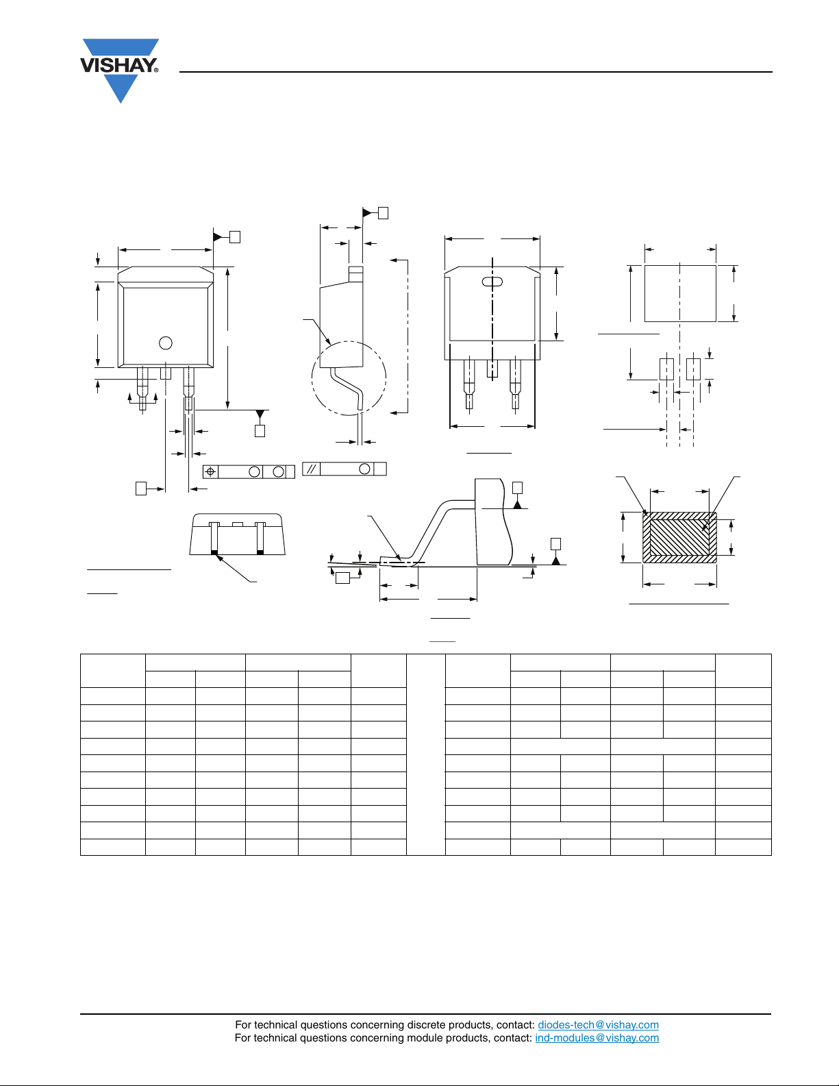
DIMENSIONS in millimeters and inches
Outline Dimensions
Vishay High Power Products
D2PAK
Conforms to JEDEC outline D
(2)(3)
E
(3)
L1
D
L2
2 x
Lead assignments
Diodes
1. - Anode (two die)/open (one die)
2., 4. - Cathode
3. - Anode
4
132
BB
e
2
H
2 x b2
2 x b
0.010
PAK (SMD-220)
A
Detail A
(2)
C
MM
A
Lead tip
B
A
c2
AA
A
c
M
± 0.004
B
Gauge
0° to 8°
plane
L3
B
L
L4
Detail “A”
Rotated 90 °CW
Scale: 8:1
(E)
E1
View A - A
A1
(3)
(D1)
17.90 (0.70)
15.00 (0.625)
2.32
(0.08)
Plating
Seating
plane
2.64 (0.103)
2.41 (0.096)
(3)
H
B
Pad layout
11.00
MIN.
(0.43)
MIN.
(4)
b1, b3
(c)
(b, b2)
Section B - B and C - C
Scale: None
9.65
(0.38)
3.81
(0.15)
c1
MIN.
MIN.
Base
Metal
(4)
SYMBOL
MILLIMETERS INCHES
MIN. MAX. MIN. MAX. MIN. MAX. MIN. MAX.
NOTES SYMBOL
MILLIMETERS INCHES
NOTES
A 4.06 4.83 0.160 0.190 D1 6.86 8.00 0.270 0.315 3
A1 0.00 0.254 0.000 0.010 E 9.65 10.67 0.380 0.420 2, 3
b 0.51 0.99 0.020 0.039 E1 7.90 8.80 0.311 0.346 3
b1 0.51 0.89 0.020 0.035 4 e 2.54 BSC 0.100 BSC
b2 1.14 1.78 0.045 0.070 H 14.61 15.88 0.575 0.625
b3 1.14 1.73 0.045 0.068 4 L 1.78 2.79 0.070 0.110
c 0.38 0.74 0.015 0.029 L1 - 1.65 - 0.066 3
c1 0.38 0.58 0.015 0.023 4 L2 1.27 1.78 0.050 0.070
c2 1.14 1.65 0.045 0.065 L3 0.25 BSC 0.010 BSC
D 8.51 9.65 0.335 0.380 2 L4 4.78 5.28 0.188 0.208
Notes
(1)
Dimensioning and tolerancing per ASME Y14.5 M-1994
(2)
Dimension D and E do not include mold flash. Mold flash shall not exceed 0.127 mm (0.005") per side. These dimensions are measured at
the outmost extremes of the plastic body
(3)
Thermal pad contour optional within dimension E, L1, D1 and E1
(4)
Dimension b1 and c1 apply to base metal only
(5)
Datum A and B to be determined at datum plane H
(6)
Controlling dimension: inch
(7)
Outline conforms to JEDEC outline TO-263AB
Document Number: 95046 For technical questions concerning discrete products, contact: diodes-tech@vishay.com
www.vishay.com
Revision: 31-Mar-09 For technical questions concerning module products, contact: ind-modules@vishay.com
1
Page 8
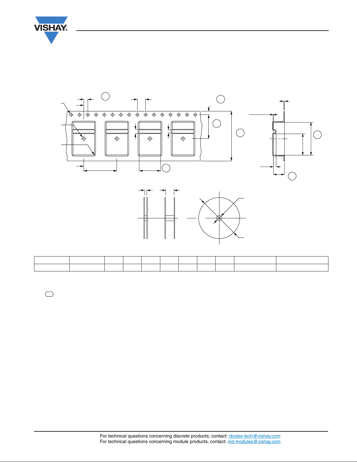
D2PAK
CARRIER TAPE FOR TAPE AND REEL LEFT in millimeters
Carrier tape (130 meter long per reel)
C
7
Ø 1.55 ± 0.05
Ø 1.6 ± 0.1
R 0.3
typical
P
2
Y
2.0 ± 0.1
2.17 ± 0.1
P
0
4.0 ± 0.1
1.57 ± 0.1
Packaging Information
Vishay High Power Products
C
L
0.40 ± 0.05
B
2
± 0.1
C
6
1.75 ± 0.1
C
4
F ± 0.1
C
5
W ± 0.3
0.12 MAX.
C
B
2
± 0.1
0
Ø 72
Ø 560
1.20
Section Y - Y
K
0
Y
P1 ± 0.1 A0 ± 0.1
NUMBER PACKAGE A
93-0194-01 D
2
PAK 10.80 16.00 10.35 4.90 11.50 16.00 24.00 330 800
C
1
Reel
30
Single
winded
B
0
0
winded
B
2
Level
K
114
FP1W REEL DIAMETER QUANTITY PER REEL
0
Notes
MATERIAL
1. General
• : Statistical, C
ST
≥ 1.33
pk
• 10 sprocket hole pitch cumulative tolerance ± 0.02 mm
• Camber not to exceed 1 mm in 250 mm
• A
and B0 measured on a plane 0.3 mm above the bottom of
0
the pocket
• K
measured from a plane on the inside bottom of the pocket to
0
the top surface of the carrier
• Pocket position relative to sprocket hole measured as true
PACKAGING
1. General
• Each box must be identified with Vishay part number 93-0194-x
• Box should be free of foreign particles
• Product must be stored at room temperature and clean
environment
• Certificate of analysis is required per every lot number
2. Material
• Conductive black styrenic alloy
position of pocket, not pocket hole
• Measured from centerline of sprocket hole to centerline of
pocket
• Must also meet requirements of EIA standard #EIA-481A
taping of surface mount components for automatic placement
2. Specification
• Poliestyrene
• Surface resistivity of molded material must measure
6
≤ 10
Ω/SQ measured in accordance to procedure given in
ASTM D-257 and ASTM D-991
• Free of heat marks
• No sharp edges allowed
• No deformities allowed in wall cavity
• Holes, edges and cavities must be free of burrs ≤ 0.060 mm
(burrs shall not come off the tape)
Document Number: 95032 For technical questions concerning discrete products, contact: diodes-tech@vishay.com
Revision: 18-May-09 For technical questions concerning module products, contact: ind-modules@vishay.com
± 0.1
C
3
www.vishay.com
1
Page 9
Packaging Information
Vishay High Power Products
D2PA K
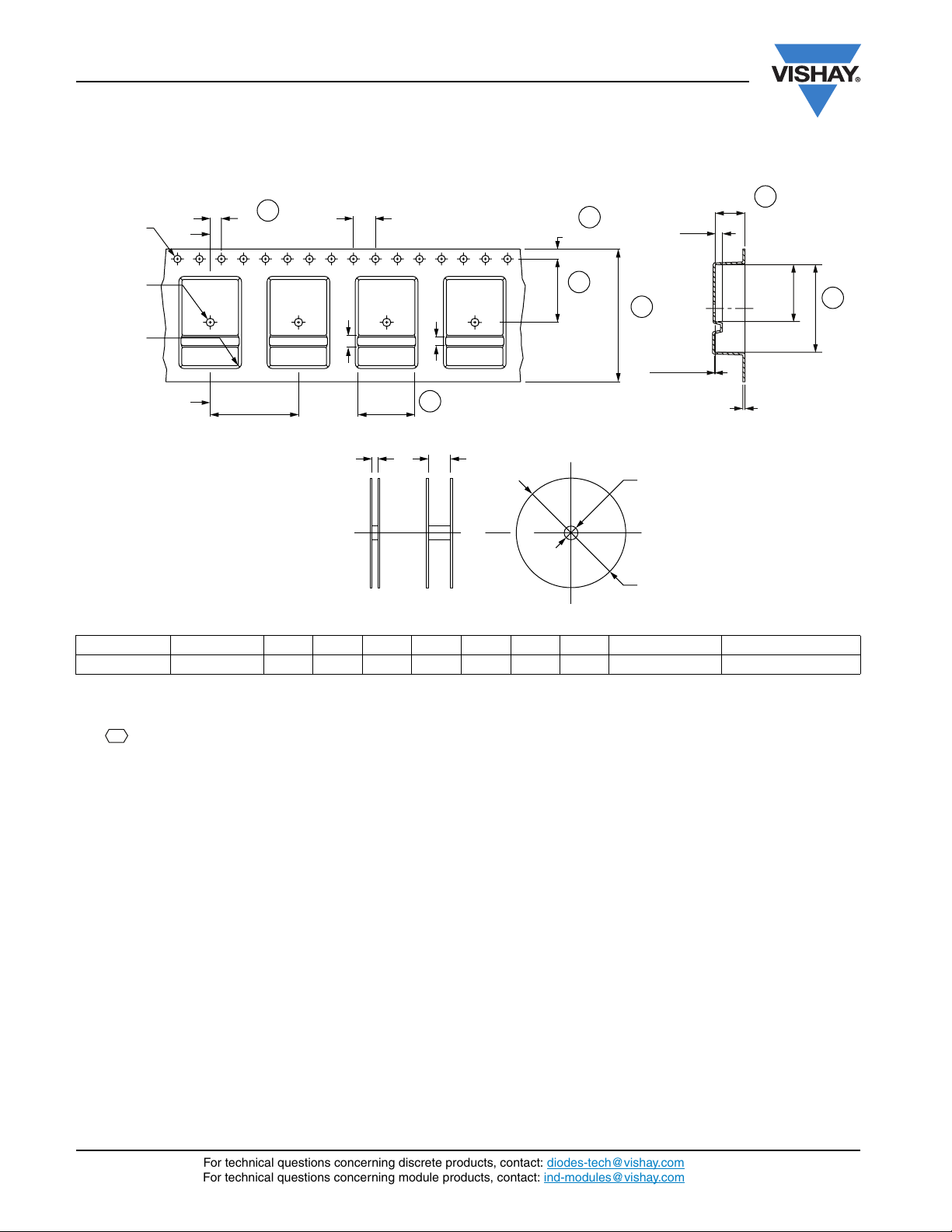
CARRIER TAPE FOR TAPE AND REEL RIGHT in millimeters
Carrier tape (130 meter long per reel)
C
Ø 1.55 ± 0.05
Ø 1.6 ± 0.1
R 0.3
typical
6
P
2
Y
Y
2.0 ± 0.1
2.17 ± 0.1
P1 ± 0.1
30
A0 ± 0.1
P
0
4.0 ± 0.1
C
1.57 ± 0.1
1
Reel
114
C
7
1.75 ± 0.1
C
4
F ± 0.1
C
5
W ± 0.3
Ø 72
1.20
0.12 MAX.
K
0
C
L
0.40 ± 0.05
Section Y - Y
± 0.1
B
C
3
± 0.1
2
C
B
2
± 0.1
0
Single
winded
NUMBER PACKAGE A
93-0195-01 D
2
PAK 10.80 16.00 10.35 4.90 11.50 16.00 24.00 330 800
B
0
B
0
2
Notes
MATERIAL
1. General
• : Statistical, C
ST
≥ 1.33
pk
• 10 sprocket hole pitch cumulative tolerance ± 0.02 mm
• Camber not to exceed 1 mm in 250 mm
• A
and B0 measured on a plane 0.3 mm above the bottom of
0
the pocket
• K
measured from a plane on the inside bottom of the pocket to
0
the top surface of the carrier
• Pocket position relative to sprocket hole measured as true
position of pocket, not pocket hole
• Measured from centerline of sprocket hole to centerline of
pocket
• Must also meet requirements of EIA standard #EIA-481A
taping of surface mount components for automatic placement
2. Specification
• Poliestyrene
• Surface resistivity of molded material must measure
6
≤ 10
Ω/SQ measured in accordance to procedure given in
ASTM D-257 and ASTM D-991
• Free of heat marks
• No sharp edges allowed
• No deformities allowed in wall cavity
• Holes, edges and cavities must be free of burrs ≤ 0.060 mm
(burrs shall not come off the tape)
Level
winded
K
0
Ø 560
FP1W REEL DIAMETER QUANTITY PER REEL
PACKAGING
1. General
• Each box must be identified with Vishay part number 93-0195-x
• Box should be free of foreign particles
• Product must be stored at room temperature and clean
environment
• Certificate of analysis is required per every lot number
2. Material
• Conductive black styrenic alloy
www.vishay.com For technical questions concerning discrete products, contact: diodes-tech@vishay.com
2 For technical questions concerning module products, contact: ind-modules@vishay.com
Document Number: 95032
Revision: 18-May-09
Page 10
Packaging Information
D2PA K
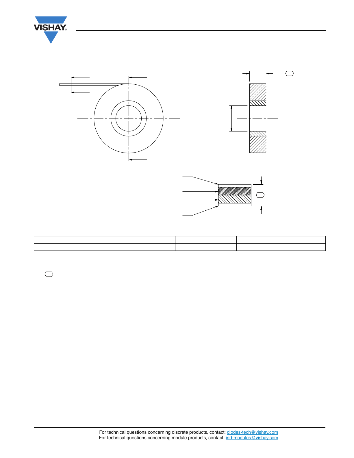
COVER TAPE FOR CARRIER TAPE in millimeters
Y
Y
X
X
Antistatic layer
Pet layer
Olefin layer
Vishay High Power Products
W
ST
Ø 76.5 ± 1.0
Section X - X
0.055 ± 0.005
ST
Sealant layer
Section Y - Y
VERSION NUMBER APPLICATION W CARRIER TAPE WIDTH MATERIAL
01 92-5210-14 D
Notes
MATERIAL
1. General
• : C
2. Specification
ST
≥ 1.33
pk
2
PAK 21.3 ± 0.1 24 Antistatic/treated/transparent/polyester
PACKAGING
1. General
• Each box must be identified with Vishay part number 92-5210-x
• Box should be free of foreign particles
• Thickness: 0.052 ± 0.005
• Length: 500 m
• Tensile strength: 6.00 kg/mm SQ
• Elongation: > 100 %
• Surface resistivity: 10E11 Ω/SQ max. both sides (antistatic)
• Peel strength conforms to IRMX specification P01-0074
• POS test range not to exceed 35 grf.
Data included on C of C of every lot
• Curl 4.5 mm max.
Sample length 200 mm
Frequency 5 times
• Inspection date < one year
• Luminous transmittance: 89.8 %
• Must also meet all requirements of EIA-standard #EIA-481C,
taping of surface mount components for automatic placement
• Free of heat marks
• No sharp edges allowed
• No burrs allowed
Document Number: 95032 For technical questions concerning discrete products, contact: diodes-tech@vishay.com
Revision: 18-May-09 For technical questions concerning module products, contact: ind-modules@vishay.com
www.vishay.com
3
Page 11

Legal Disclaimer Notice
Vishay
Disclaimer
All product specifications and data are subject to change without notice.
Vishay Intertechnology, Inc., its affiliates, agents, and employees, and all persons acting on its or their behalf
(collectively, “Vishay”), disclaim any and all liability for any errors, inaccuracies or incompleteness contained herein
or in any other disclosure relating to any product.
Vishay disclaims any and all liability arising out of the use or application of any product described herein or of any
information provided herein to the maximum extent permitted by law. The product specifications do not expand or
otherwise modify Vishay’s terms and conditions of purchase, including but not limited to the warranty expressed
therein, which apply to these products.
No license, express or implied, by estoppel or otherwise, to any intellectual property rights is granted by this
document or by any conduct of Vishay.
The products shown herein are not designed for use in medical, life-saving, or life-sustaining applications unless
otherwise expressly indicated. Customers using or selling Vishay products not expressly indicated for use in such
applications do so entirely at their own risk and agree to fully indemnify Vishay for any damages arising or resulting
from such use or sale. Please contact authorized Vishay personnel to obtain written terms and conditions regarding
products designed for such applications.
Product names and markings noted herein may be trademarks of their respective owners.
Document Number: 91000 www.vishay.com
Revision: 18-Jul-08 1
 Loading...