

Page 1
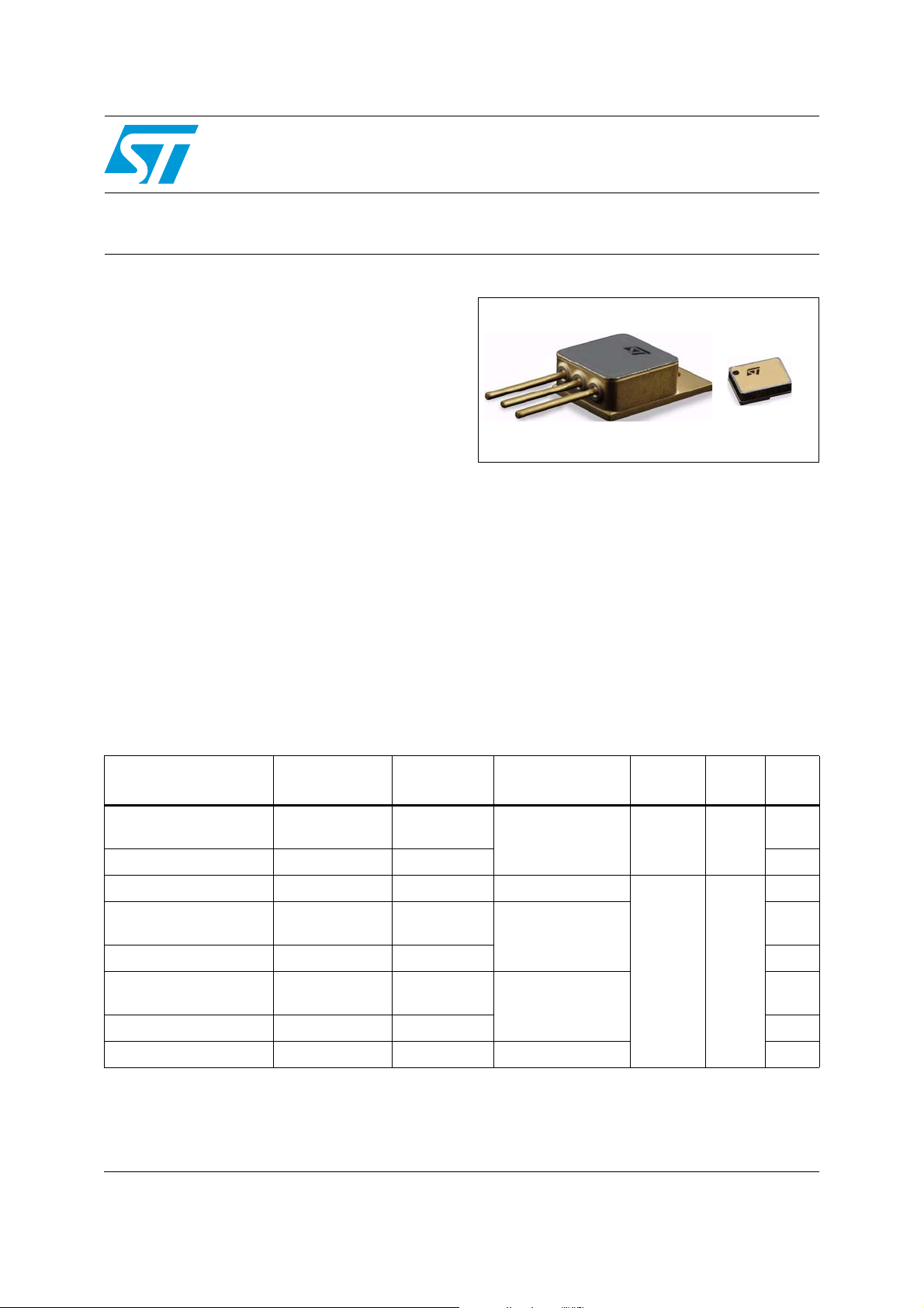
Aerospace 1 x 20 and 2 x 20 A - 100 V Schottky rectifier
Features
■ Forward current: 1 x 20 and 2 x 20 A
■ Repetitive peak voltage: 100 V
■ Low forward voltage drop: 0.8 V
■ Maximum junction temperature: 175 °C
■ Negligible switching losses
■ Low capacitance
■ High reverse avalanche surge capability
■ Hermetic packages
■ Target radiation qualification:
– 150 krad (Si) low dose rate
– 1 Mrad high dose rate
■ ESCC qualified
STPS20100HR
TO-254
Description
This power Schottky rectifier is designed and
packaged to comply with the ESCC5000
specification for aerospace products. Housed in
hermetically sealed packages both surface mount
and through hole, it is ideal for use in applications
for aerospace and other harsh environments.
SMD.5
The STPS20100HR is intended for use in medium
voltage application and particularly, in high
frequency circuits where low switching losses and
low noise are required.
Table 1. Device summary
Order code
STPS20100S1 -
STPS20100SHRB 5106/016/05 ESCC flight -
STPS20100FSYHRB 5106/016/01 ESCC flight Single die
STPS20100AFSY1 -
STPS20100AFSYHRB 5106/016/02 ESCC flight Y
STPS20100CFSY1 -
STPS20100CFSYHRB 5106/016/03 ESCC flight Y
STPS20100SFSYHRB 5106/016/04 ESCC flight Double die, serial Y
ESCC detailed
specification
Quality level Configuration Package Mass EPPL
Engineering
model
Engineering
model
Engineering
model
Single die SMD.5 2.0 g
Double die,
common anode
TO-254 10.0 g
Double die,
common cathode
-
-
-
-
March 2010 Doc ID 16953 Rev 1 1/10
www.st.com
10
Page 2
Characteristics STPS20100HR
1 Characteristics
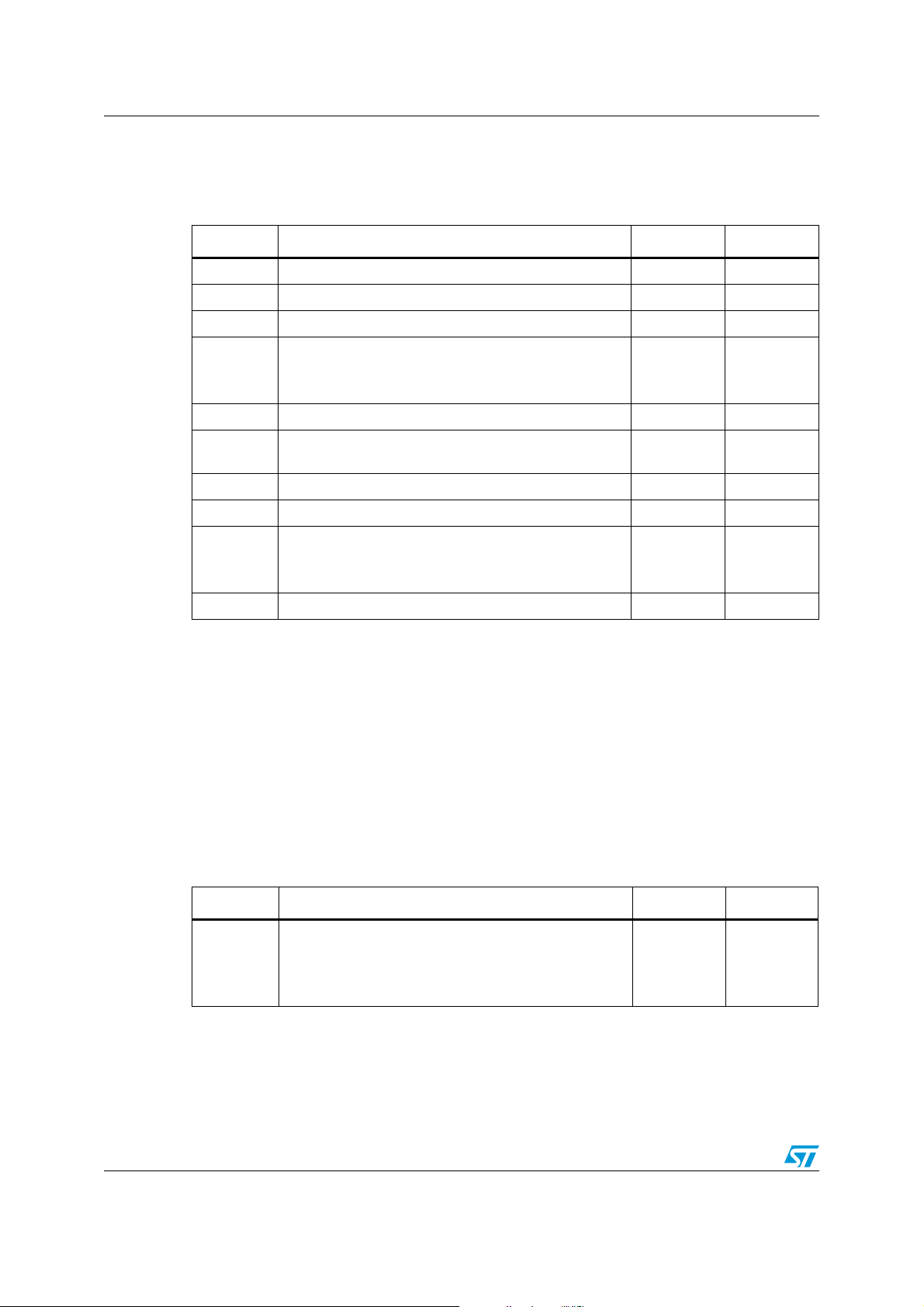
Table 2. Absolute maximum ratings
Symbol Characteristic Value Unit
(6)
(6)
(3)
(2)
(1)
(4), (5)
250 A
100 V
1A
20
A
40
-65 to +175 °C
-65 to +175 °C
+260
oC
+245
I
FSM
V
RRM
I
RRM
I
O
I
F(RMS)
T
OP
T
T
STG
T
SOL
Forward surge current (per diode)
Repetitive peak reverse voltage
Repetitive peak reverse current
Average output rectified current (50% duty cycle):
All variants (per diode)
Variants 02, and 03 (per device)
Forward rms current (per diode) 30 A
Operating temperature range
(case temperature)
Junction temperature +175 °C
J
Storage temperature range
Soldering temperature:
For TO-254
For SMD.5
(7)
(8)
dV/dt Critical rate of rise of reverse voltage 10000 V/µs
1. Sinusoidal pulse of 10 ms duration
2. Pulsed, duration 5 ms, F = 50 Hz
3. Pulsed, duration 2 µs, F = 1 kHz
4. For T
5. The “per Device” ratings apply only as follows:
Variant 02: when both cathode terminals are tied together
Variant 03: when both anode terminals are tied together.
6. For variants with hot solder dip lead finish all testing performed at T
inert atmosphere.
7. Duration 10 seconds maximum at a distance of not less than 1.5 mm from the device body and the same
lead shall not be resoldered until 3 minutes have elapsed.
8. Duration 5 seconds maximum and the same package shall not be resoldered until 3 minutes have elapsed.
Table 3. Thermal resistance
> +140 °C, derate linearly to 0 A at +175 °C.
case
> +125 °C are carried out in a 100%
amb
Symbol Characteristic Value Unit
Thermal resistance, junction to case
th(j-c)
1. Package mounted on infinite heatsink
2. The per device ratings apply for variant 02 when both cathode terminals are tied together and for variant 03
when when both anode terminals are tied togther.
Variants 02, 03 and 04 (per diode)
Variants 02, and 03 (per device)
(2)
Variants 01, and 05
(1)
R
1.65
1.65
0.85
°C/W
2/10 Doc ID 16953 Rev 1
Page 3
STPS20100HR Characteristics
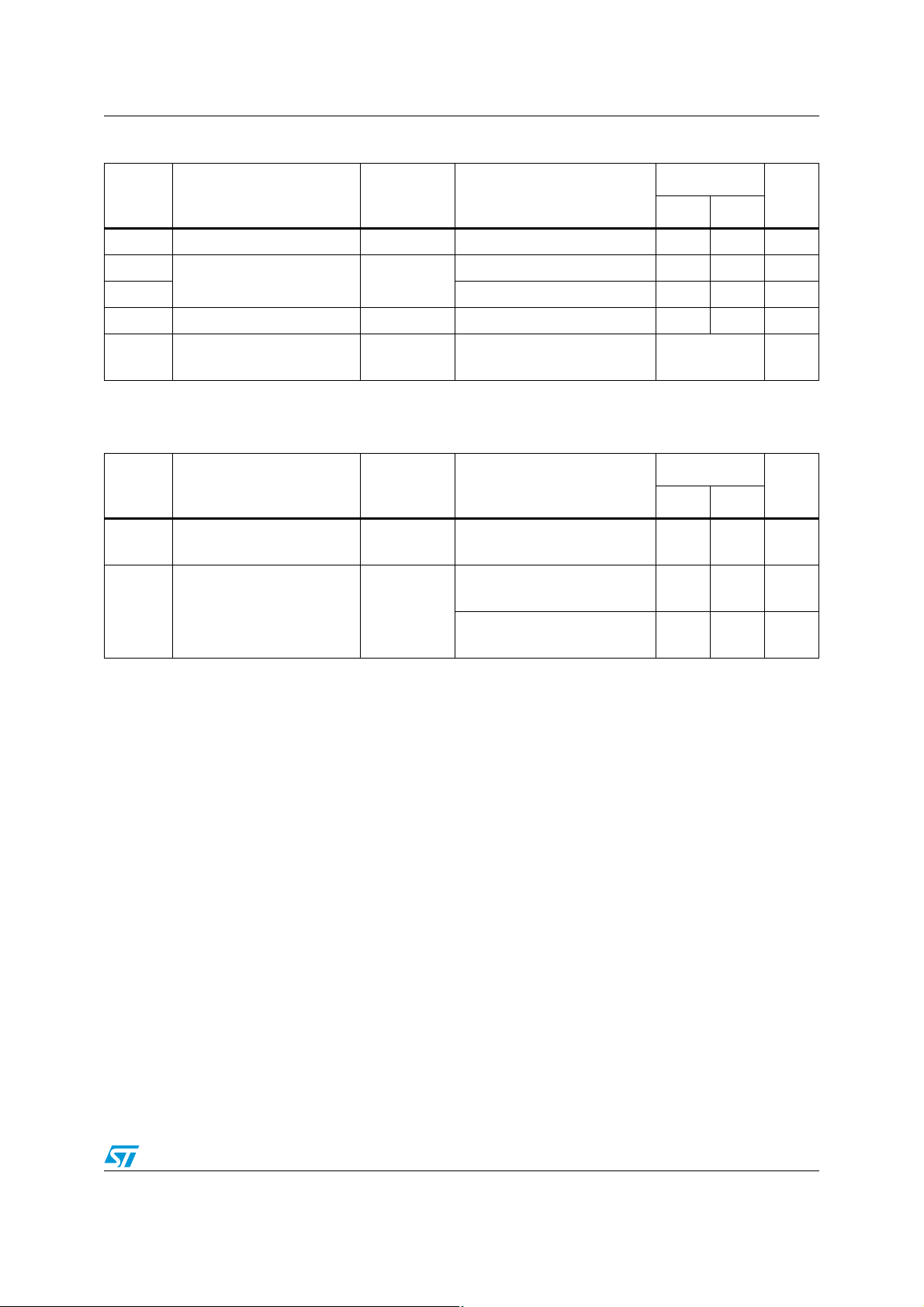
Table 4. Electrical measurements at ambiant temperature (per diode), T
Symbol Characteristic
I
R
(1)
V
F1
(1)
V
F2
C Capacitance 4001 V
Z
th(j-c)
1. Pulse width ≤ 680µs, Duty Cycle ≤ 2%
Table 5. Electrical measurements at high and low temperatures (per diode)
Symbol Characteristic
I
R
(1)
V
F2
1. Pulse width ≤ 680µs, Duty Cycle ≤ 2%
s
MIL-STD-750
test method
Test conditions
amb
Reverse Current 4016 DC method, VR = 100 V - 30 µA
Forward Voltage 4011
Pulse method, I
= 10 A - 780 mV
F
Pulse method, IF = 20 A - 1 V
= 10 V, F = 1 MHz - 700 pF
R
= 15 to 40 A, tH = 50 ms
Relative thermal impedance,
junction to case
3101
MIL-STD-750
test method
Reverse Current 4016
Forward Voltage 4011
I
H
= 50 mA, tmd = 100 µs
I
M
Test conditions
T
= +125 (+0, -5) °C
case
DC method, V
T
= +125 (+0, -5) °C
case
pulse method, I
T
= -55 (+5, -0) °C
case
pulse method, I
= 100 V
R
= 20 A
F
= 20 A
F
= 22 ±3 °C
Values
Units
Min. Max.
Calculate ΔV
Values
Min. Max.
-20mA
-900mV
-1.1V
°C/W
F
Units
Doc ID 16953 Rev 1 3/10
Page 4
Configurations STPS20100HR
2 Configurations
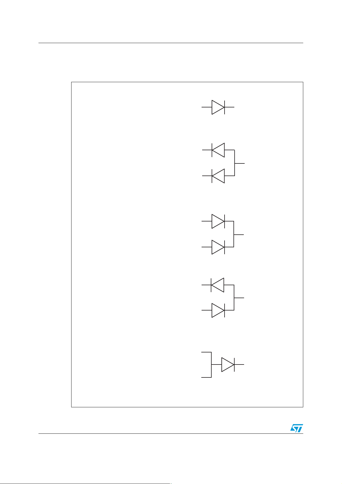
Figure 1. Available device configurations
Variant 01
Terminal 1:
Terminal 2:
Terminal 3:
Terminal 1:
Terminal 2:
Terminal 3:
Cathode
No connection
Anode
Cathode a
Common anode
Cathode b
STPS20100FSYHRB
3
Variant 02
STPS20100AFSY1
STPS20100AFSYHRB
1
3
Variant 03
STPS20100CFSY1
STPS20100CFSYHRB
1
2
Terminal 1:
Terminal 2:
Terminal 3:
Terminal 1:
Terminal 2:
Terminal 3:
Terminal 1:
Terminal 2:
Terminal 3:
Anode a
Common cathode
Anode b
STPS20100SFSYHRB
Anode a
Center tap
Cathode b
Anode
Anode
Cathode
1
2
3
Variant 04
3
2
1
Variant 05
STPS20100S1
STPS20100SHRB
1
3
2
For TO-254 the case is not connected to any lead
For SMD.5 the lid is not connected to any terminal
4/10 Doc ID 16953 Rev 1
Page 5
STPS20100HR Package Information
3 Package Information
In order to meet environmental requirements, ST offers these devices in different grades of
ECOPACK
specifications, grade definitions and product status are available at: www.st.com.
ECOPACK
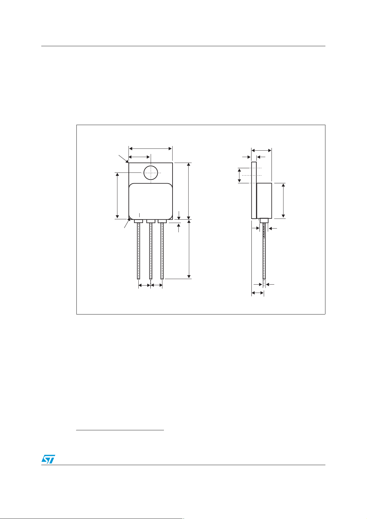
Figure 2. Metal flange mount package (TO-254
®
packages, depending on their level of environmental compliance. ECOPACK®
®
is an ST trademark.
(a)
), 3 lead dimension definitions
R1
G
R2
B
H
ØF
C
3
2
1
N
L
D
E
A
ØM
K
K
a. The terminal identification is specified by the device configuration. See Figure 1 for terminal connections
ØI
J
Doc ID 16953 Rev 1 5/10
Page 6

Package Information STPS20100HR
Table 6. Metal flange mount package (TO-254), 3-lead dimension values
Dimension in millimetres Dimlension in inches
Reference
Min. Max. Min. Max.
A 13.59 13.84 0.535 0.545
B 13.59 13.84 0.535 0.545
C 20.07 20.32 0.790 0.800
D 6.3 6.7 0.248 0.264
E 1 3.9 0.039 0.154
ØF 3.5 3.9 0.138 0.154
G 16.89 17.4 0.665 0.685
H 6.86 BSC 0.270 BSC
(1)
ØI
J 3.81 BSC 0.150 BSC
K 3.81 BSC 0.150 BSC
L 12.95 14.5 0.510 0.571
ØM 3.05 Typ. 0.120 Typ.
N - 0.71 - 0.028
(2)
R1
(3)
R2
1. 3 locations
2. Radius of heatsink flange corner - 4 locations
3. Radius of body corner - 4 locations
0.89 1.14 0.035 0.045
- 1 - 0.039
1.65 Typ. 0.065
6/10 Doc ID 16953 Rev 1
Page 7
STPS20100HR Package Information
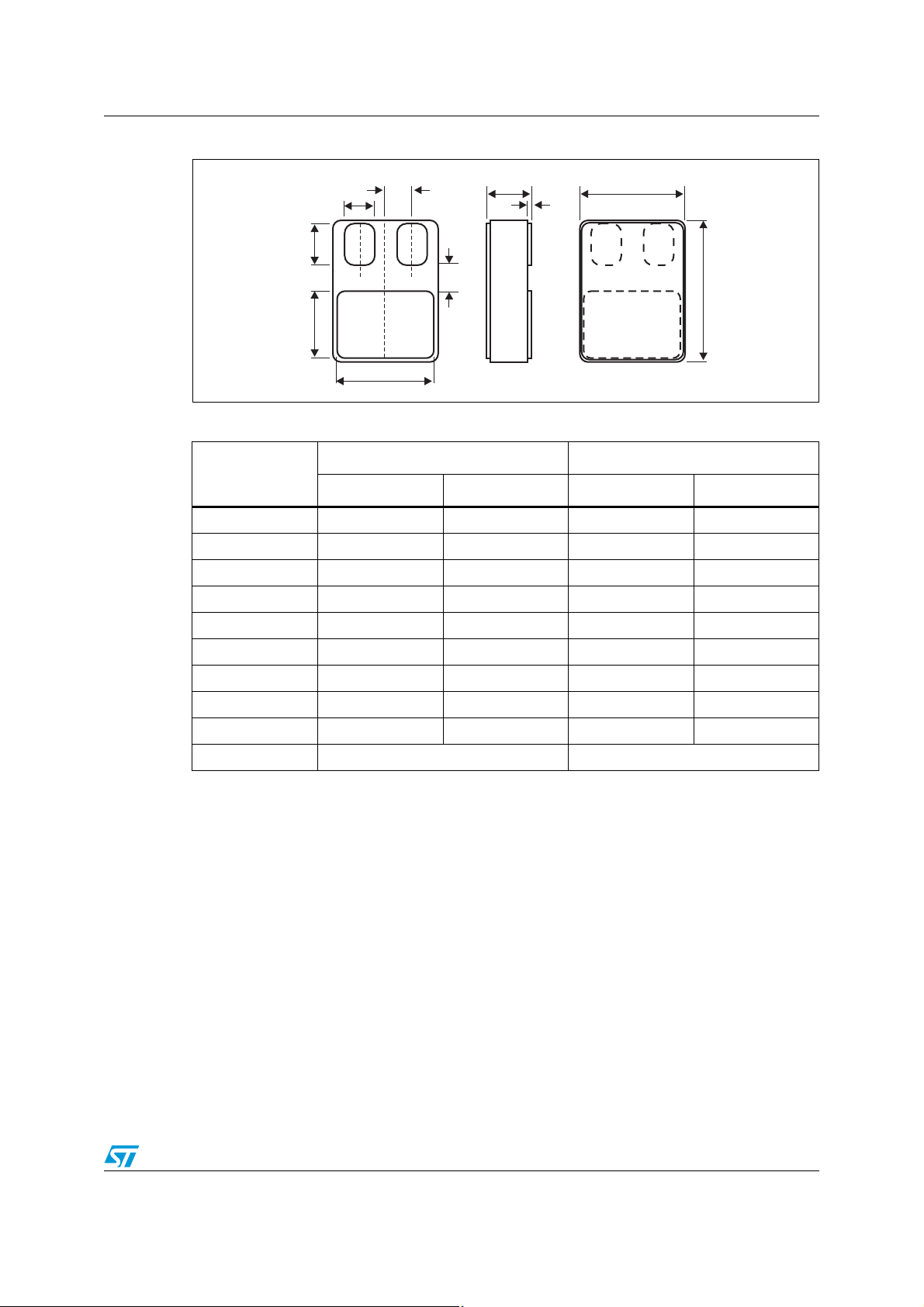
Figure 3. Surface mount package (SMD.5), 3-terminal dimension definitions
A
A1
E
b3
b2
e
2
1
D1
D
b1
3
b
Table 7. Surface mount package (SMD.5), 3-terminal dimension values
Dimension in millimetres Dimlension in inches
Reference
Min. Max. Min. Max.
A 2.84 3.15 0.112 0.124
A1 0.25 0.51 0.010 0.20
b 7.13 7.39 0.281 0.291
b1 5.58 5.84 0.220 0.230
(1)
b2
b3
(1)
2.28 2.54 0.090 0.100
2.92 3.18 0.115 0.125
D 10.03 10.28 0.395 0.405
(1)
D1
E 7.39 7.64 0.291 0.301
(1)
e
1. 2 locations
0.76 - 0.030 -
1.91 BSC 0.075
Doc ID 16953 Rev 1 7/10
Page 8
Ordering Information STPS20100HR
4 Ordering Information
Table 8. Ordering information
Order code
STPS20100S1 -
STPS20100SHRB 5106/016/05 Gold 510601605 -
STPS20100FSYHRB 5106/016/01
STPS20100AFSY1 - Gold
STPS20100AFSYHRB 5106/016/02 Solder dip 510601602 + BeO Y
STPS20100CFSY1 - Gold
STPS20100CFSYHRB 5106/016/03 Solder dip 510601603 + BeO Y
STPS20100SFSYHRB 5106/016/04 Solder dip 510601604 + BeO Y
ESCC detailed
specification
Package Lead finish Marking EPPL
Gold STPS20100S1 -
SMD.5
Solder dip 510601601 + BeO -
STPS20100AFSY1
+ BeO
TO-254
STPS20100CFSY1
+ BeO
Mass
-
10.0
-
(g)
2.0
Packing
Waffle
pack
8/10 Doc ID 16953 Rev 1
Page 9

STPS20100HR Revision history
5 Revision history
Table 9. Document revision history
Date Revision Changes
25-Mar-2010 1 Initial release.
Doc ID 16953 Rev 1 9/10
Page 10

STPS20100HR
Please Read Carefully:
Information in this document is provided solely in connection with ST products. STMicroelectronics NV and its subsidiaries (“ST”) reserve the
right to make changes, corrections, modifications or improvements, to this document, and the products and services described herein at any
time, without notice.
All ST products are sold pursuant to ST’s terms and conditions of sale.
Purchasers are solely responsible for the choice, selection and use of the ST products and services described herein, and ST assumes no
liability whatsoever relating to the choice, selection or use of the ST products and services described herein.
No license, express or implied, by estoppel or otherwise, to any intellectual property rights is granted under this document. If any part of this
document refers to any third party products or services it shall not be deemed a license grant by ST for the use of such third party products
or services, or any intellectual property contained therein or considered as a warranty covering the use in any manner whatsoever of such
third party products or services or any intellectual property contained therein.
UNLESS OTHERWISE SET FORTH IN ST’S TERMS AND CONDITIONS OF SALE ST DISCLAIMS ANY EXPRESS OR IMPLIED
WARRANTY WITH RESPECT TO THE USE AND/OR SALE OF ST PRODUCTS INCLUDING WITHOUT LIMITATION IMPLIED
WARRANTIES OF MERCHANTABILITY, FITNESS FOR A PARTICULAR PURPOSE (AND THEIR EQUIVALENTS UNDER THE LAWS
OF ANY JURISDICTION), OR INFRINGEMENT OF ANY PATENT, COPYRIGHT OR OTHER INTELLECTUAL PROPERTY RIGHT.
UNLESS EXPRESSLY APPROVED IN WRITING BY AN AUTHORIZED ST REPRESENTATIVE, ST PRODUCTS ARE NOT
RECOMMENDED, AUTHORIZED OR WARRANTED FOR USE IN MILITARY, AIR CRAFT, SPACE, LIFE SAVING, OR LIFE SUSTAINING
APPLICATIONS, NOR IN PRODUCTS OR SYSTEMS WHERE FAILURE OR MALFUNCTION MAY RESULT IN PERSONAL INJURY,
DEATH, OR SEVERE PROPERTY OR ENVIRONMENTAL DAMAGE. ST PRODUCTS WHICH ARE NOT SPECIFIED AS "AUTOMOTIVE
GRADE" MAY ONLY BE USED IN AUTOMOTIVE APPLICATIONS AT USER’S OWN RISK.
Resale of ST products with provisions different from the statements and/or technical features set forth in this document shall immediately void
any warranty granted by ST for the ST product or service described herein and shall not create or extend in any manner whatsoever, any
liability of ST.
ST and the ST logo are trademarks or registered trademarks of ST in various countries.
Information in this document supersedes and replaces all information previously supplied.
The ST logo is a registered trademark of STMicroelectronics. All other names are the property of their respective owners.
© 2010 STMicroelectronics - All rights reserved
STMicroelectronics group of companies
Australia - Belgium - Brazil - Canada - China - Czech Republic - Finland - France - Germany - Hong Kong - India - Israel - Italy - Japan -
Malaysia - Malta - Morocco - Philippines - Singapore - Spain - Sweden - Switzerland - United Kingdom - United States of America
www.st.com
10/10 Doc ID 16953 Rev 1
 Loading...