


STODD01
Monolithic power management for high definition ODD with true
shut-down, reset, and programmable step-up voltage
Features
■ 1.2 MHz DC-DC current mode PWM converter
■ Dual step-down of up to 800 mA
■ Single step-up of up to 700 mA
■ 2 % DC output voltage tolerance for step-down
■ 3 % DC output voltage tolerance for step-up
■ Programmable step-up output voltage by S-
WIRE
■
Synchronous rectification
■ Power save mode at light load for step-down
■ Typical efficiency: > 90 %
■ Internal soft start with controlled inrush current
■ Reset function
■ Enable function for step-up
■ True cut-off function for step-up
■ Low switching quiescent current: max 2.2 mA
overtemperature range
■ Uses tiny capacitors and inductors
■ Available in QFN16 (4 x 4 mm.)
Description
The STODD01 is a complete power management
for Blu-Ray, based on high density optical storage
devices. It integrates two step-down converters
and one step-up. The step-down converters are
optimized for powering low-voltage digital core, up
to 0.8 A, in ODD applications and, generally, to
replace the high current linear solution when
power dissipation may cause a high heating of the
application environment. The step-up provides
the necessary voltage to supply the blue laser in
mobile applications where only 5 V is available.
The output voltage is programmable by using the
Table 1. Device summary
S-Wire protocol, in the range of 6.5 V to 14 V, with
a current capability of 0.7 A. The integrated low
R
for N-channel and P-channel MOSFET
DSon
switches contribute to obtaining high efficiency.
The enable function for the step-up section, and
reset function for monitoring the input voltage,
make the device particularly suitable for optical
storage applications. The high switching
frequency (1.2 MHz typ.) allows the use of tiny
surface mounted components. Furthermore, a low
output ripple is achieved by the current mode
PWM topology and by the use of X7R or X5R low
ESR SMD ceramic capacitors. The device
includes soft-start control, thermal shutdown, and
peak current limit, to prevent damage due to
accidental overload. The STODD01 is packaged
in QFN16 (4 x 4 mm.).
QFN16L (4 x 4 mm.)
Part number Order code Marking Package
STODD01 STODD01PQR ODD01 QFN16 (4 x 4 mm.)
February 2011 Doc ID 17789 Rev 2 1/31
www.st.com
31

Contents STODD01
Contents
1 Block diagram . . . . . . . . . . . . . . . . . . . . . . . . . . . . . . . . . . . . . . . . . . . . . . 3
2 Absolute maximum ratings . . . . . . . . . . . . . . . . . . . . . . . . . . . . . . . . . . . 4
3 Pin configuration . . . . . . . . . . . . . . . . . . . . . . . . . . . . . . . . . . . . . . . . . . . . 5
4 Typical application . . . . . . . . . . . . . . . . . . . . . . . . . . . . . . . . . . . . . . . . . . 6
5 Electrical characteristics . . . . . . . . . . . . . . . . . . . . . . . . . . . . . . . . . . . . . 7
6 S-wire protocol . . . . . . . . . . . . . . . . . . . . . . . . . . . . . . . . . . . . . . . . . . . . 10
7 Detailed description . . . . . . . . . . . . . . . . . . . . . . . . . . . . . . . . . . . . . . . . 14
7.1 Brief overview . . . . . . . . . . . . . . . . . . . . . . . . . . . . . . . . . . . . . . . . . . . . . . 14
7.2 Enable pin . . . . . . . . . . . . . . . . . . . . . . . . . . . . . . . . . . . . . . . . . . . . . . . . 14
7.3 TX pin . . . . . . . . . . . . . . . . . . . . . . . . . . . . . . . . . . . . . . . . . . . . . . . . . . . . 15
7.4 Reset function . . . . . . . . . . . . . . . . . . . . . . . . . . . . . . . . . . . . . . . . . . . . . 15
7.5 Overtemperature protection . . . . . . . . . . . . . . . . . . . . . . . . . . . . . . . . . . . 16
7.6 Overvoltage protection . . . . . . . . . . . . . . . . . . . . . . . . . . . . . . . . . . . . . . . 16
8 Typical performance characteristics . . . . . . . . . . . . . . . . . . . . . . . . . . . 17
9 Application information . . . . . . . . . . . . . . . . . . . . . . . . . . . . . . . . . . . . . 21
9.1 Introduction . . . . . . . . . . . . . . . . . . . . . . . . . . . . . . . . . . . . . . . . . . . . . . . 21
9.2 Programming the output voltage . . . . . . . . . . . . . . . . . . . . . . . . . . . . . . . 21
9.3 Inductor selection . . . . . . . . . . . . . . . . . . . . . . . . . . . . . . . . . . . . . . . . . . . 21
9.4 Input and output capacitor selection . . . . . . . . . . . . . . . . . . . . . . . . . . . . . 22
9.5 Layout considerations . . . . . . . . . . . . . . . . . . . . . . . . . . . . . . . . . . . . . . . . 23
10 Recommended PCB layout . . . . . . . . . . . . . . . . . . . . . . . . . . . . . . . . . . 24
11 Package mechanical data . . . . . . . . . . . . . . . . . . . . . . . . . . . . . . . . . . . . 26
12 Revision history . . . . . . . . . . . . . . . . . . . . . . . . . . . . . . . . . . . . . . . . . . . 30
2/31 Doc ID 17789 Rev 2

STODD01 Block diagram
1 Block diagram
Figure 1. STODD01 block diagram
SW1
SW1
EN
EN
V
V
IN_A
IN_A
V
V
IN_P
IN_P
Reset
Reset
TX
TX
S-Wire
S-Wire
Reset
Reset
Step-Up 700mA
Step-Up 700mA
ch1
ch1
Step-Down
Step-Down
800mA
800mA
ch2
ch2
Step-Down
Step-Down
800mA
800mA
ch3
ch3
Out1
Out1
FB1
FB1
SW2
SW2
FB2
FB2
SW3
SW3
FB3
FB3
GND GND
GND GND
GND GND
GND GND
Doc ID 17789 Rev 2 3/31

Absolute maximum ratings STODD01
2 Absolute maximum ratings
Table 2. Absolute maximum ratings
Symbol Parameter Value Unit
V
V
IN_A
IN_P
Analog input voltage - 0.3 to 7 V
Power input voltage - 0.3 to 7 V
EN Enable voltage - 0.3 to 7 V
SW1 Switch pin for ch1 - 0.3 to 16 V
SW2,SW3 Switch pin for ch2 and ch3 - 0.3 to 7 V
OUT1 Output voltage for ch1 - 0.3 to 16 V
FB1 Feedback pin for ch1 - 0.3 to 2.5 V
FB2 Feedback pin for ch2 - 0.3 to 5 V
FB3 Feedback pin for ch3 - 0.3 to 2.5 V
Reset Reset pin - 0.3 to V
+ 0.3 V
IN
TX S-wire pin - 0.3 to 7 V
T
T
T
J
STG
JOP
Maximum junction temperature 150 °C
Storage temperature range - 65 to + 150 °C
Operating junction temperature range - 25 to + 125 °C
Note: Absolute maximum ratings are those values beyond which damage to the device may occur.
Functional operation under these conditions is not implied.
Table 3. Thermal data
Symbol Parameter Value Unit
R
R
thJC
thJA
Thermal resistance junction-case 2.5 °C/W
Thermal resistance junction-ambient 46 °C/W
Table 4. ESD
Symbol Parameter Value Unit
HBM Human body model 2 kV
MM Machine model 200 V
4/31 Doc ID 17789 Rev 2

STODD01 Pin configuration
3 Pin configuration
Figure 2. Pin connection (top through view)
Table 5. Pin description
Pin n° Symbol Name and function
1 GND_P Power Ground pin (ch1)
2 FB1 Step-up feedback pin (ch1)
3V
IN_A
Power Supply for internal analog circuits
4 FB2 Step-down feedback pin (ch2)
5 GND_P Power Ground pin (ch2)
6 SW2 Step-down switching pin (ch2)
7V
IN_P
Power input voltage pin
8 SW3 Step-down switching pin (ch3)
9 GND_P Power Ground pin (ch3)
10 FB3 Step-down feedback pin (ch3)
11 GND_A Analog Ground pin
12 OUT1 Step-up output voltage
13 TX S-Wire pin. If connected to GND, V
FB1
=0.8V
(1)
14 SW1 Step-up switching pin (ch1)
Enable pin. Connecting the pin to a voltage higher than 1.2 V the step-up is
15 EN
ON.Connecting the pin to a voltage lower than 0.4 V the step-up is OFF,
resulting in no current flow to the load
16 Reset Reset pin. It is an open drain output
Exposed pad Ground and thermal dissipation pad
1. If this function is not used, the TX pin must be connected to GND
Doc ID 17789 Rev 2 5/31

Typical application STODD01
4 Typical application
Figure 3. Application circuit
L1
L1
C1
V
V
IN
IN
C3
C3
C2
C2
Reset
Reset
EN
EN
TX
TX
C1
R5
R5
V
V
IN_A
IN_A
V
V
IN_P
IN_P
Reset
Reset
EN
EN
TX
TX
GND
GND
SW1
SW1
STODD01
STODD01
GNDGND
GNDGND
Out1
Out1
FB1
FB1
SW2
SW2
FB2
FB2
SW3
SW3
FB3
FB3
GND
GND
R1
R1
R2
R2
L2
L2
L3
L3
R3
R3
R4
R4
C4
C4
C5
C5
C6
C6
V
V
V
V
V
V
OUT1
OUT1
OUT2
OUT2
OUT3
OUT3
Note: If the S-wire function is not used, the TX pin must be connected to GND.
Table 6. List of external components
Component Manufacturer Part number Value Size
C1, C2, C3 Murata GRM21BR61A106KE19L 10 µF 0805
C4, C5, C6 Murata GRM32ER61C226KE20L 22 µF 1210
L1 Coilcraft LPS6225-472MLB 4.7 µH 6 x 6 x 2.5
L2, L3 Coilcraft LPS4018-332MLB 3.3 µH 4.1 x 4.1 x 1.8
R1 33 kΩ (V
R2 3.3 kΩ 0603
R3 27 kΩ (V
R4 47 kΩ 0603
R5 100 kΩ
1. The components listed above refer to typical applications. Operation of the STODD01 is not limited to the choice of these
external components.
2. R1 and R2 are calculated according to the following formula:
R1 = R2 x (V
OUT1/VFB1
3. R3 and R4 are calculated according to the following formula:
R3 = R4 x (V
OUT3/VFB3
4. It is recommended to use resistors with values in the range of 100kΩ to 1MΩ.
- 1). It is recommended to use resistors with values in the range of 1 kΩ to 50 kΩ.
- 1). It is recommended to use resistors with values in the range of 1 kΩ to 50 kΩ.
(1)
OUT1
OUT3
= 8.8 V)
= 1.2 V)
(2)
(3)
(4)
0603
0603
0603
6/31 Doc ID 17789 Rev 2

STODD01 Electrical characteristics
5 Electrical characteristics
V
= V
IN_P
C
= 22 µF, L1 = 4.7 µH, L2 = L3 = 3.3 µH, TJ = - 25 to 125 °C (unless otherwise
4,5,6
specified; typical values are referred to T
Table 7. Electrical characteristics
Symbol Parameter Test conditions Min. Typ. Max. Unit
= VEN = 5 V, V
IN_A
OUT1
= 9 V, V
= 3.3 V, V
OUT2
= 25 °C).
J
OUT3
= 1.2 V, C
1,2,3
= 10 µF,
V
IN
I
SUPPLY
Step-up section
V
OUT
V
FB1
I
FB1
I
OUT1_OFF
(leak)
V
OVP Overvoltage protection
OUT1
R
DSon_N
R
DSon_P
I
SW1 (leak)
I
SW1 (LIM)
PWM f
s
D
MAX
ν Efficiency
V
EN_H
V
EN_L
I
EN
ΔV
/ΔVINLine transient response
OUT1
ΔV
/ΔI
OUT1
OUT
ΔV
/ΔVINStartup transient
OUT1
Input voltage range 4 6 V
V
> 1.2 V, No Switching 1.6 2.2 mA
Supply current
EN
V
< 0.4 V, No Switching 1.2 2.0 mA
EN
Output voltage range 6.5 14 V
Prog. feedback voltage
range
I
= 50 mA (prog. by S-Wire
OUT1
see Figure 9 and Ta b le 9 )
0.776 0.8 0.824 V
Feedback voltage accuracy -3 3 %
Feedback current V
= 0 V, VEN= 2 V 600 nA
FB1
Output leakage current VEN= 0 V, TJ = -25 to 80 °C 20 µA
(1)
V
= 0 V 14.8 15.3 15.8 V
FB1
Internal N-channel R
Internal P-channel R
DSon
DSon
Internal leakage current V
SW Current limitation V
Oscillator frequency to be measured on t
Max duty cycle on SW1 pin, V
Enable threshold high V
Enable threshold low V
Enable pin current V
Load transient response
(2)
I
=400 mA 300
SW1
I
=400 mA 300
SW1
SW1
OUT1
I
OUT1
I
OUT1
I
OUT1
I
OUT1
=4 to 6 V, I
IN
= 4 to 6 V, I
IN
= VIN = 5 V 2 µA
EN
VIN from 4 to 6 V, I
(2)
mA, t
V
(2)
= 5 V, I
IN
= 4 V, V
= 9.2 V 2.6 A
=50 mA, V
=700 mA, V
=100 mA, V
=700 mA, V
= tF => 30 µs, TJ=25 °C
R
= 2 V, VEN= 0 V 2 µA
FB1
= 0.7 V 70 90 %
FB1
OUT1
OUT1
OUT1
OUT1
OUT1
OUT1
OUT1
from 100 mA to
OUT1
500 mA, tR = tF => 5µs, TJ=25 °C
V
from 0 to 5 V, I
IN
OUT1
pin 0.75 1.2 1.5 MHz
SW1
=7 V 80 %
=7 V 90 %
=9 V 75 %
=9 V 90 %
= 50 mA 1.2
= 50 mA 0.4
= 500
-5 5
-5 5
= 500 mA -10 10
V
V
V
mΩ
V
%
OUT
%
OUT
%
OUT
Doc ID 17789 Rev 2 7/31

Electrical characteristics STODD01
Table 7. Electrical characteristics (continued)
Symbol Parameter Test conditions Min. Typ. Max. Unit
t
START
Startup time VEN from 0 to 5 V, I
Inrush current V
Step-down section
%V
%V
ΔV
I
ΔV
OUT2,3
FB
2
I
FB2
FB
3
I
FB3
I
OUT2,3
OUT_MIN
OUT2,3
PWM f
OUT2
OUT3
D
MAX
I
SWL
I
LKP2,3
I
LKN2,3
R
DSon-N
R
DSon-P
T2,3
Feedback voltage 3.23 3.3 3.37 V
FB2 Pin bias current V
Feedback voltage 0.784 0.8 0.816 mV
FB3 Pin bias current V
Output current
Minimum output current 0 mA
Reference load regulation 10 mA < I
PWM Switching frequency I
S
/ΔVINLine regulation 4 V < V
/ΔVINLine regulation 4 V < V
Maximum duty cycle V
Switching current limitation 1.5 A
PMOS Leakage current
NMOS Leakage current
NMOS Switch on resistance ISW = 250 mA 0.2 0.4 W
PMOS Switch on resistance ISW = 250 mA 0.3 0.5 W
/ΔI
OU
Load transient response
ν Efficiency V
ν Efficiency V
Reset section
OUT3
OUT2
(3)
= 1.2 V
= 3.3 V
=100 mA 500 µs
OUT1
=9.25 V, I
OUT
= 3.5 V 15 20 µA
FB2
= 1 V 600 nA
FB3
=100 mA 1.3 A
OUT
VIN = 4 to 6 V 700 800 mA
< 0.8 A 5.5 15 mV
OUT2,3
= 0.3 A 1.2 MHz
OUT2,3
< 6 V 0.032
IN
< 6 V 0.15
IN
(2)
= 3.0 V, V
FB2
= 3.5 V, V
V
FB2
= GND, TJ=- 25 to 80 °C
V
SW2,3
= 3.5 V, V
V
FB2
V
= 5 V, TJ =- 25 to 80 °C
SW2,3
100 mA < I
=> 100 ns, TJ = 25 °C
t
F
I
OUT3
I
OUT3
I
OUT2
I
OUT2
OUT2,3
= 100 mA 65
= 800 mA 80
= 100 mA 75
= 800 mA 90
= 0.7 V
FB3
= 0.9 V,
FB3
= 0.9 V,
FB3
< 500 mA, tR =
85 94 %
0.1 µA
0.1 µA
-5 +5
V
V
V
%
OUT
/V
%
OUT
/V
%
OUT
%
%
IN
IN
t
V
DEL
R_TH
Delay time TJ = 25 °C 100 ms
V
Rising (see Figure 12 and
IN
Figure 29) (measured on input
voltage pin)
Reset threshold
V
Falling (see Figure 12 and
IN
V
R_TL
Figure 29) (measured on input
voltage pin)
8/31 Doc ID 17789 Rev 2
4.3 4.4
V
4.1 4.2

STODD01 Electrical characteristics
Table 7. Electrical characteristics (continued)
Symbol Parameter Test conditions Min. Typ. Max. Unit
V
RL
I
RH
Reset output voltage low
Reset leakage current
V
output
V
°C
Thermal section
T
SHDN
T
HYS
1. If V
OUT1
2. Guaranteed by design, but not tested in production.
3. V
= 90 % of nominal value
OUT
Thermal shutdown
Thermal shutdown
hysteresis
> OVP voltage the device stops to switch.
(2)
(2)
=4 V, I
IN
=5 V, V
IN
=6 mA open drain
SINK
=5 V, TJ=-25 to 80
RES
0.4 V
5 200 nA
130 150 °C
15 °C
Doc ID 17789 Rev 2 9/31

S-wire protocol STODD01
6 S-wire protocol
Table 8. Timing
Parameter Symbol Min. Typ. Max. Unit
S-Wire signal start (see Figure 5, 6, 7, 8)t
S-Wire signal stop (see Figure 5, 6, 7, 8)t
S-Wire signal off (see Figure 5, 6, 7, 8)t
S-Wire high (see Figure 5, 6, 7, 8)t
S-Wire low (see Figure 5, 6, 7, 8)t
S-Wire rising time (see Figure 4)t
S-Wire falling time (see Figure 4)t
FB Voltage delay t
S-Wire threshold high (see Figure 4)V
S-Wire threshold low (see Figure 4)V
SW_START
SW_STOP
SW_OFF
SW_H
SW_L
SW_R
SW_F
SW_DELAY
SW_TH
SW_TL
300 500 µs
300 500 µs
270 µs
25 50 µs
25 50 µs
200 ns
200 ns
20 µs
1.6 V
00.4V
IN
Note: These are recommended values for proper operation of the S-wire interface.
The S-wire input pin is able to detect pulses also outside these ranges. Consequently, care
must be taken to avoid noise injected into the S-wire pin.
Figure 4. S-wire pulse thresholds
AM07818v1
AM07818v1
V
V
V
SW_TH
SW_TH
V
V
SW_TL
SW_TL
90%
90%
10%
10%
T
T
SW_R
SW_R
10/31 Doc ID 17789 Rev 2
T
T
SW_F
SW_F

STODD01 S-wire protocol
Figure 5. S-wire protocol timing diagrams (case a)
5 V
5 V
V
V
V
V
IN
IN
IN
IN
GND
GND
5 V
5 V
EN
EN
EN
EN
GND
GND
-
-
S-Wire
S-Wire
S-Wire
GND
GND
GND
GND
GND
GND
S-Wire
V
V
V
V
FB1
FB1
FB1
FB1
V
V
V
V
OUT1
OUT1
OUT1
OUT1
t
t
SW_START
SW_START
0.8 V
0.8 V
9 V
9 V
SET BY RESISTOR DIVIDER
SET BY RESISTOR DIVIDER
t
t
t
t
SW_H
SW_H
2 3 41
2 3 41
2 3 41
2 3 41
t
t
t
t
SW_L
SW_L
t
t
SW_STOP
SW_STOP
0.86 V
0.86 V
9.675 V
9.675 V
0.86 V
0.86 V
9.675 V
9.675 V
t
t
SW_START
SW_START
Figure 6. S-wire protocol timing diagrams (case b)
5V
5V
5V
V
V
V
IN
IN
IN
GND
GND
GND
EN
EN
EN
GND
GND
GND
S-Wire
S-Wire
GND
GND
GND
GND
GND
GND
GND
GND
GND
S-Wire
V
V
V
FB1
FB1
FB1
V
V
V
OUT1
OUT1
OUT1
t
t
t
SW_START
SW_START
SW_START
t
t
t
SW_H
SW_H
SW_H
2 3 41
2 3 41
22 33 4411
t
t
t
SW_L
SW_L
SW_L
t
t
t
SW_STOP
SW_STOP
SW_STOP
t
t
SW_DELAY
SW_DELAY
5V
5V
5V
0.86V
0.86V
0.86V
9.675V
9.675V
9.675V
t
t
SW_START
SW_START
0.86V
0.86V
0.86V
9.675V
9.675V
9.675V
t
t
t
SW_START
SW_START
SW_START
Doc ID 17789 Rev 2 11/31

S-wire protocol STODD01
Figure 7. S-wire protocol timing diagrams (case c)
5V
5V
5V
5V
t
t
SW_START
SW_START
t
t
SW_H
0.8V
0.8V
9V
9V
SET BY RESISTOR DIVIDER
SET BY RESISTOR DIVIDER
SW_H
2 3 41
22 33 4411
t
t
SW_L
SW_L
t
t
SW_STOP
SW_STOP
0.86V
0.86V
9.675V
9.675V
21
2211
t
t
SW_STOP
SW_STOP
0.83V
0.83V
9.338V
9.338V
t
t
SW_OFF
SW_OFF
0.8V
0.8V
9V
9V
GND
GND
GND
GND
GND
GND
GND
GND
GND
GND
V
V
IN
IN
EN
EN
S-Wire
S-Wire
V
V
FB1
FB1
V
V
OUT1
OUT1
t
t
t
SW_START
SW_START
Figure 8. S-wire protocol timing diagrams (case d)
5V
5V
V
V
IN
IN
GND
GND
GND
GND
GND
GND
GND
GND
GND
GND
EN
EN
S-Wire
S-Wire
V
V
FB1
FB1
V
V
OUT1
OUT1
5V
5V
t
t
SW_START
SW_START
t
t
SW_H
0.8V
0.8V
9V
9V
SET BY RESISTOR DIVIDER
SET BY RESISTOR DIVIDER
SW_H
2 3 41
22 33 4411
t
t
SW_L
SW_L
t
t
t
SW_STOP
SW_STOP
SW_DELAY
SW_DELAY
0.86V
0.86V
9.675V
9.675V
t
t
SW_OFF
SW_OFF
0.8V
0.8V
0.9V
0.9V
t
t
SW_START
SW_START
1
11
2
22
t
t
SW_STOP
SW_STOP
0.83V
0.83V
9.338V
9.338V
t
t
Sw_START
Sw_START
t
t
SW_DELAY
SW_DELAY
12/31 Doc ID 17789 Rev 2

STODD01 S-wire protocol
Table 9. Feedback one voltage level
S-Wire pulses V
(V) S-Wire pulses V
FB1
(V) S-Wire pulses V
FB1
FB1
0 (Default value) 0.800 11 0.965 22 1.130
1 0.815 12 0.980 23 1.145
2 0.830 13 0.995 24 1.160
3 0.845 14 1.010 25 1.175
4 0.860 15 1.025 26 1.190
5 0.875 16 1.040 27 1.205
6 0.890 17 1.055 28 1.220
7 0.905 18 1.070 29 1.235
8 0.920 19 1.085 30 1.250
9 0.935 20 1.100
10 0.950 21 1.115
Figure 9. Single wire programming
S-Wire
S-Wire
V
=0.8V (default value)
V
=0.8V (default value)
FB1
FB1
(V)
S-Wire
S-Wire
S-Wire
S-Wire
S-Wire
S-Wire
S-Wire
S-Wire
S-Wire
S-Wire
S-Wire
S-Wire
S-Wire
S-Wire
S-Wire
S-Wire
S-Wire
S-Wire
V
=0.8V
V
=0.8V
FB1
FB1
V
=0.815V
V
1
1
12
12
1
1
1234
1234
12345
12345
12345
12345
12345
12345
12345 26 28 29 3027
12345 26 28 29 3027
=0.815V
FB1
FB1
V
=0.830V
V
=0.830V
FB1
FB1
V
=0.845V
V
3
3
2
2
=0.845V
FB1
FB1
V
V
FB1
FB1
=0.860V
=0.860V
V
=0.875V
V
=0.875V
FB1
FB1
26 2827
26 2827
26 28 2927
26 28 2927
V
V
FB1
FB1
V
V
=1.22V
=1.22V
=1.235V
=1.235V
FB1
FB1
V
V
FB1
FB1
=1.25V
=1.25V
Doc ID 17789 Rev 2 13/31
Detailed description STODD01
7 Detailed description
7.1 Brief overview
The STODD01 is a complete high efficiency switching power management. Inside it has a
step-up converter with a current capability up to 0.7 A and two step-down converters with a
current capability up to 0.8 A.
The controller uses an average current mode technique in order to obtain good stability in all
application conditions.
The step-up converter, in order to guarantee the lowest switching ripple, operates in PWM
(pulse width modulation) in all load conditions.
Both step-down converters, in order to maintain good efficiency, operate in power-save
mode at light load. When the load increases, they automatically switch to PWM (pulse width
modulation) mode and the output voltage ripple is minimized.
The STODD01 is self protected against overtemperature and accidental short circuit in the
step down channel.
The soft-start function guarantees proper operation during startup.
7.2 Enable pin
The step-up section operates when the EN pin is set high. If the EN pin is set low the stepup turns OFF. In this condition the supply current is lower than 2 mA in the whole
temperature range, and it represents the consumption of the step-down section.
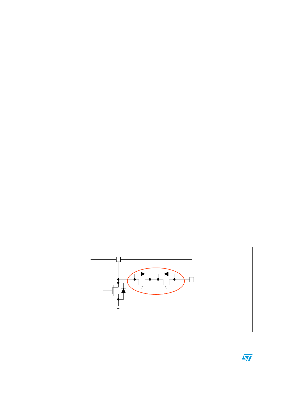
When the EN pin is low, thanks to at the true cut-off function, implemented using two Pchannel MOSFETs in a back-to-back configuration, as shown in Figure 10, the output
current is stopped. In order to control and reduce the in-rush current, the true cut-off Pchannel (P
Figure 10. True cut-off block
) manages the current during startup.
O
Ns
Ns
SW1
SW1
PGND
PGND
Ps
Ps
Po
Po
OUT1
OUT1
14/31 Doc ID 17789 Rev 2

STODD01 Detailed description
Figure 32 shows the in-rush current at enable transient. Initially, the C4 capacitor is
completely discharged and the current limitation is due only to the equivalent series resistor
of the inductor, the power MOSFET parasitic diode, and the cut-off MOSFETs’ R
DSon
. As
soon as the output voltage reaches the input voltage level, the device begins to switch and
the current is limited cycle by cycle.
The EN pin does not have an internal pull-up, which means that the enable pin cannot be
left floating.
If the enable function is not used, the EN pin must be connected to V
7.3 TX pin
The device implements an S-wire bus communication, which uses one control signal coming
from the microprocessor to program the step-up STODD01 output voltage (see Figure 11).
S-wire protocol allows the feedback voltage of the step-up section to be changed from 0.8 to
1.25 V, with steps of 15 mV (see Ta b le 9 ).
Figure 11. S-Wire connection
µP
GND
GND
Reset
EN
TX
Reset
EN
STODD01
TX
GND
GND
.
IN
This feature allows complete and easy control of the laser diode power during read and
write operation.
If this function is not used, the TX pin must be connected to GND.
7.4 Reset function
This flag shows that input voltage is in the correct range.
A comparator senses the input voltage. When it is higher than V
high impedance, with a delay of 100 ms (typ.). If it is below V
impedance (see Figure 12).
, the reset pin goes to
R_TH
, the reset pin goes to low
R_TL
Doc ID 17789 Rev 2 15/31

Detailed description STODD01
Figure 12. Reset function
V
V
R_TH
V
V
IN
IN
Reset
Reset
R_TH
t
t
DEL
DEL
V
V
R_TL
R_TL
The use of the reset function requires an external pull-up resistor which must be connected
between the reset pin and V
or any V
IN
voltage lower than 5 V. A pull-up resistor for reset
OUT
in the range of 100 kΩ to 1 MΩ is recommended.
If the reset function is not used, the reset pin may remain floating on the board.
7.5 Overtemperature protection
An internal temperature sensor continuously monitors the IC junction temperature. If the IC
temperature exceeds 150 °C (typ.) the device stops operating. As soon as the temperature
falls below 135 °C (typ.) normal operation is restored.
7.6 Overvoltage protection
The device provides overvoltage protection for monitoring the step-up output voltage.
If the sensed voltage on ch1 output exceeds 15.3 V (typ.) the step-up channel stops
switching. As soon as the output capacitor is discharged and the sensed voltage is below
14.8 V, it re-starts to switch (see Figure 13).
Figure 13. OVP function
OUTPU T Voltage
15.3V
14.8V
OVP sign al
Switching Switching
No Switching
16/31 Doc ID 17789 Rev 2

STODD01 Typical performance characteristics
8 Typical performance characteristics
C
= 10 µF, C
1,2,3
Figure 14. Supply current vs. temperature Figure 15. Feedback voltage vs. temperature
= 22 µF, L1 = 4.7 µH, L2 = L3 = 3.3 µH.
4,5,6
2.5
2
1.5
1
Supply Current [mA]
0.5
0
-40 -20 0 20 40 60 80 100 120 140
V
=5V, VEN<=0.4V, No Switching
IN_A=VIN_P
TEMPERATURE [°C]
Figure 16. Feedback voltage vs. temperature Figure 17. Feedback voltage vs. temperature
3.32
3.31
3.3
[V]
FB2
V
3.29
3.28
3.27
-40 -20 0 20 4 0 60 80 100 120 140
V
= V
= 5V, V
= 5V, I
IN_A
IN_P
EN
OUT2
= no load
TEMPERATURE [°C]
0.83
0.82
0.81
[V]
0.8
FB1
V
0.79
V
= V
= 5V, V
= 5V, I
IN_A
IN_P
0.78
0.77
-40 -20 0 20 40 60 80 100 120 140
EN
OUT1
= 50mA
TEMPERATURE [°C]
0.83
0.82
0.81
[V]
0.8
FB3
V
0.79
0.78
0.77
-40 -20 0 20 40 60 80 100 120 140
V
= V
= 5V, V
= 5V, I
IN_A
IN_P
EN
OUT3
= no load
TEMPERATURE [°C]
Figure 18. OVP vs. temperature Figure 19. True shutdown voltage vs.
15.5
15.3
15.1
OVP [V ]
14.9
14.7
14.5
-40 -20 0 20 40 60 80 100 120 140
V
= V
= 5V, V
= 5V, V
IN_A
IN_P
EN
FB1
= GND
TEMPERATURE [°C]
Doc ID 17789 Rev 2 17/31
[V]
V
OUT1_O FF
0.01
0.008
0.006
0.004
0.002
0
-0.002
temperature
V
= V
= 5V, V
IN_A
IN_P
-40-20 0 20 406080100
EN
= 0V, I
TEMPERATURE [°C]
OUT1
= no load

Typical performance characteristics STODD01
Figure 20. Output leakage current vs.
0.6
0.5
0.4
[µA]
0.3
0.2
LEAK_VOUT
I
0.1
0
-0.1
-40 -20 0 20 40 60 80 100
temperature
V
= V
IN_A
IN_P
= 5V, V
= 0V, V
EN
TEMPERATURE [°C]
OUT1
= GND
Figure 22. SW current limitation vs.
1.8
1.6
1.4
1.2
1
0.8
ISWL2 [A]
0.6
0.4
0.2
0
-40 -20 0 20 40 60 80 100 12 0 140
temperature
V
= V
= 6V, V
IN_A
IN_P
V
= 3.25V (measured @V
OUT2
= 6V,
EN
OUT2
= V
TEMPERATURE [°C]
OUT2_nom
- 10%)
Figure 21. SW current limitation vs.
temperature
3
2.9
2.8
2.7
[A]
2.6
SWL1
I
2.5
2.4
2.3
2.2
V
= V
= 5V, V
IN_A
IN_P
V
= 9.25V (measured @V
OUT1
-40-20 0 20406080100120140
EN
= 5V,
OUT1
= V
OUT1_nom
- 10%)
TEMPERATURE [°C]
Figure 23. SW current limitation vs.
temperature
1.8
1.6
1.4
1.2
1
0.8
ISWL3 [A]
0.6
0.4
0.2
V
= V
= 6V, V
IN_A
IN_P
= 1.2V (measured @V
V
OUT3
0
-40 -20 0 20 40 60 8 0 100 120 140
EN
= 6V,
OUT3
= V
OUT3_nom
- 10%)
TEMPERATURE [°C]
Figure 24. Oscillator frequency vs.
1.5
1.4
1.3
1.2
1.1
Frequency [MHz]
1
0.9
0.8
-40 -20 0 20 40 60 80 100 120 140
temperature
V
= V
IN_A
IN_P
= 5V, V
EN
= 1.2V
Figure 25. Enable vs. temperature
2
1.8
1.6
1.4
1.2
1
0.8
0.6
Enable Threshold (V)
0.4
0.2
0
-40 -20 0 20 40 60 80 100 120 140
TEMPERATURE [°C]
18/31 Doc ID 17789 Rev 2
V
= V
IN_A
IN_P
= 6V, V
OUT1
= 7V, I
TEMPERATURE [°C]
OUT1
= 50mA
VEN_H
VEN_TH

STODD01 Typical performance characteristics
Figure 26. Enable vs. temperature Figure 27. Efficiency step-up vs. output
current
2
1.8
1.6
1.4
1.2
1
0.8
0.6
Enable Threshold (V)
0.4
0.2
0
-40 -20 0 20 40 60 80 100 120 140
V
= V
IN_A
IN_P
= 4V, V
OUT1
= 7V, I
OUT1
= 50mA
VEN_H
VEN_TH
TEMPERATURE [°C]
Figure 28. Efficiency step-down vs. output
100
90
80
70
60
50
40
Efficiency [%]
30
20
10
0
10 100 1000
current
V
IN_A
= V
IN_P
Iout [mA]
= 5V, V
Vout=3. 3V
Vout=1. 2V
= 5V
EN
100
90
80
70
60
50
40
Effici ency [%]
30
20
10
0
10 100 1000
V
= V
= 5V, V
IN_A
IN_P
Iout [mA]
EN
= 1.2V
Vout=7V
Vout=9. 2V
Figure 29. Reset threshold vs. temperature
4.42
4.37
4.32
4.27
4.22
Reset Threshold (V)
4.17
4.12
-40 -20 0 20 40 60 80 100 120 140
TEMPERATURE [°C]
VR_TH
VR_TL
All efficiencies are relative to one channel, the other channel
is at no-load.
Figure 30. Startup transient Figure 31. Enable transient
V
V
= V
OUT1
OUT2
OUT3
IN_A
= V
EN
V
IN_A
I
OUT1
= V
= V
IN_P
= 500mA, t
from 0 to 5V, V
EN
= 100µs
RISE
OUT1
= 9.2V,
IN_P
V
V
V
EN
V
OUT1
V
OUT2
V
= V
= 5V, V
IN_A
V
OUT3
V
OUT1
IN_P
= 9.2V, I
OUT1
= 100mA
Doc ID 17789 Rev 2 19/31
from 0 to 5V ,
EN

Typical performance characteristics STODD01
Figure 32. Inrush current Figure 33. S-Wire protocol
V
EN
V
EN
5PULSESSEQUE NCE
DEFAULTVALU E
V
IN_A
V
OUT1
V
= V
= 5V, V
OUT1
from 0 to 5V,
EN
= 100mA
IN_A
V
IN
I
IN
V
OUT1
IN_P
= 9.2V, I
= V
IN_P
= 5V, V
30PULSESSEQUE NCE
from 0 to 5V
EN
20/31 Doc ID 17789 Rev 2

STODD01 Application information
9 Application information
9.1 Introduction
The following is some technical information for estimating the typical external components
characteristics using standard literature equations. Nevertheless, it is strongly
recommended to validate the external components suitability to the application
requirements, thoroughly testing any solution at bench level on a real evaluation circuit.
9.2 Programming the output voltage
The output voltage for the step-up (ch1) can be adjusted from 6.5 V up to 14 V by
connecting a resistor divider between the V
divider must be connected to the FB1 pin, as shown in Figure 3.
The resistor divider should be chosen in accordance with the following equation:
Equation 1
and the GND, the middle point of the
OUT1
1R
⎛
1VV
⎜
1FB1OUT
⎝
It is recommended to use a resistor with a value in the range of 1 kΩ to 50 kΩ. Lower values
can also be suitable, but increase current consumption.
For ch2 the device integrates the resistor divider needed to set the correct output voltage.
This allows 2 external components to be saved. The FB2 pin must be connected directly to
V
.
OUT2
The output voltage for Ch3 can be adjusted from 0.8 V up to 85 % of the input voltage value
by connecting a resistor divider between V
must be connected to FB3 pin, as shown in Figure 3.
The resistor divider must be chosen according to the following equation:
Equation 2
⎛
⎜
3FB3OUT
⎝
Using a resistor with a value in the range of 1 kΩ to 50 kΩ is recommended. Lower values
are also suitable, but increase current consumption.
⎞
+×=
⎟
2R
⎠
and GND, the middle point of the divider
OUT3
3R
1VV
⎞
+×=
⎟
4R
⎠
9.3 Inductor selection
The inductor is the key passive component for switching converters.
The inductor selection must take the boundary conditions in which the converter works into
consideration, the maximum input voltage for the buck and the minimum input voltage for the
boost.
Doc ID 17789 Rev 2 21/31

Application information STODD01
The critical inductance values can then be obtained according to the following formulas:
for the step-down
Equation 3
−×
=
L
MIN
)VV(V
OUTMAX_INOUT
Δ××
IFV
LSWMAX_IN
and for the step-up
Equation 4
L
=
MIN
−×
Δ××
)VV(V
MIN_INOUTMIN_IN
IFV
LSWOUT
where:
F
: switching frequency
SW
ΔI
= the peak-to-peak inductor ripple current. As a rule of thumb, the peak-to-peak ripple
L
can be set at 20 % - 40 % of the output current for the step-down and can be set at 20 % 40 % of the input current for the step-up.
The peak current of the inductor can be calculated as:
Equation 5
)VV(V
−×
)8.0/I(I
−
OUTDOWN_STEPPEAK
+=
OUTMAX_INOUT
LFV2
×××
SWMAX_IN
Equation 6
IV
×
I
−
=
UP_STEPPEAK
OUTOUT
V
×η
+
MIN_IN
−×
MIN_INOUTMIN_IN
LFV2
×××
SWOUT
In addition to the inductance value, in order to avoid saturation, the maximum saturation
current of the inductor must be higher than that of the I
9.4 Input and output capacitor selection
It is recommended to use ceramic capacitors with X5R or X7R dielectric and low ESR as
input and output capacitors, in order to filter any disturbance present in the input line and to
obtain stable operation. The output capacitor is very important for satisfying the output
voltage ripple requirement.
The output voltage ripple (V
OUT_RIPPLE
can be calculated:
22/31 Doc ID 17789 Rev 2
), in continuous mode, for the step-down channel,
)VV(V
PEAK
.

STODD01 Application information
(
Equation 7
⎡
+×Δ=
ESRIV
⎢
LRIPPLE_OUT
⎣
where Δ I
is the ripple current and FSW is the switching frequency.
L
The output voltage ripple (V
1
××
OUT_RIPPLE
Equation 8
⎡
+×=
ESRIV
⎢
OUTRIPPLE_OUT
⎣
where F
is the switching frequency.
SW
The use of ceramic capacitors with voltage ratings in the range higher than 1.5 times the
maximum input or output voltage is recommended.
9.5 Layout considerations
Due to the high switching frequency and peak current, the layout is an important design step
for all switching power supplies. Important parameters (efficiency, output voltage ripple,
switching noise immunity, etc.) can be affected if the PCB layout is not designed with close
attention to the following DC-DC general layout rules, such as:
● Short, wide traces must be implemented for mains current and for power ground paths.
The input capacitor must be placed as close as possible to the IC pins as well as the
inductor and output capacitor.
● The feedback pin (FB) connection to the external resistor divider is a high impedance
node, so interference can be minimized by placing the routing of the feedback node as
far as possible from the high current paths. To reduce pick up noise the resistor divider
must be placed very close to the device.
● A common ground node minimizes ground noise.
● The exposed pad of the package must be connected to the common ground node.
⎤
⎥
FC8
SWOUT
⎦
), in continuous mode, for the step-up channel, is:
⎤
)
−
VV
INOUT
⎥
××
FCV
SWOUTOUT
⎦
Moreover, the exposed pad ground connection must be properly designed in order to
facilitate the heat dissipation from the exposed pad to the ground layer using PCB vias, as
shown in the recommended PCB layout of Figure 34, 35, and 36.
Doc ID 17789 Rev 2 23/31

Recommended PCB layout STODD01
10 Recommended PCB layout
Figure 34. Component placement
Figure 35. Top layer routing
24/31 Doc ID 17789 Rev 2

STODD01 Recommended PCB layout
Figure 36. Bottom layer routing
Doc ID 17789 Rev 2 25/31

Package mechanical data STODD01
11 Package mechanical data
In order to meet environmental requirements, ST offers these devices in different grades of
ECOPACK
®
packages, depending on their level of environmental compliance. ECOPACK
specifications, grade definitions, and product status, are available at www.st.com.
ECOPACK is an ST trademark.
Table 10. QFN16 (4 x 4 mm.) mechanical data
Dim.
Min. Typ. Max.
A 0.80 0.90 1.00
A1 0.00 0.02 0.05
A3 0.20
b 0.25 0.30 0.35
D 3.90 4.00 4.10
D2 2.50 2.80
E 3.90 4.00 4.10
E2 2.50 2.80
e0.65
mm.
L 0.30 0.40 0.50
26/31 Doc ID 17789 Rev 2

STODD01 Package mechanical data
Figure 37. QFN16 (4 x 4 mm.) drawing
7571203_A
Doc ID 17789 Rev 2 27/31

Package mechanical data STODD01
Tape & reel QFNxx/DFNxx (4x4) mechanical data
mm. inch.
Dim.
Min. Typ. Max. Min. Typ. Max.
A 330 12.992
C 12.8 13.2 0.504 0.519
D 20.2 0.795
N 99 101 3.898 3.976
T 14.4 0.567
Ao 4.35 0.171
Bo 4.35 0.171
Ko 1.1 0.043
Po 4 0.157
P 8 0.315
28/31 Doc ID 17789 Rev 2

STODD01 Package mechanical data
Figure 38. QFN16 (4 x 4) footprint recommended data (dimension in mm.)
Doc ID 17789 Rev 2 29/31

Revision history STODD01
12 Revision history
Table 11. Document revision history
Date Revision Changes
03-Aug-2010 1 First release.
28-Feb-2011 2 Updated QFN16 mechanical data Table 10 on page 26, Figure 37 on page 27.
30/31 Doc ID 17789 Rev 2

STODD01
Please Read Carefully:
Information in this document is provided solely in connection with ST products. STMicroelectronics NV and its subsidiaries (“ST”) reserve the
right to make changes, corrections, modifications or improvements, to this document, and the products and services described herein at any
time, without notice.
All ST products are sold pursuant to ST’s terms and conditions of sale.
Purchasers are solely responsible for the choice, selection and use of the ST products and services described herein, and ST assumes no
liability whatsoever relating to the choice, selection or use of the ST products and services described herein.
No license, express or implied, by estoppel or otherwise, to any intellectual property rights is granted under this document. If any part of this
document refers to any third party products or services it shall not be deemed a license grant by ST for the use of such third party products
or services, or any intellectual property contained therein or considered as a warranty covering the use in any manner whatsoever of such
third party products or services or any intellectual property contained therein.
UNLESS OTHERWISE SET FORTH IN ST’S TERMS AND CONDITIONS OF SALE ST DISCLAIMS ANY EXPRESS OR IMPLIED
WARRANTY WITH RESPECT TO THE USE AND/OR SALE OF ST PRODUCTS INCLUDING WITHOUT LIMITATION IMPLIED
WARRANTIES OF MERCHANTABILITY, FITNESS FOR A PARTICULAR PURPOSE (AND THEIR EQUIVALENTS UNDER THE LAWS
OF ANY JURISDICTION), OR INFRINGEMENT OF ANY PATENT, COPYRIGHT OR OTHER INTELLECTUAL PROPERTY RIGHT.
UNLESS EXPRESSLY APPROVED IN WRITING BY AN AUTHORIZED ST REPRESENTATIVE, ST PRODUCTS ARE NOT
RECOMMENDED, AUTHORIZED OR WARRANTED FOR USE IN MILITARY, AIR CRAFT, SPACE, LIFE SAVING, OR LIFE SUSTAINING
APPLICATIONS, NOR IN PRODUCTS OR SYSTEMS WHERE FAILURE OR MALFUNCTION MAY RESULT IN PERSONAL INJURY,
DEATH, OR SEVERE PROPERTY OR ENVIRONMENTAL DAMAGE. ST PRODUCTS WHICH ARE NOT SPECIFIED AS "AUTOMOTIVE
GRADE" MAY ONLY BE USED IN AUTOMOTIVE APPLICATIONS AT USER’S OWN RISK.
Resale of ST products with provisions different from the statements and/or technical features set forth in this document shall immediately void
any warranty granted by ST for the ST product or service described herein and shall not create or extend in any manner whatsoever, any
liability of ST.
ST and the ST logo are trademarks or registered trademarks of ST in various countries.
Information in this document supersedes and replaces all information previously supplied.
The ST logo is a registered trademark of STMicroelectronics. All other names are the property of their respective owners.
© 2011 STMicroelectronics - All rights reserved
STMicroelectronics group of companies
Australia - Belgium - Brazil - Canada - China - Czech Republic - Finland - France - Germany - Hong Kong - India - Israel - Italy - Japan -
Malaysia - Malta - Morocco - Philippines - Singapore - Spain - Sweden - Switzerland - United Kingdom - United States of America
www.st.com
Doc ID 17789 Rev 2 31/31
 Loading...