

Page 1
NEATSwitch™: octal SPDT high bandwidth signal switch
Features
■ Supports 3.0 Gbps generic data rate
■ Octal SPDT switch to support 2 PCI lanes
■ Low R
■ Internal voltage regulator
■ V
CC
–1.65
–2.7
■ Low current consumption: 150 µA
■ ESD HBM model: 2 kV
■ Channel on capacitance: 6 pF typical
■ Switching time speed: 9 ns
■ Near to zero propagation delay: 250 ps
■ Bandwidth: -3 dB at 1200 MHz
■ Low crosstalk: -20 dB at 1200 MHz
■ Bit-to-bit skew: 50 ps typical
■ Data and control inputs provide undershoot
clamp diode
■ Wide bandwidth minimizes skew and jitter
■ Hot insertion capable
■ Supports bidirectional operation
■ Supports PCI-E gen. 1, display ports, LVDS,
TMDS and video signaling
■ -40 °C to 85 °C operating temperature range
: 5.5 Ω typical
ON
operating range:
− 2.0 V (internal regulator bypassed)
− 3.6 V (internal regulator active)
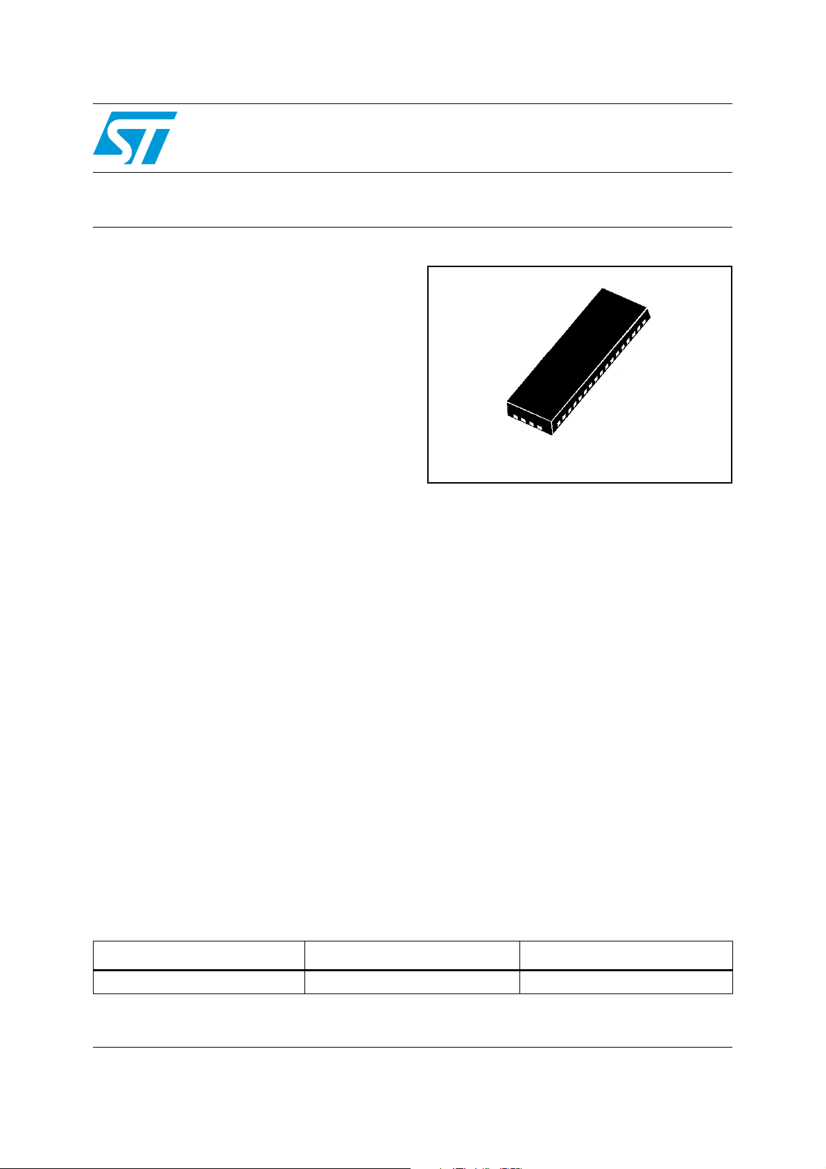
STMUX3040
TQFN42
Description
The STMUX3040 is a differential octal single pole
double throw (SPDT) bidirectional signal switch
with low R
standards such as PCIe gen 1, LVDS, TMDS and
video signaling.
The STMUX3040 features very low cross-talk,
low bit-to-bit skew, high channel-to-channel noise
isolation and low I/O capacitance.
The STMUX3040 switch offers very little or
practically no attenuation of the high speed
signals at the outputs, thus preserving the signal
integrity to pass stringent requirements.
. It is designed to support various
ON
Applications
■ Workstation
■ PC and notebooks
Table 1. Device summary
Order code Package Packaging
STMUX3040QTTR TQFN42 Tape and reel
October 2008 Rev 2 1/17
www.st.com
17
Page 2

Contents STMUX3040
Contents
1 Functional diagrams . . . . . . . . . . . . . . . . . . . . . . . . . . . . . . . . . . . . . . . . . 3
2 Pin settings . . . . . . . . . . . . . . . . . . . . . . . . . . . . . . . . . . . . . . . . . . . . . . . . 4
2.1 Pin connection . . . . . . . . . . . . . . . . . . . . . . . . . . . . . . . . . . . . . . . . . . . . . . 4
2.2 Pin description . . . . . . . . . . . . . . . . . . . . . . . . . . . . . . . . . . . . . . . . . . . . . . 5
2.3 Device operation table . . . . . . . . . . . . . . . . . . . . . . . . . . . . . . . . . . . . . . . . 6
3 Internal voltage regulator . . . . . . . . . . . . . . . . . . . . . . . . . . . . . . . . . . . . . 7
4 Maximum rating . . . . . . . . . . . . . . . . . . . . . . . . . . . . . . . . . . . . . . . . . . . . . 8
4.1 Absolute maximum rating . . . . . . . . . . . . . . . . . . . . . . . . . . . . . . . . . . . . . . 8
4.2 Thermal data . . . . . . . . . . . . . . . . . . . . . . . . . . . . . . . . . . . . . . . . . . . . . . . 8
5 Electrical specification . . . . . . . . . . . . . . . . . . . . . . . . . . . . . . . . . . . . . . . 9
5.1 DC electrical characteristics . . . . . . . . . . . . . . . . . . . . . . . . . . . . . . . . . . . . 9
5.2 Capacitance . . . . . . . . . . . . . . . . . . . . . . . . . . . . . . . . . . . . . . . . . . . . . . . 10
5.3 Power supply characteristics . . . . . . . . . . . . . . . . . . . . . . . . . . . . . . . . . . 10
5.4 Dynamic electrical characteristics . . . . . . . . . . . . . . . . . . . . . . . . . . . . . . 10
5.5 Dynamic switching characteristics . . . . . . . . . . . . . . . . . . . . . . . . . . . . . . 11
5.6 ESD performance . . . . . . . . . . . . . . . . . . . . . . . . . . . . . . . . . . . . . . . . . . . 11
6 Package mechanical data . . . . . . . . . . . . . . . . . . . . . . . . . . . . . . . . . . . . 12
7 Revision history . . . . . . . . . . . . . . . . . . . . . . . . . . . . . . . . . . . . . . . . . . . 16
2/17
Page 3
STMUX3040 Functional diagrams
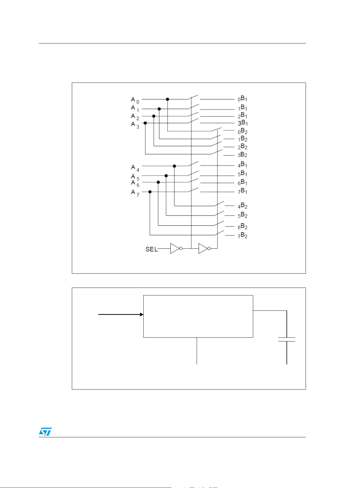
1 Functional diagrams
Figure 1. Functional diagram (switches)
Figure 2. Functional diagram (internal regulator)
3.3V to 1.8V Voltage Regulator
V33 (2.7V-3.3V)
(Bypassed when V33 < 2.2V)
GND GND
3/17
Vreg and VCC
Page 4
Pin settings STMUX3040
2 Pin settings
2.1 Pin connection
Figure 3. Pin connection (top through view)
Vcc GND Vcc GND
42 41 40 39
A0
A1
GND
Vcc
A2
A3
V33
SEL
GND
A4
A5
Vcc
GND
A6
A7
GND
10
11
12
13
14
15
16
17
1
2
3
4
5
6
7
8
9
18
19 20 21
38
37
34
33
32
31
30
29
28
27
26
25
24
23
22
0B1 GND
1B1
2B1
3B1
0B2
1B2
2B2
3B2
Vreg
4B1
5B1
6B1
7B1
4B2
5B2
6B2
7B2
Vcc GND Vcc GND
4/17
TQFN42
Page 5
STMUX3040 Pin settings
2.2 Pin description
Table 2. Pin description
Pin number Pin name Function
1 GND Ground
2A
3A
0
1
4 GND Ground
5Vcc
6A
7A
2
3
8V33
9 SEL Switch select pin
10 GND Ground
Switch
Switch
1.65 - 2.0 V supply
Tied to V
if V33 > 2.2 V
REG
Switch
Switch
2.7 V – 3.3 V (internal regulator active)
1.65 – 2.0 V (internal regulator bypassed)
11 A
12 A
13 Vcc
4
5
Switch
Switch
1.65 – 2.0 V supply
Tied to V
14 GND Ground
15 A
16 A
6
7
Switch
Switch
17 GND Ground
18 Vcc
1.65 – 2.0 V supply
Tied to V
19 GND Ground
20 Vcc
1.65 – 2.0 V supply
Tied to V
21 GND Ground
22
23
24
25
26
27
28
7B2
6B2
5B2
4B2
7B1
6B1
5B1
Switch
Switch
Switch
Switch
Switch
Switch
Switch
if V33>2.2V
REG
if V33>2.2V
REG
if V33>2.2V
REG
5/17
Page 6
Pin settings STMUX3040
Table 2. Pin description (continued)
Pin number Pin name Function
29
4B1
30 VREG
31
32
33
34
35
36
37
38
3B2
2B2
1B2
0B2
3B1
2B1
1B1
0B1
Switch
Output of internal regulator 22 nF capacitor required
here
Switch
Switch
Switch
Switch
Switch
Switch
Switch
Switch
39 GND Ground
40 Vcc
1.65 – 2.0 V supply
Tied to V
41 GND Ground
42 Vcc
1.65 – 2.0 V supply
Tied to V
if V33>2.2V
REG
if V33>2.2V
REG
2.3 Device operation table
Table 3. Operation table
SEL Function
LA
HA
to NB
N
to NB
N
1
2
6/17
Page 7

STMUX3040 Internal voltage regulator
3 Internal voltage regulator
The STMUX3040 is integrated with an internal voltage regulator. The voltage regulator is
activated when the supply voltage to the Vreg pin is more than 2.7 V. If the supply to V
less than 2.2 V, the regulator is bypassed.
Figure 4. Internal voltage regulator
Vcc GND Vcc GND
Vcc GND Vcc GND
42 41 40 39
42 41 40 39
reg
is
2.7V-
2.7V-
3.3V
3.3V
A0
A0
A1
A1
GND
GND
Vcc
Vcc
A2
A2
A3
A3
V33
V33
SEL
SEL
GND
GND
A4
A4
A5
A5
Vcc
Vcc
GND
GND
A6
A6
A7
A7
GND
GND
1
1
2
2
3
3
4
4
5
5
6
6
7
7
8
8
9
9
10
10
11
11
12
12
13
13
14
14
15
15
16
16
17
17
18
18
19 20 21
19 20 21
38
38
0B1GND
0B1GND
37
37
1B1
1B1
36
36
2B1
2B1
35
35
3B1
3B1
34
34
0B2
0B2
33
33
1B2
1B2
32
32
2B2
2B2
31
31
3B2
3B2
Vreg
Vreg
30
30
4B1
4B1
29
29
5B1
5B1
28
28
6B1
6B1
27
27
7B1
7B1
26
26
4B2
4B2
25
25
5B2
5B2
24
24
6B2
6B2
23
23
7B2
7B2
22
22
22nF
22nF
GND
GND
Vcc GND Vcc GND
Vcc GND Vcc GND
When the internal regulator is activated:
● V33 is used as supply input
● V
is used as output of the internal regulator, a 22 nF capacitor should be connected
reg
from this pin to ground
When internal regulator is not used:
● V
, V33 and V
CC
are all connected to 1.8 V supply
reg
7/17
Page 8

Maximum rating STMUX3040
4 Maximum rating
Stressing the device above the rating listed in the “Absolute Maximum Ratings” table may
cause permanent damage to the device. These are stress ratings only and operation of the
device at these or any other conditions above those indicated in the Operating sections of
this specification is not implied. Exposure to Absolute Maximum Rating conditions for
extended periods may affect device reliability. Refer also to the STMicroelectronics SURE
Program and other relevant quality documents.
4.1 Absolute maximum rating
Table 4. Absolute maximum rating
Symbol Parameter Value Unit
V
CC
V
33
V
I
V
IC
I
O
T
STG
T
L
1. VCC = 1.8 V ± 10% in regulator mode.
Supply voltage to ground -0.5 to +2.5 V
Supply voltage to internal regulator -0.5 to +4.5 V
DC input voltage -0.5 to Vcc
DC control input voltage -0.5 to Vcc
DC output current 120 mA
Storage temperature -65 to +150 °C
Lead temperature (10 sec) 300 °C
4.2 Thermal data
Table 5. Thermal data
Symbol Parameter Value Unit
R
thJA
Thermal resistance junction-ambient 40.8 °C/W
(1)
(1)
V
V
8/17
Page 9

STMUX3040 Electrical specification
5 Electrical specification
5.1 DC electrical characteristics
TA = -40 to +85°C, VCC = 1.8 V ± 10%
Table 6. SEL pin
Symbol Parameter Test conditions Min Typ Max Unit
V
V
V
High level input voltage High level guaranteed
IH
Low level input voltage Low level guaranteed -0.5
IL
= 1.8 V,
V
Clamp diode voltage
IK
I
Input high current
IH
I
Input low current
IL
CC
I
= -18 mA
IN
V
CC
V
= V
IN
V
CC
= GND
V
IN
= 1.8 V
CC
= 1.8 V,
0.65
Vcc
0.35
Vcc
-0.8 -1.2 V
±5 µA
±5 µA
Table 7. All signal switch pins
Symbol Parameter Test conditions Min Typ Max Unit
= 1.8 V
V
CC
= V
V
IN
CC
All non-tested switches
floating
= 1.8 V,
V
CC
I
= -18 mA
IN
V
= 1.8 V
CC
V
= 0.9 to V
IN
I
= -30 mA
IN
V
CC
= 0.9 to V
V
IN
I
= -30 mA
IN
V
CC
= 0.9 to V
V
IN
I
= -30 mA
IN
= 1.8 V
= 1.8 V
CC
CC
CC
1uA
-0.8 -1.2 V
5.5 8.0 Ω
11.3Ω
0.5 1 Ω
R
R
ΔR
I
IN
V
IK
ON
FLAT
ON
Input leakage
Clamp diode voltage
Switch ON resistance
ON resistance flatness
(1) (2)
ON resistance match
between channels
ΔR
(2) (3)
ON
= R
ONMAX
- R
ONMIN
(1)
V
V
1. Measured by voltage drop between channels at the indicated current through the switch.
2. Flatness is defined as the difference between the R
specified range on the same channel.
3. ΔRON measured at the same VCC, temperature and voltage level.
ONMAX
and the R
of the ON resistance over the
ONMIN
9/17
Page 10

Electrical specification STMUX3040
5.2 Capacitance
Table 8. Capacitance (TA = 25°C, f = 1 MHz)
Symbol Parameter Test conditions Min Typ Max Unit
C
C
Port x0 to port x1, switch off V
OFF
Capacitance switch on V
ON
= 0 V 4 pF
IN
= 0 V 6 pF
IN
5.3 Power supply characteristics
(
Table 9. Power supply characteristics (TA = -40 to +85 °C)
Symbol Parameter Test conditions Min Typ Max Unit
V
V33
Supply voltage (internal
CC
regulator inactive)
Supply voltage (internal
regulator active)
Quiescent power supply
I
current (internal regulator
CC
inactive)
Quiescent power supply
I
current (internal regulator
CC
active)
= 2.0 V,
V
CC
= V
CC
or GND
V
IN
V33 = 3.3V,
= 1.8V or GND
V
IN
5.4 Dynamic electrical characteristics
1.65 1.8 2.0 V
2.7 3.3 3.6 V
150 500 µA
250 700 µA
Table 10. Dynamic electrical characteristics (TA = -40 to +85 °C, VCC = 1.8 V ± 10%)
Symbol Parameter Test conditions Min Typ Max Unit
= 100 Ω,
R
X
O
L
f = 300 MHz
Non-adjacent channel
TA LK
Cross-talk
R
= 100 Ω,
L
f = 600 MHz
= 100 Ω,
R
L
f = 1200 MHz
RL = 100 Ω,
f = 300 MHz
R
= 100 Ω,
IRR
Off isolation
L
f = 600 MHz
= 100 Ω,
R
L
f = 1200 MHz
Data rate per channel 3.0 Gbps
D
R
-30 dB
-20 dB
-20 dB
-35 dB
-28 dB
-20 dB
BW Bandwidth -3dB bandwidth 1200 1300 MHz
10/17
Page 11

STMUX3040 Electrical specification
5.5 Dynamic switching characteristics
Table 11. Dynamic switching characteristics (TA = -40 to +85 °C, VCC = 1.8 V ± 10%)
Symbol Parameter Test conditions Min Typ Max Unit
Propagation delay VCC = 1.65 V - 2.0 V 0.25 ns
t
PD
t
t
t
t
t
SK(O)
t
SK(P)
t
Line enable time, SEL to x
PZH,
to x0 or x to x1
PZL
Line disable time, SEL to x
PHZ,
to x0 or x to x1
PLZ
= 1.65 V - 2.0V 0.5 6.5 9 ns
V
CC
= 1.65 V - 2.0 V 0.5 6.5 8.5 ns
V
CC
Output skew between
center port to any other
VCC = 1.65 V - 2.0 V 50 100 ps
port
Skew between opposite
transition of the same
output (t
t
Switching delay VCC = 1.65 V - 2.0 V 50 ns
ON
Switching delay VCC = 1.65 V - 2.0 V 30 ns
OFF
PHL
- t
PLH)
VCC = 1.65 V - 2.0 V 50 100 ps
5.6 ESD performance
Table 12. ESD performance
Symbol Parameter Test conditions Min Typ Max Unit
ESD IEC-61000-4-2
Air discharge
(10 pulses)
Contact discharge
(10 pulses)
±2kV
±2kV
11/17
Page 12

Package mechanical data STMUX3040
6 Package mechanical data
In order to meet environmental requirements, ST offers these devices in ECOPACK®
packages. These packages have a Lead-free second level interconnect . The category of
second level interconnect is marked on the package and on the inner box label, in
compliance with JEDEC Standard JESD97. The maximum ratings related to soldering
conditions are also marked on the inner box label. ECOPACK is an ST trademark.
ECOPACK specifications are available at: www.st.com.
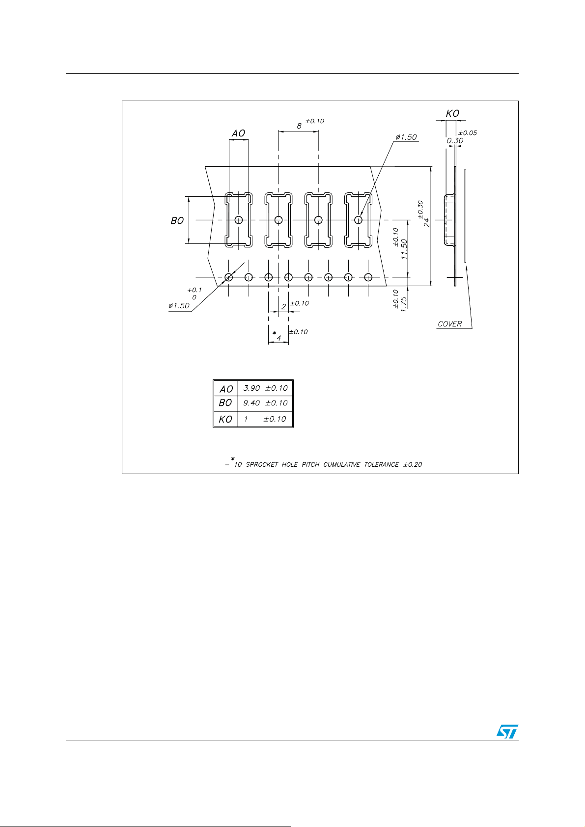
Figure 5. Package dimensions
12/17
Page 13

STMUX3040 Package mechanical data
Table 13. TQFN42 mechanical data
Millimeters
Symbol
Min Typ Max
A 0.70 0.75 0.80
A1 0 0.02 0.05
A3 0.20
b 0.20 0.25 0.30
D 3.40 3.50 3.60
D2 2 2.05 2.10
E 8.90 9 9.10
E2 7.50 7.55 7.60
e0.50
L 0.30 0.40 0.50
Figure 6. TQFN42 footprint recommendations
13/17
Page 14
Package mechanical data STMUX3040
Figure 7. Tape information
14/17
Page 15

STMUX3040 Package mechanical data
Figure 8. Reel information
15/17
Page 16
Revision history STMUX3040
7 Revision history
Table 14. Document revision history
Date Revision Changes
05-Jul-2007 1 Initial release.
Content reworked to improve readability, no technical content
change.
09-Oct-2008 2
Modified: title and datasheet cover page.
Added: Figure 7: Tape information on page 14, Figure 6: TQFN42
footprint recommendations on page 13 and Figure 8: Reel
information on page 15.
16/17
Page 17

STMUX3040
Please Read Carefully:
Information in this document is provided solely in connection with ST products. STMicroelectronics NV and its subsidiaries (“ST”) reserve the
right to make changes, corrections, modifications or improvements, to this document, and the products and services described herein at any
time, without notice.
All ST products are sold pursuant to ST’s terms and conditions of sale.
Purchasers are solely responsible for the choice, selection and use of the ST products and services described herein, and ST assumes no
liability whatsoever relating to the choice, selection or use of the ST products and services described herein.
No license, express or implied, by estoppel or otherwise, to any intellectual property rights is granted under this document. If any part of this
document refers to any third party products or services it shall not be deemed a license grant by ST for the use of such third party products
or services, or any intellectual property contained therein or considered as a warranty covering the use in any manner whatsoever of such
third party products or services or any intellectual property contained therein.
UNLESS OTHERWISE SET FORTH IN ST’S TERMS AND CONDITIONS OF SALE ST DISCLAIMS ANY EXPRESS OR IMPLIED
WARRANTY WITH RESPECT TO THE USE AND/OR SALE OF ST PRODUCTS INCLUDING WITHOUT LIMITATION IMPLIED
WARRANTIES OF MERCHANTABILITY, FITNESS FOR A PARTICULAR PURPOSE (AND THEIR EQUIVALENTS UNDER THE LAWS
OF ANY JURISDICTION), OR INFRINGEMENT OF ANY PATENT, COPYRIGHT OR OTHER INTELLECTUAL PROPERTY RIGHT.
UNLESS EXPRESSLY APPROVED IN WRITING BY AN AUTHORIZED ST REPRESENTATIVE, ST PRODUCTS ARE NOT
RECOMMENDED, AUTHORIZED OR WARRANTED FOR USE IN MILITARY, AIR CRAFT, SPACE, LIFE SAVING, OR LIFE SUSTAINING
APPLICATIONS, NOR IN PRODUCTS OR SYSTEMS WHERE FAILURE OR MALFUNCTION MAY RESULT IN PERSONAL INJURY,
DEATH, OR SEVERE PROPERTY OR ENVIRONMENTAL DAMAGE. ST PRODUCTS WHICH ARE NOT SPECIFIED AS "AUTOMOTIVE
GRADE" MAY ONLY BE USED IN AUTOMOTIVE APPLICATIONS AT USER’S OWN RISK.
Resale of ST products with provisions different from the statements and/or technical features set forth in this document shall immediately void
any warranty granted by ST for the ST product or service described herein and shall not create or extend in any manner whatsoever, any
liability of ST.
ST and the ST logo are trademarks or registered trademarks of ST in various countries.
Information in this document supersedes and replaces all information previously supplied.
The ST logo is a registered trademark of STMicroelectronics. All other names are the property of their respective owners.
© 2008 STMicroelectronics - All rights reserved
STMicroelectronics group of companies
Australia - Belgium - Brazil - Canada - China - Czech Republic - Finland - France - Germany - Hong Kong - India - Israel - Italy - Japan -
Malaysia - Malta - Morocco - Singapore - Spain - Sweden - Switzerland - United Kingdom - United States of America
www.st.com
17/17
 Loading...