How it Works
Log In / Sign Up
Buy Points
How it Works
FAQ
Contact Us
Questions and Suggestions
Users
ST
Loading...
S
STM32G071B-DISCO
STM32G4A1xE
STM32G4 Nucleo-64
STM32H745I-DISCO
STM32H747I-DISCO
STM32H747I-EVAL
STM32H747XI MCU
STM32H74xI/G
STM32H750B-DK
STM32H757I-EVAL
STM32H75xI/G
STM32L
STM32L0538-DISCO
STM32L073Z-EVAL
STM32L0 Series
STM32L151C6
STM32L151C8
STM32L151CB
STM32L151QC
STM32L151QD
STM32L151R6
STM32L151R8
STM32L151RB
STM32L151RC
STM32L151RD
STM32L151V8
STM32L151VB
STM32L151VC
STM32L151VD
STM32L151ZC
STM32L151ZD
STM32L152
STM32L152C6
STM32L152C8
STM32L152CB
STM32L152D
STM32L152-EVAL
STM32L152QC
STM32L152QD
STM32L152R6
STM32L152R8
STM32L152RB
STM32L152RC
STM32L152RD
STM32L152V8
STM32L152VB
2
STM32L152VBT6
STM32L152VC
STM32L152VD
STM32L152ZC
STM32L152ZD
STM32L162QD
STM32L162RD
STM32L162VD
STM32L162ZD
STM32L1 Series
2
STM32L4
STM32L4R9I-EVAL
STM32L4 Series
3
STM32L4x6
STM32MP157A-DK1
STM32MP157A-EV1
STM32MP157C-DK2
STM32MP157C-EV1
STM32MP157 Series
STM32TS60
STM32VL
STM32W108C8
2
STM32W108CB
2
STM32W108CC
STM32W108CZ
STM32W108HB
2
STM32W-EXT
STM32W-SK
STM351-2
STM6315
STm6316
STM6321
STM6322
STM6502
STM6503
STM6504
STM6505
STM6510
STM6513
STM6519
STM6520
STM6522
STM6524
STM6600
STM6601
STM6700
STM6710
STM6717
STM6718
STM6719
STM6720
STM6777
STM6778
STM6779
Loading...
Loading...
Nothing found
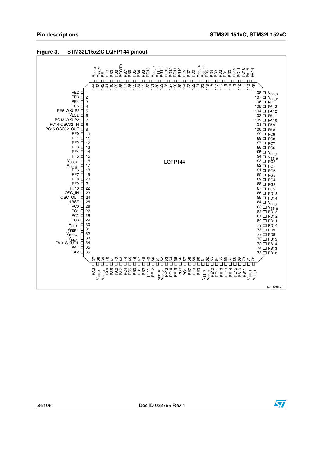
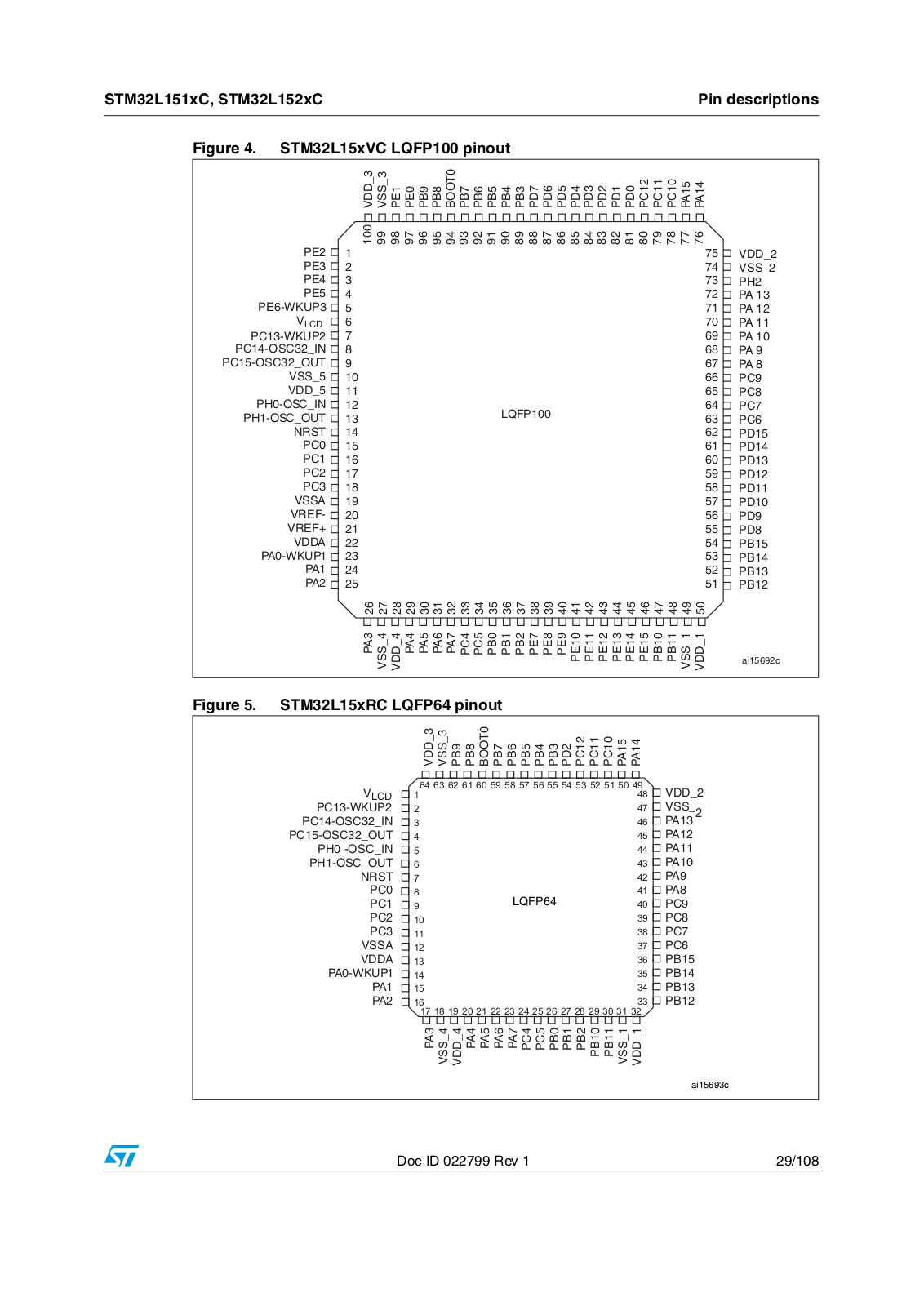
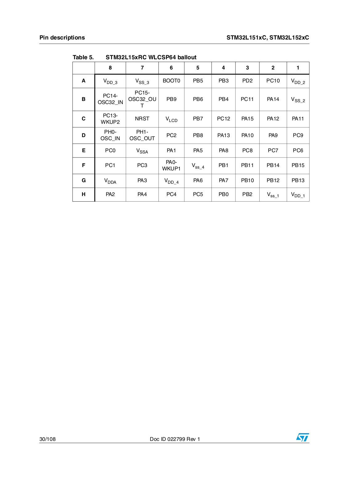
STM32L152ZC
User Manual
108 pgs
2.18 Mb
0
Table of contents
Loading...
ST STM32L151QC, STM32L151RC, STM32L151VC, STM32L151ZC, STM32L152QC User Manual
...
ST STM32L151QC, STM32L151RC, STM32L151VC, STM32L151ZC, STM32L152QC, STM32L152RC, STM32L152VC, STM32L152ZC User Manual
Download
Specifications and Main Features
Frequently Asked Questions
User Manual
Download
Loading...
+
78
hidden pages
Unhide
You need points to download manuals.
1 point = 1 manual.
You can buy points or you can get point for every manual you upload.
Buy points
Upload your manuals