

Page 1
STM32G4A1xE
LQFP48 (7 x 7 mm)
LQFP64 (10 x 10 mm)
LQFP80 (12 x 12 mm)
UFBGA64
(5 x 5 mm)
UFQFPN32 (5 x 5 mm)
UFQFPN48 (7 x 7 mm)
WLCSP64
(Pitch 0.4)
FBGA
LQFP80 (14 x 14 mm)
LQFP100 (14 x 14 mm)
Arm® Cortex®-M4 32-bit MCU+FPU, 170 MHz / 213 DMIPS, up to
512 KB Flash, 112 KB SRAM, rich analog, math accelerator, AES
Datasheet - production data
Features
• Core: Arm® 32-bit Cortex®-M4 CPU with FPU,
Adaptive real-time accelerator (ART
Accelerator) allowing 0-wait-state execution
from Flash memory, frequency up to 170 MHz
with 213 DMIPS, MPU, DSP instructions
• Operating conditions:
–V
• Mathematical hardware accelerators
– CORDIC for trigonometric functions
– FMAC: filter mathematical accelerator
• Memories
– 512 Kbytes of Flash memory with ECC
– 96 Kbytes of SRAM, with hardware parity
– Routine booster: 16 Kbytes of SRAM on
– Quad-SPI memory interface
• Reset and supply management
– Power-on/power-down reset
– Programmable voltage detector (PVD)
– Low-power modes: sleep, stop, standby
–V
• Clock management
–4
– 32 kHz oscillator with calibration
– Internal 16 MHz RC with PLL option (± 1%)
–
• Up to 86 fast I/Os
– All mappable on external interrupt vectors
, V
DD
voltage range:
DDA
1.71 V to 3.6 V
acceleration
support, proprietary code readout
protection (PCROP), securable memory
area, 1 Kbyte OTP
check implemented on the first 32 Kbytes
instruction and data bus, with hardware
parity check (CCM SRAM)
(POR/PDR/BOR)
and shutdown
supply for RTC and backup registers
BAT
to 48 MHz crystal oscillator
Internal 32 kHz RC oscillator (± 5%)
– Several I/Os with 5 V tolerant capability
• Interconnect matrix
• 16-channel DMA controller
• 3 x ADCs 0.25 µs (up to 36 channels).
Resolution up to 16-bit with hardware
oversampling, 0 to 3.6 V conversion range
• 4 x 12-bit DAC channels
– 2 x buffered external channels 1 MSPS
– 2 x unbuffered internal channels 15 MSPS
• 4 x ultra-fast rail-to-rail analog comparators
• 4 x operational amplifiers that can be used in
PGA mode, all terminals accessible
• Internal voltage reference buffer (VREFBUF)
supporting three output voltages (2.048 V,
2.5 V, 2.9 V)
• 15 timers:
– 1 x 32-bit timer and 2 x 16-bit timers with up
to four IC/OC/PWM or pulse counter and
quadrature (incremental) encoder input
– 3 x 16-bit 8-channel advanced motor
control timers, with up to 8 x PWM
channels, dead time generation and
emergency stop
– 1 x 16-bit timer with 2 x IC/OCs, one
OCN/PWM, dead time generation and
emergency stop
– 2 x 16-bit timers with IC/OC/OCN/PWM,
dead time generation and emergency stop
– 2 x watchdog timers (independent, window)
– 1 x SysTick timer: 24-bit downcounter
– 2 x 16-bit basic timers
November 2020 DS13268 Rev 2 1/200
This is information on a product in full production.
www.st.com
Page 2
STM32G4A1xE
– 1 x low-power timer
• Calendar RTC with alarm, periodic wakeup
from stop/standby
• Communication interfaces
– 2 x FDCAN controller supporting flexible
data rate
– 3 x I
2
C Fast mode plus (1 Mbit/s) with
20 mA current sink, SMBus/PMBus,
wakeup from stop
– 5 x USART/UARTs (ISO 7816 interface,
LIN, IrDA, modem control)
–1 x LPUART
– 3 x SPIs, 4 to 16 programmable bit frames,
2 x with multiplexed half duplex I
2
S
– 1 x SAI (serial audio interface)
– USB 2.0 full-speed interface with LPM and
BCD support
– IRTIM (infrared interface)
– USB Type-C™ /USB power delivery
controller (UCPD)
• True random number generator (RNG)
• CRC calculation unit, 96-bit unique ID
• AES: 128/256-bit key encryption hardware
accelerator
• Development support: serial wire debug
(SWD), JTAG, Embedded Trace Macrocell™
interface
Table 1. Device summary
Reference Part number
STM32G4A1xE STM32G4A1CE, STM32G4A1KE, STM32G4A1ME, STM32G4A1RE, STM32G4A1VE
2/200 DS13268 Rev 2
Page 3

STM32G4A1xE Contents
Contents
1 Introduction . . . . . . . . . . . . . . . . . . . . . . . . . . . . . . . . . . . . . . . . . . . . . . . 12
2 Description . . . . . . . . . . . . . . . . . . . . . . . . . . . . . . . . . . . . . . . . . . . . . . . . 13
3 Functional overview . . . . . . . . . . . . . . . . . . . . . . . . . . . . . . . . . . . . . . . . 17
3.1 Arm® Cortex®-M4 core with FPU . . . . . . . . . . . . . . . . . . . . . . . . . . . . . . . 17
3.2 Adaptive real-time memory accelerator (ART accelerator) . . . . . . . . . . . 17
3.3 Memory protection unit . . . . . . . . . . . . . . . . . . . . . . . . . . . . . . . . . . . . . . . 17
3.4 Embedded Flash memory . . . . . . . . . . . . . . . . . . . . . . . . . . . . . . . . . . . . 17
3.5 Embedded SRAM . . . . . . . . . . . . . . . . . . . . . . . . . . . . . . . . . . . . . . . . . . . 18
3.6 Multi-AHB bus matrix . . . . . . . . . . . . . . . . . . . . . . . . . . . . . . . . . . . . . . . . 19
3.7 Boot modes . . . . . . . . . . . . . . . . . . . . . . . . . . . . . . . . . . . . . . . . . . . . . . . 19
3.8 CORDIC . . . . . . . . . . . . . . . . . . . . . . . . . . . . . . . . . . . . . . . . . . . . . . . . . . 20
3.9 Filter mathematical accelerator (FMAC) . . . . . . . . . . . . . . . . . . . . . . . . . . 20
3.10 Cyclic redundancy check calculation unit (CRC) . . . . . . . . . . . . . . . . . . . 21
3.11 Power supply management . . . . . . . . . . . . . . . . . . . . . . . . . . . . . . . . . . . 21
3.11.1 Power supply schemes . . . . . . . . . . . . . . . . . . . . . . . . . . . . . . . . . . . . . 21
3.11.2 Power supply supervisor . . . . . . . . . . . . . . . . . . . . . . . . . . . . . . . . . . . . 22
3.11.3 Voltage regulator . . . . . . . . . . . . . . . . . . . . . . . . . . . . . . . . . . . . . . . . . . 22
3.11.4 Low-power modes . . . . . . . . . . . . . . . . . . . . . . . . . . . . . . . . . . . . . . . . . 23
3.11.5 Reset mode . . . . . . . . . . . . . . . . . . . . . . . . . . . . . . . . . . . . . . . . . . . . . . 23
3.11.6 VBAT operation . . . . . . . . . . . . . . . . . . . . . . . . . . . . . . . . . . . . . . . . . . . 23
3.12 Interconnect matrix . . . . . . . . . . . . . . . . . . . . . . . . . . . . . . . . . . . . . . . . . . 25
3.13 Clocks and startup . . . . . . . . . . . . . . . . . . . . . . . . . . . . . . . . . . . . . . . . . . 26
3.14 General-purpose inputs/outputs (GPIOs) . . . . . . . . . . . . . . . . . . . . . . . . . 27
3.15 Direct memory access controller (DMA) . . . . . . . . . . . . . . . . . . . . . . . . . . 27
3.16 DMA request router (DMAMux) . . . . . . . . . . . . . . . . . . . . . . . . . . . . . . . . 28
3.17 Interrupts and events . . . . . . . . . . . . . . . . . . . . . . . . . . . . . . . . . . . . . . . . 28
3.17.1 Nested vectored interrupt controller (NVIC) . . . . . . . . . . . . . . . . . . . . . . 28
3.17.2 Extended interrupt/event controller (EXTI) . . . . . . . . . . . . . . . . . . . . . . 28
3.18 Analog-to-digital converter (ADC) . . . . . . . . . . . . . . . . . . . . . . . . . . . . . . 29
3.18.1 Temperature sensor . . . . . . . . . . . . . . . . . . . . . . . . . . . . . . . . . . . . . . . . 29
DS13268 Rev 2 3/200
6
Page 4

Contents STM32G4A1xE
3.18.2 Internal voltage reference (VREFINT) . . . . . . . . . . . . . . . . . . . . . . . . . . 30
3.18.3 VBAT battery voltage monitoring . . . . . . . . . . . . . . . . . . . . . . . . . . . . . . 30
3.18.4 Operational amplifier internal output (OPAMPxINT): . . . . . . . . . . . . . . . 30
3.19 Digital to analog converter (DAC) . . . . . . . . . . . . . . . . . . . . . . . . . . . . . . . 30
3.20 Voltage reference buffer (VREFBUF) . . . . . . . . . . . . . . . . . . . . . . . . . . . . 31
3.21 Comparators (COMP) . . . . . . . . . . . . . . . . . . . . . . . . . . . . . . . . . . . . . . . 32
3.22 Operational amplifier (OPAMP) . . . . . . . . . . . . . . . . . . . . . . . . . . . . . . . . 32
3.23 Random number generator (RNG) . . . . . . . . . . . . . . . . . . . . . . . . . . . . . . 32
3.24 Advanced encryption standard hardware accelerator (AES) . . . . . . . . . . 32
3.25 Timers and watchdogs . . . . . . . . . . . . . . . . . . . . . . . . . . . . . . . . . . . . . . . 33
3.25.1 Advanced motor control timer (TIM1, TIM8, TIM20) . . . . . . . . . . . . . . . 34
3.25.2 General-purpose timers (TIM2, TIM3, TIM4, TIM15, TIM16,
TIM17) . . . . . . . . . . . . . . . . . . . . . . . . . . . . . . . . . . . . . . . . . . . . . . . . . . 35
3.25.3 Basic timers (TIM6 and TIM7) . . . . . . . . . . . . . . . . . . . . . . . . . . . . . . . . 35
3.25.4 Low-power timer (LPTIM1) . . . . . . . . . . . . . . . . . . . . . . . . . . . . . . . . . . 36
3.25.5 Independent watchdog (IWDG) . . . . . . . . . . . . . . . . . . . . . . . . . . . . . . . 36
3.25.6 System window watchdog (WWDG) . . . . . . . . . . . . . . . . . . . . . . . . . . . 36
3.25.7 SysTick timer . . . . . . . . . . . . . . . . . . . . . . . . . . . . . . . . . . . . . . . . . . . . . 36
3.26 Real-time clock (RTC) and backup registers . . . . . . . . . . . . . . . . . . . . . . 37
3.27 Tamper and backup registers (TAMP) . . . . . . . . . . . . . . . . . . . . . . . . . . . 37
3.28 Infrared transmitter . . . . . . . . . . . . . . . . . . . . . . . . . . . . . . . . . . . . . . . . . . 38
3.29 Inter-integrated circuit interface (I
2
C) . . . . . . . . . . . . . . . . . . . . . . . . . . . . 39
3.30 Universal synchronous/asynchronous receiver transmitter (USART) . . . 40
3.31 Low-power universal asynchronous receiver transmitter (LPUART) . . . . 41
3.32 Serial peripheral interface (SPI) . . . . . . . . . . . . . . . . . . . . . . . . . . . . . . . . 41
3.33 Serial audio interfaces (SAI) . . . . . . . . . . . . . . . . . . . . . . . . . . . . . . . . . . . 42
3.33.1 SAI peripheral supports . . . . . . . . . . . . . . . . . . . . . . . . . . . . . . . . . . . . . 42
3.34 Controller area network (FDCAN1, FDCAN2) . . . . . . . . . . . . . . . . . . . . . 43
3.35 Universal serial bus (USB) . . . . . . . . . . . . . . . . . . . . . . . . . . . . . . . . . . . . 43
3.36 USB Type-C™ / USB Power Delivery controller (UCPD) . . . . . . . . . . . . . 43
3.37 Clock recovery system (CRS) . . . . . . . . . . . . . . . . . . . . . . . . . . . . . . . . . 44
3.38 Quad SPI memory interface (QUADSPI) . . . . . . . . . . . . . . . . . . . . . . . . . 44
3.39 Development support . . . . . . . . . . . . . . . . . . . . . . . . . . . . . . . . . . . . . . . . 45
3.39.1 Serial wire JTAG debug port (SWJ-DP) . . . . . . . . . . . . . . . . . . . . . . . . . 45
3.39.2 Embedded trace macrocell™ . . . . . . . . . . . . . . . . . . . . . . . . . . . . . . . . 45
4/200 DS13268 Rev 2
Page 5

STM32G4A1xE Contents
4 Pinouts and pin description . . . . . . . . . . . . . . . . . . . . . . . . . . . . . . . . . . 46
4.1 UFQFPN32 pinout description . . . . . . . . . . . . . . . . . . . . . . . . . . . . . . . . . 46
4.2 UFQFPN48 pinout description . . . . . . . . . . . . . . . . . . . . . . . . . . . . . . . . . 47
4.3 LQFP48 pinout description . . . . . . . . . . . . . . . . . . . . . . . . . . . . . . . . . . . . 47
4.4 WLCSP64 ballout description . . . . . . . . . . . . . . . . . . . . . . . . . . . . . . . . . . 48
4.5 LQFP64 pinout description . . . . . . . . . . . . . . . . . . . . . . . . . . . . . . . . . . . . 48
4.6 UFBGA64 ballout description . . . . . . . . . . . . . . . . . . . . . . . . . . . . . . . . . . 49
4.7 LQFP80 pinout description . . . . . . . . . . . . . . . . . . . . . . . . . . . . . . . . . . . . 50
4.8 LQFP100 pinout description . . . . . . . . . . . . . . . . . . . . . . . . . . . . . . . . . . . 51
4.9 Pin definition . . . . . . . . . . . . . . . . . . . . . . . . . . . . . . . . . . . . . . . . . . . . . . . 52
4.10 Alternate functions . . . . . . . . . . . . . . . . . . . . . . . . . . . . . . . . . . . . . . . . . . 64
5 Electrical characteristics . . . . . . . . . . . . . . . . . . . . . . . . . . . . . . . . . . . . 70
5.1 Parameter conditions . . . . . . . . . . . . . . . . . . . . . . . . . . . . . . . . . . . . . . . . 70
5.1.1 Minimum and maximum values . . . . . . . . . . . . . . . . . . . . . . . . . . . . . . . 70
5.1.2 Typical values . . . . . . . . . . . . . . . . . . . . . . . . . . . . . . . . . . . . . . . . . . . . 70
5.1.3 Typical curves . . . . . . . . . . . . . . . . . . . . . . . . . . . . . . . . . . . . . . . . . . . . 70
5.1.4 Loading capacitor . . . . . . . . . . . . . . . . . . . . . . . . . . . . . . . . . . . . . . . . . 70
5.1.5 Pin input voltage . . . . . . . . . . . . . . . . . . . . . . . . . . . . . . . . . . . . . . . . . . 70
5.1.6 Power supply scheme . . . . . . . . . . . . . . . . . . . . . . . . . . . . . . . . . . . . . . 71
5.1.7 Current consumption measurement . . . . . . . . . . . . . . . . . . . . . . . . . . . 72
5.2 Absolute maximum ratings . . . . . . . . . . . . . . . . . . . . . . . . . . . . . . . . . . . . 72
5.3 Operating conditions . . . . . . . . . . . . . . . . . . . . . . . . . . . . . . . . . . . . . . . . 74
5.3.1 General operating conditions . . . . . . . . . . . . . . . . . . . . . . . . . . . . . . . . . 74
5.3.2 Operating conditions at power-up / power-down . . . . . . . . . . . . . . . . . . 75
5.3.3 Embedded reset and power control block characteristics . . . . . . . . . . . 75
5.3.4 Embedded voltage reference . . . . . . . . . . . . . . . . . . . . . . . . . . . . . . . . . 77
5.3.5 Supply current characteristics . . . . . . . . . . . . . . . . . . . . . . . . . . . . . . . . 78
5.3.6 Wakeup time from low-power modes and voltage scaling
transition times . . . . . . . . . . . . . . . . . . . . . . . . . . . . . . . . . . . . . . . . . . . 100
5.3.7 External clock source characteristics . . . . . . . . . . . . . . . . . . . . . . . . . . 101
5.3.8 Internal clock source characteristics . . . . . . . . . . . . . . . . . . . . . . . . . . 106
5.3.9 PLL characteristics . . . . . . . . . . . . . . . . . . . . . . . . . . . . . . . . . . . . . . . . 109
5.3.10 Flash memory characteristics . . . . . . . . . . . . . . . . . . . . . . . . . . . . . . . 110
5.3.11 EMC characteristics . . . . . . . . . . . . . . . . . . . . . . . . . . . . . . . . . . . . . . . 111
5.3.12 Electrical sensitivity characteristics . . . . . . . . . . . . . . . . . . . . . . . . . . . 112
DS13268 Rev 2 5/200
6
Page 6

Contents STM32G4A1xE
5.3.13 I/O current injection characteristics . . . . . . . . . . . . . . . . . . . . . . . . . . . 113
5.3.14 I/O port characteristics . . . . . . . . . . . . . . . . . . . . . . . . . . . . . . . . . . . . . 114
5.3.15 NRST pin characteristics . . . . . . . . . . . . . . . . . . . . . . . . . . . . . . . . . . . 119
5.3.16 Extended interrupt and event controller input (EXTI) characteristics . . 120
5.3.17 Analog switches booster . . . . . . . . . . . . . . . . . . . . . . . . . . . . . . . . . . . 120
5.3.18 Analog-to-digital converter characteristics . . . . . . . . . . . . . . . . . . . . . . 121
5.3.19 Digital-to-Analog converter characteristics . . . . . . . . . . . . . . . . . . . . . 136
5.3.20 Voltage reference buffer characteristics . . . . . . . . . . . . . . . . . . . . . . . 143
5.3.21 Comparator characteristics . . . . . . . . . . . . . . . . . . . . . . . . . . . . . . . . . 146
5.3.22 Operational amplifiers characteristics . . . . . . . . . . . . . . . . . . . . . . . . . 147
5.3.23 Temperature sensor characteristics . . . . . . . . . . . . . . . . . . . . . . . . . . . 151
5.3.24 V
5.3.25 Timer characteristics . . . . . . . . . . . . . . . . . . . . . . . . . . . . . . . . . . . . . . 152
5.3.26 Communication interfaces characteristics . . . . . . . . . . . . . . . . . . . . . . 153
5.3.27 QUADSPI characteristics . . . . . . . . . . . . . . . . . . . . . . . . . . . . . . . . . . . 163
5.3.28 UCPD characteristics . . . . . . . . . . . . . . . . . . . . . . . . . . . . . . . . . . . . . . 165
monitoring characteristics . . . . . . . . . . . . . . . . . . . . . . . . . . . . . . 151
BAT
6 Package information . . . . . . . . . . . . . . . . . . . . . . . . . . . . . . . . . . . . . . . 166
6.1 UFQFPN32 package information . . . . . . . . . . . . . . . . . . . . . . . . . . . . . . 166
6.2 UFQFPN48 package information . . . . . . . . . . . . . . . . . . . . . . . . . . . . . . 169
6.3 LQFP48 package information . . . . . . . . . . . . . . . . . . . . . . . . . . . . . . . . . 172
6.4 WLCSP64 package information . . . . . . . . . . . . . . . . . . . . . . . . . . . . . . . 176
6.5 LQFP64 package information . . . . . . . . . . . . . . . . . . . . . . . . . . . . . . . . . 179
6.6 UFBGA64 package information . . . . . . . . . . . . . . . . . . . . . . . . . . . . . . . 182
6.7 LQFP80 12 x 12 mm package information . . . . . . . . . . . . . . . . . . . . . . . 185
6.8 LQFP80 14 x 14 mm package information . . . . . . . . . . . . . . . . . . . . . . . 188
6.9 LQFP100 package information . . . . . . . . . . . . . . . . . . . . . . . . . . . . . . . . 191
6.10 Thermal characteristics . . . . . . . . . . . . . . . . . . . . . . . . . . . . . . . . . . . . . 194
6.10.1 Reference document . . . . . . . . . . . . . . . . . . . . . . . . . . . . . . . . . . . . . . 195
6.10.2 Selecting the product temperature range . . . . . . . . . . . . . . . . . . . . . . 196
7 Ordering information . . . . . . . . . . . . . . . . . . . . . . . . . . . . . . . . . . . . . . 198
8 Revision history . . . . . . . . . . . . . . . . . . . . . . . . . . . . . . . . . . . . . . . . . . 199
6/200 DS13268 Rev 2
Page 7

STM32G4A1xE List of tables
List of tables
Table 1. Device summary . . . . . . . . . . . . . . . . . . . . . . . . . . . . . . . . . . . . . . . . . . . . . . . . . . . . . . . . . . 2
Table 2. STM32G4A1xE features and peripheral counts . . . . . . . . . . . . . . . . . . . . . . . . . . . . . . . . . 14
Table 3. STM32G4A1xE peripherals interconnect matrix. . . . . . . . . . . . . . . . . . . . . . . . . . . . . . . . . 25
Table 4. DMA implementation . . . . . . . . . . . . . . . . . . . . . . . . . . . . . . . . . . . . . . . . . . . . . . . . . . . . . 27
Table 5. Temperature sensor calibration values. . . . . . . . . . . . . . . . . . . . . . . . . . . . . . . . . . . . . . . . 30
Table 6. Internal voltage reference calibration values . . . . . . . . . . . . . . . . . . . . . . . . . . . . . . . . . . . 30
Table 7. Timer feature comparison . . . . . . . . . . . . . . . . . . . . . . . . . . . . . . . . . . . . . . . . . . . . . . . . . . 33
Table 8. I2C implementation . . . . . . . . . . . . . . . . . . . . . . . . . . . . . . . . . . . . . . . . . . . . . . . . . . . . . . . 39
Table 9. USART/UART/LPUART features . . . . . . . . . . . . . . . . . . . . . . . . . . . . . . . . . . . . . . . . . . . . 40
Table 10. SAI implementation for the features implementation . . . . . . . . . . . . . . . . . . . . . . . . . . . . . 42
Table 11. Legend/abbreviations used in the pinout table . . . . . . . . . . . . . . . . . . . . . . . . . . . . . . . . . . 52
Table 12. STM32G4A1xE pin definition . . . . . . . . . . . . . . . . . . . . . . . . . . . . . . . . . . . . . . . . . . . . . . . 53
Table 13. Alternate function . . . . . . . . . . . . . . . . . . . . . . . . . . . . . . . . . . . . . . . . . . . . . . . . . . . . . . . . 64
Table 14. Voltage characteristics . . . . . . . . . . . . . . . . . . . . . . . . . . . . . . . . . . . . . . . . . . . . . . . . . . . . 72
Table 15. Current characteristics . . . . . . . . . . . . . . . . . . . . . . . . . . . . . . . . . . . . . . . . . . . . . . . . . . . . 73
Table 16. Thermal characteristics. . . . . . . . . . . . . . . . . . . . . . . . . . . . . . . . . . . . . . . . . . . . . . . . . . . . 73
Table 17. General operating conditions . . . . . . . . . . . . . . . . . . . . . . . . . . . . . . . . . . . . . . . . . . . . . . . 74
Table 18. Operating conditions at power-up / power-down . . . . . . . . . . . . . . . . . . . . . . . . . . . . . . . . 75
Table 19. Embedded reset and power control block characteristics. . . . . . . . . . . . . . . . . . . . . . . . . . 75
Table 20. Embedded internal voltage reference. . . . . . . . . . . . . . . . . . . . . . . . . . . . . . . . . . . . . . . . . 77
Table 21. Current consumption in Run and Low-power run modes, code with data
processing running from Flash in single Bank, ART enable (Cache ON Prefetch OFF) . . 79
Table 22. Current consumption in Run and Low-power run modes,
code with data processing running from SRAM1 . . . . . . . . . . . . . . . . . . . . . . . . . . . . . . . . 81
Table 23. Typical current consumption in Run and Low-power run modes, with different codes
running from Flash, ART enable (Cache ON Prefetch OFF) . . . . . . . . . . . . . . . . . . . . . . . 83
Table 24. Typical current consumption in Run and Low-power run modes, with different codes
running from SRAM1 . . . . . . . . . . . . . . . . . . . . . . . . . . . . . . . . . . . . . . . . . . . . . . . . . . . . . 84
Table 25. Typical current consumption in Run and Low-power run modes, with different codes
running from SRAM2 . . . . . . . . . . . . . . . . . . . . . . . . . . . . . . . . . . . . . . . . . . . . . . . . . . . . . 85
Table 26. Typical current consumption in Run and Low-power run modes, with different codes
running from CCM . . . . . . . . . . . . . . . . . . . . . . . . . . . . . . . . . . . . . . . . . . . . . . . . . . . . . . . 86
Table 27. Current consumption in Sleep and Low-power sleep mode Flash ON . . . . . . . . . . . . . . . . 87
Table 28. Current consumption in low-power sleep modes, Flash in power-down . . . . . . . . . . . . . . . 88
Table 29. Current consumption in Stop 1 mode . . . . . . . . . . . . . . . . . . . . . . . . . . . . . . . . . . . . . . . . . 89
Table 30. Current consumption in Stop 0 mode . . . . . . . . . . . . . . . . . . . . . . . . . . . . . . . . . . . . . . . . . 90
Table 31. Current consumption in Standby mode . . . . . . . . . . . . . . . . . . . . . . . . . . . . . . . . . . . . . . . 90
Table 32. Current consumption in Shutdown mode . . . . . . . . . . . . . . . . . . . . . . . . . . . . . . . . . . . . . . 92
Table 33. Current consumption in VBAT mode . . . . . . . . . . . . . . . . . . . . . . . . . . . . . . . . . . . . . . . . . 94
Table 34. Peripheral current consumption . . . . . . . . . . . . . . . . . . . . . . . . . . . . . . . . . . . . . . . . . . . . . 96
Table 35. Low-power mode wakeup timings . . . . . . . . . . . . . . . . . . . . . . . . . . . . . . . . . . . . . . . . . . 100
Table 36. Regulator modes transition times . . . . . . . . . . . . . . . . . . . . . . . . . . . . . . . . . . . . . . . . . . . 101
Table 37. Wakeup time using USART/LPUART. . . . . . . . . . . . . . . . . . . . . . . . . . . . . . . . . . . . . . . . 101
Table 38. High-speed external user clock characteristics. . . . . . . . . . . . . . . . . . . . . . . . . . . . . . . . . 101
Table 39. Low-speed external user clock characteristics . . . . . . . . . . . . . . . . . . . . . . . . . . . . . . . . . 102
Table 40. HSE oscillator characteristics . . . . . . . . . . . . . . . . . . . . . . . . . . . . . . . . . . . . . . . . . . . . . . 103
Table 41. LSE oscillator characteristics (f
Table 42. HSI16 oscillator characteristics. . . . . . . . . . . . . . . . . . . . . . . . . . . . . . . . . . . . . . . . . . . . . 106
= 32.768 kHz) . . . . . . . . . . . . . . . . . . . . . . . . . . . . . . 105
LSE
DS13268 Rev 2 7/200
9
Page 8

List of tables STM32G4A1xE
Table 43. HSI48 oscillator characteristics. . . . . . . . . . . . . . . . . . . . . . . . . . . . . . . . . . . . . . . . . . . . . 107
Table 44. LSI oscillator characteristics . . . . . . . . . . . . . . . . . . . . . . . . . . . . . . . . . . . . . . . . . . . . . . . 108
Table 45. PLL characteristics . . . . . . . . . . . . . . . . . . . . . . . . . . . . . . . . . . . . . . . . . . . . . . . . . . . . . . 109
Table 46. Flash memory characteristics . . . . . . . . . . . . . . . . . . . . . . . . . . . . . . . . . . . . . . . . . . . . . . 110
Table 47. Flash memory endurance and data retention. . . . . . . . . . . . . . . . . . . . . . . . . . . . . . . . . . 110
Table 48. EMS characteristics . . . . . . . . . . . . . . . . . . . . . . . . . . . . . . . . . . . . . . . . . . . . . . . . . . . . . 111
Table 49. EMI characteristics . . . . . . . . . . . . . . . . . . . . . . . . . . . . . . . . . . . . . . . . . . . . . . . . . . . . . . 112
Table 50. ESD absolute maximum ratings . . . . . . . . . . . . . . . . . . . . . . . . . . . . . . . . . . . . . . . . . . . . 112
Table 51. Electrical sensitivities . . . . . . . . . . . . . . . . . . . . . . . . . . . . . . . . . . . . . . . . . . . . . . . . . . . . 113
Table 52. I/O current injection susceptibility . . . . . . . . . . . . . . . . . . . . . . . . . . . . . . . . . . . . . . . . . . . 113
Table 53. I/O static characteristics . . . . . . . . . . . . . . . . . . . . . . . . . . . . . . . . . . . . . . . . . . . . . . . . . . 114
Table 54. Output voltage characteristics . . . . . . . . . . . . . . . . . . . . . . . . . . . . . . . . . . . . . . . . . . . . . 116
Table 55. I/O (except FT_c) AC characteristics . . . . . . . . . . . . . . . . . . . . . . . . . . . . . . . . . . . . . . . . 117
Table 56. I/O FT_c AC characteristics . . . . . . . . . . . . . . . . . . . . . . . . . . . . . . . . . . . . . . . . . . . . . . . 118
Table 57. NRST pin characteristics . . . . . . . . . . . . . . . . . . . . . . . . . . . . . . . . . . . . . . . . . . . . . . . . . 119
Table 58. EXTI input characteristics . . . . . . . . . . . . . . . . . . . . . . . . . . . . . . . . . . . . . . . . . . . . . . . . . 120
Table 59. Analog switches booster characteristics . . . . . . . . . . . . . . . . . . . . . . . . . . . . . . . . . . . . . . 120
Table 60. ADC characteristics . . . . . . . . . . . . . . . . . . . . . . . . . . . . . . . . . . . . . . . . . . . . . . . . . . . . 121
Table 61. Maximum ADC RAIN . . . . . . . . . . . . . . . . . . . . . . . . . . . . . . . . . . . . . . . . . . . . . . . . . . . . 124
Table 62. ADC accuracy - limited test conditions 1 . . . . . . . . . . . . . . . . . . . . . . . . . . . . . . . . . . . . . 126
Table 63. ADC accuracy - limited test conditions 2 . . . . . . . . . . . . . . . . . . . . . . . . . . . . . . . . . . . . . 128
Table 64. ADC accuracy - limited test conditions 3 . . . . . . . . . . . . . . . . . . . . . . . . . . . . . . . . . . . . . 130
Table 65. ADC accuracy (Multiple ADCs operation) - limited test conditions 1 . . . . . . . . . . . . . . . . 132
Table 66. ADC accuracy (Multiple ADCs operation) - limited test conditions 2 . . . . . . . . . . . . . . . . 133
Table 67. ADC accuracy (Multiple ADCs operation) - limited test conditions 3 . . . . . . . . . . . . . . . . 134
Table 68. DAC 1MSPS characteristics . . . . . . . . . . . . . . . . . . . . . . . . . . . . . . . . . . . . . . . . . . . . . . . 136
Table 69. DAC 1MSPS accuracy . . . . . . . . . . . . . . . . . . . . . . . . . . . . . . . . . . . . . . . . . . . . . . . . . . . 139
Table 70. DAC 15MSPS characteristics . . . . . . . . . . . . . . . . . . . . . . . . . . . . . . . . . . . . . . . . . . . . . . 140
Table 71. DAC 15MSPS accuracy . . . . . . . . . . . . . . . . . . . . . . . . . . . . . . . . . . . . . . . . . . . . . . . . . . 142
Table 72. VREFBUF characteristics . . . . . . . . . . . . . . . . . . . . . . . . . . . . . . . . . . . . . . . . . . . . . . . . . 143
Table 73. COMP characteristics . . . . . . . . . . . . . . . . . . . . . . . . . . . . . . . . . . . . . . . . . . . . . . . . . . . . 146
Table 74. OPAMP characteristics . . . . . . . . . . . . . . . . . . . . . . . . . . . . . . . . . . . . . . . . . . . . . . . . . . 147
Table 75. TS characteristics . . . . . . . . . . . . . . . . . . . . . . . . . . . . . . . . . . . . . . . . . . . . . . . . . . . . . . . 151
Table 76. V
Table 77. V
monitoring characteristics . . . . . . . . . . . . . . . . . . . . . . . . . . . . . . . . . . . . . . . . . . . . 151
BAT
charging characteristics . . . . . . . . . . . . . . . . . . . . . . . . . . . . . . . . . . . . . . . . . . . . . . 151
BAT
Table 78. TIMx characteristics . . . . . . . . . . . . . . . . . . . . . . . . . . . . . . . . . . . . . . . . . . . . . . . . . . . . . 152
Table 79. IWDG min/max timeout period at 32 kHz (LSI). . . . . . . . . . . . . . . . . . . . . . . . . . . . . . . . . 153
Table 80. WWDG min/max timeout value at 170 MHz (PCLK). . . . . . . . . . . . . . . . . . . . . . . . . . . . . 153
Table 81. Minimum I2CCLK frequency in all I2C modes . . . . . . . . . . . . . . . . . . . . . . . . . . . . . . . . . 154
Table 82. I2C analog filter characteristics. . . . . . . . . . . . . . . . . . . . . . . . . . . . . . . . . . . . . . . . . . . . . 154
Table 83. SPI characteristics . . . . . . . . . . . . . . . . . . . . . . . . . . . . . . . . . . . . . . . . . . . . . . . . . . . . . . 155
Table 84. I2S characteristics . . . . . . . . . . . . . . . . . . . . . . . . . . . . . . . . . . . . . . . . . . . . . . . . . . . . . . 158
Table 85. SAI characteristics . . . . . . . . . . . . . . . . . . . . . . . . . . . . . . . . . . . . . . . . . . . . . . . . . . . . . . 160
Table 86. USB electrical characteristics . . . . . . . . . . . . . . . . . . . . . . . . . . . . . . . . . . . . . . . . . . . . . . 162
Table 87. USART electrical characteristics . . . . . . . . . . . . . . . . . . . . . . . . . . . . . . . . . . . . . . . . . . . 162
Table 88. Quad SPI characteristics in SDR mode . . . . . . . . . . . . . . . . . . . . . . . . . . . . . . . . . . . . . . 163
Table 89. QUADSPI characteristics in DDR mode . . . . . . . . . . . . . . . . . . . . . . . . . . . . . . . . . . . . . . 164
Table 90. UCPD characteristics . . . . . . . . . . . . . . . . . . . . . . . . . . . . . . . . . . . . . . . . . . . . . . . . . . . . 165
Table 91. UFQFPN32 - mechanical data . . . . . . . . . . . . . . . . . . . . . . . . . . . . . . . . . . . . . . . . . . . . . 167
Table 92. UFQFPN48 - mechanical data . . . . . . . . . . . . . . . . . . . . . . . . . . . . . . . . . . . . . . . . . . . . . 170
Table 93. LQFP48 - mechanical data . . . . . . . . . . . . . . . . . . . . . . . . . . . . . . . . . . . . . . . . . . . . . . . . 173
Table 94. WLCSP64 - Mechanical data . . . . . . . . . . . . . . . . . . . . . . . . . . . . . . . . . . . . . . . . . . . . . . 177
8/200 DS13268 Rev 2
Page 9

STM32G4A1xE List of tables
Table 95. WLCSP64 - Recommended PCB design rules. . . . . . . . . . . . . . . . . . . . . . . . . . . . . . . . . 178
Table 96. LQFP64 - mechanical data . . . . . . . . . . . . . . . . . . . . . . . . . . . . . . . . . . . . . . . . . . . . . . . . 179
Table 97. UFBGA64 – Mechanical data . . . . . . . . . . . . . . . . . . . . . . . . . . . . . . . . . . . . . . . . . . . . . . 182
Table 98. UFBGA64 recommended PCB design rules (0.5 mm pitch BGA) . . . . . . . . . . . . . . . . . . 183
Table 99. LQFP80 12 x 12 mm - mechanical data . . . . . . . . . . . . . . . . . . . . . . . . . . . . . . . . . . . . . . 185
Table 100. LQFP80 14 x 14 mm mechanical data . . . . . . . . . . . . . . . . . . . . . . . . . . . . . . . . . . . . . . . 188
Table 101. LQPF100 - mechanical data . . . . . . . . . . . . . . . . . . . . . . . . . . . . . . . . . . . . . . . . . . . . . . . 191
Table 102. Package thermal characteristics . . . . . . . . . . . . . . . . . . . . . . . . . . . . . . . . . . . . . . . . . . . . 194
Table 103. Ordering information scheme . . . . . . . . . . . . . . . . . . . . . . . . . . . . . . . . . . . . . . . . . . . . . . 198
Table 104. Document revision history . . . . . . . . . . . . . . . . . . . . . . . . . . . . . . . . . . . . . . . . . . . . . . . . 199
DS13268 Rev 2 9/200
9
Page 10

List of figures STM32G4A1xE
List of figures
Figure 1. STM32G4A1xE block diagram . . . . . . . . . . . . . . . . . . . . . . . . . . . . . . . . . . . . . . . . . . . . . . 16
Figure 2. Multi-AHB bus matrix . . . . . . . . . . . . . . . . . . . . . . . . . . . . . . . . . . . . . . . . . . . . . . . . . . . . . 19
Figure 3. Voltage reference buffer . . . . . . . . . . . . . . . . . . . . . . . . . . . . . . . . . . . . . . . . . . . . . . . . . . . 31
Figure 4. Infrared transmitter . . . . . . . . . . . . . . . . . . . . . . . . . . . . . . . . . . . . . . . . . . . . . . . . . . . . . . . 38
Figure 5. STM32G4A1xE UFQFPN32 pinout . . . . . . . . . . . . . . . . . . . . . . . . . . . . . . . . . . . . . . . . . . 46
Figure 6. STM32G4A1xE UFQFPN48 pinout . . . . . . . . . . . . . . . . . . . . . . . . . . . . . . . . . . . . . . . . . . 47
Figure 7. STM32G4A1xE LQFP48 pinout . . . . . . . . . . . . . . . . . . . . . . . . . . . . . . . . . . . . . . . . . . . . . 47
Figure 8. STM32G4A1xE WLCSP64 ballout . . . . . . . . . . . . . . . . . . . . . . . . . . . . . . . . . . . . . . . . . . . 48
Figure 9. STM32G4A1xE LQFP64 pinout . . . . . . . . . . . . . . . . . . . . . . . . . . . . . . . . . . . . . . . . . . . . . 48
Figure 10. STM32G4A1xE UFBGA64 ballout . . . . . . . . . . . . . . . . . . . . . . . . . . . . . . . . . . . . . . . . . . . 49
Figure 11. STM32G4A1xE LQFP80 pinout . . . . . . . . . . . . . . . . . . . . . . . . . . . . . . . . . . . . . . . . . . . . . 50
Figure 12. STM32G4A1xE LQFP100 pinout . . . . . . . . . . . . . . . . . . . . . . . . . . . . . . . . . . . . . . . . . . . . 51
Figure 13. Pin loading conditions . . . . . . . . . . . . . . . . . . . . . . . . . . . . . . . . . . . . . . . . . . . . . . . . . . . . . 70
Figure 14. Pin input voltage . . . . . . . . . . . . . . . . . . . . . . . . . . . . . . . . . . . . . . . . . . . . . . . . . . . . . . . . . 70
Figure 15. Power supply scheme. . . . . . . . . . . . . . . . . . . . . . . . . . . . . . . . . . . . . . . . . . . . . . . . . . . . . 71
Figure 16. Current consumption measurement . . . . . . . . . . . . . . . . . . . . . . . . . . . . . . . . . . . . . . . . . . 72
Figure 17. VREFINT versus temperature . . . . . . . . . . . . . . . . . . . . . . . . . . . . . . . . . . . . . . . . . . . . . . 78
Figure 18. High-speed external clock source AC timing diagram . . . . . . . . . . . . . . . . . . . . . . . . . . . 102
Figure 19. Low-speed external clock source AC timing diagram. . . . . . . . . . . . . . . . . . . . . . . . . . . . 102
Figure 20. Typical application with an 8 MHz crystal . . . . . . . . . . . . . . . . . . . . . . . . . . . . . . . . . . . . . 104
Figure 21. Typical application with a 32.768 kHz crystal . . . . . . . . . . . . . . . . . . . . . . . . . . . . . . . . . . 105
Figure 22. HSI16 frequency versus temperature . . . . . . . . . . . . . . . . . . . . . . . . . . . . . . . . . . . . . . . . 107
Figure 23. HSI48 frequency versus temperature . . . . . . . . . . . . . . . . . . . . . . . . . . . . . . . . . . . . . . . . 108
Figure 24. I/O input characteristics . . . . . . . . . . . . . . . . . . . . . . . . . . . . . . . . . . . . . . . . . . . . . . . . . . 115
Figure 25. I/O AC characteristics definition
Figure 26. Recommended NRST pin protection . . . . . . . . . . . . . . . . . . . . . . . . . . . . . . . . . . . . . . . . 120
Figure 27. ADC accuracy characteristics . . . . . . . . . . . . . . . . . . . . . . . . . . . . . . . . . . . . . . . . . . . . . . 135
Figure 28. Typical connection diagram using the ADC . . . . . . . . . . . . . . . . . . . . . . . . . . . . . . . . . . . 135
Figure 29. 12-bit buffered / non-buffered DAC. . . . . . . . . . . . . . . . . . . . . . . . . . . . . . . . . . . . . . . . . . 138
Figure 30. VREFOUT_TEMP in case VRS = 00 . . . . . . . . . . . . . . . . . . . . . . . . . . . . . . . . . . . . . . . . 144
Figure 31. VREFOUT_TEMP in case VRS = 01 . . . . . . . . . . . . . . . . . . . . . . . . . . . . . . . . . . . . . . . . 145
Figure 32. VREFOUT_TEMP in case VRS = 10 . . . . . . . . . . . . . . . . . . . . . . . . . . . . . . . . . . . . . . . . 145
Figure 33. OPAMP noise density @ 25°C . . . . . . . . . . . . . . . . . . . . . . . . . . . . . . . . . . . . . . . . . . . . . 150
Figure 34. SPI timing diagram - slave mode and CPHA = 0 . . . . . . . . . . . . . . . . . . . . . . . . . . . . . . . 156
Figure 35. SPI timing diagram - slave mode and CPHA = 1 . . . . . . . . . . . . . . . . . . . . . . . . . . . . . . . 157
Figure 36. SPI timing diagram - master mode . . . . . . . . . . . . . . . . . . . . . . . . . . . . . . . . . . . . . . . . . . 157
Figure 37. SAI master timing waveforms . . . . . . . . . . . . . . . . . . . . . . . . . . . . . . . . . . . . . . . . . . . . . . 161
Figure 38. SAI slave timing waveforms . . . . . . . . . . . . . . . . . . . . . . . . . . . . . . . . . . . . . . . . . . . . . . . 161
Figure 39. Quad SPI timing diagram - SDR mode . . . . . . . . . . . . . . . . . . . . . . . . . . . . . . . . . . . . . . . 165
Figure 40. Quad SPI timing diagram - DDR mode. . . . . . . . . . . . . . . . . . . . . . . . . . . . . . . . . . . . . . . 165
Figure 41. UFQFPN32 - outline . . . . . . . . . . . . . . . . . . . . . . . . . . . . . . . . . . . . . . . . . . . . . . . . . . . . . 166
Figure 42. UFQFPN32 - recommended footprint . . . . . . . . . . . . . . . . . . . . . . . . . . . . . . . . . . . . . . . . 167
Figure 43. UFQFPN32 top view example . . . . . . . . . . . . . . . . . . . . . . . . . . . . . . . . . . . . . . . . . . . . . 168
Figure 44. UFQFPN48 - outline . . . . . . . . . . . . . . . . . . . . . . . . . . . . . . . . . . . . . . . . . . . . . . . . . . . . . 169
Figure 45. UFQFPN48 - recommended footprint . . . . . . . . . . . . . . . . . . . . . . . . . . . . . . . . . . . . . . . . 170
Figure 46. UFQFPN48 top view example . . . . . . . . . . . . . . . . . . . . . . . . . . . . . . . . . . . . . . . . . . . . . 171
Figure 47. LQFP48 - outline. . . . . . . . . . . . . . . . . . . . . . . . . . . . . . . . . . . . . . . . . . . . . . . . . . . . . . . . 172
Figure 48. LQFP48 - recommended footprint . . . . . . . . . . . . . . . . . . . . . . . . . . . . . . . . . . . . . . . . . . 174
(1)
. . . . . . . . . . . . . . . . . . . . . . . . . . . . . . . . . . . . . . . . . . 119
10/200 DS13268 Rev 2
Page 11

STM32G4A1xE List of figures
Figure 49. LQFP48 top view example . . . . . . . . . . . . . . . . . . . . . . . . . . . . . . . . . . . . . . . . . . . . . . . . 175
Figure 50. WLCSP64 - outline . . . . . . . . . . . . . . . . . . . . . . . . . . . . . . . . . . . . . . . . . . . . . . . . . . . . . . 176
Figure 51. WLCSP64 - recommended footprint . . . . . . . . . . . . . . . . . . . . . . . . . . . . . . . . . . . . . . . . . 177
Figure 52. WLCSP64 top view example . . . . . . . . . . . . . . . . . . . . . . . . . . . . . . . . . . . . . . . . . . . . . 178
Figure 53. LQFP64 - outline. . . . . . . . . . . . . . . . . . . . . . . . . . . . . . . . . . . . . . . . . . . . . . . . . . . . . . . . 179
Figure 54. LQFP64 - recommended footprint . . . . . . . . . . . . . . . . . . . . . . . . . . . . . . . . . . . . . . . . . . 180
Figure 55. LQFP64 top view example . . . . . . . . . . . . . . . . . . . . . . . . . . . . . . . . . . . . . . . . . . . . . . . 181
Figure 56. UFBGA64 outline . . . . . . . . . . . . . . . . . . . . . . . . . . . . . . . . . . . . . . . . . . . . . . . . . . . . . . . 182
Figure 57. UFBGA64 recommended footprint . . . . . . . . . . . . . . . . . . . . . . . . . . . . . . . . . . . . . . . . . . 183
Figure 58. UFBGA64 top view example . . . . . . . . . . . . . . . . . . . . . . . . . . . . . . . . . . . . . . . . . . . . . 184
Figure 59. LQFP80 12 x 12 mm - outline . . . . . . . . . . . . . . . . . . . . . . . . . . . . . . . . . . . . . . . . . . . . . . 185
Figure 60. LQFP80 12 x 12 mm - recommended footprint . . . . . . . . . . . . . . . . . . . . . . . . . . . . . . . . 186
Figure 61. LQFP80 12 x 12 mm top view example . . . . . . . . . . . . . . . . . . . . . . . . . . . . . . . . . . . . . 187
Figure 62. LQFP80 14 x 14 mm - outline . . . . . . . . . . . . . . . . . . . . . . . . . . . . . . . . . . . . . . . . . . . . . . 188
Figure 63. LQFP80 14 x 14 mm- recommended footprint . . . . . . . . . . . . . . . . . . . . . . . . . . . . . . . . . 189
Figure 64. LQFP80 14 x 14 mm - top view example . . . . . . . . . . . . . . . . . . . . . . . . . . . . . . . . . . . . . 190
Figure 65. LQFP100 - outline. . . . . . . . . . . . . . . . . . . . . . . . . . . . . . . . . . . . . . . . . . . . . . . . . . . . . . . 191
Figure 66. LQFP100 - recommended footprint . . . . . . . . . . . . . . . . . . . . . . . . . . . . . . . . . . . . . . . . . 192
Figure 67. LQFP100 top view example . . . . . . . . . . . . . . . . . . . . . . . . . . . . . . . . . . . . . . . . . . . . . . . 193
DS13268 Rev 2 11/200
11
Page 12
Introduction STM32G4A1xE
1 Introduction
This datasheet provides the ordering information and mechanical device characteristics of
the STM32G4A1xE microcontrollers.
This document should be read in conjunction with the reference manual RM0440
“STM32G4 Series advanced Arm
®
32-bit MCUs”. The reference manual is available from
the STMicroelectronics website www.st.com.
For information on the Arm
®(a)
Cortex®-M4 core, refer to the Cortex®-M4 technical
reference manual, available from the www.arm.com website.
a. Arm is a registered trademark of Arm Limited (or its subsidiaries) in the US and/or elsewhere.
12/200 DS13268 Rev 2
Page 13

STM32G4A1xE Description
2 Description
The STM32G4A1xE devices are based on the high-performance Arm® Cortex®-M4 32-bit
RISC core. They operate at a frequency of up to 170 MHz.
The Cortex-M4 core features a single-precision floating-point unit (FPU), which supports all
the Arm single-precision data-processing instructions and all the data types. It also
implements a full set of DSP (digital signal processing) instructions and a memory protection
unit (MPU) which enhances the application’s security.
These devices embed high-speed memories (512 Kbytes of Flash memory, and 112 Kbytes
of SRAM), a Quad SPI Flash memory interface, an extensive range of enhanced I/Os and
peripherals connected to two APB buses, two AHB buses and a 32-bit multi-AHB bus
matrix.
The devices also embed several protection mechanisms for embedded Flash memory and
SRAM: readout protection, write protection, securable memory area and proprietary code
readout protection.
The devices embed peripherals allowing mathematical/arithmetic function acceleration
(CORDIC for trigonometric functions and FMAC unit for filter functions).
They offer three fast 12-bit ADCs (5 Msps), four comparators, four operational amplifiers,
four DAC channels (2 external and 2 internal), an internal voltage reference buffer, a low-
power RTC, one general-purpose 32-bit timers, three 16-bit PWM timers dedicated to motor
control, seven general-purpose 16-bit timers, and one 16-bit low-power timer.
They also feature standard and advanced communication interfaces such as:
- Three I2Cs
- Three SPIs multiplexed with two half duplex I2Ss
- Three USARTs, two UARTs and one low-power UART.
- Two FDCANs
- One SAI
- USB device
- UCPD
The STM32G4A1xE devices embed an AES.
The devices operate in the -40 to +85 °C (+105 °C junction) and -40 to +125 °C (+130 °C
junction) temperature ranges from a 1.71 to 3.6 V power supply. A comprehensive set of
power-saving modes allows the design of low-power applications.
Some independent power supplies are supported including an analog independent supply
input for ADC, DAC, OPAMPs and comparators. A V
the registers.
The STM32G4A1xE family offers 9 packages from 32-pin to 100-pin.
input allows backup of the RTC and
BAT
DS13268 Rev 2 13/200
45
Page 14
Description STM32G4A1xE
Peripheral STM32G4A1KE STM32G4A1CE STM32G4A1RE STM32G4A1ME STM32G4A1VE
Table 2. STM32G4A1xE features and peripheral counts
Flash memory 512 KB 512 KB 512 KB 512 KB 512 KB
SRAM1 80 KB
SRAM2 16 KB
CCM SRAM 16 KB
QUADSPI 1
Advanced
motor control
General
purpose
3 (16-bit)
5 (16-bit)
1 (32-bit)
Basic 2 (16-bit)
Low power 1 (16-bit)
SysTick timer 1
Timers
Watchdog
timers
(independent,
2
window)
PWM channels
(all)
23 32 38 38 44
PWM channels
(except compl
23 26 28 28 29
ementary)
SPI(I2S)
2
I
(1)
C3
3 (2)
USART 2 3
Comm.
interfac
es
UART 0 2
LPUART 1
FDCANs 2
USB device Yes
UCPD Yes
SAI Yes
RTC Yes
Tamper pins 1 2 2 3
Random number
generator
Yes
AES Yes
CORDIC Yes
FMAC Yes
14/200 DS13268 Rev 2
Page 15
STM32G4A1xE Description
Table 2. STM32G4A1xE features and peripheral counts (continued)
Peripheral
GPIOs
Wakeup pins
STM32G4A1KE STM32G4A1CE STM32G4A1RE STM32G4A1ME STM32G4A1VE
26
2
38 in LQFP48
42 in
UFQFPN48
3
52
66
4
4
3
12-bit ADCs
Number of channels
11
18 in LQFP48
19 in
24 32 36
UFQFPN48
12-bit DAC
Number of channels
Internal voltage
reference buffer
4 (2 external + 2 internal)
2
Yes
Analog comparator 4
Operational amplifiers 4
Max. CPU frequency 170 MHz
Operating voltage 1.71 V to 3.6 V
Operating temperature Ambient operating temperature: -40 to 85 °C / -40 to 125 °C
Packages UFQFPN32
1. The SPI2/3 interfaces can work in an exclusive way in either the SPI mode or the I2S audio mode.
LQFP48/
UFQFPN48
LQFP64/
UFBGA4
WLCSP64
LQFP80 LQFP100
86
5
DS13268 Rev 2 15/200
45
Page 16
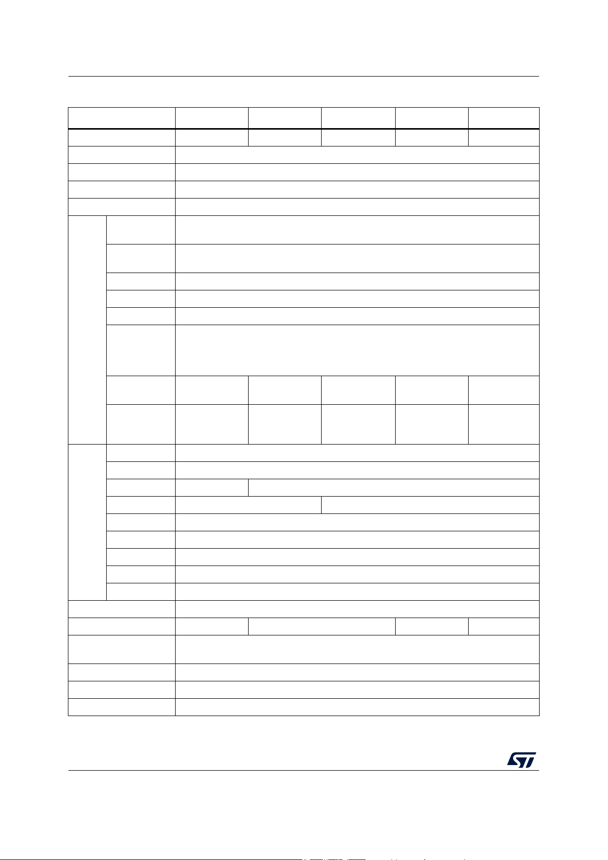
GPIO PORT A
AHB/APB2
USART 2MBps
EXT IT. WKUP
86 AFP
USART 2MBps
GPIO PORT B
PB(15:0)
USART 2MBps
GPIO PORT C
PC(15:0)
USART 2MBps
RX, TX, SCK,CTS,
RTS as AF
USART 2MBps
GPIO PORT D
PD(15:0)
USART 2MBps
GPIO PORT E
PE(15:0)
USART 2MBps
SPI 1
MOSI, MISO
SCK, NSS as AF
APB2 60MHzAPB1
4 CH, ETR as AF
TIMER2
4 CH, ETR as AF
TIMER3&4
RX, TX, SCK,
CTS, RTS as AF
USART2&3
UART4&5
MOSI, MISO, SCK
SPI2&3
NSS, as AF
OUT1/OUT2
DAC1
TIMER6
RTC_OUT
RTC_TS
RTC_TAMPx
OSC_IN
OSC_OUT
VDD, VSS,
VDDA, VSSA,
RESET
VBAT = 1.55 to 3.6V
AHB/APB1
JTAG & SW
Arm
®
Cortex-M4
170 MHz
S-BUS
ETM
MPU
TRACECK
TRACED(3:0)
JTRST, JTDI,
JTCK/SWCLK
JTDO/SWD, JTDO
GP-DMA2
GP-DMA1
8 Chan
FLASH 512 KB
ACCEL/
CACHE
AHB1
@VDDA
POR / BOR
SUPPLY
@VDD
SUPERVISION
Reset
Int
POR
XTAL OSC
4-48MHz
XTAL 32kHz
RTC
AWU
BKPREG
LSI
Standby Interface
IWDG
@VBAT
@VDD
RESET&
CLOCKCTRL
PLL
VDD = 1.71 to 3.6V
VSS
VOLT. REG.
3.3V TO 1.2V
VDD12
POWER MNGT
AHB BUS-MATRIX 5M / 8S
APB2
peripheralclocks
RTC Interface
FPU
WinWATCHDOG
and system
LP timer1
AHB2
SAR ADC2
Ain ADC
SysCfg
CRC
LP_UART1
I2C1&2&3
SCL, SDA, SMBAL as AF
RNG
RNB1
analog
COMP
1,2,3,4
SRAM2 16 KB
PWRCTRL
CAN1&2
FIFO
RX,TX as AF
Vref_Buf
CRS
8 Chan
SRAM1 80 KB
CCM SRAM 16 KB
DMAMUX
HSI
SAR ADC1
IF
@VDDA
16b trigg
TIMER7
16b trigg
USBPD
PHY
CC1
CC2
HSI48
CH2
USB
Device
PHY
D+
D-
FIFO
I2S half
duplex
CH1
OPAMP
1,2,3,6
USART 2MBps
GPIO PORT F
PF(10:9,2:0)
DAC3
CH2
CH1
USART 2MBps
GPIO PORT G
PG(10:10)
CORDIC
FMAC
SAI1
FS, SCK, SD,
MCLK as AF
MSv63469V1
irDA
Smcard
irDA
RX, TX, CTS,
RTS as AF
RX, TX as AF
OSC32_IN
OSC_OUT
@VDDA
NVIC
I-BUS
D-BUS
PVD, PWM
PA(15:0)
TIMER1
16b PWM
TIMER8
16b PWM
USART 2MBps
CH as AF
TIMER15
16b
USART 2MBps
CH as AF
TIMER16
16b
USART 2MBps
TIMER17
CH as AF16b
16b
4 PWM,4PWM,
ETR,BKIN as F
4 PWM,4PWM,
ETR,BKIN as F
USART1
Smcard
irDA
QUADSPI
CLK, NCS, BK1_IO[3:0]
SAR ADC3
IF
TIMER20
16b PWM
4 PWM,4PWM,
ETR,BKIN as F
TinyAES
Description STM32G4A1xE
Figure 1. STM32G4A1xE block diagram
1. AF: alternate function on I/O pins.
16/200 DS13268 Rev 2
Page 17

STM32G4A1xE Functional overview
3 Functional overview
3.1 Arm® Cortex®-M4 core with FPU
The Arm® Cortex®-M4 with FPU processor is the latest generation of Arm processors for
embedded systems. It was developed to provide a low-cost platform that meets the needs of
the MCU implementation, with a reduced pin count and with low-power consumption, while
delivering outstanding computational performance and an advanced response to interrupts.
The Arm
efficiency, delivering the expected high-performance from an Arm core in a memory size
usually associated with 8-bit and 16-bit devices.
The processor supports a set of DSP instructions which allows an efficient signal processing
and a complex algorithm execution. Its single precision FPU speeds up the software
development by using metalanguage development tools to avoid saturation.
With its embedded Arm core, the STM32G4A1xE family is compatible with all Arm tools and
software.
Figure 1 shows the general block diagram of the STM32G4A1xE devices.
®
Cortex®-M4 with FPU 32-bit RISC processor features an exceptional code-
3.2 Adaptive real-time memory accelerator (ART accelerator)
The ART accelerator is a memory accelerator that is optimized for the STM32 industry-
standard Arm
the Arm
processor to wait for the Flash memory at higher frequencies.
®
®
Cortex®-M4 processors. It balances the inherent performance advantage of
Cortex®-M4 over Flash memory technologies, which normally requires the
3.3 Memory protection unit
The memory protection unit (MPU) is used to manage the CPU accesses to the memory
and to prevent one task to accidentally corrupt the memory or the resources used by any
other active task. This memory area is organized into up to 8 protected areas, which can be
divided in up into 8 subareas each. The protection area sizes range between 32 bytes and
the whole 4 gigabytes of addressable memory.
The MPU is especially helpful for applications where some critical or certified code has to be
protected against the misbehavior of other tasks. It is usually managed by an RTOS (real-
time operating system). If a program accesses a memory location that is prohibited by the
MPU, the RTOS can detect it and take action. In an RTOS environment, the kernel can
dynamically update the MPU area setting based on the process to be executed.
The MPU is optional and can be bypassed for applications that do not need it.
3.4 Embedded Flash memory
The STM32G4A1xE devices feature 512 kbytes of embedded Flash memory which is
available for storing programs and data.
Flexible protections can be configured thanks to the option bytes:
DS13268 Rev 2 17/200
45
Page 18

Functional overview STM32G4A1xE
• Readout protection (RDP) to protect the whole memory. Three levels of protection are
available:
– Level 0: no readout protection
– Level 1: memory readout protection; the Flash memory cannot be read from or written
to if either the debug features are connected or the boot in RAM or bootloader are
selected
– Level 2: chip readout protection; the debug features (Cortex-M4 JTAG and serial
wire), the boot in RAM and the bootloader selection are disabled (JTAG fuse). This
selection is irreversible.
• Write protection (WRP): the protected area is protected against erasing and
programming.
• Proprietary code readout protection (PCROP): a part of the Flash memory can be
protected against read and write from third parties. The protected area is execute-only
and it can only be reached by the STM32 CPU as an instruction code, while all other
accesses (DMA, debug and CPU data read, write and erase) are strictly prohibited. An
additional option bit (PCROP_RDP) allows to select if the PCROP area is erased or not
when the RDP protection is changed from Level 1 to Level 0.
• Securable memory area: a part of Flash memory can be configured by option bytes to
be securable. After reset this securable memory area is not secured and it behaves like
the remainder of main Flash memory (execute, read, write access). When secured, any
access to this securable memory area generates corresponding read/write error.
Purpose of the Securable memory area is to protect sensitive code and data (secure
keys storage) which can be executed only once at boot, and never again unless a new
reset occurs.
The Flash memory embeds the error correction code (ECC) feature supporting:
• Single error detection and correction
• Double error detection
• The address of the ECC fail can be read in the ECC register
• 1 Kbyte (128 double word) OTP (one-time programmable) bytes for user data. The
OTP area is available in Bank 1 only. The OTP data cannot be erased and can be
written only once.
3.5 Embedded SRAM
STM32G4A1xE devices feature 112 Kbytes of embedded SRAM. This SRAM is split into
three blocks:
• 80 Kbytes mapped at address 0x2000 0000 (SRAM1). The CM4 can access the
SRAM1 through the System Bus (or through the I-Code/D-Code buses when boot from
SRAM1 is selected or when physical remap is selected by SYSCFG_MEMRMP
register). The first 32 Kbytes of SRAM1 support hardware parity check.
• 16 Kbytes mapped at address 0x2001 4000 (SRAM2). The CM4 can access the
SRAM2 through the System bus. SRAM2 can be kept in stop and standby modes.
• 16 Kbytes mapped at address 0x1000 0000 (CCM SRAM). It is accessed by the CPU
through I-Code/D-Code bus for maximum performance.
It is also aliased at 0x2001 8000 address to be accessed by all masters (CPU, DMA1,
DMA2) through SBUS contiguously to SRAM1 and SRAM2.The CCM SRAM supports
hardware parity check and can be write-protected with 1-Kbyte granularity.
• The memory can be accessed in read/write at max CPU clock speed with 0 wait states.
18/200 DS13268 Rev 2
Page 19
STM32G4A1xE Functional overview
MS52814V1
Cortex
®
-M4
with FPU
DMA1 DMA2
AHB2
peripherals
AHB1
peripherals
CCM
SRAM
SRAM1
FLASH
512 KB
ACCEL
S-bus
D-bus
ICode
DCode
I-bus
BusMatrix-S
SRAM2
QUADSPI
3.6 Multi-AHB bus matrix
The 32-bit multi-AHB bus matrix interconnects all the masters (CPU, DMAs) and the slaves
(Flash memory, RAM, QUADSPI, AHB and APB peripherals). It also ensures a seamless
and efficient operation even when several high-speed peripherals work simultaneously.
Figure 2. Multi-AHB bus matrix
3.7 Boot modes
At startup, a BOOT0 pin (or nBOOT0 option bit)and an nBOOT1 option bit are used to select
one of three boot options:
• Boot from user Flash
• Boot from system memory
• Boot from embedded SRAM
The BOOT0 value may come from the PB8-BOOT0 pin or from an nBOOT0 option bit
depending on the value of a user nBOOT_SEL option bit to free the GPIO pad if needed.
The boot loader is located in the system memory. It is used to reprogram the Flash memory
by using USART, I2C, SPI, and USB through the DFU (device firmware upgrade).
DS13268 Rev 2 19/200
45
Page 20

Functional overview STM32G4A1xE
3.8 CORDIC
The CORDIC provides hardware acceleration of certain mathematical functions, notably
trigonometric, commonly used in motor control, metering, signal processing and many other
applications.
It speeds up the calculation of these functions compared to a software implementation,
allowing a lower operating frequency, or freeing up processor cycles in order to perform
other tasks.
Cordic features
• 24-bit CORDIC rotation engine
• Circular and Hyperbolic modes
• Rotation and Vectoring modes
• Functions: Sine, Cosine, Sinh, Cosh, Atan, Atan2, Atanh, Modulus, Square root,
Natural logarithm
• Programmable precision up to 20-bit
• Fast convergence: 4 bits per clock cycle
• Supports 16-bit and 32-bit fixed point input and output formats
• Low latency AHB slave interface
• Results can be read as soon as ready without polling or interrupt
• DMA read and write channels
3.9 Filter mathematical accelerator (FMAC)
The filter mathematical accelerator unit performs arithmetic operations on vectors. It
comprises a multiplier/accumulator (MAC) unit, together with address generation logic,
which allows it to index vector elements held in local memory.
The unit includes support for circular buffers on input and output, which allows digital filters
to be implemented. Both finite and infinite impulse response filters can be realized.
The unit allows frequent or lengthy filtering operations to be offloaded from the CPU, freeing
up the processor for other tasks. In many cases it can accelerate such calculations
compared to a software implementation, resulting in a speed-up of time critical tasks.
20/200 DS13268 Rev 2
Page 21

STM32G4A1xE Functional overview
FMAC features
• 16 x 16-bit multiplier
• 24+2-bit accumulator with addition and subtraction
• 16-bit input and output data
• 256 x 16-bit local memory
• Up to three areas can be defined in memory for data buffers (two input, one output),
defined by programmable base address pointers and associated size registers
• Input and output sample buffers can be circular
• Buffer “watermark” feature reduces overhead in interrupt mode
• Filter functions: FIR, IIR (direct form 1)
• AHB slave interface
• DMA read and write data channels
3.10 Cyclic redundancy check calculation unit (CRC)
The CRC (cyclic redundancy check) calculation unit is used to get a CRC code using a
configurable generator with polynomial value and size.
Among other applications, the CRC-based techniques are used to verify data transmission
or storage integrity. In the scope of the EN/IEC 60335-1 standard, they offer a mean to verify
the Flash memory integrity.
The CRC calculation unit helps to compute a signature of the software during runtime, which
can be ulteriorly compared with a reference signature generated at link-time and which can
be stored at a given memory location.
3.11 Power supply management
3.11.1 Power supply schemes
The STM32G4A1xE devices require a 1.71 V to 3.6 V V
Several independent supplies, can be provided for specific peripherals:
• V
• V
• V
= 1.71 V to 3.6 V
DD
V
is the external power supply for the I/Os, the internal regulator and the system
DD
analog such as reset, power management and internal clocks. It is provided externally
through the VDD pins.
= 1.62 V to 3.6 V (see Section 5: Electrical characteristics for the minimum V
DDA
voltage required for ADC, DAC, COMP, OPAMP, VREFBUF operation).
V
is the external analog power supply for A/D converters, D/A converters, voltage
DDA
reference buffer, operational amplifiers and comparators. The V
independent from the V
voltage and should preferably be connected to VDD when
DD
these peripherals are not used.
= 1.55 V to 3.6 V
BAT
V
is the power supply for RTC, external clock 32 kHz oscillator and backup registers
BAT
(through power switch) when V
is not present.
DD
operating voltage supply.
DD
voltage level is
DDA
DDA
DS13268 Rev 2 21/200
45
Page 22

Functional overview STM32G4A1xE
• VREF-, VREF+
V
is the input reference voltage for ADCs and DACs. It is also the output of the
REF+
internal voltage reference buffer when enabled.
When V
When V
DDA
DDA
< 2 V V
2 V V
must be equal to V
REF+
must be between 2 V and V
REF+
DDA
.
.
DDA
The internal voltage reference buffer supports three output voltages, which are
configured with VRS bits in the VREFBUF_CSR register:
–V
–V
–V
V
REF-
= 2.048 V
REF+
= 2.5 V
REF+
= 2.9 V
REF+
is double bonded with V
SSA
.
3.11.2 Power supply supervisor
The device has an integrated ultra-low-power brown-out reset (BOR) active in all modes
(except for Shutdown mode). The BOR ensures proper operation of the device after poweron and during power down. The device remains in reset mode when the monitored supply
voltage V
The lowest BOR level is 1.71 V at power on, and other higher thresholds can be selected
through option bytes.The device features an embedded programmable voltage detector
(PVD) that monitors the V
interrupt can be generated when V
higher than the VPVD threshold. The interrupt service routine can then generate a warning
message and/or put the MCU into a safe state. The PVD is enabled by software.
is below a specified threshold, without the need for an external reset circuit.
DD
power supply and compares it to the VPVD threshold. An
DD
drops below the VPVD threshold and/or when VDD is
DD
In addition, the device embeds a peripheral voltage monitor which compares the
independent supply voltages V
peripheral is in its functional supply range.
3.11.3 Voltage regulator
Two embedded linear voltage regulators, main regulator (MR) and low-power regulator
(LPR), supply most of digital circuitry in the device. The MR is used in Run and Sleep
modes. The LPR is used in Low-power run, Low-power sleep and Stop modes. In Standby
and Shutdown modes, both regulators are powered down and their outputs set in highimpedance state, such as to bring their current consumption close to zero.
The device supports dynamic voltage scaling to optimize its power consumption in Run
mode. the voltage from the main regulator that supplies the logic (VCORE) can be adjusted
according to the system’s maximum operating frequency.
The main regulator (MR) operates in the following ranges:
• Range 1 boost mode with the CPU running at up to 170 MHz.
• Range 1 normal mode with CPU running at up to 150 MHz.
• Range 2 with a maximum CPU frequency of 26 MHz.
, with a fixed threshold in order to ensure that the
DDA
22/200 DS13268 Rev 2
Page 23

STM32G4A1xE Functional overview
3.11.4 Low-power modes
By default, the microcontroller is in Run mode after system or power Reset. It is up to the
user to select one of the low-power modes described below:
• Sleep mode: In Sleep mode, only the CPU is stopped. All peripherals continue to
operate and can wake up the CPU when an interrupt/event occurs.
• Low-power run mode: This mode is achieved with VCORE supplied by the low-power
regulator to minimize the regulator's operating current. The code can be executed from
SRAM or from Flash, and the CPU frequency is limited to 2 MHz. The peripherals with
independent clock can be clocked by HSI16.
• Stop mode: In Stop mode, the device achieves the lowest power consumption while
retaining the SRAM and register contents. All clocks in the VCORE domain are
stopped. The PLL, as well as the HSI16 RC oscillator and the HSE crystal oscillator are
disabled. The LSE or LSI keep running. The RTC can remain active (Stop mode with
RTC, Stop mode without RTC). Some peripherals with wakeup capability can enable
the HSI16 RC during Stop mode, so as to get clock for processing the wakeup event.
• Standby mode: The Standby mode is used to achieve the lowest power consumption
with brown-out reset, BOR. The internal regulator is switched off to power down the
VCORE domain. The PLL, as well as the HSI16 RC oscillator and the HSE crystal
oscillator are also powered down. The RTC can remain active (Standby mode with
RTC, Standby mode without RTC). The BOR always remains active in Standby mode.
For each I/O, the software can determine whether a pull-up, a pull-down or no resistor
shall be applied to that I/O during Standby mode. Upon entering Standby mode, SRAM
and register contents are lost except for registers in the RTC domain and standby
circuitry. The device exits Standby mode upon external reset event (NRST pin), IWDG
reset event, wakeup event (WKUP pin, configurable rising or falling edge) or RTC
event (alarm, periodic wakeup, timestamp, tamper), or when a failure is detected on
LSE (CSS on LSE).
• Shutdown mode: The Shutdown mode allows to achieve the lowest power
consumption. The internal regulator is switched off to power down the VCORE domain.
The PLL, as well as the HSI16 and LSI RC-oscillators and HSE crystal oscillator are
also powered down. The RTC can remain active (Shutdown mode with RTC, Shutdown
mode without RTC). The BOR is not available in Shutdown mode. No power voltage
monitoring is possible in this mode. Therefore, switching to RTC domain is not
supported. SRAM and register contents are lost except for registers in the RTC
domain. The device exits Shutdown mode upon external reset event (NRST pin),
IWDG reset event, wakeup event (WKUP pin, configurable rising or falling edge) or
RTC event (alarm, periodic wakeup, timestamp, tamper).
3.11.5 Reset mode
In order to improve the consumption under reset, the I/Os state under and after reset is
“analog state” (the I/O schmitt trigger is disabled). In addition, the internal reset pull-up is
deactivated when the reset source is internal.
3.11.6 V
operation
BAT
The V
pin allows to power the device V
BAT
supercapacitor, or from V
supercapacitor is present. The V
registers. Three anti-tamper detection pins are available in V
domain from an external battery, an external
when there is no external battery and when an external
DD
BAT
DS13268 Rev 2 23/200
BAT
pin supplies the RTC with LSE and the backup
mode.
BAT
45
Page 24

Functional overview STM32G4A1xE
The V
operation is automatically activated when VDD is not present. An internal V
BAT
battery charging circuit is embedded and can be activated when V
Note: When the microcontroller is supplied from V
alarm/events exit the microcontroller from the V
is present.
DD
, neither external interrupts nor RTC
BAT
operation.
BAT
BAT
24/200 DS13268 Rev 2
Page 25
STM32G4A1xE Functional overview
3.12 Interconnect matrix
Several peripherals have direct connections between them. This allows autonomous
communication between peripherals, saving CPU resources thus power supply
consumption. In addition, these hardware connections allow fast and predictable latency.
Depending on peripherals, these interconnections can operate in Run, Sleep and Stop
modes.
Table 3. STM32G4A1xE peripherals interconnect matrix
Interconnect source
TIMx
TIM16/TIM17 IRTIM Infrared interface output generation Y Y Y -
COMPx
ADCx TIM1, 8, 20 Timer triggered by analog watchdog Y Y Y -
RTC
All clocks sources (internal
and external)
USB TIM2 Timer triggered by USB SOF Y Y - -
CSS
CPU (hard fault)
RAM (parity error)
Flash memory (ECC error)
COMPx
PVD
Interconnect
destination
TIMx Timers synchronization or chaining Y Y Y -
ADCx
DACx
DMA Memory to memory transfer trigger Y Y Y -
COMPx Comparator output blanking Y Y Y -
TIM1, 8, 20
TIM2, 3, 4
LPTIMER1
TIM16
LPTIMER1
TIM15, 16, 17
TIM1, 8, 20
TIM15, 16, 17
TIMx External trigger Y Y Y -
Conversion triggers Y Y Y -
Timer input channel, trigger, break
from analog signals comparison
Low-power timer triggered by
analog signals comparison
Timer input channel from RTC
events
Low-power timer triggered by RTC
alarms or tampers
Clock source used as input channel
for RC measurement and trimming
Timer break Y Y Y -
Interconnect action
Run
Sleep
Low-power run
YYY -
YYYY
YYY -
YYYY
YYY -
Stop
GPIO
LPTIMER1 External trigger Y Y Y -
ADCx
DACx
DS13268 Rev 2 25/200
Conversion external trigger Y Y Y -
45
Page 26

Functional overview STM32G4A1xE
3.13 Clocks and startup
The clock controller distributes the clocks coming from different oscillators to the core and
the peripherals. It also manages clock gating for low-power modes and ensures clock
robustness. It features:
• Clock prescaler: to get the best trade-off between speed and current consumption,
the clock frequency to the CPU and peripherals can be adjusted by a programmable
prescaler
• Safe clock switching: clock sources can be changed safely on the fly in run mode
through a configuration register.
• Clock management: to reduce power consumption, the clock controller can stop the
clock to the core, individual peripherals or memory.
• System clock source: three different sources can deliver SYSCLK system clock:
– 4 - 48 MHz high-speed oscillator with external crystal or ceramic resonator (HSE).
It can supply clock to system PLL. The HSE can also be configured in bypass
mode for an external clock.
– 16 MHz high-speed internal RC oscillator (HSI16), trimmable by software. It can
supply clock to system PLL.
– System PLL with maximum output frequency of 170 MHz. It can be fed with HSE
or HSI16 clocks.
• RC48 with clock recovery system (HSI48): internal HSIRC48 MHz clock source can
be used to drive the USB or the RNG peripherals.
• Auxiliary clock source: two ultra-low-power clock sources for the real-time clock
(RTC):
– 32.768 kHz low-speed oscillator with external crystal (LSE), supporting four drive
capability modes. The LSE can also be configured in bypass mode for using an
external clock.
– 32 kHz low-speed internal RC oscillator (LSI) with ±5% accuracy, also used to
clock an independent watchdog.
• Peripheral clock sources: several peripherals (I2S, USART, I2C, LPTimer, ADC, SAI,
RNG) have their own clock independent of the system clock.
• Clock security system (CSS): in the event of HSE clock failure, the system clock is
automatically switched to HSI16 and, if enabled, a software interrupt is generated. LSE
clock failure can also be detected and generate an interrupt.
• Clock-out capability:
– MCO: microcontroller clock output: it outputs one of the internal clocks for external
use by the application
– LSCO: low speed clock output: it outputs LSI or LSE in all low-power modes.
Several prescalers allow to configure the AHB frequency, the High-speed APB (APB2) and
the low speed APB (APB1) domains. The maximum frequency of the AHB and the APB
domains is 170 MHz.
26/200 DS13268 Rev 2
Page 27

STM32G4A1xE Functional overview
3.14 General-purpose inputs/outputs (GPIOs)
Each of the GPIO pins can be configured by software as output (push-pull or open-drain), as
input (with or without pull-up or pull-down) or as peripheral alternate function. Most of the
GPIO pins are shared with digital or analog alternate functions. Fast I/O toggling can be
achieved thanks to their mapping on the AHB2 bus.
The I/Os alternate function configuration can be locked if needed following a specific
sequence in order to avoid spurious writing to the I/Os registers.
3.15 Direct memory access controller (DMA)
The device embeds 2 DMAs. Refer to Table 4: DMA implementation for the features
implementation.
Direct memory access (DMA) is used in order to provide a high-speed data transfer
between peripherals and memory as well as from memory to memory. Data can be quickly
moved by DMA without any CPU actions. This keeps the CPU resources free for other
operations.
The two DMA controllers have 16 channels in total, each one dedicated to manage memory
access requests from one or more peripherals. Each controller has an arbiter for handling
the priority between DMA requests.
The DMA supports:
• 16 independently configurable channels (requests)
– Each channel is connected to a dedicated hardware DMA request, a software
trigger is also supported on each channel. This configuration is done by software.
• Priorities between requests from channels of one DMA are both software
programmable (4 levels: very high, high, medium, low) or hardware programmable in
case of equality (request 1 has priority over request 2, etc.)
• Independent source and destination transfer size (byte, half word, word), emulating
packing and unpacking. Source/destination addresses must be aligned on the data
size.
• Support for circular buffer management
• 3 event flags (DMA half transfer, DMA transfer complete and DMA transfer error)
logically ORed together in a single interrupt request for each channel
• Memory-to-memory transfer
• Peripheral-to-memory, memory-to-peripheral, and peripheral-to-peripheral transfers
• Access to Flash, SRAM, APB and AHB peripherals as source and destination
• Programmable number of data to be transferred: up to 65536.
DMA features DMA1 DMA2
Number of regular channels 8 8
Table 4. DMA implementation
DS13268 Rev 2 27/200
45
Page 28

Functional overview STM32G4A1xE
3.16 DMA request router (DMAMux)
When a peripheral indicates a request for DMA transfer by setting its DMA request line, the
DMA request is pending until it is served and the corresponding DMA request line is reset.
The DMA request router allows to route the DMA control lines between the peripherals and
the DMA controllers of the product.
An embedded multi-channel DMA request generator can be considered as one of such
peripherals. The routing function is ensured by a multi-channel DMA request line
multiplexer. Each channel selects a unique set of DMA control lines, unconditionally or
synchronously with events on synchronization inputs.
For simplicity, the functional description is limited to DMA request lines. The other DMA
control lines are not shown in figures or described in the text. The DMA request generator
produces DMA requests following events on DMA request trigger inputs.
3.17 Interrupts and events
3.17.1 Nested vectored interrupt controller (NVIC)
The STM32G4A1xE devices embed a nested vectored interrupt controller which is able to
manage 16 priority levels, and to handle up to 71 maskable interrupt channels plus the 16
interrupt lines of the Cortex
®
-M4.
The NVIC benefits are the following:
• Closely coupled NVIC gives low latency interrupt processing
• Interrupt entry vector table address passed directly to the core
• Allows early processing of interrupts
• Processing of late arriving higher priority interrupts
• Support for tail chaining
• Processor state automatically saved
• Interrupt entry restored on interrupt exit with no instruction overhead
The NVIC hardware block provides flexible interrupt management features with minimal
interrupt latency.
3.17.2 Extended interrupt/event controller (EXTI)
The extended interrupt/event controller consists of 40 edge detector lines used to generate
interrupt/event requests and to wake-up the system from the Stop mode. Each external line
can be independently configured to select the trigger event (rising edge, falling edge, both)
and can be masked independently.
A pending register maintains the status of the interrupt requests. The internal lines are
connected to peripherals with wakeup from Stop mode capability. The EXTI can detect an
external line with a pulse width shorter than the internal clock period. Up to 86 GPIOs can
be connected to the 16 external interrupt lines.
28/200 DS13268 Rev 2
Page 29

STM32G4A1xE Functional overview
3.18 Analog-to-digital converter (ADC)
The device embeds three successive approximation analog-to-digital converters with the
following features:
• 12-bit native resolution, with built-in calibration
• 4 Msps maximum conversion rate with full resolution
– Down to 41.67 ns sampling time
– Increased conversion rate for lower resolution (up to 6.66 Msps for 6-bit
resolution)
• One external reference pin is available on all packages, allowing the input voltage
range to be independent from the power supply
• Single-ended and differential mode inputs
• Low-power design
– Capable of low-current operation at low conversion rate (consumption decreases
linearly with speed)
– Dual clock domain architecture: ADC speed independent from CPU frequency
• Highly versatile digital interface
– Single-shot or continuous/discontinuous sequencer-based scan mode: 2 groups
of analog signals conversions can be programmed to differentiate background and
high-priority real-time conversions
– Each ADC support multiple trigger inputs for synchronization with on-chip timers
and external signals
– Results stored into a data register or in RAM with DMA controller support
– Data pre-processing: left/right alignment and per channel offset compensation
– Built-in oversampling unit for enhanced SNR
– Channel-wise programmable sampling time
– Analog watchdog for automatic voltage monitoring, generating interrupts and
trigger for selected timers
– Hardware assistant to prepare the context of the injected channels to allow fast
context switching
– Flexible sample time control
– Hardware gain and offset compensation
3.18.1 Temperature sensor
The temperature sensor (TS) generates a voltage VTS that varies linearly with temperature.
The temperature sensor is internally connected to the ADC1_IN16 input channel which is
used to convert the sensor output voltage into a digital value.
The sensor provides good linearity but it has to be calibrated to obtain good overall
accuracy of the temperature measurement. As the offset of the temperature sensor varies
from chip to chip due to process variation, the uncalibrated internal temperature sensor is
suitable for applications that detect temperature changes only.
To improve the accuracy of the temperature sensor measurement, each device is
individually factory-calibrated by ST. The temperature sensor factory calibration data are
stored by ST in the system memory area, accessible in read-only mode.
DS13268 Rev 2 29/200
45
Page 30
Functional overview STM32G4A1xE
Calibration value name Description Memory address
TS_CAL1
TS_CAL2
Table 5. Temperature sensor calibration values
TS ADC raw data acquired at a
temperature of 30 °C (± 5 °C),
V
DDA
TS ADC raw data acquired at a
temperature of 110 °C (± 5 °C),
V
DDA
3.18.2 Internal voltage reference (V
The internal voltage reference (VREFINT) provides a stable (bandgap) voltage output for
the ADC and the comparators. The VREFINT is internally connected to the ADC1_IN18 and
ADC3_IN18 input channel. The precise voltage of VREFINT is individually measured for
each part by ST during production test and stored in the system memory area. It is
accessible in read-only mode.
Calibration value name Description Memory address
Table 6. Internal voltage reference calibration values
Raw data acquired at a
VREFINT
temperature of 30 °C (± 5 °C),
V
DDA
= V
REF+
= V
REF+
REFINT
= V
REF+
0x1FFF 75A8 - 0x1FFF 75A9
= 3.0 V (± 10 mV)
0x1FFF 75CA - 0x1FFF 75CB
= 3.0 V (± 10 mV)
)
0x1FFF 75AA - 0x1FFF 75AB
= 3.0 V (± 10 mV)
3.18.3 V
battery voltage monitoring
BAT
This embedded hardware enables the application to measure the V
the internal ADC1_IN17 channel. As the V
voltage may be higher than the V
BAT
thus outside the ADC input range, the VBAT pin is internally connected to a bridge divider by
3. As a consequence, the converted digital value is one third of the V
3.18.4 Operational amplifier internal output (OPAMPxINT):
The OPAMPx (x = 1,2,3,6) output OPAMPxINT can be sampled using an ADCx (x = 1,2,3)
internal input channel. In this case, the I/O on which the OPAMPx output is mapped can be
used as GPIO.
3.19 Digital to analog converter (DAC)
Four 12 bit DAC channels (2 external buffered and 2 internal unbuffered) can be used to
convert digital signals into analog voltage signal outputs. The chosen design structure is
composed of integrated resistor strings and an amplifier in inverting configuration.
battery voltage using
BAT
DDA
voltage.
BAT
, and
30/200 DS13268 Rev 2
Page 31

STM32G4A1xE Functional overview
MSv40197V1
VREFBUF
Low frequency
cut-off capacitor
DAC, ADC
Bandgap +
V
DDA
-
100 nF
VREF+
This digital interface supports the following features:
• Up to two DAC output channels
• 8-bit or 12-bit output mode
• Buffer offset calibration (factory and user trimming)
• Left or right data alignment in 12-bit mode
• Synchronized update capability
• Noise-wave generation
• Triangular-wave generation
• Saw tooth wave generation
• Dual DAC channel independent or simultaneous conversions
• DMA capability for each channel
• External triggers for conversion
• Sample and hold low-power mode, with internal or external capacitor
• Up to 1 Msps for external output and 15 Msps for internal output
The DAC channels are triggered through the timer update outputs that are also connected
to different DMA channels.
3.20 Voltage reference buffer (V
The STM32G4A1xE devices embed a voltage reference buffer which can be used as
voltage reference for ADC, DACs and also as voltage reference for external components
through the VREF+ pin.
The internal voltage reference buffer supports three voltages:
• 2.048 V
• 2.5 V
• 2.9 V
An external voltage reference can be provided through the VREF+ pin when the internal
voltage reference buffer is off.
The VREF+ pin is double-bonded with V
internal voltage reference buffer is not available.
Figure 3. Voltage reference buffer
REFBUF
DDA
)
on some packages. In these packages the
DS13268 Rev 2 31/200
45
Page 32

Functional overview STM32G4A1xE
3.21 Comparators (COMP)
The STM32G4A1xE devices embed four rail-to-rail comparators with programmable
reference voltage (internal or external), hysteresis.
The reference voltage can be one of the following:
• External I/O
• DAC output channels
• Internal reference voltage or submultiple (1/4, 1/2, 3/4).
All comparators can wake up from Stop mode, generate interrupts and breaks for the timers.
3.22 Operational amplifier (OPAMP)
The STM32G4A1xE devices embed four operational amplifiers (OPAMP1, OPAMP2,
OPAMP3, OPAMP6) with external or internal follower routing and PGA capability.
The operational amplifier features:
• 13 MHz bandwidth
• Rail-to-rail input/output
• PGA with a non-inverting gain ranging of 2, 4, 8, 16, 32 or 64 or inverting gain ranging
of -1, -3, -7, -15, -31 or -63
3.23 Random number generator (RNG)
All devices embed an RNG that delivers 32-bit random numbers generated by an integrated
analog circuit.
3.24 Advanced encryption standard hardware accelerator (AES)
The STM32G4A1xE devices embed an AES hardware accelerator that can be used both to
encipher and to decipher data using an AES algorithm.
32/200 DS13268 Rev 2
Page 33

STM32G4A1xE Functional overview
The AES peripheral supports:
• Encryption/decryption using AES Rijndael block cipher algorithm
• NIST FIPS 197 compliant implementation of AES encryption/decryption algorithm
• 128-bit and 256-bit register for storing the encryption, decryption or derivation key (4x
32-bit registers)
• Electronic codebook (ECB), cipher block chaining (CBC), Counter mode (CTR), Galois
Counter Mode (GCM), Galois Message Authentication Code mode (GMAC) and Cipher
Message Authentication Code mode (CMAC) supported
• Key scheduler
• Key derivation for decryption
• 128-bit data block processing
• 128-bit, 256-bit key length
• 1x32-bit INPUT buffer and 1x32-bit OUTPUT buffer
• Register access supporting 32-bit data width only
• One 128-bit Register for the initialization vector when AES is configured in CBC mode
or for the 32-bit counter initialization when CTR mode is selected, GCM mode or
CMAC mode
• Automatic data flow control with support of direct memory access (DMA) using 2
channels, one for incoming data, and one for outcoming data
• Suspend a message if another message with a higher priority needs to be processed.
3.25 Timers and watchdogs
The STM32G4A1xE devices include three advanced motor control timers, up to six generalpurpose timers, two basic timers, one low-power timer, two watchdog timers and a SysTick
timer. The table below compares the features of the advanced motor control, general
purpose and basic timers.
Timer type Timer
Advanced
motor
control
General-
purpose
General-
purpose
General-
purpose
TIM1, TIM8,
TIM20
TIM2 32-bit
TIM3, TIM4 16-bit
TIM15 16-bit Up
Table 7. Timer feature comparison
Counter
resolution
16-bit
Counter
type
Up,
down,
Up/down
Up,
down,
Up/down
Up,
down,
Up/down
Prescaler
factor
Any integer
between 1 and
65536
Any integer
between 1 and
65536
Any integer
between 1 and
65536
Any integer
between 1 and
65536
DMA
request
generation
Yes 4 4
Yes 4 No
Yes 4 No
Yes 2 1
Capture/
compare
channels
Complementary
outputs
DS13268 Rev 2 33/200
45
Page 34

Functional overview STM32G4A1xE
Table 7. Timer feature comparison (continued)
Timer type Timer
General-
purpose
Basic TIM6, TIM7 16-bit Up
TIM16, TIM17 16-bit Up
Counter
resolution
Counter
type
Prescaler
factor
Any integer
between 1 and
65536
Any integer
between 1 and
65536
DMA
request
generation
Yes 1 1
Yes 0 No
3.25.1 Advanced motor control timer (TIM1, TIM8, TIM20)
The advanced motor control timers can each be seen as a four-phase
PWM multiplexed on 8 channels. They have complementary PWM outputs with
programmable inserted dead-times. They can also be seen as complete general-purpose
timers.
The 4 independent channels can be used for:
• Input capture
• Output compare
• PWM generation (edge or center-aligned modes) with full modulation capability
(0-100%)
• One-pulse mode output
Capture/
compare
channels
Complementary
outputs
In debug mode, the advanced motor control timer counter can be frozen and the PWM
outputs disabled in order to turn off any power switches driven by these outputs.
Many features are shared with the general-purpose TIMx timers (described in
Section 3.25.2) using the same architecture, so the advanced motor control timers can work
together with the TIMx timers via the Timer Link feature for synchronization or event
chaining.
34/200 DS13268 Rev 2
Page 35

STM32G4A1xE Functional overview
3.25.2 General-purpose timers (TIM2, TIM3, TIM4, TIM15, TIM16, TIM17)
There are up to six synchronizable general-purpose timers embedded in the
STM32G4A1xE devices (see Tab l e 7 for differences). Each general-purpose timer can be
used to generate PWM outputs, or act as a simple time base.
• TIM2, TIM3, and TIM4
They are full-featured general-purpose timers:
– TIM2 has a 32-bit auto-reload up/downcounter and 32-bit prescaler
– TIM3 and TIM4 have 16-bit auto-reload up/downcounter and 16-bit prescaler.
These timers feature 4 independent channels for input capture/output compare, PWM
or one-pulse mode output. They can work together, or with the other general-purpose
timers via the Timer Link feature for synchronization or event chaining.
The counters can be frozen in debug mode.
All have independent DMA request generation and support quadrature encoders.
• TIM15, 16 and 17
They are general-purpose timers with mid-range features:
They have 16-bit auto-reload upcounters and 16-bit prescalers.
– TIM15 has 2 channels and 1 complementary channel
– TIM16 and TIM17 have 1 channel and 1 complementary channel
All channels can be used for input capture/output compare, PWM or one-pulse mode
output.
The timers can work together via the Timer Link feature for synchronization or event
chaining. The timers have independent DMA request generation.
The counters can be frozen in debug mode.
3.25.3 Basic timers (TIM6 and TIM7)
The basic timers are mainly used for DAC trigger generation. They can also be used as
generic 16-bit timebases.
DS13268 Rev 2 35/200
45
Page 36

Functional overview STM32G4A1xE
3.25.4 Low-power timer (LPTIM1)
The devices embed a low-power timer. This timer has an independent clock and are running
in Stop mode if it is clocked by LSE, LSI or an external clock. It is able to wakeup the system
from Stop mode.
LPTIM1 is active in Stop mode.
This low-power timer supports the following features:
• 16-bit up counter with 16-bit autoreload register
• 16-bit compare register
• Configurable output: pulse, PWM
• Continuous/ one shot mode
• Selectable software/hardware input trigger
• Selectable clock source
– Internal clock sources: LSE, LSI, HSI16 or APB clock
– External clock source over LPTIM input (working even with no internal clock
source running, used by pulse counter application).
• Programmable digital glitch filter
• Encoder mode
3.25.5 Independent watchdog (IWDG)
The independent watchdog is based on a 12-bit downcounter and an 8-bit prescaler. It is
clocked from an independent 32 kHz internal RC (LSI) and as it operates independently
from the main clock, it can operate in Stop and Standby modes. It can be used either as a
watchdog to reset the device when a problem occurs, or as a free running timer for
application timeout management. It is hardware or software configurable through the option
bytes. The counter can be frozen in debug mode.
3.25.6 System window watchdog (WWDG)
The window watchdog is based on a 7-bit downcounter that can be set as free running. It
can be used as a watchdog to reset the device when a problem occurs. It is clocked from
the main clock. It has an early warning interrupt capability and the counter can be frozen in
debug mode.
3.25.7 SysTick timer
This timer is dedicated to real-time operating systems, but could also be used as a standard
down counter. It features:
• A 24-bit down counter
• Autoreload capability
• Maskable system interrupt generation when the counter reaches 0.
• Programmable clock source
36/200 DS13268 Rev 2
Page 37

STM32G4A1xE Functional overview
3.26 Real-time clock (RTC) and backup registers
The RTC supports the following features:
• Calendar with subsecond, seconds, minutes, hours (12 or 24 format), week day, date,
month, year, in BCD (binary-coded decimal) format.
• Automatic correction for 28, 29 (leap year), 30, and 31 days of the month.
• Two programmable alarms.
• On-the-fly correction from 1 to 32767 RTC clock pulses. This can be used to
synchronize it with a master clock.
• Reference clock detection: a more precise second source clock (50 or 60 Hz) can be
used to enhance the calendar precision.
• Digital calibration circuit with 0.95 ppm resolution, to compensate for quartz crystal
inaccuracy.
• Timestamp feature which can be used to save the calendar content. This function can
be triggered by an event on the timestamp pin, or by a tamper event, or by a switch to
V
mode.
BAT
• 17-bit auto-reload wakeup timer (WUT) for periodic events with programmable
resolution and period.
The RTC is supplied through a switch that takes power either from the V
present or from the VBAT pin.
The RTC clock sources can be:
• A 32.768 kHz external crystal (LSE)
• An external resonator or oscillator (LSE)
• The internal low power RC oscillator (LSI, with typical frequency of 32 kHz)
• The high-speed external clock (HSE) divided by 32.
The RTC is functional in V
mode and in all low-power modes when it is clocked by the
BAT
LSE. When clocked by the LSI, the RTC is not functional in V
all low-power modes except Shutdown mode.
All RTC events (Alarm, WakeUp Timer, Timestamp) can generate an interrupt and wakeup
the device from the low-power modes.
3.27 Tamper and backup registers (TAMP)
• 32 32-bit backup registers, retained in all low-power modes and also in V
They can be used to store sensitive data as their content is protected by an tamper
detection circuit. They are not reset by a system or power reset, or when the device
wakes up from Standby or Shutdown mode.
• Up to three tamper pins for external tamper detection events. The external tamper pins
can be configured for edge detection, edge and level, level detection with filtering.
• Five internal tampers events.
• Any tamper detection can generate a RTC timestamp event.
• Any tamper detection erases the backup registers.
• Any tamper detection can generate an interrupt and wake-up the device from all low-
power modes.
supply when
DD
mode, but is functional in
BAT
mode.
BAT
DS13268 Rev 2 37/200
45
Page 38

Functional overview STM32G4A1xE
3.28 Infrared transmitter
The STM32G4A1xE devices provide an infrared transmitter solution. The solution is based
on internal connections between TIM16 and TIM17 as shown in the figure below.
TIM17 is used to provide the carrier frequency and TIM16 provides the main signal to be
sent. The infrared output signal is available on PB9 or PA13.
To generate the infrared remote control signals, TIM16 channel 1 and TIM17 channel 1 must
be properly configured to generate correct waveforms. All standard IR pulse modulation
modes can be obtained by programming the two timers output compare channels.
Figure 4. Infrared transmitter
TIM17_CH1
TIM16_CH1
IRTIM
IR_OUT
MS30474V2
38/200 DS13268 Rev 2
Page 39

STM32G4A1xE Functional overview
3.29 Inter-integrated circuit interface (I2C)
The device embeds three I2Cs. Refer to Table 8: I2C implementation for the features
implementation.
2
The I
C bus interface handles communications between the microcontroller and the serial
2
I
C bus. It controls all I2C bus-specific sequencing, protocol, arbitration and timing.
The I2C peripheral supports:
2
• I
C-bus specification and user manual rev. 5 compatibility:
– Slave and master modes, multimaster capability
– Standard-mode (Sm), with a bitrate up to 100 kbit/s
– Fast-mode (Fm), with a bitrate up to 400 kbit/s
– Fast-mode Plus (Fm+), with a bitrate up to 1 Mbit/s and 20 mA output drive I/Os
– 7-bit and 10-bit addressing mode, multiple 7-bit slave addresses
– Programmable setup and hold times
– Optional clock stretching
• System management bus (SMBus) specification rev 2.0 compatibility:
– Hardware PEC (packet error checking) generation and verification with ACK
control
– Address resolution protocol (ARP) support
– SMBus alert
• Power system management protocol (PMBus
• Independent clock: a choice of independent clock sources allowing the I2C
communication speed to be independent from the PCLK reprogramming.
• Wakeup from Stop mode on address match
• Programmable analog and digital noise filters
• 1-byte buffer with DMA capability
Table 8. I2C implementation
I2C features
(1)
TM
) specification rev 1.1 compatibility
I2C1 I2C2 I2C3
Standard-mode (up to 100 kbit/s) X X X
Fast-mode (up to 400 kbit/s) X X X
Fast-mode Plus with 20mA output drive I/Os (up to 1 Mbit/s) X X X
Programmable analog and digital noise filters X X X
SMBus/PMBus hardware support X X X
Independent clock X X X
Wakeup from Stop mode on address match X X X
1. X: supported
DS13268 Rev 2 39/200
45
Page 40

Functional overview STM32G4A1xE
3.30 Universal synchronous/asynchronous receiver transmitter (USART)
The STM32G4A1xE devices have three embedded universal synchronous receiver
transmitters (USART1, USART2 and USART3) and two universal asynchronous receiver
transmitters (UART4, UART5).
These interfaces provide asynchronous communication, IrDA SIR ENDEC support,
multiprocessor communication mode, single-wire half-duplex communication mode and
have LIN master/slave capability. They provide hardware management of the CTS and RTS
signals, and RS485 driver enable.
The USART1, USART2 and USART3 also provide a Smartcard mode (ISO 7816 compliant)
and an SPI-like communication capability.
The USART comes with a Transmit FIFO (TXFIFO) and a Receive FIFO (RXFIFO). FIFO
mode is enabled by software and is disabled by default.
All USART have a clock domain independent from the CPU clock, allowing the USARTx
(x=1,2,3,4) to wake up the MCU from Stop mode. The wakeup from Stop mode can be done
on:
• Start bit detection
• Any received data frame
• A specific programmed data frame
• Some specific TXFIFO/RXFIFO status interrupts when FIFO mode is enabled
All USART interfaces can be served by the DMA controller.
USART modes/features
Hardware flow control for modem XXXXX X
Continuous communication using DMA XXXXX X
Multiprocessor communication XXXXX X
Synchronous mode X X X - - -
Smartcard mode X X X - - -
Single-wire half-duplex communication XXXXX X
IrDA SIR ENDEC block XXXXX -
LIN mode XXXXX -
Dual clock domain XXXXX X
Wakeup from Stop mode XXXXX X
Receiver timeout interrupt XXXXX -
Modbus communication XXXXX -
Auto baud rate detection X (4 modes) -
Driver Enable XXXXX X
LPUART/USART data length 7, 8 and 9 bits
Table 9. USART/UART/LPUART features
(1)
USART1 USART2 USART3 UART4 UART5 LPUART1
40/200 DS13268 Rev 2
Page 41

STM32G4A1xE Functional overview
Table 9. USART/UART/LPUART features (continued)
USART modes/features
Tx/Rx FIFO X
Tx/Rx FIFO size 8
1. X = supported.
(1)
USART1 USART2 USART3 UART4 UART5 LPUART1
3.31 Low-power universal asynchronous receiver transmitter (LPUART)
The STM32G4A1xE devices embed one Low-Power UART. The LPUART supports
asynchronous serial communication with minimum power consumption. It supports halfduplex single-wire communication and modem operations (CTS/RTS). It allows
multiprocessor communication.
The LPUART comes with a Transmit FIFO (TXFIFO) and a Receive FIFO (RXFIFO). FIFO
mode is enabled by software and is disabled by default. It has a clock domain independent
from the CPU clock, and can wakeup the system from Stop mode. The wake up from Stop
mode can be done on:
• Start bit detection
• Any received data frame
• A specific programmed data frame
• Some specific TXFIFO/RXFIFO status interrupts when FIFO mode is enabled
Only a 32.768 kHz clock (LSE) is needed to allow LPUART communication up to 9600
baud. Therefore, even in Stop mode, the LPUART can wait for an incoming frame while
having an extremely low energy consumption. Higher speed clock can be used to reach
higher baudrates.
The LPUART interface can be served by the DMA controller.
3.32 Serial peripheral interface (SPI)
Three SPI interfaces allow communication up to 75 Mbits/s in master and up to 41 Mbits/s in
slave, half-duplex, full-duplex and simplex modes. The 3-bit prescaler gives 8 master mode
frequencies and the frame size is configurable from 4 bits to 16 bits. The SPI interfaces
support NSS pulse mode, TI mode and hardware CRC calculation.
Two standard I
standards can operate as master or slave at half-duplex communication modes. They can
be configured to transfer 16 and 24 or 32 bits with 16-bit or 32-bit data resolution and
synchronized by a specific signal. Audio sampling frequency from 8 kHz up to 192 kHz can
be set by 8-bit programmable linear prescaler. When operating in master mode it can output
a clock for an external audio component at 256 times the sampling frequency.
All SPI interfaces can be served by the DMA controller.
2
S interfaces (multiplexed with SPI2 and SPI3) supporting four different audio
DS13268 Rev 2 41/200
45
Page 42

Functional overview STM32G4A1xE
3.33 Serial audio interfaces (SAI)
The device embeds 1 SAI. The SAI bus interface handles communications between the
microcontroller and the serial audio protocol.
3.33.1 SAI peripheral supports
• Two independent audio sub-blocks which can be transmitters or receivers with their
respective FIFO.
• 8-word integrated FIFOs for each audio sub-block.
• Synchronous or asynchronous mode between the audio sub-blocks.
• Master or slave configuration independent for both audio sub-blocks.
• Clock generator for each audio block to target independent audio frequency sampling
when both audio sub-blocks are configured in master mode.
• Data size configurable: 8-, 10-, 16-, 20-, 24-, 32-bit.
• Peripheral with large configurability and flexibility allowing to target as example the
following audio protocol: I2S, LSB or MSB-justified, PCM/DSP, TDM, AC’97 and SPDIF
out.
• Up to 16 slots available with configurable size and with the possibility to select which
ones are active in the audio frame.
• Number of bits by frame may be configurable.
• Frame synchronization active level configurable (offset, bit length, level).
• First active bit position in the slot is configurable.
• LSB first or MSB first for data transfer.
• Mute mode.
• Stereo/Mono audio frame capability.
• Communication clock strobing edge configurable (SCK).
• Error flags with associated interrupts if enabled respectively.
– Overrun and underrun detection.
– Anticipated frame synchronization signal detection in slave mode.
– Late frame synchronization signal detection in slave mode.
– Codec not ready for the AC’97 mode in reception.
• Interruption sources when enabled:
– Errors.
– FIFO requests.
• DMA interface with 2 dedicated channels to handle access to the dedicated integrated
FIFO of each SAI audio sub-block.
Table 10. SAI implementation for the features implementation
SAI features Support
(1)
I2S, LSB or MSB-justified, PCM/DSP, TDM, AC’97 X
Mute mode X
Stereo/Mono audio frame capability X
16 slots X
42/200 DS13268 Rev 2
Page 43

STM32G4A1xE Functional overview
Table 10. SAI implementation for the features implementation (continued)
SAI features Support
Data size configurable: 8-, 10-, 16-, 20-, 24-, 32-bit X
FIFO size X (8 word)
SPDIF X
1. X: supported.
(1)
3.34 Controller area network (FDCAN1, FDCAN2)
The controller area network (CAN) subsystem consists of two CAN modules and message
RAM memory.
The two CAN modules (FDCAN1, and FDCAN2) are compliant with ISO 11898-1 (CAN
protocol specification version 2.0 part A, B) and CAN FD protocol specification version 1.0.
A 1-Kbyte message RAM memory implements filters, receive FIFOs, receive buffers,
transmit event FIFOs, transmit buffers.
3.35 Universal serial bus (USB)
The STM32G4A1xE devices embed a full-speed USB device peripheral compliant with the
USB specification version 2.0. The internal USB PHY supports USB FS signaling,
embedded DP pull-up and also battery charging detection according to Battery Charging
Specification Revision 1.2. The USB interface implements a full-speed (12 Mbit/s) function
interface with added support for USB 2.0 Link Power Management. It has softwareconfigurable endpoint setting with packet memory up-to 1 Kbyte and suspend/resume
support. It requires a precise 48 MHz clock which can be generated from the internal main
PLL (the clock source must use a HSE crystal oscillator) or by the internal 48 MHz oscillator
in automatic trimming mode. The synchronization for this oscillator can be taken from the
USB data stream itself (SOF signalization) which allows crystal less operation.
3.36 USB Type-C™ / USB Power Delivery controller (UCPD)
The device embeds one controller (UCPD) compliant with USB Type-C Rev. 1.2 and USB
Power Delivery Rev. 3.0 specifications.
The controller uses specific I/Os supporting the USB Type-C and USB Power Delivery
requirements, featuring:
• USB Type-C pull-up (Rp, all values) and pull-down (Rd) resistors
• “Dead battery” support
• USB Power Delivery message transmission and reception
• FRS (fast role swap) support
DS13268 Rev 2 43/200
45
Page 44

Functional overview STM32G4A1xE
The digital controller handles notably:
• USB Type-C level detection with de-bounce, generating interrupts
• FRS detection, generating an interrupt
• Byte-level interface for USB Power Delivery payload, generating interrupts (DMA
compatible)
• USB Power Delivery timing dividers (including a clock pre-scaler)
• CRC generation/checking
• 4b5b encode/decode
• Ordered sets (with a programmable ordered set mask at receive)
• Frequency recovery in receiver during preamble
The interface offers low-power operation compatible with Stop mode, maintaining the
capacity to detect incoming USB Power Delivery messages and FRS signaling.
3.37 Clock recovery system (CRS)
The devices embed a special block which allows automatic trimming of the internal 48 MHz
oscillator to guarantee its optimal accuracy over the whole device operational range. This
automatic trimming is based on the external synchronization signal, which could be either
derived from USB SOF signalization, from LSE oscillator, from an external signal on
CRS_SYNC pin or generated by user software. For faster lock-in during startup it is also
possible to combine automatic trimming with manual trimming action.
3.38 Quad SPI memory interface (QUADSPI)
The Quad SPI is a specialized communication interface targeting single, dual or quad SPI
flash memories. It can operate in any of the three following modes:
• Indirect mode: all the operations are performed using the QUADSPI registers
• Status polling mode: the external flash status register is periodically read and an
interrupt can be generated in case of flag setting
• Memory-mapped mode: the external Flash is memory mapped and is seen by the
system as if it were an internal memory.
Both throughput and capacity can be increased two-fold using dual-flash mode, where two
quad SPI flash memories are accessed simultaneously.
44/200 DS13268 Rev 2
Page 45

STM32G4A1xE Functional overview
The Quad SPI interface supports:
• Indirect mode: all the operations are performed using the QUADSPI registers
• Status polling mode: the external flash status register is periodically read and an
interrupt can be generated in case of flag setting
• Memory-mapped mode: the external Flash is memory mapped and is seen by the
system as if it were an internal memory
• Three functional modes: indirect, status-polling, and memory-mapped
• SDR and DDR support
• Fully programmable opcode for both indirect and memory mapped mode
• Fully programmable frame format for both indirect and memory mapped mode
– Each of the 5 following phases can be configured independently (enable, length,
single/dual/quad communication)
– Instruction phase
– Address phase
– Alternate bytes phase
– Dummy cycles phase
– Data phase
• Integrated FIFO for reception and transmission
• 8, 16, and 32-bit data accesses are allowed
• DMA channel for indirect mode operations
• Programmable masking for external flash flag management
• Timeout management
• Interrupt generation on FIFO threshold, timeout, status match, operation complete, and
access error
3.39 Development support
3.39.1 Serial wire JTAG debug port (SWJ-DP)
The Arm SWJ-DP interface is embedded, and is a combined JTAG and serial wire debug
port that enables either a serial wire debug or a JTAG probe to be connected to the target.
Debug is performed using 2 pins only instead of 5 required by the JTAG (JTAG pins could
be re-use as GPIO with alternate function): the JTAG TMS and TCK pins are shared with
SWDIO and SWCLK, respectively, and a specific sequence on the TMS pin is used to
switch between JTAG-DP and SW-DP.
3.39.2 Embedded trace macrocell™
The Arm embedded trace macrocell provides a greater visibility of the instruction and data
flow inside the CPU core by streaming compressed data at a very high rate from the
STM32G4A1xE devices through a small number of ETM pins to an external hardware trace
port analyzer (TPA) device. Real-time instruction and data flow activity be recorded and then
formatted for display on the host computer that runs the debugger software. TPA hardware
is commercially available from common development tool vendors.
The Embedded trace macrocell operates with third party debugger software tools.
DS13268 Rev 2 45/200
45
Page 46

Pinouts and pin description STM32G4A1xE
MSv47174V1
UFQFPN32
1
2
3
4
5
6
7
8
VDD
PF0-OSC_IN
PF1-OSC_OUT
PG10-NRST
PA0
PA1
PA2
PA3
PA4
PA5
PA6
PA7
24
23
22
21
20
19
18
17
32 31
PB0
VSSA
VDD
PA10
PA14
VDDA
VSS
PA11
PA8
PA9
PA12
PA13
VSS
PB8-BOOT0
PB7
PB6
PB5
PB4
PB3
PA15
30 29 28 27 26 25
9 10 111213141516
Exposed pad
4 Pinouts and pin description
4.1 UFQFPN32 pinout description
Figure 5. STM32G4A1xE UFQFPN32 pinout
1. The above figure shows the package top view.
46/200 DS13268 Rev 2
Page 47

STM32G4A1xE Pinouts and pin description
MSv47172V1
UFQFPN48
1
2
3
4
5
6
7
8
9
10
11
12
VBAT
PC13
PC14-OSC32_IN
PC15-OSC32_OUT
PF0-OSC_IN
PF1-OSC_OUT
PG10-NRST
PA0
PA1
PA2
PA3
PA4
36
35
34
33
32
31
30
29
28
27
26
25
393740
38
45
43
41
484746
44
42
222421
23
16
18
20
131415
17
19
PA5
PA6
PB0
VREF+
PB11
PA7
PC4
VDDA
PB1
PB2
PB10
VDD
PA13
VDD
PA12
PA11
PA10
PA9
PA8
PC6
PB15
PB14
PB13
PB12
VDD
PB9
PB6
PB3
PA14
PB8-BOOT0
PB7
PC11
PB5
PB4
PC10
PA15
Exposed pad
VSS
MSv42659V2
LQFP48
1
2
3
4
5
6
7
8
9
10
11
12
VBAT
PC13
PC14 - OSC32_IN
PC15 - OSC32_OUT
PF0 - OSC_IN
PF1 - OSC_OUT
PG10 - NRST
PA0
PA1
PA2
PA3
PA4
36
35
34
33
32
31
30
29
28
27
26
25
393740
38
45
43
41
484746
44
42
222421
23
16
18
20
131415
17
19
PA5
PA6
PB1
VREF+
VDD
PA7
PB0
VDDA
PB2
VSSA
PB10
VSS
VDD
VSS
PA12
PA11
PA10
PA9
PA8
PB15
PB14
PB13
PB12
PB11
VDD
VSS
PB7
PB4
PA13
PB9
PB8-BOOT0
PB3
PB6
PB5
PA15
PA14
4.2 UFQFPN48 pinout description
Figure 6. STM32G4A1xE UFQFPN48 pinout
1. The above figure shows the package top view.
2. VSS pads are connected to the exposed pad.
4.3 LQFP48 pinout description
Figure 7. STM32G4A1xE LQFP48 pinout
1. The above figure shows the package top view.
DS13268 Rev 2 47/200
69
Page 48

Pinouts and pin description STM32G4A1xE
MSv63424V1
VDD PC11 PC12 PD2 PB5 PB7 PB9 VDD
PA12 VSS PC10 PA15 PB6
PB8-
BOOT0
VSS VBAT
PA11 PA10 PA13 PA14 PB4
PC14-
OSC32
_IN
PA9 PA8 PC9
PC7 PC8 PC6
PB15 PB14
PB13 VSS
VDD
PB10
PB11
PB12
PB0
VREF+
VSSA
PA7
PA4
PA2
VDDA
PB2
PC5
PA5
PB3
PA6
VSS
PA1
PF1-
OSC_OUT
PG10
-NRST
PB1
PC4
PA3
PC3
PC2
PC13 PC1
VDD
PA0
PC0
PF0-
OSC_IN
PC15-
OSC32
_OUT
12345678
A
B
C
D
E
F
G
H
MSv42658V2
LQFP64
1
3
4
5
6
7
8
9
10
11
12
13
14
15
16
2
VBAT
PC14-OSC32_IN
PC15-OSC32_OUT
PF0-OSC_IN
PF1-OSC_OUT
PG10-NRST
PC0
PC1
PC2
PC3
PA0
PA1
PA2
VSS
VDD
PC13
48
46
45
44
43
42
41
40
39
38
37
36
35
34
33
47
55
5352515049
56
54
61
59
57
646362
60
58
26
2829303132
25
27
20
22
24
171819
21
23
PA3
PA4
PA7
PB0
VREF+
PA5
PA6
PB1
PB10
PC4
PC5
VSS
PB2
VSSA
VDDA
VDD
VDD
PA12
PA11
PA10
PA9
PA8
PC9
PC8
PC7
PC6
PB15
PB14
PB13
PB12
PB11
VSS
VDD
VSS
PB7
PB4
PC11
PB9
PB8-BOOT0
PB3
PA15
PB6
PB5
PA14
PD2
PC12
PC10
PA13
4.4 WLCSP64 ballout description
Figure 8. STM32G4A1xE WLCSP64 ballout
1. The above figure shows the package top view.
4.5 LQFP64 pinout description
Figure 9. STM32G4A1xE LQFP64 pinout
48/200 DS13268 Rev 2
1. The above figure shows the package top view.
Page 49

STM32G4A1xE Pinouts and pin description
MSv47177V3
VDD PB9 PB7 PB6 PB3 PC12 PA15 VDD
PC13 VSS PB8-BOOT0 PB5 PD2 PC11 VSS PA12
PC14-
OSC32_IN
VBAT PC1 PB4 PC10 PA11
PC15-
OSC32_OUT
PG10-NRST PC2
PF0-OSC_IN PC0 PA1
PF1-OSC_OUT PA0
PC3
VDD
PA3
PA7
PA6
PA2
VDDA
VREF+
PB1
PB0
PC4
PB2
VSSA
PC5
PA5
PA4
PB11
VSS
PB15
PC7
PA9
PB10
PB13
PC8
PA8
PA10
PA14 PA13
VDD
PB12
PB14
PC6
PC9
VSS
12345678
A
B
C
D
E
F
G
H
4.6 UFBGA64 ballout description
Figure 10. STM32G4A1xE UFBGA64 ballout
1. The above figure shows the package top view.
DS13268 Rev 2 49/200
69
Page 50

Pinouts and pin description STM32G4A1xE
MSv60826V1
LQFP80
54
52
51
50
49
48
47
46
45
44
43
42
41
53
67
65
64
68
66
73
71
69
767574
72
70
PA7
PB0
VSSA
PE8
PC4
PC5
VREF+
PE10
PB1
PB2
PE11
VDDA
PE7
PE9
PE12
PC8
PC6
VDD
VSS
PD10
PD9
PD8
PB15
PB14
PB13
PB12
PB11
VDD
PC7
PB7
PB6
PB3
PD0
PA15
PB5
PB4
PC12
PD2
PD1
PC11
PC10
PA14
37
PC1
PC2
PC3
PA0
PA1
PA2
VSS
9
10
11
12
13
14
15
16
17
29
3132333435
28
30
23
25
27
21
22
24
26
36PE13
PE14
55
56
57
PA9
PC9
PA8
PB8-BOOT0
PB9
VSS
VDD
77
PC13 2
VBAT
1
78
79
80
PC14-OSC32_IN 3
PC15-OSC32_OUT
4
PF0-OSC_IN
5
PF1-OSC_OUT
6
PG10-NRST
7
PC0
8
20
18
19
VDD
PA4
PA5
PA6
PA3
38PE15
39PB10
40VSS
60 PA12
59
PA11
58
PA10
63 PA13
62 VDD
61 VSS
4.7 LQFP80 pinout description
Figure 11. STM32G4A1xE LQFP80 pinout
50/200 DS13268 Rev 2
1. The above figure shows the package top view.
Page 51

STM32G4A1xE Pinouts and pin description
MSv42661V3
LQFP100
10
12
13
14
15
16
17
18
19
20
21
22
23
24
25
9
11
4
6
8
1
2
3
5
7
PF9
PF0-OSC_IN
PF1-OSC_OUT
PG10-NRST
PC0
PC1
PC2
PC3
PF2
PA0
PA1
PA2
VSS
VDD
PA3
PC15-OSC32_OUT
PF10
PE5
VBAT
PC14-OSC32_IN
PE2
PE3
PE4
PE6
PC13
66
64
63
62
61
60
59
58
57
56
55
54
53
52
51
67
65
72
70
68
75
74
73
71
69
91
89888786858483828180797877
76
92
90
97
95
93
100
99
98
96
94
35
37383940414243444546474849
50
34
36
29
31
33
262728
30
32
PA4
PA5
PC4
PB1
VDDA
PA6
PA7
PB2
PE8
PE11
PC5
PB0
PE9
PE12
PE15
VSSA
VREF+
PE13
PB10
VDD
PE7
PE10
PE14
VSS
PB11
PC7
VDD
VSS
PD15
PD14
PD13
PD12
PD11
PD10
PD9
PD8
PB15
PB14
PB13
PB12
PC8
PC6
PA11
PA9
PC9
VDD
VSS
PA12
PA10
PA8
VDD
VSS
PB9
PB6
PD7
PE1
PE0
PB5
PD5
PD2
PB8-BOOT0
PB7
PD4
PD1
PC11
PB4
PB3
PD0
PC10
PA14
PD6
PD3
PC12
PA15
PA13
4.8 LQFP100 pinout description
Figure 12. STM32G4A1xE LQFP100 pinout
1. The above figure shows the package top view.
DS13268 Rev 2 51/200
69
Page 52

Pinouts and pin description STM32G4A1xE
4.9 Pin definition
Table 11. Legend/abbreviations used in the pinout table
Name Abbreviation Definition
Pin name
Unless otherwise specified in brackets below the pin name, the pin function during and after
reset is the same as the actual pin name
S Supply pin
Pin type
I Input only pin
I/O Input / output pin
FT 5 V tolerant I/O
TT 3.6 V tolerant I/O
B Dedicated BOOT0 pin
NRST Bidirectional reset pin with embedded weak pull-up resistor
Option for TT or FT I/Os
I/O structure
_a I/O, with Analog switch function supplied by V
_c I/O, USB Type-C PD capable
_d I/O, USB Type-C PD Dead Battery function
_f I/O, Fm+ capable
_u
(1)
I/O, with USB function
DDA
Notes Unless otherwise specified by a note, all I/Os are set as floating inputs during and after reset
Alternate
functions
Functions selected through GPIOx_AFR registers
Pin functions
Additional
functions
1. The related I/O structures in are FT_u.
Functions directly selected/enabled through peripheral registers
52/200 DS13268 Rev 2
Page 53

STM32G4A1xE Pinouts and pin description
Table 12. STM32G4A1xE pin definition
Pin Number
Pin name
(function
after reset)
UFQFPN32
-------1 PE2
-------2 PE3
-------3 PE4
-------4 PE5
-------5 PE6
- 1 1 B8 1 C2 1 6 VBAT
- 2 2 C6 2 B1 2 7 PC13
- 33C83C13 8
LQFP48
UFQFPN48
LQFP64
WLCSP64
LQFP80
UFBGA64
LQFP100
PC14-
OSC32_IN
(1)
Additional
functions
Pin type
Alternate functions
Notes
I/O structure
TRACECK, TIM3_CH1,
I/O FT -
SAI1_CK1, TIM20_CH1,
SAI1_MCLK_A,
-
EVENTOUT
TRACED0, TIM3_CH2,
I/O FT -
TIM20_CH2,
SAI1_SD_B,
-
EVENTOUT
TRACED1, TIM3_CH3,
I/O FT -
SAI1_D2, TIM20_CH1N,
-
SAI1_FS_A, EVENTOUT
TRACED2, TIM3_CH4,
SAI1_CK2,
I/O FT -
TIM20_CH2N,
-
SAI1_SCK_A,
EVENTOUT
TRACED3, SAI1_D1,
I/O FT -
TIM20_CH3N,
SAI1_SD_A,
WKUP3,
RTC_TAMP3
EVENTOUT
S- - - -
I/O FT
I/O FT
(2)
(3)
TIM1_CH1N,
TIM8_CH4N,
EVENTOUT
(2)
TIM1_BKIN,
(3)
EVENTOUT OSC32_IN
WKUP2,
RTC_TAMP1,
RTC_TS,
RTC_OUT1
- 44D84D14 9
-------10 PF9
-------11 PF10
PC15-
OSC32_OUT
DS13268 Rev 2 53/200
I/O FT
I/O FT -
I/O FT -
(2)
(3)
EVENTOUT OSC32_OUT
TIM20_BKIN,
TIM15_CH1, SPI2_SCK,
QUADSPI1_BK1_IO1,
SAI1_FS_B, EVENTOUT
TIM20_BKIN2,
TIM15_CH2, SPI2_SCK,
QUADSPI1_CLK,
SAI1_D3, EVENTOUT
-
-
69
Page 54

Pinouts and pin description STM32G4A1xE
Table 12. STM32G4A1xE pin definition
Pin Number
Pin name
(function
after reset)
UFQFPN32
2 5 5 E8 5 E1 5 12 PF0-OSC_IN
366E76F1613
4 77D77D2714PG10-NRST
---F88E2815 PC0
- - -C79C39 16 PC1
- - - D610D31017 PC2
- - - E611G111 18 PC3
-------19 PF2
5 8 8G812 F212 20 PA0
LQFP48
UFQFPN48
LQFP64
WLCSP64
LQFP80
UFBGA64
LQFP100
PF1-
OSC_OUT
(1)
(continued)
Additional
functions
Pin type
Alternate functions
Notes
I/O structure
I2C2_SDA,
I/O
FT_f
a
SPI2_NSS/I2S2_WS,
TIM1_CH3N,
ADC1_IN10,
OSC_IN
EVENTOUT
ADC2_IN10,
COMP3_INM,
OSC_OUT
I/O
FT_
a
SPI2_SCK/I2S2_CK,
-
EVENTOUT
I/O FT - MCO, EVENTOUT NRST
LPTIM1_IN1, TIM1_CH1,
-
LPUART1_RX,
EVENTOUT
ADC12_IN6,
COMP3_INM
I/O
FT_
a
LPTIM1_OUT,
TIM1_CH2,
I/O
TT_
a
-
LPUART1_TX,
QUADSPI1_BK2_IO0,
ADC12_IN7,
COMP3_INP
SAI1_SD_A,
EVENTOUT
LPTIM1_IN2, TIM1_CH3,
COMP3_OUT,
TIM20_CH2,
QUADSPI1_BK2_IO1,
ADC12_IN8
I/O
FT_
a
-
EVENTOUT
LPTIM1_ETR,
TIM1_CH4, SAI1_D1,
I/O
FT_
a
-
TIM1_BKIN2,
QUADSPI1_BK2_IO2,
ADC12_IN9
SAI1_SD_A,
EVENTOUT
TIM20_CH3,
I/O FT -
I2C2_SMBA,
-
EVENTOUT
I/O
TT_
a
TIM2_CH1,
USART2_CTS,
-
COMP1_OUT,
TIM8_BKIN, TIM8_ETR,
TIM2_ETR, EVENTOUT
ADC12_IN1,
COMP1_INM,
COMP3_INP,
RTC_TAMP2,
WKUP1
699F713E31321 PA1
I/O
TT_
a
54/200 DS13268 Rev 2
RTC_REFIN, TIM2_CH2,
USART2_RTS_DE,
TIM15_CH1N,
EVENTOUT
ADC12_IN2,
COMP1_INP,
OPAMP1_VINP,
OPAMP3_VINP,
OPAMP6_VINM
Page 55

STM32G4A1xE Pinouts and pin description
Table 12. STM32G4A1xE pin definition
Pin Number
Pin name
(function
after reset)
UFQFPN32
71010D514F31422 PA2
- - - G715G21523 VSS
- - - H816H11624 VDD
8 1111F617H21725 PA3
9 1212E518D418 26 PA4
10 13 13 E4 19 E4 19 27 PA5
LQFP48
UFQFPN48
LQFP64
WLCSP64
LQFP80
UFBGA64
LQFP100
(1)
(continued)
Additional
functions
Pin type
Alternate functions
Notes
I/O structure
TIM2_CH3,
I/O
TT_
a
USART2_TX,
COMP2_OUT,
-
TIM15_CH1,
QUADSPI1_BK1_NCS,
LPUART1_TX,
ADC1_IN3,
COMP2_INM,
OPAMP1_VOUT,
WKUP4/LSCO
UCPD1_FRSTX,
S- - - -
S- - - -
TIM2_CH4, SAI1_CK1,
I/O
TT_
a
-
QUADSPI1_CLK,
LPUART1_RX,
SAI1_MCLK_A,
USART2_RX,
TIM15_CH2,
ADC1_IN4,
COMP2_INP,
OPAMP1_VINM/
OPAMP1_VINP
EVENTOUT
I/O
I/O
TT_
a
TT_
a
TIM3_CH2, SPI1_NSS,
SPI3_NSS/I2S3_WS,
USART2_CK,
SAI1_FS_B, EVENTOUT
TIM2_CH1, TIM2_ETR,
-
SPI1_SCK,
UCPD1_FRSTX,
EVENTOUT
ADC2_IN17,
DAC1_OUT1,
COMP1_INM
ADC2_IN13,
DAC1_OUT2,
COMP2_INM,
OPAMP2_VINM
11 14 14 H7 20 G3 20 28 PA6
12 15 15 F5 21 H3 21 29 PA7
- 16 - G6 22 D5 22 30 PC4
TIM16_CH1, TIM3_CH1,
TIM8_BKIN, SPI1_MISO,
TIM1_BKIN,
COMP1_OUT,
QUADSPI1_BK1_IO3,
ADC2_IN3,
OPAMP2_VOUT
I/O
TT_
a
-
LPUART1_CTS,
EVENTOUT
TIM17_CH1, TIM3_CH2,
I/O
TT_
a
TIM8_CH1N,
SPI1_MOSI,
-
TIM1_CH1N,
COMP2_OUT,
QUADSPI1_BK1_IO2,
ADC2_IN4,
COMP2_INP,
OPAMP1_VINP,
OPAMP2_VINP
UCPD1_FRSTX,
TIM1_ETR, I2C2_SCL,
I/O
FT_f
a
-
USART1_TX,
QUADSPI1_BK2_IO3,
ADC2_IN5
EVENTOUT
DS13268 Rev 2 55/200
69
Page 56

Pinouts and pin description STM32G4A1xE
Table 12. STM32G4A1xE pin definition
Pin Number
Pin name
(function
after reset)
UFQFPN32
---F423F42331 PC5
13 17 16 F3 24 E5 24 32 PB0
- 18 17 H6 25 F5 25 33 PB1
LQFP48
UFQFPN48
LQFP64
WLCSP64
LQFP80
UFBGA64
LQFP100
Pin type
I/O
I/O
I/O
TT_
a
TT_
a
TT_
a
(1)
(continued)
Alternate functions
Notes
Additional
functions
I/O structure
TIM15_BKIN, SAI1_D3,
-
TIM1_CH4N,
USART1_RX,
EVENTOUT
TIM3_CH3, TIM8_CH2N,
TIM1_CH2N,
-
QUADSPI1_BK1_IO1,
UCPD1_FRSTX,
EVENTOUT
TIM3_CH4, TIM8_CH3N,
TIM1_CH3N,
-
COMP4_OUT,
QUADSPI1_BK1_IO0,
LPUART1_RTS_DE,
EVENTOUT
ADC2_IN11,
OPAMP1_VINM,
OPAMP2_VINM,
WKUP5
ADC1_IN15/AD
C3_IN12,
COMP4_INP,
OPAMP2_VINP,
OPAMP3_VINP
ADC1_IN12/AD
C3_IN1,
COMP1_INP,
OPAMP3_VOUT,
OPAMP6_VINM
- 1918G426H426 34 PB2
14 - 19G527G42735 VSSA
- 2020H528G52836 VREF+
- 2121H429H52937 VDDA
15-------VDDA/VREF+
- - - - - - 30 38 PE7
- - - - - - 31 39 PE8
- - - - - - 32 40 PE9
- - - - - - 33 41 PE10
- - - - - - 34 42 PE11
I/O
I/O
I/O
I/O
I/O
I/O
RTC_OUT2,
TT_
a
LPTIM1_OUT,
-
TIM20_CH1,
I2C3_SMBA,
QUADSPI1_BK2_IO1,
ADC2_IN12,
COMP4_INM,
OPAMP3_VINM
EVENTOUT
S- - - -
S - - - VREFBUF_OUT
S- - - -
S - - - VREFBUF_OUT
TT_
a
FT_
a
FT_
a
TIM1_ETR, SAI1_SD_B,
EVENTOUT
TIM1_CH1N,
-
SAI1_SCK_B,
EVENTOUT
TIM1_CH1, SAI1_FS_B,
EVENTOUT
ADC3_IN4,
COMP4_INP
ADC3_IN6,
COMP4_INM
ADC3_IN2
TIM1_CH2N,
FT_
a
QUADSPI1_CLK,
-
SAI1_MCLK_B,
ADC3_IN14
EVENTOUT
FT_
a
-
TIM1_CH2,
QUADSPI1_BK1_NCS,
EVENTOUT
ADC3_IN15
56/200 DS13268 Rev 2
Page 57

STM32G4A1xE Pinouts and pin description
Table 12. STM32G4A1xE pin definition
Pin Number
Pin name
(function
after reset)
UFQFPN32
- - - - - - 35 43 PE12
- - - - - - 36 44 PE13
- - - - - - 37 45 PE14
- - - - - - 38 46 PE15
LQFP48
UFQFPN48
LQFP64
WLCSP64
LQFP80
UFBGA64
LQFP100
Pin type
I/O structure
FT_
I/O
a
FT_
I/O
a
I/O FT -
I/O FT -
(1)
(continued)
Alternate functions
Notes
TIM1_CH3N,
-
QUADSPI1_BK1_IO0,
EVENTOUT
TIM1_CH3,
-
QUADSPI1_BK1_IO1,
EVENTOUT
TIM1_CH4,
TIM1_BKIN2,
QUADSPI1_BK1_IO2,
EVENTOUT
TIM1_BKIN,
TIM1_CH4N,
USART3_RX,
QUADSPI1_BK1_IO3,
EVENTOUT
Additional
functions
ADC3_IN16
ADC3_IN3
-
-
- 2222H230H63947 PB10
16 - 23G231G74048 VSS
17 23 24 H1 32 H8 41 49 VDD
- 2425H333H74250 PB11
- 2526G334G843 51 PB12
- 2627G135G644 52 PB13
TIM2_CH3,
USART3_TX,
LPUART1_RX,
QUADSPI1_CLK,
TIM1_BKIN,
OPAMP3_VINM
I/O
TT_
a
-
SAI1_SCK_A,
EVENTOUT
S- - - -
S- - - -
TIM2_CH4,
USART3_RX,
LPUART1_TX,
QUADSPI1_BK1_NCS,
ADC12_IN14,
OPAMP6_VOUT
I/O
TT_
a
-
EVENTOUT
I2C2_SMBA,
SPI2_NSS/I2S2_WS,
TIM1_BKIN,
USART3_CK,
LPUART1_RTS_DE,
ADC1_IN11,
OPAMP6_VINP
I/O
TT_
a
-
FDCAN2_RX,
EVENTOUT
SPI2_SCK/I2S2_CK,
I/O
TT_
a
TIM1_CH1N,
-
USART3_CTS,
LPUART1_CTS,
FDCAN2_TX,
ADC3_IN5,
OPAMP3_VINP,
OPAMP6_VINP
EVENTOUT
DS13268 Rev 2 57/200
69
Page 58

Pinouts and pin description STM32G4A1xE
Table 12. STM32G4A1xE pin definition
Pin Number
Pin name
(function
after reset)
UFQFPN32
- 27 28 F2 36 F8 45 53 PB14
- 28 29 F1 37 F7 46 54 PB15
- - - - - - 47 55 PD8
LQFP48
UFQFPN48
LQFP64
WLCSP64
LQFP80
UFBGA64
LQFP100
Pin type
I/O
I/O
I/O
TT_
a
FT_
a
FT_
a
(1)
(continued)
Alternate functions
Notes
Additional
functions
I/O structure
TIM15_CH1,
SPI2_MISO,
-
TIM1_CH2N,
USART3_RTS_DE,
ADC1_IN5,
OPAMP2_VINP
COMP4_OUT,
EVENTOUT
RTC_REFIN,
TIM15_CH2,
TIM15_CH1N,
-
COMP3_OUT,
ADC2_IN15
TIM1_CH3N,
SPI2_MOSI/I2S2_SD,
EVENTOUT
-
USART3_TX,
EVENTOUT
-
- - - - - - 48 56 PD9
- - - - - - 49 57 PD10
-------58 PD11
-------59 PD12
-------60 PD13
-------61 PD14
-------62 PD15
- - - - - - 50 63 VSS
- - - - - - 51 64 VDD
- 29 - E3 38 E8 52 65 PC6
- - -E139E75366 PC7
---E240F65467 PC8
TT_
I/O
a
FT_
I/O
a
FT_
I/O
a
FT_
I/O
a
FT_
I/O
a
TT_
I/O
a
I/O FT -
-
-
-
-
- TIM4_CH2, EVENTOUT ADC3_IN10
- TIM4_CH3, EVENTOUT
USART3_RX,
EVENTOUT
USART3_CK,
EVENTOUT
USART3_CTS,
EVENTOUT
TIM4_CH1,
USART3_RTS_DE,
EVENTOUT
TIM4_CH4, SPI2_NSS,
EVENTOUT
OPAMP6_VINP
ADC3_IN7
ADC3_IN8
ADC3_IN9
ADC3_IN11,
OPAMP2_VINP
-
S- - - -
S- - - -
I/O FT -
I/O FT -
TIM3_CH1, TIM8_CH1,
I2S2_MCK, EVENTOUT
TIM3_CH2, TIM8_CH2,
I2S3_MCK, EVENTOUT
-
-
TIM3_CH3, TIM8_CH3,
I/O FT_f -
TIM20_CH3, I2C3_SCL,
-
EVENTOUT
58/200 DS13268 Rev 2
Page 59

STM32G4A1xE Pinouts and pin description
Table 12. STM32G4A1xE pin definition
Pin Number
Pin name
(function
after reset)
UFQFPN32
- - - D341D85568 PC9
18 30 30 D2 42 E6 56 69 PA8
19 31 31 D1 43 D7 57 70 PA9
20 32 32 C2 44 D6 58 71 PA10
LQFP48
UFQFPN48
LQFP64
WLCSP64
LQFP80
UFBGA64
LQFP100
Pin type
I/O structure
I/O FT_f -
I/O FT_f -
FT_f
I/O
d
FT_
I/O
da
(1)
(continued)
Alternate functions
Notes
TIM3_CH4, TIM8_CH4,
I2SCKIN, TIM8_BKIN2,
I2C3_SDA, EVENTOUT
MCO, I2C3_SCL,
I2C2_SDA, I2S2_MCK,
TIM1_CH1,
USART1_CK,
TIM4_ETR, SAI1_CK2,
SAI1_SCK_A,
EVENTOUT
I2C3_SMBA, I2C2_SCL,
I2S3_MCK, TIM1_CH2,
(4)
USART1_TX,
TIM15_BKIN,
TIM2_CH3, SAI1_FS_A,
EVENTOUT
TIM17_BKIN,
USB_CRS_SYNC,
I2C2_SMBA,
(4)
SPI2_MISO, TIM1_CH3,
USART1_RX,
TIM2_CH4, TIM8_BKIN,
SAI1_D1, SAI1_SD_A,
Additional
functions
-
-
UCPD1_DBCC1
UCPD1_DBCC2
21 33 33 C1 45 C8 59 72 PA11
22 34 34 B1 46 B8 60 73 PA12
- - 35 B2 47 B7 61 74 VSS
- 3536A148A862 75 VDD
SPI2_MOSI/I2S2_SD,
TIM1_CH1N,
USART1_CTS,
I/O
FT_
u
-
COMP1_OUT,
FDCAN1_RX,
USB_DM
TIM4_CH1, TIM1_CH4,
TIM1_BKIN2,
EVENTOUT
TIM16_CH1, I2SCKIN,
TIM1_CH2N,
USART1_RTS_DE,
-
COMP2_OUT,
FDCAN1_TX,
USB_DP
I/O
FT_
u
TIM4_CH2, TIM1_ETR,
EVENTOUT
S- - - -
S- - - -
DS13268 Rev 2 59/200
69
Page 60

Pinouts and pin description STM32G4A1xE
Table 12. STM32G4A1xE pin definition
Pin Number
Pin name
(function
after reset)
UFQFPN32
23 36 37 C3 49 C7 63 76 PA13
24 37 38 C4 50 C6 64 77 PA14
25 38 39 B4 51 A7 65 78 PA15
LQFP48
UFQFPN48
LQFP64
WLCSP64
LQFP80
UFBGA64
LQFP100
Pin type
I/O FT_f
I/O FT_f
I/O FT_f
(1)
(continued)
Alternate functions
Notes
Additional
functions
I/O structure
SWDIO-JTMS,
TIM16_CH1N,
I2C1_SCL, IR_OUT,
(5)
USART3_CTS,
-
TIM4_CH3, SAI1_SD_B,
EVENTOUT
SWCLK-JTCK,
LPTIM1_OUT,
I2C1_SDA, TIM8_CH2,
(5)
TIM1_BKIN,
-
USART2_TX,
SAI1_FS_B, EVENTOUT
JTDI, TIM2_CH1,
TIM8_CH1, TIM20_ETR,
I2C1_SCL, SPI1_NSS,
(5)
SPI3_NSS/I2S3_WS,
-
USART2_RX,
UART4_RTS_DE,
TIM1_BKIN, TIM2_ETR,
- 39 - B3 52 C5 66 79 PC10
- 40 - A2 53 B6 67 80 PC11
- - -A354A66881 PC12
- - - - - - 69 82 PD0
- - - - - - 70 83 PD1
I/O FT -
I/O FT_f -
I/O FT -
I/O FT -
I/O FT -
TIM8_CH1N,
UART4_TX,
SPI3_SCK/I2S3_CK,
USART3_TX,
EVENTOUT
TIM8_CH2N,
UART4_RX,
SPI3_MISO,
USART3_RX,
I2C3_SDA, EVENTOUT
TIM8_CH3N,
UART5_TX,
SPI3_MOSI/I2S3_SD,
USART3_CK,
UCPD1_FRSTX,
EVENTOUT
TIM8_CH4N,
FDCAN1_RX,
EVENTOUT
TIM8_CH4,
TIM8_BKIN2,
FDCAN1_TX,
EVENTOUT
-
-
-
-
-
60/200 DS13268 Rev 2
Page 61

STM32G4A1xE Pinouts and pin description
Table 12. STM32G4A1xE pin definition
Pin Number
Pin name
(function
after reset)
UFQFPN32
- - -A455B57184 PD2
-------85 PD3
-------86 PD4
-------87 PD5
-------88 PD6
LQFP48
UFQFPN48
LQFP64
WLCSP64
LQFP80
UFBGA64
LQFP100
Pin type
I/O structure
I/O FT -
I/O FT -
I/O FT -
I/O FT -
I/O FT -
(1)
(continued)
Alternate functions
Notes
TIM3_ETR, TIM8_BKIN,
UART5_RX, EVENTOUT
TIM2_CH1/TIM2_ETR,
USART2_CTS,
QUADSPI1_BK2_NCS,
EVENTOUT
TIM2_CH2,
USART2_RTS_DE,
QUADSPI1_BK2_IO0,
EVENTOUT
USART2_TX,
QUADSPI1_BK2_IO1,
EVENTOUT
TIM2_CH4, SAI1_D1,
USART2_RX,
QUADSPI1_BK2_IO2,
SAI1_SD_A,
EVENTOUT
Additional
functions
-
-
-
-
-
-------89 PD7
26 41 40 D4 56 A5 72 90 PB3
27 42 41 C5 57 C4 73 91 PB4
I/O FT -
I/O FT
FT_
I/O
c
TIM2_CH3,
USART2_CK,
QUADSPI1_BK2_IO3,
EVENTOUT
JTDO/TRACESWO,
TIM2_CH2, TIM4_ETR,
USB_CRS_SYNC,
TIM8_CH1N, SPI1_SCK,
(5)
SPI3_SCK/I2S3_CK,
USART2_TX,
TIM3_ETR,
SAI1_SCK_B,
EVENTOUT
JTRST, TIM16_CH1,
TIM3_CH1, TIM8_CH2N,
SPI1_MISO,
(4)
(5)
SPI3_MISO,
USART2_RX,
UART5_RTS_DE,
TIM17_BKIN,
SAI1_MCLK_B,
EVENTOUT
-
-
UCPD1_CC2
DS13268 Rev 2 61/200
69
Page 62

Pinouts and pin description STM32G4A1xE
Table 12. STM32G4A1xE pin definition
Pin Number
Pin name
(function
after reset)
UFQFPN32
28 43 42 A5 58 B4 74 92 PB5
29 44 43 B5 59 A4 75 93 PB6
30 45 44 A6 60 A3 76 94 PB7
LQFP48
UFQFPN48
LQFP64
WLCSP64
LQFP80
UFBGA64
LQFP100
Pin type
I/O structure
I/O FT_f -
FT_
I/O
c
I/O FT_f -
(1)
(continued)
Alternate functions
Notes
TIM16_BKIN,
TIM3_CH2, TIM8_CH3N,
I2C1_SMBA,
SPI1_MOSI,
SPI3_MOSI/I2S3_SD,
USART2_CK,
I2C3_SDA,
FDCAN2_RX,
TIM17_CH1,
LPTIM1_IN1,
SAI1_SD_B,
UART5_CTS,
EVENTOUT
TIM16_CH1N,
TIM4_CH1, TIM8_CH1,
TIM8_ETR,
(4)
USART1_TX,
COMP4_OUT,
FDCAN2_TX,
TIM8_BKIN2,
LPTIM1_ETR,
SAI1_FS_B, EVENTOUT
TIM17_CH1N,
TIM4_CH2, I2C1_SDA,
TIM8_BKIN,
USART1_RX,
COMP3_OUT,
TIM3_CH4, LPTIM1_IN2,
UART4_CTS,
EVENTOUT
Additional
functions
-
UCPD1_CC1
PVD_IN
31 46 45 B6 61 B3 77 95 PB8-BOOT0
- 4746A762A278 96 PB9
I/O FT_f
I/O FT_f -
62/200 DS13268 Rev 2
TIM16_CH1, TIM4_CH3,
SAI1_CK1, I2C1_SCL,
USART3_RX,
(6)
COMP1_OUT,
FDCAN1_RX,
TIM8_CH2, TIM1_BKIN,
SAI1_MCLK_A,
EVENTOUT
TIM17_CH1, TIM4_CH4,
SAI1_D2, I2C1_SDA,
IR_OUT, USART3_TX,
COMP2_OUT,
FDCAN1_TX,
TIM8_CH3, TIM1_CH3N,
SAI1_FS_A, EVENTOUT
-
-
Page 63

STM32G4A1xE Pinouts and pin description
Table 12. STM32G4A1xE pin definition
(1)
(continued)
Pin Number
UFQFPN32
UFQFPN48
LQFP48
WLCSP64
Pin name
(function
after reset)
LQFP64
LQFP80
UFBGA64
LQFP100
Pin type
I/O structure
Alternate functions
Notes
Additional
functions
TIM4_ETR,
TIM20_CH4N,
-------97 PE0
I/O FT -
TIM16_CH1,
TIM20_ETR,
-
USART1_TX,
EVENTOUT
TIM17_CH1,
-------98 PE1
I/O FT -
TIM20_CH4,
USART1_RX,
-
EVENTOUT
32 - 47B763B27999 VSS
1 4848A864A180100 VDD
1. Function availability depends on the chosen device.
2. PC13, PC14 and PC15 are supplied through the power switch. Since the switch only sinks a limited amount of current (3
mA), the use of GPIOs PC13 to PC15 in output mode is limited:
- The speed should not exceed 2 MHz with a maximum load of 30 pF
- These GPIOs must not be used as current sources (e.g. to drive an LED).
3. After a backup domain power-up, PC13, PC14 and PC15 operate as GPIOs. Their function then depends on the content of
the RTC registers which are not reset by the system reset. For details on how to manage these GPIOs, refer to the Backup
domain and RTC register descriptions in the reference manual RM0440 "STM32G4 Series advanced Arm
MCUs".
4. After reset, a pull-down resistor (Rd = 5.1k
UCPD1_CC2). The pull-down on PB6 (UCPD1_CC1) is activated by high level on PA9 (UCPD1_DBCC1). The pull-down
on PB4 (UCPD1_CC2) is activated by high level on PA10 (UCPD1_DBCC2). This pull-down control (dead battery support
on UCPD peripheral) can be disabled by setting bit UCPD1_DBDIS=1 in the PWR_CR3 register. PB4, PB6 have
UCPD_CC functionality which implements an internal pull-down resistor (5.1k
UCPD_DBCC pin (PA10, PA9). A high level on the UCPD_DBCC pin activates the pull-down on the UCPD_CC pin. The
pull-down effect on the CC lines can be removed by using the bit UCPD1_DBDIS =1 (USB Type-C and power delivery dead
battery disable) in the PWR_CR3 register.
5. After reset, these pins are configured as JTAG/SW debug alternate functions, and the internal pull-up on PA15, PA13, PB4
pins and the internal pull-down on PA14 pin are activated.
6. It is recommended to set PB8 in another mode than analog mode after startup to limit consumption if the pin is left
unconnected.
from UCPD peripheral) can be activated on PB6, PB4 (UCPD1_CC1,
S- - - -
S- - - -
®
-based 32-bit
) which is controlled by the voltage on the
DS13268 Rev 2 63/200
69
Page 64

64/200 DS13268 Rev 2
4.10 Alternate functions
AF0 AF1 AF2 AF3 AF4 AF5 AF6 AF7 AF8 AF9 AF10 AF11 AF12 AF13 AF14 AF15
Pinouts and pin description STM32G4A1xE
Table 13. Alternate function
Port
Port A
SYS_AF
PA0 - TIM2_CH1 -
PA1 RTC_REFIN TIM2_CH2
PA2
PA3
PA4
PA5
PA6
PA7
PA8 M CO
PA9
PA1 0
PA11
PA1 2
SWDIO-
PA1 3
SWCLK-
PA1 4
LPTIM1/TIM2
/15/16/17
TIM2_CH3
-
TIM2_CH4
-
--
TIM2_CH1 TIM2_ETR
-
TIM16_CH1 TIM3_CH1
-
TIM17_CH1 TIM3_CH2
-
-
--
TIM17_BKIN
-
-- - - -
TIM16_CH1
-
TIM16_CH1N
JTMS
LPTIM1_OUT
JTCK
COMP1/I2C3
/TIM1/2/3/4/8/
15/20
COMP3/SAI1/
TIM8/15/20/U
SB
I2C1/2/3/TIM
1/8/16/17
I2S2/3/Infrar
ed/SPI1/2/TI
M8/UART4/5
I2S2/3/Infrare
d/SPI2/3/TIM
1/8/20
----
-----
-----
-
TIM3_CH2
I2C3_SCL
I2C3_SMBA
-
---
--
--
SAI1_CK1
-- -
--
--
TIM8_BKIN SPI1_MISO TIM1_BKIN
-
TIM8_CH1N SPI1_MOSI TIM1_CH1N
-
I2C2_SDA I2S2_MCK TIM1_CH1 USART1_CK
-
I2C2_SCL I2S3_MCK TIM1_CH2 USART1_TX
-
USB_CRS_S
YNC
I2C2_SMBA SPI2_MISO TIM1_CH3 USART1_RX
I2C1_SCL IR_OUT
I2C1_SDA TIM8_CH2 TIM1_BKIN USART2_TX
SPI1_NSS
SPI1_SCK
SPI2_MOSI/I
2S2_SD
I2SCKIN TIM1_CH2N
SPI3_NSS/I2
S3_WS
TIM1_CH1N USART1_CTS COMP1_OUT FDCAN1_RX TIM4_CH1
-- ------
-
-
-
COMP1/2/3/4/I
2C3/LPUART1/
UART4/5
COMP1_OUT
COMP2_OUT
USART1/2/3
USART2_CTS COMP1_OUT TIM8_BKIN TIM8_ETR
USART2_RTS
_DE
USART2_TX COMP2_OUT TIM15_CH1
USART2_RX
USART2_CK
FDCAN1/2/T
IM1/8/15
TIM15_CH1
-
TIM15_CH2
-
-----
--
TIM15_BKIN TIM2_CH3
-
--
USART1_RTS
_DE
USART3_CTS
COMP2_OUT FDCAN1_TX TIM4_CH2
--
QUADSPI1/
TIM2/3/4/8/1
7
N
-
-
-----
QUADSPI1_
BK1_NCS
QUADSPI1_
CLK
QUADSPI1_
BK1_IO3
QUADSPI1_
BK1_IO2
TIM4_ETR
TIM2_CH4
TIM4_CH3
-----
LPTIM1/
TIM1/8
LPUART1/S
AI1/TIM1
SAI1
---
LPUART1_T
-
LPUART1_RXSAI1_M
-
LPUART1_C
-
X
TS
-
CLK_A
SAI1_FS
_B
--
---
SAI1_CK2
-
-
---
TIM8_BK
TIM1_CH
TIM1_ET
SAI1_D1
IN
TIM1_BKIN2
4
R
---
--
-
--
SAI1_SD
_B
SAI1_FS
_B
SAI1/TIM
2/15/UAR
T4/5/UCP
TIM2_ETREVENT
UCPD1_F
UCPD1_F
UCPD1_F
SAI1_SC
SAI1_FS_AEVENT
SAI1_SD_AEVENT
D1
RSTX
-
-
RSTX
RSTX
K_A
-
-
EVENT
OUT
EVENT
OUT
EVENT
OUT
EVENT
OUT
EVENT
OUT
EVENT
OUT
EVENT
OUT
EVENT
OUT
EVENT
OUT
OUT
OUT
EVENT
OUT
EVENT
OUT
EVENT
OUT
EVENT
OUT
PA15 JTDI TIM2_CH1 TIM8_CH1 TIM20_ETR I2C1_SCL SPI1_NSS
SPI3_NSS/I2
S3_WS
USART2_RX
UART4_RTS_
DE
TIM1_BKIN
----
TIM2_ETREVENT
OUT
Page 65

Table 13. Alternate function (continued)
AF0 AF1 AF2 AF3 AF4 AF5 AF6 AF7 AF8 AF9 AF10 AF11 AF12 AF13 AF14 AF15
STM32G4A1xE Pinouts and pin description
DS13268 Rev 2 65/200
Port
Port B
SYS_AF
PB0
PB1
PB2 RTC_OUT2 LPTIM1_OUT
JTDO/TRAC
PB3
ESWO
PB4 JTRST TIM16_CH1 TIM3_CH1
PB5
PB6
PB7
PB8
PB9
PB10
PB11
PB12
LPTIM1/TIM2
/15/16/17
--
--
TIM2_CH2 TIM4_ETR
TIM16_BKIN TIM3_CH2 TIM8_CH3N I2C1_SMBA SPI1_MOSI
-
TIM16_CH1N TIM4_CH1
-
TIM17_CH1N TIM4_CH2
-
TIM16_CH1 TIM4_CH3 SAI1_CK1 I2C1_SCL
-
TIM17_CH1 TIM4_CH4 SA I1_D2 I2C1_SDA
-
TIM2_CH3
-
TIM2_CH4
-
-- - -
COMP1/I2C3
/TIM1/2/3/4/8/
15/20
TIM3_CH3
TIM3_CH4
COMP3/SAI1/
TIM8/15/20/U
TIM20_CH1 I2C3_SMBA
-
USB_CRS_S
I2C1/2/3/TIM
SB
YNC
1/8/16/17
TIM8_CH2N
-
TIM8_CH3N
-
TIM8_CH1N SPI1_SCK
TIM8_CH2N SPI1_MISO SPI3_MISO USART2_RX
-
--
I2C1_SDA TIM8_BKIN
-
I2S2/3/Infrar
ed/SPI1/2/TI
M8/UART4/5
-
-
I2S2/3/Infrare
d/SPI2/3/TIM
1/8/20
TIM1_CH2N
TIM1_CH3N
-- - - -
SPI3_SCK/I2
S3_CK
SPI3_MOSI/I
2S3_SD
TIM8_CH1 TIM8_ETR USART1_TX COMP4_OUT FDCAN2_TX TIM8_BKIN2
-
--
-
IR_OUT USART3_TX COMP2_OUT FDCAN1_TX TIM8_CH3
-----
-----
I2C2_SMBA
SPI2_NSS/I2
S2_WS
TIM1_BKIN USART3_CK
USART1/2/3
COMP1/2/3/4/I
2C3/LPUART1/
UART4/5
FDCAN1/2/T
IM1/8/15
---
COMP4_OUT
-
USART2_TX
USART2_CK I2C3_SDA FDCAN2_RX TIM17_CH1
USART1_RX COMP3_OUT
USART3_RX COMP1_OUT FDCAN1_RX TIM8_CH2
USART3_TX LPUART1_RX
USART3_RX LPUART1_TX
--
UART5_RTS_
DE
LPUART1_RTS
_DE
FDCAN2_RX
QUADSPI1/
TIM2/3/4/8/1
7
QUADSPI1_
BK1_IO1
QUADSPI1_
-
BK1_IO0
QUADSPI1_
BK2_IO1
TIM3_ETR
TIM17_BKIN
-
TIM3_CH4
-
QUADSPI1_
-
-
CLK
QUADSPI1_
BK1_NCS
-----
LPTIM1/
LPUART1/S
TIM1/8
AI1/TIM1
---
LPUART1_R
-
TS_DE
SAI1/TIM
2/15/UAR
SAI1
T4/5/UCP
D1
UCPD1_F
RSTX
--
----
---
---
LPTIM1_
SAI1_SD_B
IN1
LPTIM1_
ETR
LPTIM1_
IN2
-
-
-
--
--
TIM1_BKIN
TIM1_CH3N
TIM1_BKIN
SAI1_SC
SAI1_MC
UART5_CTSEVENT
-
SAI1_FS_BEVENT
UART4_CTSEVENT
SAI1_MC
-
SAI1_FS_AEVENT
-
SAI1_SC
-
K_B
LK_B
LK_A
K_A
----
EVENT
EVENT
OUT
EVENT
OUT
EVENT
OUT
EVENT
OUT
EVENT
OUT
OUT
OUT
OUT
EVENT
OUT
OUT
EVENT
OUT
EVENT
OUT
EVENT
OUT
PB13
PB14
PB15 RTC_REFIN TIM15_CH2 TIM15_CH1N COMP3_OUT TIM1_CH3N
-- - - -
TIM15_CH1
-
---
SPI2_SCK/I2
S2_CK
SPI2_MISO TIM1_CH2N
SPI2_MOSI/I
2S2_SD
TIM1_CH1N USART3_CTS LPUART1_CTS FDCAN2_TX
-- -------
USART3_RTS
_DE
COMP4_OUT
-----
------
EVENT
OUT
EVENT
OUT
EVENT
OUT
Page 66

66/200 DS13268 Rev 2
Table 13. Alternate function (continued)
AF0 AF1 AF2 AF3 AF4 AF5 AF6 AF7 AF8 AF9 AF10 AF11 AF12 AF13 AF14 AF15
Pinouts and pin description STM32G4A1xE
Port
Port C
SYS_AF
PC0
PC1
PC2
PC3
PC4
PC5
PC6
PC7
PC8
PC9
PC10
PC11
PC12
LPTIM1/TIM2
/15/16/17
LPTIM1_IN1 TIM1_CH1
-
LPTIM1_OUT TIM1_CH2
-
LPTIM1_IN2 TIM1_CH3 COMP3_OUT
-
LPTIM1_ETR TIM1_CH4 SAI1_D1
-
--
--
--
--
--
--
-- - -
-- - -
-- - -
COMP1/I2C3
/TIM1/2/3/4/8/
15/20
COMP3/SAI1/
TIM8/15/20/U
SB
---- -
---- -
TIM1_ETR
TIM15_BKIN SAI1_D3
TIM3_CH1
TIM3_CH2
TIM3_CH3
TIM3_CH4
-
-
-
-
-
I2C1/2/3/TIM
1/8/16/17
I2S2/3/Infrar
ed/SPI1/2/TI
M8/UART4/5
--
--
I2C2_SCL
--
TIM8_CH1
TIM8_CH2
TIM8_CH3
TIM8_CH4 I2SCKIN TIM8_BKIN2
TIM8_CH1N UART4_TX
TIM8_CH2N UART4_RX SPI3_MISO USART3_RX I2C3_SDA
TIM8_CH3N UART5_TX
I2S2/3/Infrare
d/SPI2/3/TIM
1/8/20
TIM20_CH2
TIM1_BKIN2
--
TIM1_CH4N USART1_RX
I2S2_MCK
-
I2S3_MCK
-
TIM20_CH3
-
SPI3_SCK/I2
S3_CK
SPI3_MOSI/I
2S3_SD
USART1/2/3
USART1_TX
USART3_TX
USART3_CK
COMP1/2/3/4/I
2C3/LPUART1/
UART4/5
LPUART1_RX
LPUART1_TX
---
---
--
-------
--------
--------
-
-
I2C3_SCL
I2C3_SDA
-------
------
FDCAN1/2/T
IM1/8/15
QUADSPI1/
TIM2/3/4/8/1
7
LPTIM1/
TIM1/8
LPUART1/S
AI1/TIM1
------
QUADSPI1_
-
BK2_IO0
QUADSPI1_
BK2_IO1
QUADSPI1_
BK2_IO2
QUADSPI1_
BK2_IO3
--
----
--
----
------
------
------
SAI1
SAI1_SD
_A
SAI1_SD
_A
SAI1/TIM
2/15/UAR
T4/5/UCP
D1
-
-
UCPD1_F
RSTX
EVENT
EVENT
OUT
EVENT
OUT
EVENT
OUT
EVENT
OUT
EVENT
OUT
EVENT
OUT
EVENT
OUT
EVENT
OUT
EVENT
OUT
EVENT
OUT
EVENT
OUT
EVENT
OUT
EVENT
OUT
PC13
PC14
PC15
--
TIM1_BKIN
TIM1_CH1N
-
TIM8_CH4N
-
--------
-- - - --- - - ------
-- - - --- - - ------
EVENT
OUT
EVENT
OUT
EVENT
OUT
Page 67

Table 13. Alternate function (continued)
AF0 AF1 AF2 AF3 AF4 AF5 AF6 AF7 AF8 AF9 AF10 AF11 AF12 AF13 AF14 AF15
STM32G4A1xE Pinouts and pin description
DS13268 Rev 2 67/200
Port
SYS_AF
PD0
PD1
PD2
PD3
PD4
PD5
PD6
PD7
Port D
PD8
PD9
PD10
PD11
PD12
PD13
PD14
PD15
LPTIM1/TIM2
/15/16/17
-- - - --
-- - -
--
--
--
-- - - ---
--
--
-- - - ---
-- - - ---
-- - - ---
-- - - ---
--
--
--
--
COMP1/I2C3
/TIM1/2/3/4/8/
15/20
TIM3_ETR
TIM2_CH1/TI
M2_ETR
TIM2_CH2
TIM2_CH4 SAI1_D1
TIM2_CH3
TIM4_CH1
TIM4_CH2
TIM4_CH3
TIM4_CH4
COMP3/SAI1/
TIM8/15/20/U
I2C1/2/3/TIM
SB
TIM8_CH4
TIM8_BKIN UART5_RX
-
1/8/16/17
I2S2/3/Infrar
ed/SPI1/2/TI
M8/UART4/5
----
----
-- -
----
----
-
I2S2/3/Infrare
d/SPI2/3/TIM
1/8/20
TIM8_CH4N
TIM8_BKIN2
USART1/2/3
COMP1/2/3/4/I
2C3/LPUART1/
UART4/5
--
--
FDCAN1/2/T
IM1/8/15
FDCAN1_RX
FDCAN1_TX
QUADSPI1/
TIM2/3/4/8/1
LPTIM1/
LPUART1/S
TIM1/8
7
AI1/TIM1
-----
-----
-- -------
USART2_CTS
USART2_RTS
_DE
USART2_TX
USART2_RX
USART2_CK
USART3_TX
USART3_RX
USART3_CK
USART3_CTS
USART3_RTS
_DE
--
--
--
--
--
-------
-------
-------
-------
-------
QUADSPI1_
BK2_NCS
QUADSPI1_
BK2_IO0
QUADSPI1_
BK2_IO1
QUADSPI1_
BK2_IO2
QUADSPI1_
BK2_IO3
----
----
----
--
----
---- - - ------
---- - - ------
---
SPI2_NSS
--------
SAI1
SAI1_SD
_A
SAI1/TIM
2/15/UAR
T4/5/UCP
D1
-
EVENT
EVENT
OUT
EVENT
OUT
EVENT
OUT
EVENT
OUT
EVENT
OUT
EVENT
OUT
EVENT
OUT
EVENT
OUT
EVENT
OUT
EVENT
OUT
EVENT
OUT
EVENT
OUT
EVENT
OUT
EVENT
OUT
EVENT
OUT
EVENT
OUT
Page 68

68/200 DS13268 Rev 2
Table 13. Alternate function (continued)
AF0 AF1 AF2 AF3 AF4 AF5 AF6 AF7 AF8 AF9 AF10 AF11 AF12 AF13 AF14 AF15
Pinouts and pin description STM32G4A1xE
Port
PE0
PE1
PE2 TRACECK
PE3 TRACED0
PE4 TRACED1
PE5 TRACED2
PE6 TRACED3
PE7
Port E
PE8
PE9
PE10
PE11
PE12
PE13
PE14
PE15
SYS_AF
LPTIM1/TIM2
/15/16/17
--
COMP1/I2C3
/TIM1/2/3/4/8/
15/20
TIM4_ETR TIM20_CH4N TIM16_CH1
COMP3/SAI1/
TIM8/15/20/U
SB
-- - -
TIM3_CH1 SAI1_CK1
-
TIM3_CH2
-
TIM3_CH3 SAI1_D2
-
TIM3_CH4 SAI1_CK2
-
--
--
--
--
--
--
--
--
--
--
TIM1_ETR
TIM1_CH1N
TIM1_CH1
TIM1_CH2N
TIM1_CH2
TIM1_CH3N
TIM1_CH3
TIM1_CH4
TIM1_BKIN
---
SAI1_D1
---- - - ----
---- - - ----
---- - - ----
---- - - -
---- - - -
---- - - -
---- - - -
---
---
I2C1/2/3/TIM
1/8/16/17
I2S2/3/Infrar
ed/SPI1/2/TI
M8/UART4/5
-
TIM17_CH1
-
--
--
--
--
I2S2/3/Infrare
d/SPI2/3/TIM
1/8/20
TIM20_ETR USART1_TX
TIM20_CH4 USART1_RX
TIM20_CH1
TIM20_CH2
TIM20_CH1N
TIM20_CH2N
TIM20_CH3N
TIM1_BKIN2
TIM1_CH4N USART3_RX
USART1/2/3
------
------
------
------
------
---
COMP1/2/3/4/I
2C3/LPUART1/
UART4/5
FDCAN1/2/T
IM1/8/15
QUADSPI1/
TIM2/3/4/8/1
7
LPTIM1/
TIM1/8
LPUART1/S
AI1/TIM1
SAI1
SAI1/TIM
2/15/UAR
T4/5/UCP
-------
-------
SAI1_M
CLK_A
SAI1_SD
_B
SAI1_FS
_A
SAI1_SC
K_A
SAI1_SD
_A
SAI1_SD
_B
SAI1_SC
K_B
SAI1_FS
_B
QUADSPI1_
QUADSPI1_
BK1_NCS
QUADSPI1_
BK1_IO0
QUADSPI1_
BK1_IO1
QUADSPI1_
BK1_IO2
--
QUADSPI1_
BK1_IO3
CLK
--
----
----
----
----
----
SAI1_M
CLK_B
EVENT
D1
EVENT
OUT
EVENT
OUT
EVENT
-
OUT
EVENT
-
OUT
EVENT
-
OUT
EVENT
-
OUT
EVENT
-
OUT
EVENT
-
OUT
EVENT
-
OUT
EVENT
-
OUT
EVENT
-
OUT
EVENT
OUT
EVENT
OUT
EVENT
OUT
EVENT
OUT
EVENT
OUT
Page 69

Table 13. Alternate function (continued)
AF0 AF1 AF2 AF3 AF4 AF5 AF6 AF7 AF8 AF9 AF10 AF11 AF12 AF13 AF14 AF15
STM32G4A1xE Pinouts and pin description
DS13268 Rev 2 69/200
Port
PF0
PF1
PF2
Port F
PF9
PF10
PG10 MCO
Port G
SYS_AF
LPTIM1/TIM2
/15/16/17
COMP1/I2C3
/TIM1/2/3/4/8/
15/20
-- - -
COMP3/SAI1/
TIM8/15/20/U
SB
I2C1/2/3/TIM
1/8/16/17
I2C2_SDA
-- - - -
--
--
--
TIM20_CH3
TIM20_BKIN TIM15_CH1
TIM20_BKIN
TIM15_CH2
2
I2C2_SMBA
-
-
-
------ - - ------
I2S2/3/Infrar
ed/SPI1/2/TI
M8/UART4/5
SPI2_NSS/I2
S2_WS
SPI2_SCK/I2
S2_CK
I2S2/3/Infrare
d/SPI2/3/TIM
1/8/20
TIM1_CH3N
USART1/2/3
COMP1/2/3/4/I
2C3/LPUART1/
UART4/5
FDCAN1/2/T
IM1/8/15
QUADSPI1/
TIM2/3/4/8/1
7
LPTIM1/
TIM1/8
LPUART1/S
AI1/TIM1
--------
-- -------
SAI1
SAI1/TIM
2/15/UAR
T4/5/UCP
D1
-- - - ------
SPI2_SCK
SPI2_SCK
-- --
-- --
QUADSPI1_
BK1_IO1
QUADSPI1_
CLK
--
--
SAI1_FS
_B
SAI1_D3
-
-
EVENT
EVENT
OUT
EVENT
OUT
EVENT
OUT
EVENT
OUT
EVENT
OUT
EVENT
OUT
Page 70

Electrical characteristics STM32G4A1xE
MS19210V1
MCU pin
C = 50 pF
MS19211V1
MCU pin
V
IN
5 Electrical characteristics
5.1 Parameter conditions
Unless otherwise specified, all voltages are referenced to VSS.
5.1.1 Minimum and maximum values
Unless otherwise specified, the minimum and maximum values are guaranteed in the worst
conditions of ambient temperature, supply voltage and frequencies by tests in production on
100% of the devices with an ambient temperature at T
the selected temperature range).
Data based on characterization results, design simulation and/or technology characteristics
are indicated in the table footnotes and are not tested in production. Based on
characterization, the minimum and maximum values refer to sample tests and represent the
mean value plus or minus three times the standard deviation (mean ±3).
5.1.2 Typical values
= 25 °C and TA = TAmax (given by
A
Unless otherwise specified, typical data are based on TA = 25 °C, VDD = V
are given only as design guidelines and are not tested.
Typical ADC accuracy values are determined by characterization of a batch of samples from
a standard diffusion lot over the full temperature range, where 95% of the devices have an
error less than or equal to the value indicated
5.1.3 Typical curves
Unless otherwise specified, all typical curves are given only as design guidelines and are
not tested.
5.1.4 Loading capacitor
The loading conditions used for pin parameter measurement are shown in Figure 13.
5.1.5 Pin input voltage
The input voltage measurement on a pin of the device is described in Figure 14.
Figure 13. Pin loading conditions Figure 14. Pin input voltage
(mean ±2).
= 3 V. They
DDA
70/200 DS13268 Rev 2
Page 71

STM32G4A1xE Electrical characteristics
MS60206V1
V
DD
Level shifter
IO
logic
Kernel logic
(CPU, Digital
& Memories)
Backup circuitry
(LSE, RTC,
Backup registers)
IN
OUT
Regulator
GPIOs
1.55 – 3.6 V
n x 100 nF
+1 x 4.7 μF
n x VSS
n x VDD
VBAT
V
CORE
Power switch
V
DDIO
ADCs/
DACs/
OPAMPs/
COMPs/
VREFBUF
VREF-
V
DDA
10 nF
+1 μF
VDDA
VSSA
V
REF
100 nF
+1 μF
VREF+
VREF+
Reset block
Temp. sensor
PLL, HSI16, HSI48
Standby circuitry
(Wakeup logic,
IWDG)
5.1.6 Power supply scheme
Figure 15. Power supply scheme
Caution: Each power supply pair (V
capacitors as shown above. These capacitors must be placed as close as possible to, or
below, the appropriate pins on the underside of the PCB to ensure the good functionality of
the device.
DD/VSS
, V
DDA/VSSA
etc.) must be decoupled with filtering ceramic
DS13268 Rev 2 71/200
165
Page 72

Electrical characteristics STM32G4A1xE
MS60200V1
I
DD_VBAT
V
BAT
I
DD
V
DD
I
DDA
V
DDA
5.1.7 Current consumption measurement
Figure 16. Current consumption measurement
The I
including the current supplying V
parameters given in Table 21 to Table 33 represent the total MCU consumption
DD_ALL
DD
, V
DDA
5.2 Absolute maximum ratings
Stresses above the absolute maximum ratings listed in Table 14: Voltage characteristics,
Table 15: Current characteristics and Table 16: Thermal characteristics may cause
permanent damage to the device. These are stress ratings only and functional operation of
the device at these conditions is not implied. Exposure to maximum rating conditions for
extended periods may affect device reliability. Exposure to maximum rating conditions for
extended periods may affect device reliability. Device mission profile (application conditions)
is compliant with JEDEC JESD47 qualification standard, extended mission profiles are
available on demand.
Symbol Ratings Min Max Unit
V
- V
DD
External main supply voltage (including VDD,
SS
V
DDA
, V
Input voltage on FT_xxx pins except FT_c pins
(2)
V
IN
Input voltage on FT_c pins V
Input voltage on TT_xx pins V
Input voltage on any other pins V
|V
DDx
|V
SSx-VSS
V
REF+-VDDA
1. All main power (VDD, V
power supply, in the permitted range.
Variations between different V
|
the same domain
|
Variations between all the different ground pins
Allowed voltage difference for V
Table 14. Voltage characteristics
BAT
DDA
and V
, V
BAT
)
REF+
) and ground (VSS, V
and V
BAT
power pins of
DDX
> V
REF+
SSA
.
(1)
-0.3 4.0
min (V
-
V
0.3
SS
-
0.3 5.5
SS
-
0.3 4.0
SS
-
0.3 4.0
SS
-50
(5)
DDA
) pins must always be connected to the external
-50
-0.4V
+
DD
4.0
, V
(3)(4)
DDA
)
V
mV
72/200 DS13268 Rev 2
Page 73

STM32G4A1xE Electrical characteristics
2. VIN maximum must always be respected. Refer to Table 15: Current characteristics for the maximum
allowed injected current values.
3. This formula has to be applied only on the power supplies related to the IO structure described in the pin
definition table.
4. To sustain a voltage higher than 4 V the internal pull-up/pull-down resistors must be disabled.
5. Include VREF- pin.
Table 15. Current characteristics
Symbol Ratings Max Unit
(1)
(1)
(1)
(1)
150
150
100
100
IV
IV
IV
DD(PIN)
IV
SS(PIN)
Total current into sum of all V
DD
Total current out of sum of all V
SS
Maximum current into each V
Maximum current out of each V
power lines (source)
DD
ground lines (sink)
SS
power pin (source)
DD
ground pin (sink)
SS
Output current sunk by any I/O and control pin except FT_f 20
I
IO(PIN)
Output current sunk by any FT_f pin 20
Output current sourced by any I/O and control pin 20
I
Total output current sunk by sum of all I/Os and control pins
IO(PIN)
I
INJ(PIN)
|I
INJ(PIN)
1. All main power (VDD, V
power supplies, in the permitted range.
2. This current consumption must be correctly distributed over all I/Os and control pins. The total output
current must not be sunk/sourced between two consecutive power supply pins referring to high pin count
LQFP packages.
3. Positive injection (when V
lower than the specified maximum value.
4. A negative injection is induced by VIN < VSS. IINJ(PIN) must never be exceeded. Refer also to Table 14:
Voltage characteristics for the minimum allowed input voltage values.
5. When several inputs are submitted to a current injection, the maximum |I
the negative injected currents (instantaneous values).
Total output current sourced by sum of all I/Os and control pins
(3)
Injected current on FT_xxx, TT_xx, NRST pins -5/0
| Total injected current (sum of all I/Os and control pins)
, V
DDA
) and ground (VSS, V
BAT
> VDD) is not possible on these I/Os and does not occur for input voltages
IN
) pins must always be connected to the external
SSA
(2)
(2)
(5)
|
is the absolute sum of
INJ(PIN)
100
100
(4)
±25
mA
Table 16. Thermal characteristics
Symbol Ratings Value Unit
T
STG
T
J
Storage temperature range –65 to +150 °C
Maximum junction temperature 150 °C
DS13268 Rev 2 73/200
165
Page 74

Electrical characteristics STM32G4A1xE
5.3 Operating conditions
5.3.1 General operating conditions
Table 17. General operating conditions
Symbol Parameter Conditions Min Max Unit
f
HCLK
PCLK1
f
PCLK2
V
Internal AHB clock frequency - 0 170
Internal APB1 clock frequency - 0 170
Internal APB2 clock frequency - 0 170
Standard operating voltage - 1.71
DD
(1)
MHzf
3.6 V
ADC or COMP used 1.62
3.6
DAC 1 MSPS or DAC 15 MSPS 1.71
V
Analog supply voltage
DDA
OPAMP used 2.0 3.6
V
VREFBUF used 2.4
DD
3.6
+0.3
V
ADC, DAC, OPAMP, COMP,
VREFBUF not used
Backup operating voltage - 1.55 3.6 V
BAT
0
TT_xx -0.3 V
FT_c I/O -0.3 5
V
I/O input voltage
IN
All I/O except TT_xx and FT_c -0.3
MIN(MIN(V
)+3.6 V,
V
DDA
(2)(3)
5.5 V)
DD
V
,
See Section 6.10: Thermal characteristics for application
appropriate thermal resistance and package.
P
Power dissipation
D
Power dissipation is then calculated according ambient
temperature (T
) and maximum junction temperature (TJ) and
A
mW
selected thermal resistance.
Ambient temperature for the
suffix 6 version
T
A
Ambient temperature for the
suffix 3 version
Maximum power dissipation -40 85
Low-power dissipation
(4)
-40 105
Maximum power dissipation -40 125
Low-power dissipation
(4)
-40 130
°C
T
Junction temperature range
J
1. When RESET is released functionality is guaranteed down to V
2. This formula has to be applied only on the power supplies related to the IO structure described by the pin definition table.
Maximum I/O input voltage is the smallest value between MIN(V
3. For operation with voltage higher than Min (V
disabled.
4. In low-power dissipation state, T
Thermal characteristics).
can be extended to this range as long as TJ does not exceed T
A
Suffix 3 version -40 130
Min.
BOR0
, V
)+3.6 V and 5.5V.
DDA
(see Section 6.10:
Jmax
DD
DD
, V
) +0.3 V, the internal Pull-up and Pull-Down resistors must be
DDA
74/200 DS13268 Rev 2
Suffix 6 version -40 105
°C
Page 75

STM32G4A1xE Electrical characteristics
5.3.2 Operating conditions at power-up / power-down
The parameters given in Table 18 are derived from tests performed under the ambient
temperature condition summarized in Table 17.
Symbol Parameter Conditions Min Max Unit
Table 18. Operating conditions at power-up / power-down
t
VDD
t
VDDA
VDD rise time rate
-
fall time rate 10
V
DD
V
rise time rate
DDA
fall time rate 10
V
DDA
-
0
0
5.3.3 Embedded reset and power control block characteristics
The parameters given in Table 19 are derived from tests performed under the ambient
temperature conditions summarized in Table 17: General operating conditions.
t
RSTTEMPO
Table 19. Embedded reset and power control block characteristics
Symbol Parameter Conditions
Reset temporization after
V
BOR0
(2)
BOR0 is detected
(2)
Brown-out reset threshold 0
rising - 250 400 s
V
DD
Rising edge 1.62 1.66 1.7
Falling edge 1.6 1.64 1.69
Rising edge 2.06 2.1 2.14
V
BOR1
Brown-out reset threshold 1
Falling edge 1.96 2 2.04
(1)
Min Typ Max Unit
µs/V
µs/V
V
V
V
BOR2
V
BOR3
V
BOR4
V
V
V
V
PVD0
PVD1
PVD2
PVD3
Brown-out reset threshold 2
Brown-out reset threshold 3
Brown-out reset threshold 4
Programmable voltage
detector threshold 0
PVD threshold 1
PVD threshold 2
PVD threshold 3
DS13268 Rev 2 75/200
Rising edge 2.26 2.31 2.35
V
Falling edge 2.16 2.20 2.24
Rising edge 2.56 2.61 2.66
V
Falling edge 2.47 2.52 2.57
Rising edge 2.85 2.90 2.95
V
Falling edge 2.76 2.81 2.86
Rising edge 2.1 2.15 2.19
V
Falling edge 2 2.05 2.1
Rising edge 2.26 2.31 2.36
V
Falling edge 2.15 2.20 2.25
Rising edge 2.41 2.46 2.51
V
Falling edge 2.31 2.36 2.41
Rising edge 2.56 2.61 2.66
V
Falling edge 2.47 2.52 2.57
165
Page 76

Electrical characteristics STM32G4A1xE
Table 19. Embedded reset and power control block characteristics (continued)
Symbol Parameter Conditions
(1)
Min Typ Max Unit
V
PVD4
V
PVD5
V
PVD6
V
hyst_BORH0
V
hyst_BOR_PVD
I
DD
PVM1
PVM2
I
DD
(2)
(2)
(BOR_PVD)
V
V
V
hyst_PVM1
V
hyst_PVM2
(PVM1/PVM2)
PVD threshold 4
V
Falling edge 2.59 2.64 2.69
Rising edge 2.85 2.91 2.96
Rising edge 2.69 2.74 2.79
PVD threshold 5
V
Falling edge 2.75 2.81 2.86
Rising edge 2.92 2.98 3.04
PVD threshold 6
V
Falling edge 2.84 2.90 2.96
Hysteresis in
Hysteresis voltage of BORH0
Hysteresis voltage of BORH
(except BORH0) and PVD
(3)
BOR
(except BOR0) and
PVD consumption from V
V
peripheral voltage
DDA
DD
monitoring (COMP/ADC)
V
peripheral voltage
DDA
monitoring (OPAMP/DAC)
continuous
mode
Hysteresis in
other mode
--100-mV
--1.11.6µA
Rising edge 1.61 1.65 1.69
Falling edge 1.6 1.64 1.68
Rising edge 1.78 1.82 1.86
Falling edge 1.77 1.81 1.85
-20-
mV
-30-
V
V
PVM1 hysteresis - - 10 - mV
PVM2 hysteresis - - 10 - mV
PVM1 and PVM2
consumption from V
DD
--2-µA
1. Continuous mode means Run/Sleep modes, or temperature sensor enable in Low-power run/Low-power
sleep modes.
2. Guaranteed by design.
3. BOR0 is enabled in all modes (except shutdown) and its consumption is therefore included in the supply
current characteristics tables.
76/200 DS13268 Rev 2
Page 77

STM32G4A1xE Electrical characteristics
5.3.4 Embedded voltage reference
The parameters given in Table 20 are derived from tests performed under the ambient
temperature and supply voltage conditions summarized in Table 17: General operating
conditions.
Symbol Parameter Conditions Min Typ Max Unit
Table 20. Embedded internal voltage reference
V
REFINT
Internal reference
voltage
–40 °C < T
< +130 °C 1.182 1.212 1.232 V
A
ADC sampling time
t
S_vrefint
(1)
internal reference
-4
(2)
when reading the
voltage
Start time of reference
t
start_vrefint
voltage buffer when
--812
ADC is enable
I
DD(VREFINTBUF
V
consumption from VDD
)
when converted by
REFINT
buffer
--12.520
ADC
Internal reference
V
REFINT
voltage spread over
VDD = 3 V - 5 7.5
the temperature range
T
Coeff
A
Coeff
V
DDCoeff
V
REFINT_DIV1
V
REFINT_DIV2
V
REFINT_DIV3
1. The shortest sampling time is determined in the application by multiple iterations.
2. Guaranteed by design.
Average temperature
coefficient
Long term stability 1000 hours, T = 25°C - 300 1000
Average voltage
coefficient
1/4 reference voltage
1/2 reference voltage 49 50 51
3/4 reference voltage 74 75 76
–40°C < T
3.0 V < V
< +130°C - 30 50
A
< 3.6 V - 250 1200
DD
24 25 26
-
--µs
(2)
(2)
(2)
(2)
(2)
(2)
µs
µA
mV
ppm/°C
ppm
ppm/V
%
V
REFINT
DS13268 Rev 2 77/200
165
Page 78

Electrical characteristics STM32G4A1xE
MSv40169V2
1.185
1.19
1.195
1.2
1.205
1.21
1.215
1.22
1.225
1.23
1.235
-40 -20 0 20 40 60 80 100 120
V
°C
Mean Min Max
Figure 17. V
5.3.5 Supply current characteristics
The current consumption is a function of several parameters and factors such as the
operating voltage, ambient temperature, I/O pin loading, device software configuration,
operating frequencies, I/O pin switching rate, program location in memory and executed
binary code
versus temperature
REFINT
The current consumption is measured as described in Figure 16: Current consumption
measurement.
Typical and maximum current consumption
The MCU is placed under the following conditions:
• All I/O pins are in analog input mode
• All peripherals are disabled except when explicitly mentioned
• The Flash memory access time is adjusted with the minimum wait states number,
depending on the f
to CPU clock (HCLK) frequency” available in the reference manual RM0440
"STM32G4 Series advanced Arm
• When the peripherals are enabled f
• The voltage scaling Range 1 is adjusted to f
– Voltage Range 1 Boost mode for 150 MHz < f
– Voltage Range 1 Normal mode for 26 MHz < f
The parameters given in Table 26 to Table 33 are derived from tests performed under
ambient temperature and supply voltage conditions summarized in Table 17: General
operating conditions.
frequency (refer to the table “number of wait states according
HCLK
®
-based 32-bit MCUs").
= f
PCLK
HCLK
frequency as follows:
HCLK
170 MHz
HCLK
150 MHz
HCLK
78/200 DS13268 Rev 2
Page 79

Table 21. Current consumption in Run and Low-power run modes, code with data
STM32G4A1xE Electrical characteristics
processing running from Flash in single Bank, ART enable (Cache ON Prefetch OFF)
DS13268 Rev 2 79/200
Symbol Parameter
IDD (Run)
Supply current
in Run mode
Condition
-
= f
f
HCLK
HSE
up to
48 MHz included,
bypass mode PLL
ON above 48 MHz
all peripherals
disable
Voltage
scaling
Range 2
Range 1
Boost
mode
Range 1
Typ Ma x
f
HCLK
25°C 55°C 85°C 105°C 125°C 25°C 55°C 85°C 105°C 125°C
26 MHz 3.55 3.80 4.40 5.35 6.85 3.80 4.60 7.10 11.0 16.0
16 MHz 2.25 2.45 3.10 4.00 5.50 2.60 3.40 5.90 9.00 15.0
8 MHz 1.25 1.45 2.05 2.95 4.45 1.60 2.50 4.90 8.00 14.0
4 MHz 0.715 0.915 1.50 2.40 3.90 1.10 2.00 4.40 7.50 13.0
2 MHz 0.445 0.645 1.25 2.15 3.60 0.850 1.70 4.10 7.20 13.0
1 MHz 0.310 0.510 1.10 2.00 3.50 0.720 1.60 4.00 7.10 13.0
100 KHz 0.195 0.390 0.990 1.90 3.35 0.600 1.40 3.90 7.00 13.0
170 MHz 26.5 27.0 28.0 29.5 31.5 28.0 29.0 33.0 38.0 45.0
150 MHz 22.0 22.0 23.0 24.5 26.5 23.0 24.0 28.0 32.0 38.0
120 MHz 17.5 18.0 19.0 20.0 22.0 19.0 20.0 23.0 27.0 34.0
80 MHz 12.0 12.0 13.0 14.5 16.0 13.0 14.0 18.0 22.0 28.0
72 MHz 10.5 11.0 12.0 13.0 15.0 12.0 13.0 16.0 20.0 27.0
64 MHz 9.55 9.90 11.0 12.0 14.0 11.0 12.0 15.0 19.0 26.0
48 MHz 7.65 8.05 8.95 10.0 12.0 7.80 9.20 13.0 17.0 24.0
Unit
mA
32 MHz 5.25 5.55 6.40 7.60 9.40 5.60 6.80 11.0 15.0 21.0
24 MHz 3.90 4.20 5.00 6.15 7.95 4.40 5.70 8.90 13.0 20.0
16 MHz 2.70 3.00 3.75 4.90 6.70 3.30 4.50 7.70 12.0 19.0
Page 80

80/200 DS13268 Rev 2
Table 21. Current consumption in Run and Low-power run modes, code with data
processing running from Flash in single Bank, ART enable (Cache ON Prefetch OFF) (continued)
Electrical characteristics STM32G4A1xE
Symbol Parameter
Supply current
IDD (LPRun)
in Low-power
run mode
Condition
-
f
= f
HCLK
HSE
all peripherals disable
= f
f
HCLK
HSI
/ HPRE
all peripherals disable
Voltage
scaling
Typ Ma x
f
HCLK
25°C 55°C 85°C 105°C 125°C 25°C 55°C 85°C 105°C 125°C
2 MHz 390 590 1200 2000 3500 990 2000 4900 8600 15000
1 MHz 240 440 1050 1850 3350 840 1800 4700 8400 15000
250 KHz 130 330 940 1700 3250 690 1700 4700 8400 15000
62.5 KHz 100 300 915 1700 3200 670 1700 4700 8400 15000
2 MHz 815 1000 1600 2400 3950 1500 2600 5400 9300 16000
1 MHz 695 890 1500 2300 3800 1400 2400 5300 9100 15000
250 KHz 605 800 1400 2200 3750 1300 2200 5200 9000 15000
62.5 KHz 580 775 1400 2200 3700 1200 2300 5200 9000 15000
Unit
A
Page 81

Table 22. Current consumption in Run and Low-power run modes,
STM32G4A1xE Electrical characteristics
code with data processing running from SRAM1
DS13268 Rev 2 81/200
Symbol Parameter
IDD (Run)
Supply current
in Run mode
Condition
-
f
= f
HCLK
HSE
up to 48 MHz
included, bypass
mode PLL ON
above 48 MHz all
peripherals disable
Voltage
scaling
Range 2
Range 1
Boost
mode
Range 1
Typ Ma x
f
HCLK
25°C 55°C 85°C 105°C 125°C 25°C 55°C 85°C 105°C 125°C
26 MHz 3.15 3.40 4.05 4.95 6.50 3.40 4.30 6.70 9.80 15.0
16 MHz 2.00 2.25 2.85 3.75 5.30 2.40 3.20 5.60 8.80 14.0
8 MHz 1.10 1.30 1.95 2.85 4.35 1.50 2.30 4.70 7.90 13.0
4 MHz 0.650 0.855 1.45 2.35 3.90 0.970 1.90 4.30 7.40 13.0
2 MHz 0.415 0.615 1.20 2.10 3.65 0.750 1.70 4.10 7.20 13.0
1 MHz 0.295 0.495 1.10 2.00 3.50 0.640 1.50 3.90 7.10 13.0
100 KHz 0.190 0.385 0.985 1.90 3.40 0.530 1.40 3.80 7.00 12.0
170 MHz 23.5 24.0 25.0 26.5 28.5 25.0 26.0 30.0 35.0 42.0
150 MHz 19.5 19.5 20.5 22.0 24.0 20.0 22.0 25.0 29.0 36.0
120 MHz 15.5 16.0 17.0 18.0 20.0 17.0 18.0 21.0 25.0 32.0
80 MHz 10.5 11.0 11.5 13.0 15.0 12.0 13.0 16.0 20.0 27.0
72 MHz 9.50 9.85 10.5 12.0 14.0 11.0 12.0 15.0 19.0 26.0
64 MHz 8.50 8.85 9.65 11.0 12.5 9.00 11.0 14.0 18.0 25.0
Unit
mA
48 MHz 6.85 7.25 8.10 9.30 11.0 7.00 8.40 12.0 16.0 23.0
32 MHz 4.70 5.05 5.85 7.00 8.90 5.10 6.30 9.50 14.0 21.0
24 MHz 3.50 3.80 4.60 5.75 7.60 4.00 5.30 8.50 13.0 19.0
16 MHz 2.45 2.70 3.50 4.60 6.45 3.00 4.20 7.40 12.0 18.0
Page 82

82/200 DS13268 Rev 2
Table 22. Current consumption in Run and Low-power run modes,
code with data processing running from SRAM1 (continued)
Electrical characteristics STM32G4A1xE
Symbol Parameter
Supply current
IDD (LPRun)
in Low-power
run mode
Condition
-
f
= f
HCLK
HSE
all peripherals disable
= f
f
HCLK
HSI
/ HPRE
all peripherals disable
Voltage
scaling
Typ Ma x
f
HCLK
25°C 55°C 85°C 105°C 125°C 25°C 55°C 85°C 105°C 125°C
2 MHz 350 550 1150 1950 3450 840 1900 5000 8700 15000
1 MHz 220 420 1050 1850 3450 710 1800 4800 8700 15000
250 KHz 120 320 930 1750 3350 610 1800 4500 8700 15000
62.5 KHz 93.0 290 905 1750 3300 580 1800 4600 8400 15000
2 MHz 775 970 1600 2450 4000 1500 2600 5400 9200 15000
1 MHz 670 865 1450 2350 3900 1400 2400 5300 9200 15000
250 KHz 595 790 1400 2250 3850 1300 2300 5200 8900 15000
62.5 KHz 575 770 1400 2250 3800 1300 2300 5200 8900 15000
Unit
A
Page 83

Table 23. Typical current consumption in Run and Low-power run modes, with different codes
STM32G4A1xE Electrical characteristics
running from Flash, ART enable (Cache ON Prefetch OFF)
DS13268 Rev 2 83/200
Symbol Parameter
IDD
(Run)
Supply current
in Run mode
Conditions
- Voltage scaling 25°C 25°C
= f
f
HCLK
HSE
up to 48
MHZ included, bypass
mode PLL ON above
48 MHz all peripherals
disable
Range2
=26MHz
f
HCLK
Range 1
= 150 MHz
f
HCLK
Range 1
Boost mode
f
= 170 MHz
HCLK
Code
TYP
Single Bank
Mode
Unit
TYP
Single Bank
Mode
Unit
Pseudo-dhrystone 3.55 mA 137
Coremark 3.60 mA 138
Dhrystone2.1 3.55 mA 137
µA/MHz
Fibonacci 3.75 mA 144
While(1) 3.10 mA 119
Pseudo-dhrystone 22.0 mA 147
Coremark 21.5 mA 143
Dhrystone2.1 22.0 mA 147
µA/MHz
Fibonacci 23.0 mA 153
While(1) 19.0 mA 127
Pseudo-dhrystone 26.5 mA 156 -
Coremark 26.5 mA 156
Dhrystone2.1 26.5 mA 156
µA/MHz
Fibonacci 27.5 mA 162
IDD
(LPRun)
Supply current
in Low-power
run
SYSCLK source is HSI
f
= 2 MHz
HCLK
all peripherals disable
While(1) 23.0 mA 135
Pseudo-dhrystone 815 uA 408
Coremark 840 uA 420
Dhrystone2.1 835 uA 418
Fibonacci 850 uA 425
While(1) 795 uA 398
µA/MHz
Page 84

84/200 DS13268 Rev 2
Electrical characteristics STM32G4A1xE
Symbol Parameter
IDD (Run)
Supply current in
Run mode
Table 24. Typical current consumption in Run and Low-power run modes, with different codes
running from SRAM1
Conditions
- Voltage scaling
= f
f
HCLK
up to 48 MHZ
HSE
included, bypass mode
PLL ON above 48 MHz all
peripherals disable
Range2
f
=26 MHz
HCLK
Range 1
f
= 150 MHz
HCLK
Range 1
Boost mode
= 170 MHz
f
HCLK
Code
Pseudo-dhrystone 3.15 mA 121
Coremark 3.25 mA 125
Dhrystone2.1 3.15 mA 121
Fibonacci 3.15 mA 121
While(1) 3.25 mA 125
Pseudo-dhrystone 19.5 mA 130
Coremark 20.0 mA 133
Dhrystone2.1 19.5 mA 130
Fibonacci 20.0 mA 133
While(1) 17.0 mA 113
Pseudo-dhrystone 23.5 mA 138
Coremark 24.5 mA 144
Dhrystone2.1 23.5 mA 138
Fibonacci 24.0 mA 141
TYP 25°C
Single bank
mode
Unit
TYP 25°C
Single
bank
mode
Unit
µA/MHz
µA/MHz
µA/MHz
IDD
(LPRun)
Supply current in
Low-power run
SYSCLK source is HSI
= 2 MHz
f
HCLK
all peripherals disable
While(1) 21.0 mA 124
Pseudo-dhrystone 775 uA 388
Coremark 815 uA 408
Dhrystone2.1 800 uA 400
Fibonacci 805 uA 403
While(1) 770 uA 385
µA/MHz
Page 85

Table 25. Typical current consumption in Run and Low-power run modes, with different codes
STM32G4A1xE Electrical characteristics
running from SRAM2
DS13268 Rev 2 85/200
Symbol Parameter
IDD (Run)
Supply current in
Run mode
Conditions
- Voltage scaling
= f
f
HCLK
up to 48 MHZ
HSE
included, bypass mode
PLL ON above 48 MHz all
peripherals disable
Range2
f
=26 MHz
HCLK
Range 1
= 150 MHz
f
HCLK
Range 1
Boost mode
f
= 170 MHz
HCLK
Code
TYP 25°C
Single bank
mode
Unit
TYP 25°C
Single
bank
mode
Pseudo-dhrystone 2.55 mA 98
Coremark 2.65 mA 102
Dhrystone2.1 2.55 mA 98
Fibonacci 2.45 mA 94
While(1) 2.35 mA 90
Pseudo-dhrystone 15.0 mA 100
Coremark 15.5 mA 103
Dhrystone2.1 15.0 mA 100
Fibonacci 14.5 mA 97
While(1) 13.5 mA 90
Pseudo-dhrystone 18.0 mA 106
Coremark 19.0 mA 112
Dhrystone2.1 18.0 mA 106
Fibonacci 17.5 mA 103
Unit
µA/MHz
µA/MHz
µA/MHz
IDD
(LPRun)
Supply current in
Low-power run
SYSCLK source is HSI
= 2 MHz
f
HCLK
all peripherals disable
While(1) 16.5 mA 97
Pseudo-dhrystone 720 uA 360
Coremark 760 uA 380
Dhrystone2.1 745 uA 373
Fibonacci 735 uA 368
While(1) 725 uA 363
µA/MHz
Page 86

86/200 DS13268 Rev 2
Table 26. Typical current consumption in Run and Low-power run modes, with different codes
Electrical characteristics STM32G4A1xE
running from CCM
Symbol Parameter
IDD (Run)
Supply current in
Run mode
Conditions
- Voltage scaling
= f
f
HCLK
up to 48 MHZ
HSE
included, bypass mode
PLL ON above 48 MHz all
peripherals disable
Range2
f
=26 MHz
HCLK
Range 1
= 150 MHz
f
HCLK
Range 1
Boost mode
f
= 170 MHz
HCLK
Code
TYP 25°C
Single bank
mode
Unit
TYP 25°C
Single
bank
mode
Pseudo-dhrystone 3.10 mA 119
Coremark 3.35 mA 129
Dhrystone2.1 3.10 mA 119
Fibonacci 3.55 mA 137
While(1) 3.40 mA 131
Pseudo-dhrystone 18.5 mA 123
Coremark 20.5 mA 137
Dhrystone2.1 18.5 mA 123
Fibonacci 22.0 mA 147
While(1) 21.0 mA 140
Pseudo-dhrystone 22.5 mA 132
Coremark 25.0 mA 147
Dhrystone2.1 22.5 mA 132
Fibonacci 27.0 mA 159
Unit
µA/MHz
µA/MHz
µA/MHz
IDD
(LPRun)
Supply current in
Low-power run
SYSCLK source is HSI
= 2 MHz
f
HCLK
all peripherals disable
While(1) 25.5 mA 150
Pseudo-dhrystone 770 uA 385
Coremark 820 uA 410
Dhrystone2.1 790 uA 395
Fibonacci 830 uA 415
While(1) 820 uA 410
µA/MHz
Page 87

Table 27. Current consumption in Sleep and Low-power sleep mode Flash ON
STM32G4A1xE Electrical characteristics
DS13268 Rev 2 87/200
Symbol Parameter
IDD (Sleep)
Supply current
in Sleep mode
Condition
-
f
= f
HCLK
HSE
up to 48 MHz
included, bypass
mode PLL ON
above 48 MHz all
peripherals disable
Voltage
scaling
Range 2
Range 1
Boost
mode
Range 1
Typ Ma x
f
HCLK
25°C 55°C 85°C 105°C 125°C 25°C 55°C 85°C 105°C 125°C
26 MHz 1.20 1.40 2.05 2.95 4.45 1.50 2.30 4.70 7.80 13.0
16 MHz 0.790 1.00 1.60 2.50 4.00 1.20 2.00 4.40 7.50 13.0
8 MHz 0.500 0.705 1.30 2.20 3.70 0.800 1.70 4.10 7.20 13.0
4 MHz 0.345 0.545 1.15 2.05 3.50 0.670 1.60 4.00 7.10 13.0
2 MHz 0.265 0.460 1.05 1.95 3.45 0.600 1.50 3.90 7.00 13.0
1 MHz 0.220 0.420 1.00 1.90 3.40 0.560 1.50 3.90 7.00 13.0
100 KHz 0.185 0.380 0.980 1.85 3.35 0.530 1.40 3.80 6.90 12.0
170 MHz 6.45 6.80 7.70 8.95 11.0 7.30 8.70 13.0 17.0 24.0
150 MHz 5.35 5.65 6.50 7.65 9.45 6.10 7.30 11.0 15.0 22.0
120 MHz 4.40 4.70 5.50 6.60 8.45 5.10 6.30 9.50 14.0 20.0
80 MHz 3.10 3.35 4.15 5.25 7.10 3.70 4.90 8.20 13.0 19.0
72 MHz 2.80 3.10 3.90 5.00 6.80 3.50 4.70 7.90 12.0 19.0
64 MHz 2.55 2.85 3.60 4.75 6.55 3.20 4.40 7.60 12.0 19.0
Unit
mA
48 MHz 2.40 2.75 3.55 4.70 6.50 2.70 3.80 7.00 12.0 18.0
32 MHz 1.70 2.05 2.85 3.95 5.75 2.10 3.30 6.50 11.0 17.0
24 MHz 1.25 1.55 2.35 3.45 5.25 1.80 3.00 6.20 11.0 17.0
16 MHz 0.930 1.20 2.00 3.10 4.85 1.50 2.70 5.90 9.90 17.0
Page 88

88/200 DS13268 Rev 2
Table 27. Current consumption in Sleep and Low-power sleep mode Flash ON (continued)
Electrical characteristics STM32G4A1xE
Symbol Parameter
IDD
(LPSleep)
Supply current
in Low-power
sleep mode
Symbol Parameter
IDD
(LPSleep)
Supply current
in low-power
sleep mode
Condition
-
Voltage
scaling
f
HCLK
25°C 55°C 85°C 105°C 125°C 25°C 55°C 85°C 105°C 125°C
Typ Ma x
2 MHz 180 385 1000 1750 3300 1500 2500 5400 9000 15000
= f
f
HCLK
HSE
all peripherals disable
1 MHz 135 335 950 1850 3450 1000 2100 5000 8700 15000
250 KHz 100 300 915 1800 3400 600 1700 4700 8200 15000
62.5 KHz 92.5 295 905 1800 3400 590 1600 4100 7400 13000
2 MHz 600 795 1400 2300 3900 1300 2300 5300 8800 15000
= f
f
HCLK
/ HPRE
HSI
all peripherals disable
1 MHz 585 785 1400 2300 3900 1300 2300 5300 8800 15000
250 KHz 575 775 1400 2250 3900 1300 2300 5300 8800 15000
62.5 KHz 575 770 1400 2250 3900 1300 2300 5300 8800 15000
Table 28. Current consumption in low-power sleep modes, Flash in power-down
Condition
-
= f
f
HCLK
HSE
all peripherals
disable
= f
f
HCLK
HSI
all peripherals
disable
Voltage
scaling
-
-
f
HCLK
25°C 55°C 85°C 105°C 125°C 25°C 55°C 85°C 105°C 125°C
2 MHz 175 380 990 1750 3300 670 1700 4800 8500 15000
1 MHz 130 330 945 1850 3450 620 1700 4700 8300 15000
250 KHz 95.5 295 905 1800 3400 590 1700 4500 8300 15000
62.5 KHz 87.0 285 895 1800 3400 530 1400 3800 6900 12000
2 MHz 595 790 1400 2300 3900 1300 2300 5200 9000 15000
1 MHz 580 775 1400 2300 3900 1300 2300 5200 9000 15000
250 KHz 570 765 1350 2250 3850 1300 2200 5200 8800 15000
62.5 KHz 570 765 1350 2250 3850 1000 1900 4300 7400 13000
Typ Ma x
Unit
A
Unit
A
Page 89

Symbol Parameter
IDD
(Stop 1)
Supply current
in Stop 1 mode,
RTC disabled
Conditions TYP MAX
-
RTC disabled
RTC clocked by LSI
Table 29. Current consumption in Stop 1 mode
STM32G4A1xE Electrical characteristics
(1)
Unit
VDD 25°C 55°C 85°C 105°C 125°C 25°C 55°C 85°C 105°C 125°C
1.8 V 64.5 250 800 1600 3000 440 1000 3400 6300 11000
2.4 V 67.5 250 805 1600 3050 440 1000 3500 6400 11000
3.0 V 68.0 250 805 1650 3100 440 1000 3500 6400 12000
3.6 V 68.5 250 810 1650 3100 440 1200 3500 6400 12000
1.8 V 65.5 250 800 1600 3000 440 1000 3400 6300 11000
2.4 V 67.5 250 805 1600 3050 440 1000 3500 6400 11000
3.0 V 68.5 250 805 1650 3100 440 1200 3500 6400 12000
DS13268 Rev 2 89/200
IDD
(Stop 1
with RTC)
Supply current
in Stop 1 mode,
RTC enabled
RTC clocked by LSE
bypassed at 32768
Hz
RTC clocked by LSE
quartz in low drive
mode at 32768 Hz
Wakeup clock is HSI
IDD
(Stop 1
with RTC)
Supply current
during wakeup
from
Stop 1 mode
= 16 MHz,
Wakeup clock is
HSI = 4 MHz,
(HPRE divider=4),
voltage Range 2
1. Guaranteed by characterization results, unless otherwise specified.
3.6 V 69.0 250 815 1650 3100 450 1200 3500 6400 12000
µA
1.8 V 65.5 250 800 1600 3000 - - - - -
2.4 V 67.5 250 805 1600 3050 - - - - -
3.0 V 68.5 250 805 1650 3100 - - - - -
3.6 V 69.0 250 810 1650 3100 - - - - -
1.8 V 56.5 215 700 1450 - - - - - -
2.4 V 57.0 215 705 1450 - - - - - -
3.0 V 57.0 215 710 1450 - - - - - -
3.6 V 58.0 220 715 1450 - - - - - -
3.0 V1.70---------
mA
3.0 V1.25---------
Page 90

90/200 DS13268 Rev 2
Conditions TYP MAX
Symbol Parameter
-
VDD 25°C 55°C 85°C 105°C 125°C 25°C 55°C 85°C 105°C 125°C
1.8 V 170 365 955 1800 3350 570 1400 3800 6900 12000
IDD(Stop 0)
Supply current
in Stop 0 mode,
RTC disabled
-
2.4 V 170 365 955 1800 3350 570 1400 3800 6900 12000
3 V 175 370 960 1850 3350 580 1400 3800 6900 12000
3.6 V 175 370 960 1850 3400 580 1400 3800 6900 12000
1. Guaranteed by characterization results, unless otherwise specified.
Table 30. Current consumption in Stop 0 mode
Electrical characteristics STM32G4A1xE
(1)
Unit
µA
Symbol Parameter
Supply current in Standby
IDD
(Standby)
mode (backup registers
retained),
RTC disabled
Table 31. Current consumption in Standby mode
Conditions TYP MAX
-
No independent
watchdog
With independent
watchdog
VDD 25°C 55°C 85°C 105°C 125°C 25°C 55°C 85°C 105°C 125°C
1.8 V 105 325 1650 4750 12500 190 500 2900 7800 21000
2.4 V 115 370 1900 5500 14500 210 570 3200 8800 23000
3 V 130 430 2250 6400 17000 230 670 3700 10000 26000
3.6 V 180 560 2700 7600 20000 330 890 4400 12000 30000
1.8 V 285 - - - - - - - - -
2.4 V 335 - - - - - - - - -
3 V395- - - - --- - -
3.6 V 495 - - - - - - - - -
(1)
Unit
nA
Page 91

Symbol Parameter
Table 31. Current consumption in Standby mode (continued)
Conditions TYP MAX
-
VDD 25°C 55°C 85°C 105°C 125°C 25°C 55°C 85°C 105°C 125°C
STM32G4A1xE Electrical characteristics
(1)
Unit
DS13268 Rev 2 91/200
IDD
(Standby with
RTC)
IDD
(SRAM2)
(3)
Supply current in Standby
mode (backup registers
retained),
RTC enabled
Supply current to be added in
Standby mode when SRAM2
is retained
RTC clocked by
LSI, no
independent
watchdog
RTC clocked by
LSI, with
independent
watchdog
RTC clocked by
LSE bypassed at
32768 Hz
RTC clocked by
LSE quartz
drive mode
-
(2)
in low
1.8 V 435 660 2000 5050 12500 530 850 3200 8100 21000
2.4 V 545 810 2350 5900 15000 650 1200 3700 9200 24000
3 V 675 985 2750 6900 17500 800 1400 4200 11000 27000
3.6 V 855 1250 3350 8250 20500 1100 1700 5100 13000 31000
nA
1.8 V 470 - - - - - - - - -
2.4 V 600 - - - - - - - - -
3 V735- - - - --- - -
3.6 V 935 - - - - - - - - -
1.8 V 320 540 1900 4950 12500 - - - - -
2.4 V 410 670 2250 5850 15000 - - - - -
3 V 530 830 2650 6800 17500 - - - - -
3.6 V 695 1100 3200 8150 20500 - - - - nA
1.8 V 455 670 1950 4500 11500 - - - - -
2.4 V 565 810 2300 5250 13500 - - - - -
3 V 705 1000 2700 6100 15500 - - - - -
3.6 V 900 1250 3300 7250 18500 - - - - -
1.8 V 340 1125 4250 9750 20500 - - - - -
2.4 V 340 1130 4250 10000 21000 - - - - nA
3 V 340 1120 4250 9600 21000 - - - - -
3.6 V 345 1140 4250 9900 21500 - - - - -
Page 92

92/200 DS13268 Rev 2
Symbol Parameter
Table 31. Current consumption in Standby mode (continued)
Conditions TYP MAX
-
VDD 25°C 55°C 85°C 105°C 125°C 25°C 55°C 85°C 105°C 125°C
Electrical characteristics STM32G4A1xE
(1)
Unit
IDD (wakeup
from Standby)
1. Guaranteed by characterization results, unless otherwise specified.
2. Based on characterization done with a 32.768 kHz crystal (MC306-G-06Q-32.768, manufacturer JFVNY) with two 6.8 pF loading capacitors.
3. The supply current in Standby with SRAM2 mode is:
+ RTC) +
4. Wakeup with code execution from Flash. Average value given for a typical wakeup time as specified in Table 35: Low-power mode wakeup timings.
Supply current during wakeup
from Standby mode
IDD_ALL(SRAM2).
Wakeup clock is
HSI16 = 16 MHz
3.02.3- - - - --- - -mA
(4)
IDD_ALL(Standby) + IDD_ALL(SRAM2). The supply current in Standby with RTC with SRAM2 mode is: IIDD_ALL(Standby
Table 32. Current consumption in Shutdown mode
Conditions TYP MAX
(1)
Symbol Parameter
VDD 25°C 55°C 85°C 105°C 125°C 25°C 55°C 85°C 105°C 125°C
1.8 V 26.0 160 1050 3350 9800 51.0 320 2200 6300 18000
2.4 V 28.0 195 1200 3900 11500 66.0 370 2400 7000 20000
3 V 42.0 230 1450 4550 13500 89.0 450 2800 8000 22000
IDD
(Shutdown)
Supply current
in Shutdown
mode (backup
registers
-
-
retained) RTC
disabled
3.6 V 69.0 335 1850 5500 15500 170 630 3400 9500 26000
Unit
nA
Page 93

Symbol Parameter
Table 32. Current consumption in Shutdown mode (continued)
Conditions TYP MAX
-
VDD 25°C 55°C 85°C 105°C 125°C 25°C 55°C 85°C 105°C 125°C
STM32G4A1xE Electrical characteristics
(1)
Unit
IDD
(Shutdown with
RTC)
Supply current
in Shutdown
mode (backup
registers
retained) RTC
enabled
RTC
clocked by
LSE
bypassed
at 32768
Hz
RTC
clocked by
LSE
quartz
1.8 V 230 370 1250 3550 10000 - - - - -
2.4 V 330 495 1550 4200 11500 - - - - -
3 V 440 640 1850 4950 13500 - - - - -
3.6 V 595 855 2350 6050 16500 - - - - -
1.8 V 370 510 1350 3550 - - - - - -
2.4 V 470 640 1650 4200 - - - - - -
(2)
in
3 V 615 810 2000 5000 - - - - - -
low drive
DS13268 Rev 2 93/200
IDD(wakeup
from
Shutdown)
1. Guaranteed by characterization results, unless otherwise specified.
2. Based on characterization done with a 32.768 kHz crystal (MC306-G-06Q-32.768, manufacturer JFVNY) with two 6.8 pF loading capacitors.
3. Wakeup with code execution from Flash. Average value given for a typical wakeup time as specified in Table 35: Low-power mode wakeup timings.
Supply current
during wakeup
from Shutdown
mode
mode
Wakeup
clock is
HSI16 =
16 MHz
3.6 V 805 1050 2500 6100 - - - - - -
3 V1.60- - - - -----mA
(3)
nA
Page 94

94/200 DS13268 Rev 2
Symbol Parameter
Table 33. Current consumption in VBAT mode
Conditions TYP MAX
-
VBAT 25°C 55°C 85°C 105°C 125°C 25°C 55°C 85°C 105°C 125°C
1.8 V4.0031.02206801950-----
Electrical characteristics STM32G4A1xE
(1)
Unit
RTC
disabled
2.4 V5.0041.02557802250-----
3 V7.0045.03009102600-----
3.6 V13.066.037011003000-----
IDD(VBAT)
Backup domain
supply current
RTC
enabled and
clocked by
LSE
1.8 V215245435895------
2.4 V3003405551100------
3 V4054456951300-----bypassed at
32768 Hz
RTC
enabled and
3.6 V5305758651600------
1.8 V3553955807852050-----
2.4 V4605007208902350-----
clocked by
LSE
(2)
quartz
1. Guaranteed by characterization results, unless otherwise specified.
2. Based on characterization done with a 32.768 kHz crystal (MC306-G-06Q-32.768, manufacturer JFVNY) with two 6.8 pF loading capacitors.
3 V58563589010002650-----
3.6 V735800110012003100-----
nA
Page 95

STM32G4A1xE Electrical characteristics
I
SW
V
DDIOxfSW
C××=
I/O system current consumption
The current consumption of the I/O system has two components: static and dynamic.
I/O static current consumption
All the I/Os used as inputs with pull-up generate current consumption when the pin is
externally held low. The value of this current consumption can be simply computed by using
the pull-up/pull-down resistors values given in Table 53: I/O static characteristics.
For the output pins, any external pull-down or external load must also be considered to
estimate the current consumption.
Additional I/O current consumption is due to I/Os configured as inputs if an intermediate
voltage level is externally applied. This current consumption is caused by the input Schmitt
trigger circuits used to discriminate the input value. Unless this specific configuration is
required by the application, this supply current consumption can be avoided by configuring
these I/Os in analog mode. This is notably the case of ADC, OPAMP, COMP input pins
which should be configured as analog inputs.
Caution: Any floating input pin can also settle to an intermediate voltage level or switch inadvertently,
as a result of external electromagnetic noise. To avoid current consumption related to
floating pins, they must either be configured in analog mode, or forced internally to a definite
digital value. This is done either by using pull-up/down resistors or by configuring the pins in
output mode.
I/O dynamic current consumption
In addition to the internal peripheral current consumption measured previously (see
Table 35: Low-power mode wakeup timings), the I/Os used by an application also contribute
to the current consumption. When an I/O pin switches, it uses the current from the I/O
supply voltage to supply the I/O pin circuitry and to charge/discharge the capacitive load
(internal or external) connected to the pin:
where
I
is the current sunk by a switching I/O to charge/discharge the capacitive load
SW
V
is the I/O supply voltage
DD
f
is the I/O switching frequency
SW
C is the total capacitance seen by the I/O pin: C = C
INT
+ C
EXT + CS
CS is the PCB board capacitance including the pad pin.
The test pin is configured in push-pull output mode and is toggled by software at a fixed
frequency.
DS13268 Rev 2 95/200
165
Page 96

Electrical characteristics STM32G4A1xE
On-chip peripheral current consumption
The current consumption of the on-chip peripherals is given in Table 34. The MCU is placed
under the following conditions:
• All I/O pins are in Analog mode
• The given value is calculated by measuring the difference of the current consumptions:
– when the peripheral is clocked on
– when the peripheral is clocked off
• Ambient operating temperature and supply voltage conditions summarized in Table 14:
Voltage characteristics
• The power consumption of the digital part of the on-chip peripherals is given in
Table 34. The power consumption of the analog part of the peripherals (where
applicable) is indicated in each related section of the datasheet.
Table 34. Peripheral current consumption
BUS Peripheral
Bus Matrix 0.56 0.49 0.38 1.58
AHB
QUADSPI independent clock domain 0.38 0.37 0.25 0.46
DMA1 3.16 2.94 2.39 2.81
DMA2 3.48 3.22 2.64 2.95
DMAMUX 6.73 6.26 5.17 5.96
AHB1
CORDIC 1.17 1.10 0.89 1.10
FMAC 3.82 3.55 2.99 3.45
FLASH 4.88 4.53 3.73 4.38
SRAM1 0.39 0.35 0.33 0.35
Range 1
Boost Mode
Range 1 Range 2
Low-power
run and sleep
Unit
µA/MHzQUADSPI clock domain 3.94 3.67 3.03 3.44
µA/MHz
96/200 DS13268 Rev 2
Page 97

STM32G4A1xE Electrical characteristics
Table 34. Peripheral current consumption (continued)
BUS Peripheral
CRC 0.90 0.84 0.68 1.02
GPIOA 0.60 0.56 0.43 0.46
GPIOB 0.59 0.55 0.44 0.58
GPIOC 0.65 0.61 0.52 0.52
GPIOD 0.52 0.48 0.41 0.62
GPIOE 0.59 0.55 0.44 0.71
GPIOF 0.61 0.56 0.48 0.68
GPIOG 0.68 0.63 0.51 0.66
CCMSRAM 0.05 0.04 0.03 0.03
AHB2
SRAM2 0.12 0.11 0.12 0.28
ADC12 clock domain 6.30 5.85 4.86 5.65
ADC12 independent clock domain 0.61 0.55 0.42 0.54
ADC3 clock domain 3.67 3.40 2.84 3.13
ADC3 independent clock domain 0.81 0.73 0.56 0.91
DAC1 5.24 4.86 4.05 4.70
DAC3 5.17 4.80 4.01 4.67
AES 3.73 3.45 2.63 3.10
Range 1
Boost Mode
Range 1 Range 2
Low-power
run and sleep
Unit
µA/MHz
APB1
RNG clock domain 2.93 2.72 NA NA
RNG independent clock domain 3.38 3.70 NA NA
TIM2 10.28 9.57 7.88 9.19
TIM3 8.30 7.72 6.36 7.40
TIM4 8.24 7.67 6.31 7.26
TIM6 2.42 2.25 1.86 2.14
TIM7 2.52 2.35 1.92 2.14
CRS 0.91 0.84 0.70 0.82
RTC 3.75 3.49 2.91 3.68
µA/MHz
WWDG 1.14 1.06 0.88 1.22
SPI2 5.19 4.83 3.99 4.60
SPI3 5.17 4.83 3.99 4.57
I2S2 clock domain 3.55 3.30 2.75 3.12
I2S2 independent clock domain 1.64 1.53 1.24 1.48
I2S3 clock domain 3.55 3.31 2.75 3.29
I2S3 independent clock domain 1.63 1.52 1.23 1.28
DS13268 Rev 2 97/200
165
Page 98

Electrical characteristics STM32G4A1xE
Table 34. Peripheral current consumption (continued)
BUS Peripheral
USART2 clock domain 3.93 3.66 3.05 3.44
USART2 independent clock domain 7.56 7.05 5.81 6.84
USART3 clock domain 3.55 3.30 2.77 3.07
USART3 independent clock domain 7.76 7.23 5.95 6.98
UART4 clock domain 3.23 3.01 2.52 2.93
UART4 independent clock domain 6.28 5.85 4.81 5.41
UART5 clock domain 3.92 3.65 3.06 3.41
UART5 independent clock domain 6.35 5.92 4.86 5.77
I2C1 clock domain 1.91 1.79 1.50 1.53
I2C1 independent clock domain 4.34 4.04 3.32 4.06
I2C2 clock domain 1.89 1.76 1.47 1.58
I2C2 independent clock domain 4.07 3.80 3.11 3.60
APB1
USB clock domain 0.34 0.31 NA NA
USB independent clock domain 3.27 3.60 NA NA
FDCAN1 clock domain 21.82 20.36 16.90 18.16
FDCAN1 independent clock domain 3.04 2.77 2.24 3.78
PWR 0.88 0.81 0.69 0.72
Range 1
Boost Mode
Range 1 Range 2
Low-power
run and sleep
Unit
µA/MHz
I2C3 clock domain 1.79 1.67 1.41 1.54
I2C3 independent clock domain 5.00 4.65 3.79 4.45
LPTIM1 clock domain 1.74 1.62 1.37 1.61
LPTIM1 independent clock domain 4.90 4.56 3.72 4.22
LPUART1 clock domain 2.56 2.38 2.01 2.18
LPUART1 independent clock domain 5.07 4.71 3.86 4.62
UCPD1 clock domain 3.26 3.04 2.51 2.92
UCPD1 independent clock domain 2.36 2.57 NA NA
98/200 DS13268 Rev 2
Page 99

STM32G4A1xE Electrical characteristics
Table 34. Peripheral current consumption (continued)
BUS Peripheral
SYSCFG/VREFBUF/COMPx/OPAMPx 1.64 1.54 1.31 1.51
TIM1 11.26 10.49 8.68 9.97
SPI1 2.92 2.73 2.23 2.61
TIM8 11.08 10.32 8.53 9.73
USART1 clock domain 2.94 2.74 2.30 2.34
USART1 independent clock domain 6.91 6.46 5.33 6.36
APB2
TIM15 5.82 5.44 4.49 5.18
TIM16 4.12 3.85 3.16 3.61
TIM17 3.99 3.73 3.08 3.62
TIM20 10.87 10.12 8.37 9.61
SAI1 clock domain 2.55 2.39 1.99 2.37
SAI1 independent clock domain 2.60 2.42 1.95 2.10
ALL peripherals 278 260 215 248
Range 1
Boost Mode
Range 1 Range 2
Low-power
run and sleep
Unit
µA/MHz
DS13268 Rev 2 99/200
165
Page 100

Electrical characteristics STM32G4A1xE
5.3.6 Wakeup time from low-power modes and voltage scaling transition times
The wakeup times given in Table 35 are the latency between the event and the execution of
the first user instruction.
The device goes in low-power mode after the WFE (Wait For Event) instruction.
Table 35. Low-power mode wakeup timings
Symbol Parameter Conditions Typ Max Unit
(1)
t
WUSLEEP
t
WULPSLEEP
t
WUSTOP0
t
WUSTOP1
t
WUSTBY
t
WUSTBY
SRAM2
t
WUSHDN
Wakeup time from Sleep
mode to Run mode
Wakeup time from Lowpower sleep mode to Lowpower run mode
Wake up time from Stop 0
mode to Run mode in Flash
Wake up time from Stop 0
mode to Run mode in SRAM1
Wake up time from Stop 1
mode to Run in Flash
Wake up time from Stop 1
mode to Run mode in SRAM1
Wake up time from Stop 1
mode to Low-power run
mode in Flash
Wake up time from Stop 1
mode to Low-power run
mode in SRAM1
Wakeup time from Standby
mode to Run mode
Wakeup time from Standby
with SRAM2 to Run mode
Wakeup time from
Shutdown mode to Run mode
-
-
Range 1 Wakeup clock HSI16 = 16 MHz
Range 2 Wakeup clock HSI16 = 16 MHz
Range 1 Wakeup clock HSI16 = 16 MHz
Range 2 Wakeup clock HSI16 = 16 MHz
Range 1 Wakeup clock HSI16 = 16 MHz
Range 2 Wakeup clock HSI16 = 16 MHz
Range 1 Wakeup clock HSI16 = 16 MHz
Range 2 Wakeup clock HSI16 = 16 MHz
Regulator in
low-power
mode (LPR=1
in PWR_CR1)
Wakeup clock
HSI16 = 16 MHz,
with HPRE = 8
Range 1 Wakeup clock HSI16 = 16 MHz
Range 1 Wakeup clock HSI16 = 16 MHz
Range 1 Wakeup clock HSI16 = 16 MHz
11 12
10 11
6.8 7
18.1 18.4
2.9 3.1
2.9 3.1
10.4 10.8
21.6 22
6.6 6.9
6.4 6.7
31.4 37
15.5 19.2
24.4 29.6
24.4 29.6
261 305
Nb of
CPU
cycles
µs
Wakeup time from Low-
t
WULPRUN
1. Guaranteed by characterization results.
2. Time until REGLPF flag is cleared in PWR_SR2.
power run mode to Run
(2)
mode
Wakeup clock HSI16 = 16 MHz
HPRE = 8
100/200 DS13268 Rev 2
57
 Loading...