

1 FEATURES
■ Bluetooth
■ Point-to-point, point-to-multi-point (up to 7
®
V1.1 specification compliant
slaves) and scatternet capability
■ Asynchronous Connection-Less (ACL) link
support giving data rates up to 721kbps
■ Synchronous Connection-Oriented (SCO) link
■ Standard BlueRF bus interface
■ ARM7TDMI CPU
– 32-bit Core
– Run from 13MHz external clock
– Support of 32 kHz crystal for low power mode
■ Memory organization
– 64KByte on-chip RAM
– 4KByte on-chip boot ROM
– Programmable external memory interface (EMI)
– 8-bit or 16-bit external data bus
– Up to 3 programmable chip-select signals
– Hold-acknowledge bus arbitration support
■ HW support for all packet types
– ACL: DM1, 3, 5 and DH1, 3, 5
– SCO: HV1, 2, 3 and DV1
■ Communication interfaces
– Serial Synchronous Interface
– Two enhanced 16550 UART's with 128 byte
fifo depth
– 12Mbps USB interface
– Fast master I2C bus interface
– Multi slot PCM interface
– 16 programmable GPIO
– 2 external interrupts and various interrupt
possibilities through other interfaces
■ Ciphering support for up to 128-bit key
■ Receiver Signal Strenght Indication (RSSI)
support for power-controlled links
■ Separate control for external power amplifier
(PA) for power class1 support.
■ Software support
– Low level (up to HCI) stack or embedded
stack with profiles
– Support of UART and USB HCI transport layers
■ Idle and power down modes
– Ultra low power in idle mode
– Low standby current
STLC2410B
BLUETOOTH® BASEBAND
TFBGA132 (8x8x1.2mm)
ORDERING NUMBER: STLC2410B
Temperature range: -40 to +85 °C
■ Extended temperature range
■
Compliant to automotive specification AEC-Q100
1.1 Applications Features
Typical applications in which the STLC2410B can
be used are:
■ Portable computers, PDA
■ Modems
■ Handheld data transfer devices
■ Cameras
■ Computer peripherals
■ Other type of devices that require the wireless
communication provided by Bluetooth
■ Cable replacement
2 DESCRIPTION
The STLC2410B offers a compact and complete
solution for short-range wireless connectivity. It incorporates all the lower layer functions of the Blue-
®
tooth
protocol.
The microcontroller allows the support of all data
packets of Bluetooth
bedded controller can be used to run the Blue-
®
tooth
protocol and application layers if required.
®
in addition to voice. The em-
The software is located in an external memory accessed through the external memory interface.
®
January 2004
Rev. 2.0
1/20
STLC2410B
3 QUICK REFERENCE DATA
3.1 Absolute Maximum Ratings
Operation of the device beyond these conditions is not guaranteed.
Sustained exposure to these limits will adversely affect device reliability
Table 1. Absolute Maximum Ratings
Symbol Conditions Min Max Unit
V
DD
V
DDIO
V
IN
T
amb
T
stg
T
lead
3.2 Operating Ranges
Operating ranges define the limits for functional operation and parametric characteristics of the device.
Functionality outside these limits is not implied.
Supply voltage core VSS - 0.5 2.5 V
Supply voltage I/O 4 V
input voltage on any digital pin VSS - 0.5 V
+ 0.3 V
DDIO
Operating ambient temperature -40 +85 °C
Storage temperature -65 +150 °C
Lead temperature < 10s +240 °C
Table 2. Operating Ranges
Symbol Conditions Min Typ Max Unit
V
T
V
DD
DDIO
amb
Supply voltage digital core and emi pads 1.55 1.8 1.95 V
Supply voltage digital IO 2.7 3.3 3.6 V
Operating ambient temperature -40 +85 °C
3.3 I/O specifications
Depending on the interface, the I/O voltage is typical 1.8V (interface to the flash memory) or typical 3.3V
(all the other interfaces). These I/Os comply to the EIA/JEDEC standard JESD8-B.
3.3.1 Specifications for 3.3V I/Os
Table 3. LVTTL DC Input Specification (3V<V
Symbol Parameter Conditions Min Typ Max Unit
V
V
V
hyst
Low level input voltage 0.8 V
il
High level input voltage 2 V
ih
Schmitt trigger hysteresis 0.4 V
Table 4. LVTTL DC Output Specification (3V<V
Symbol Parameter Conditions Min Typ Max Unit Note
V
V
Note 1 : X is the source/sink current under worst case conditions according to the drive capability. (See table 8, pad information for value of X).
Low level output voltage I
ol
High level output voltage Ioh =-X mA V
oh
ol
= X mA 0.15 V 1
<3.6V)
DDIO
<3.6V)
DDIO
-0.15 V 1
DDIO
2/20
3.3.2 Specifications for 1.8V I/Os
STLC2410B
Table 5. DC Input Specification (1.55V<V
<1.95V)
DD
Symbol Parameter Conditions Min Typ Max Unit
V
Low level input voltage 0.35*V
il
High level input voltage 0.65*V
V
ih
t Schmitt trigger hysteresis 0.2 0.3 0.5 V
V
hys
Table 6. DC Output Specification (1.55V<V
<1.95V)
DD
DD
DD
V
V
Symbol Parameter Conditions Min Typ Max Unit Note
V
V
Note 1 : X is the source/sink current under worst case conditions according to the drive capability. (See table 8, pad information for value of X).
Low level output voltage Iol = X mA 0.15 V 1
ol
High level output voltage Ioh =-X mA VDD-0.15 V 1
oh
3.4 Current Consumption
Table 7. Typical power consumption of the STLC2410B and External Flash using UART (VDD =
VDD Flash = PLLVDD = 1.8V, VDDIO = 3.3V)
STLC2410B State
Slave Master
Standby (no low power mode) 5.10 5.10 0.13 mA
Core
IO Unit
Standby (low power mode enabled) 0.94 0.94 0.13 mA
ACL connection (no transmission) 7.60 6.99 0.13 mA
ACL connection (data transmission) 7.90 7.20 0.13 mA
SCO connection (no codec connected) 8.70 7.90 0.14 mA
Inquiry and Page scan (low power mode enabled) 127 n.a. 5 µA
Low Power mode (32 kHz crystal) 20 20 0 µA
3/20
STLC2410B
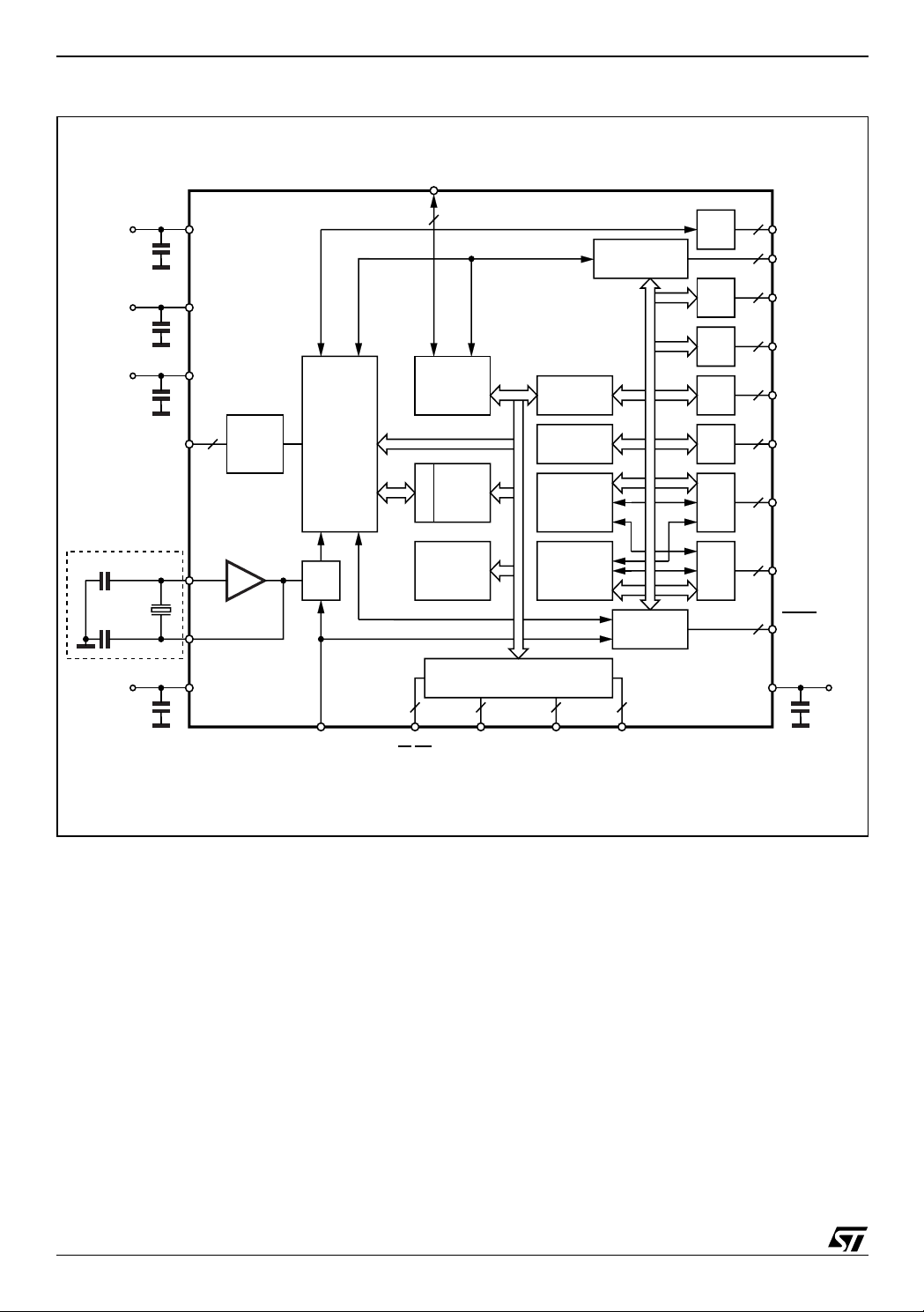
Figure 1. Block Diagram and Electrical Schematic
JTAG
V
DD
5
100nF
V
DDIO
100nF
V
DDIO
100nF
RF BUS
13
RADIO
I/F
BLUETOOTH
®
CORE
ARM7
TDMI
D
RAM
M
A
(*)
22pF
22pF
LPOCLKP
Y2
32KHz
LPO
BOOT
ROM
LPOCLKN
V
DD
100nF
VDDPLL
XIN
4
BOOT WAIT
RD/WR
EMI
3 20 16
CSN(0..2) ADDR(0..19) DATA(0..15)
(*) If a low-power clock is available, it can be connected to the LPOCLKP pin in stead of using a crystal
APB
BRIDGE
TIMER
START
DETECT
UART
FIFO
INTERRUPT
CONTROLLER
SYSTEM
CONTROL
PCM
USB
I2C
SPI
GPIO
UART
UART
4
2
2
2
4
16
8
2
2
D02TL550
PCM
EXT._INT1/2
USB
2
I
C
SPI
GPIO(O..15)
UART2
UART1
RESET
SYS_CLK_REQ
V
DD
100nF
4/20
4PINOUT
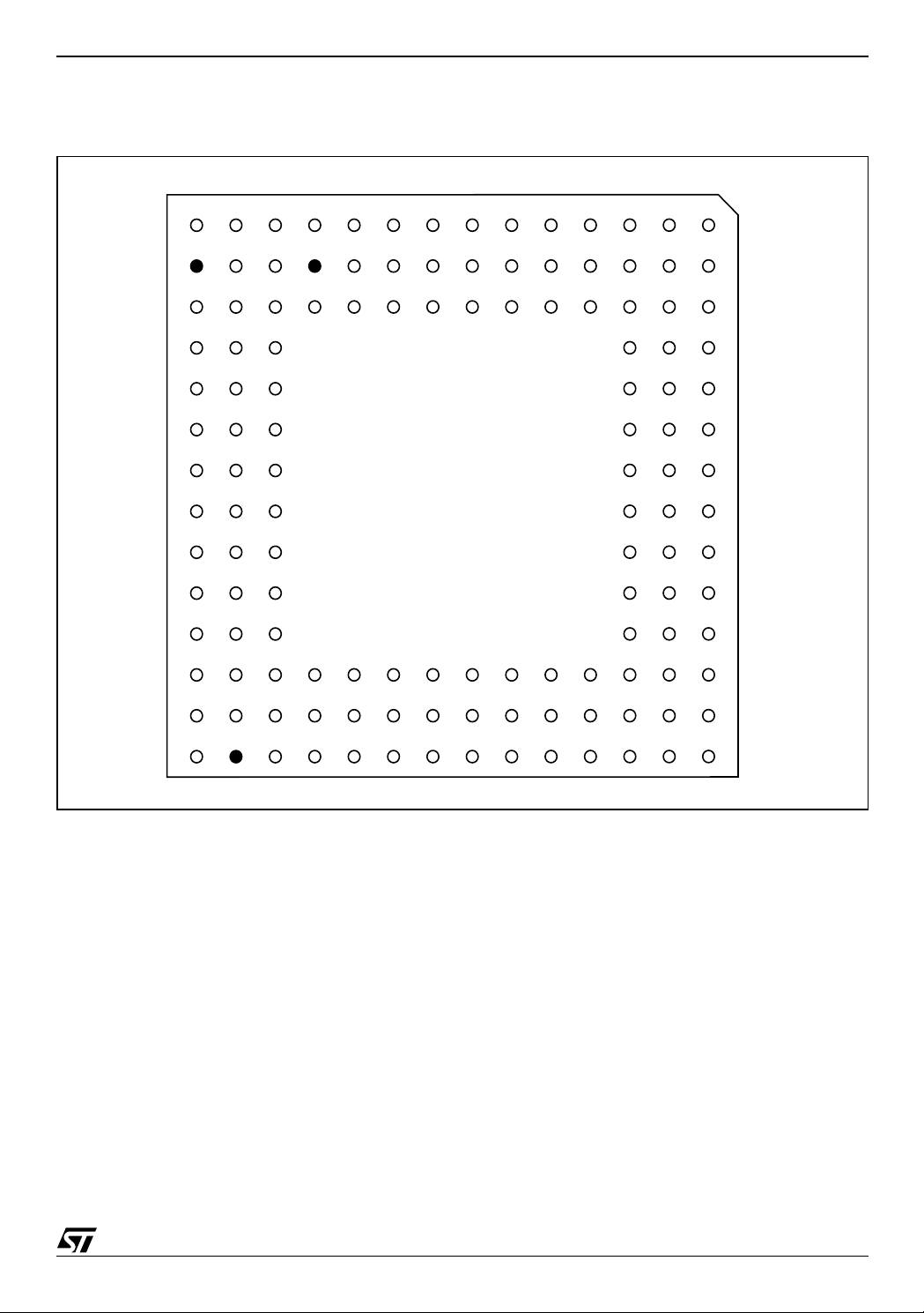
Figure 2. Pinout (Bottom view)
12
13
14
gpio9 gpio11 gpio14 vddio brxd bmosi bdclk bpaen brxen ant_sw tdi ntrst test xin
n.c. gpio10 gpio13 n.c. brclk bnden btxd vdd btxen vddio tdo tck nreset
gpio8 vddpll gpio12
vsspll gpio6 gpio7
gpio3 gpio4 gpio5
gpio0 gpio1 gpio2
lpo_
boot
clk_p
data
data
14
15
data13data12data
data10data
9
vss
vdd vdd vssiospi_frm vddio
data8 data7 data6 data0 addr17 vss
data5 data4 data2
data3 n.c. data1
gpio15 vssio bmiso bsen vss bpktctl vssio tms
lpo_
clk_n
wait
11
vss vss
8
9
10
11
addr13 addr10
addr19 addr16
addr18 addr15 addr14 addr11
vdd addr12 addr9 addr6 addr3 vss csn2 wrn
1
2
3
4
5
6
7
sys_
clk_req
uart1_
uart1_
rxd
i2c_clk int1 int2
vddio vssio
pcm_
clk
uart2_
rxd
uart2_
i2
uart2_
io1
addr5 addr2 vdd csn1
addr8 addr7 addr4 addr1 addr0 csn0 rdn
i2c_
txd
dat
pcm_
sync
pcm_a pcm_b
usb_
usb_
dn
dp
uart2_
uart2_
txd
i1
uart2_
uart2_
o1
o2
uart2_
vdd
io2
spi_
spi_
txd
clk
spi_
rxd
D02TL551
STLC2410B
A
B
C
D
E
F
G
H
J
K
L
M
N
P
4.1 Pin Description and Assignment
Table4 : STLC2410B pinlist shows the pinout of STLC2410B; there are 107 digital functional pins and 22
supply pins. The column "PU/PD" shows the pads implementing an internal weak pull-up/down, to fix value
if the pin is left open. This can not replace an external pull-up/down.
The pads are grouped according to two different power supply values, as shown in column "VDD":
– V1 for 3.3 V typical 2.7 - 3.6 V range
– V2 for 1.8 V typical 1.55 - 1.95 V range
Finally the column "DIR" describes the pin directions:
– I for inputs
– O for outputs
– I/O for input/outputs
– O/t for tristate outputs
5/20

STLC2410B
Table 8. Pin List
Name Pin # Description DIR PU/PD VDD PAD
Interface to external memory
int1 D2 External Interrupt used also as external wakeup I
int2 D1
boot G14
Second external interrupt
Select external boot from EMI or internal from ROM
I
I
wait H12 EMI external wait signal (left open) I PD
rdn P1 External read O
wrn N2 External write O
csn0 P2 External chip select bank 0 O
csn1 M3 External chip select bank 1 O
csn2 N3 External chip select bank 2 O
addr0 P3 External address bit 0 O
addr1 P4 External address bit 1 O
addr2 M5 External address bit 2 O
addr3 N5 External address bit 3 O
addr4 P5 External address bit 4 O
addr5 M6 External address bit 5 O
addr6 N6 External address bit 6 O
addr7 P6 External address bit 7 O
addr8 P7 External address bit 8 O
addr9 N7 External address bit 9 O
addr10 M7 External address bit 10 O
addr11 P8 External address bit 11 O
addr12 N8 External address bit 12 O
addr13 M8 External address bit 13 O
addr14 P9 External address bit 14 O
addr15 P10 External address bit 15 O
addr16 N10 External address bit 16 O
addr17 M10 External address bit 17 O
addr18 P11 External address bit 18 O
addr19 N11 External address bit 19 O
data0 M11 External data bit 0 I/O PD
data1 P12 External data bit 1 I/O PD
data2 N12 External data bit 2 I/O PD
data3 P14 External data bit 3 I/O PD
data4 N13 External data bit 4 I/O PD
data5 N14 External data bit 5 I/O PD
(1)
(1)
(1)
CMOS, 3.3V TTL
V1
schmitt trigger
V2 CMOS 1.8V
V2
slew rate control
CMOS 1.8V 4mA
V2
slew rate control
compatible
CMOS 1.8V
4mA
6/20

Table 8. Pin List (continued)
Name Pin # Description DIR PU/PD VDD PAD
data6 M12 External data bit 6 I/O PD
data7 M13 External data bit 7 I/O PD
data8 M14 External data bit 8 I/O PD
data9 K13 External data bit 9 I/O PD
data10 K14 External data bit 10 I/O PD
data11 J12 External data bit 11 I/O PD
data12 J13 External data bit 12 I/O PD
data13 J14 External data bit 13 I/O PD
data14 H14 External data bit 14 I/O PD
data15 H13 External data bit 15 I/O PD
SPI interface
spi_frm L3 Synchronous Serial Interface frame sync I/O
spi_clk M1 Synchronous Serial Interface clock I/O
spi_txd M2 Synchronous Serial Interface transmit data O/t
spi_rxd N1 Synchronous Serial Interface receive data I
(1)
UART interface
uart1_txd C2 Uart1 transmit data O/t
uart1_rxd C3 Uart1 receive data I
(2)
uart2_o1 J1 Uart2 modem output O
uart2_o2 J2 Uart2 modem output O/t
uart2_i1 H2 Uart2 modem input I
uart2_i2 H3 Uart2 modem input I
uart2_io1 J3 Uart2 modem input/output I/O
uart2_io2 K1 Uart2 modem input/output I/O
(2)
(2)
(2)
(2)
uart2_txd H1 Uart2 transmit data O/t
V2
slew rate control
CMOS, 3.3V TTL
compatible, 2mA
V1
slew rate control
schmitt trigger
CMOS, 3.3V TTL
V1
compatible, 2mA
slew rate control
CMOS, 3.3V TTL
V1
schmitt trigger
CMOS, 3.3V TTL
V1
compatible, 2mA
slew rate control
CMOS, 3.3V TTL
V1
schmitt trigger
CMOS, 3.3V TTL
V1
compatible, 2mA
slew rate control
CMOS, 3.3V TTL
V1
compatible, 2mA
slew rate control
V1
CMOS, 3.3V TTL
V1
V1 CMOS, 3.3V TTL
compatible, 2mA
tristate slew rate
V1
CMOS, 3.3V TTL
V1
compatible, 2mA
slew rate control
STLC2410B
CMOS 1.8V
4mA
tristate
compatible
compatible
compatible
control
7/20

STLC2410B
Table 8. Pin List (continued)
Name Pin # Description DIR PU/PD VDD PAD
uart2_rxd G3 Uart2 receive data I
I2C interface
i2c_dat C1 I2C data pin I/O
i2c_clk D3 I2C clock pin I/O
USB interface
usb_dn G1 USB - pin I/O
usb_dp G2 USB + pin I/O
GPIO interface
gpio0 F14 Gpio port 0 I/O PU
gpio1 F13 Gpio port 1 I/O PU
gpio2 F12 Gpio port 2 I/O PU
gpio3 E14 Gpio port 3 I/O PU
gpio4 E13 Gpio port 4 I/O PU
gpio5 E12 Gpio port 5 I/O PU
gpio6 D13 Gpio port 6 I/O PU
gpio7 D12 Gpio port 7 I/O PU
gpio8 C14 Gpio port 8 I/O PU
gpio9 A14 Gpio port 9 I/O PU
gpio10 B13 Gpio port 10 I/O PU
gpio11 A13 Gpio port 11 I/O PU
gpio12 C12 Gpio port 12 I/O PU
gpio13 B12 Gpio port 13 I/O PU
gpio14 A12 Gpio port 14 I/O PU
gpio15 C11 Gpio port 15 I/O PU
Clock and test pins
xin A1 System clock I
nreset B2 Reset I
sys_clk_req
B1 System clock request I/O
lpo_clk_p G13 Low power oscillator + / Slow clock input I
lpo_clk_n G12 Low power oscillator - O
test A2 Test mode I
(2)
(3)
(3)
(1)
(1)
(1)
PD
CMOS, 3.3V TTL
V1
V1 CMOS, 3.3V TTL
compatible, 2mA
V1
slew rate control
V1
V1
CMOS, 3.3V TTL
compatible, 4mA
V1
slew rate control
CMOS, 3.3V TTL
compatible, 4mA
V1
slew rate control
schmitt trigger
CMOS, 3.3V TTL
compatible, 4mA
V1
slew rate control
CMOS, 3.3V TTL
compatible, 2mA
V1
slew rate control
CMOS, 3.3V TTL
compatible, 2mA
V1
slew rate control
CMOS, 3.3V TTL
V1
schmitt trigger
CMOS, 3.3V TTL
compatible, 2mA
V1
slew rate control
V2
CMOS, 3.3V TTL
V1
compatible
tristate
tristate
tristate
tristate
tristate
tristate
compatible
tristate
compatible
8/20

Table 8. Pin List (continued)
Name Pin # Description DIR PU/PD VDD PAD
JTAG interface
ntrst A3 JTAG pin I
tck B3 JTAG pin I
tms C4 JTAG pin I
tdi A4 JTAG pin I
PD
(1)
PU
PU
tdo B4 JTAG pin (should be left open) O/t
PCM interface
pcm_a F2 PCM data I/O PD
pcm_b F1 PCM data I/O PD
pcm_sync E1 PCM 8kHz sync I/O PD
pcm_clk F3 PCM clock I/O PD
Radio interface
brclk B10 Transmit clock I
(1)
brxd A10 Receive data I
bmiso C9 RF serial interface input data I
(1)
bnden B9 RF serial interface control O
bmosi A9 RF serial interface output data O
bdclk A8 RF serial interface clock O
btxd B8 Transmit data O
bsen C8 Synthesizer ON O
bpaen A7 Open PLL O
brxen A6 Receive ON O
btxen B6 Transmit ON O
bpktctl C6 Packet ON O
ant_sw A5 Antenna switch O
CMOS, 3.3V TTL
V1
CMOS, 3.3V TTL
V1
CMOS, 3.3V TTL
V1
CMOS, 3.3V TTL
V1
compatible, 2mA
slew rate control
CMOS, 3.3V TTL
compatible, 2mA
V1
slew rate control
CMOS, 3.3V TTL
compatible, 2mA
V1
slew rate control
CMOS, 3.3V TTL
V1
CMOS, 3.3V TTL
V1
CMOS, 3.3V TTL
V1
compatible, 2mA
slew rate control
CMOS, 3.3V TTL
V1
compatible, 8mA
slew rate control
schmitt trigger
schmitt trigger
schmitt trigger
STLC2410B
compatible
compatible
compatible
tristate
tristate
compatible
compatible
(1) Should be strapped to vssio if not used
(2) Should be strapped to vddio if not used
(3) Should have a 10 kOhm pull-up if not used.
9/20

STLC2410B
Table 4. Pin List (continued)
Name Pin # Description
Power Supply
vsspll D14 PLL ground
vddpll C13 1.8V supply for PLL
vdd B7 1.8V Digital supply
vdd K2 1.8V Digital supply
vdd L12 1.8V Digital supply
vdd L14 1.8V Digital supply
vdd M4 1.8V Digital supply
vdd N9 1.8V Digital supply
vddio A11 3.3V I/O's supply
vddio B5 3.3V I/O's supply
vddio E3 3.3V I/O's supply
vddio L1 3.3V I/O's supply
vss C7 Digital ground
vss K3 Digital ground
vss K12 Digital ground
vss L13 Digital ground
vss M9 Digital ground
vss N4 Digital ground
vssio C5 I/O's ground vssio C10 I/O's ground vssio E2 I/O's ground vssio L2 I/O's ground
10/20

5 FUNCTIONAL DESCRIPTION
5.1 Baseband
STLC2410B
5.1.1 Overview
®
The baseband is fully compliant with the Bluetooth
specification 1.1, including:
– 7 slaves support.
– Asynchronous Connection-Less (ACL) link support giving data rates up to 721kb per second.
– Synchronous Connection-Oriented (SCO) link with support for 1 voice channel over the air interface.
– HW support for all packet types:
– ACL: DM1, 3, 5 and DH1, 3, 5.
– SCO: HV1, 2, 3, and DV1.
– Support for three PCM channels in the PCM interface.
– Architecture gives ultra-low power consumption.
– Ciphering support for up to 128-bit, configurable by software.
– Receiver Signal Strenght Indication (RSSI) support for power-controlled links.
– Flexible voice formats to Host and over air (CVSD, PCM 16/8-bit, A-law, µ-law).
– High quality filtering of voice packets enabling excellent audio quality.
– Point-to-multipoint support.
– Scatternet support, communication between two simultaneously running piconets.
®
– Full Bluetooth
software stack available.
– Low level link controller.
– Specific external power amplifier (PA) control for class1 support.
– Extended wake-up and interrupt functionality for HID support.
5.1.2 Processor and memory
– ARM7TDMI.
– 64Kbyte of static RAM.
– 4Kbyte of metal programmable ROM
– Extension of the ARM Bus to handle external program FLASH or RAM or dedicated peripherals.
– Data bus in byte or half word format (8-bit or 16-bit).
– Address bus 20-bit wide to support 1 Mbyte within each bank.
– Direct Support for 3 external devices.
– Access to slow peripherals.
11/20

STLC2410B
6 GENERAL SPECIFICATION
6.1 SYSTEM CLOCK
The STLC2410B works with a single clock provided on the XIN pin. The value of this external clock should
be 13MHz ±20ppm (overall).
6.1.1 SLOW CLOCK
The slow clock is used by the baseband as reference clock during the low power modes. Compared to the
13MHz clock, the slow clock only requires an accuracy of ±250ppm (overall).
Several options are foreseen in order to adjust the STLC2410B behaviour according to the features of the
radio used:
– if the system clock (e.g. 13MHz) is not provided at all times (power consumption saving) and no slow
clock is provided by the system, a 32 kHz crystal must be used by the STLC2410B (default mode).
– if the system clock (e.g. 13MHz) is not provided at all times (power consumption saving) and the system
provides a slow clock at 32kHz or 3.2kHz, this signal in simply connected to the STLC2410B
(lpo_clk_p).
– if the system clock (e.g. 13MHz) is provided at all times, the STLC2410B generates from the 13MHz
reference clock an internal 32kHz clock. This mode is not an optimized mode for power consumption.
6.2 BOOT PROCEDURE
The boot code instructions are the first that ARM7TDMI executes after an HW reset. All the internal device's registers are set to their default value.
There are 2 types of boot:
– external flash boot.
When boot pin is set to `1` (connected to VDD), the STLC2410B boots on its external memory which is
normally a flash memory.
– UART download boot from ROM.
When boot pin is set to `0` (connected to GND), the STLC2410B boots on its internal ROM (needed to
download the new firmware).
When booting on the internal ROM, the STLC2410B will monitor the UART interface for approximately 1.4
second. If there is no request for code downloading during this period, the ROM jumps to external flash.
6.3 CLOCK DETECTION
The STLC2410B has a automatic slow clock frequency detection (32kHz, 3.2kHz or none).
6.4 MASTER RESET
When the device's reset is held active (NRESET is low), all two uart txd pins (UART1_TXD and
UART2_TXD) are driven low. When the NRESET returns high, the device starts to boot.
Remark: The device should be held in active reset for minimum 20ms in order to guarantee a complete
reset of the device.
6.5 INTERRUPTS/WAKE-UP
The external pins int1 and int2, and up to 8 GPIOs can be used both as external interrupt source and as
wake-up source. In addition the chip can be woken-up by USB or Uart Rx.
12/20

STLC2410B
7 INTERFACES
7.1 UART Interface
The chip contains two enhanced (128-byte FIFO depth, sleep mode, 127 Rx and 128 Tx interrupt tresholds) UARTs named UART1 and UART2 compatible with the standard M16550 UART.
For UART1, only Rx and Tx signals are available (mainly used for debug purposes and in test mode).
UART2 features:
– standard HCI UART transport layer:
– all HCI commands as described in the Bluetooth
– ST specific HCI command (check STLC2410B Software Interface document for more information)
– RXD, TXD, CTS, RTS on permanent external pins
– 128-byte FIFOs, for transmit and for receive
– Default configuration: 57.6 kbits/s
– Specific HCI command to change to the following baud rates:
Table 9. List of supported baud rates
Baud rate
– 57.6 k (default) 4800
921.6k 38.4 k 2400
460.8 k 28.8 k 1800
230.4 k 19.2 k 1200
153.6 k 14.4 k 900
115.2 k 9600 600
76.8 k 7200 300
®
specification 1.1
7.2 Synchronous Serial Interface
The Synchronous Serial Interface is a flexible module that supports full-duplex and half-duplex synchronous communications with external devices in Master and Slave mode. It allows the STLC2410B to communicate with peripheral devices.
The Synchronous Serial Interface is also capable of inter processor communications in a multiple-master
system. This interface is flexible enough to interface directly with numerous standard product peripherals.
This Synchronous Serial Interface peripheral features:
– full duplex, four-wire synchronous transfers.
– Microwire half duplex transfer using 8-bit control message
– programmable clock polarity and phase.
– transmit data pin tri state able when not transmitting
– Master or Slave operation
– Programmable clock bit rate up to XIN/4
– Programmable data frame from 4 bits to 16 bits.
– Independent transmit and receive 16 words FIFO.
– Internal loopback
7.3 I2C Interface
The I2C port is used both to connect to an external E2PROM and to access I2C peripherals like the
STw5094 Codec. The I2C implemented in the STLC2410B is a master I2C, it has the full control of the
I2C bus at all time. I2C slave functionality is not supported, so any other I2C attached to the I2C bus must
be slave, otherwise bus contention will occur.
13/20

STLC2410B
Figure 3. I2C BUS master flow diagram
IDLE
STA
SEND START
SEND ADDR
STA
RECEIVE
ACKNOWLEDGE
RX
RECEIVE DATA
SEND
ACKNOWLEDGE
RX TXSTP STP
STA STA
SEND STOP
TX
SEND DATA
ACKNOWLEDGE
TX DATARX DATA
RECEIVE
D02TL554
7.4 USB Interface
The USB interface is compliant with the USB 2.0 full speed specification. Max throughput on the USB interface is 12 Mbit/s.
Figure 4 gives an overview of the main components needed for supporting the USB interface, as specified
in the Bluetooth
®
Core Specification ( Part H:2). For clarity, the serial interface (including the UART Trans-
port Layer) is also shown.
14/20

Figure 4. USB Interface
STLC2410B
HCI
USB TRANSPORT LAYER UART TRANSPORT LAYER
USB
DEVICE
REGISTERS
FIFOs
USB DRIVER SERIAL DRIVER
IRQ
IRQ
RTOS
UART
DEVICE
REGISTERS
FIFOs
STLC2410B HW
D02TL555
The USB device registers and FIFOs are memory mapped. The USB Driver will use these registers to access the USB interface. The equivalent exists for the HCI communication over UART.
For transmission to the host, the USB & Serial Drivers interface with the HW via a set of registers and
FIFOs, while in the other direction, the hardware may trigger the Drivers through a set of interrupts (identified by the RTOS, and directed to the appropriate Driver routines).
7.5 JTAG Interface
The JTAG interface is compliant with the JTAG IEEE Std 1149.1. Its allows both the boundary scan of the
digital pins and the debug of the ARM7TDMI application when connected with the standard ARM7 development tools.
7.6 RF Interface
The STLC2410B radio interface is compatible to BlueRF (unidirectional RxMode2 for data and unidirectional serial interface for control).
7.7 PCM voice interface
The voice interface is a direct PCM interface to connect to a standard CODEC (e.g. STw5093 or
STw5094) including internal decimator and interpolator filters. The data can be linear PCM (13-16bit), µLaw (8bit) or A-Law (8bit). By default the codec interface is configured as master. The encoding on the air
interface is programmable to be CVSD, A-Law or µ-Law.
The PCM block is able to manage the PCM bus with up to 3 timeslots.
PCM clock and data are in master mode available at 2 MHz or at 2.048 MHz to allow interfacing of standard codecs.
15/20

STLC2410B
The four signals of the PCM interface are:
– PCM_CLK : PCM clock
– PCM_SYNC : PCM 8kHz sync
– PCM_A : PCM data
– PCM_B : PCM data
Directions of PCM_A and PCM_B are software configurable.
Figure 5. PCM (A-law, µ-law) standard mode
PCM_CLK
PCM_SYNC
PCM_A B B
PCM_B
0 1 2 3 4 5 6 7 8 9 10 11 12 13 14 15
B
125µs
Figure 6. Linear mode
PCM_CLK
PCM_SYNC
PCM_A
PCM_B
0 1 2 3 4 5 6 7 8 9 10 11 12 13 14 15
125µs
Table 10. PCM interface timing.
Symbol Description Min Typ Max Unit
PCM Interface
F
pcm_clk
F
pcm_sync
t
WCH
t
WCL
t
WSH
t
SSC
t
SDC
t
HCD
t
DCD
Frequency of PCM_CLK (master) - 2048 kHz
Frequency of PCM_SYNC 8 kHz
High period of PCM_CLK 200 ns
Low period of PCM_CLK 200 ns
High period of PCM_SYNC 200 ns
Setup time, PCM_SYNC high to PCM_CLK low 100 ns
Setup time, PCM_A/B input valid to PCM_CLK low 100 ns
Hold time, PCM_CLK low to PCM_A/B input invalid 100 ns
Delay time, PCM_CLK high to PCM_A/B output valid 150 ns
B
D02TL558
D02TL559
16/20

Figure 7. PCM interface timing
6
PCM_CLK
t
WCH
t
WCL
t
STLC2410B
SSC
PCM_SYNC
PCM_A/B in
PCM_B/A out
t
WSH
MSB MSB-1 MSB-2 MSB-3 MSB-4
t
SDC
t
DCD
MSB MSB-1 MSB-2 MSB-3 MSB-4
t
HCD
D02TL557
8 HCI UART TRANSPORT LAYER
The UART Transport Layer is specified by the Bluetooth
®
SIG ( Part H:4), and allows HCI level commu-
nication between a host controller (STLC2410B) and a host (e.g. PC), via a RS232 interface.
The objective of this HCI UART Transport Layer is to make it possible to use the Bluetooth
®
HCI over a
serial interface between two UARTs on the same PCB. The HCI UART Transport Layer assumes that the
UART communication is free from line errors.
8.1 UART Settings
The HCI UART Transport Layer uses the following settings:
– Baud rate: Configurable (Default baud rate: 57.6 kbits/s)
– Number of data bits: 8
– Parity bit: no parity
– Stop bit: 1 stop bit
– Flow control: RTS/CTS
– Flow-off response time: 3 ms
Flow control with RTS/CTS is used to prevent temporary UART buffer overrun. It should not be used for
flow control of HCI, since HCI has its own flow control mechanisms for HCI commands, HCI events and
HCI data.
If CTS is 1, then the Host/Host Controller is allowed to send.
If CTS is 0, then the Host/Host Controller is not allowed to send.
The flow-off response time defines the maximum time from setting RTS to 0 until the byte flow actually
stops. The signals should be connected in a null-modem fashion; i.e. the local TXD should be connected
to the remote RXD and the local RTS should be connected to the remote CTS and vice versa.
Figure 8. UART Transport Layer
BLUETHOOTH
HOST
BLUETHOOTH HCI
HCI UART TRANSPORT LAYER
BLUETHOOTH
HOST
CONTROLLER
D02TL55
17/20

STLC2410B
9 HCI USB TRANSPORT LAYER
The USB Transport Layer has been specified by the Bluetooth
®
SIG (Part H:2), and allows HCI level communication between a host controller (STLC2410B) and a host (e.g. PC), via a USB interface. The USB
Transport Layer is completely implemented in SW. It accepts HCI messages from the HCI Layer, prepares
it for transmission over a USB bus, and sends it to the USB Driver. It reassembles the HCI messages from
USB data received from the USB Driver, and sends these messages to the HCI Layer. The Transport Layer does not interprete the contents (payload) of the HCI messages; it only examines the header.
10 POWER CLASS1 SUPPORT
The chip can control an external power amplifier (PA). Several signals are duplicated on GPIOs for this
purpose in order to avoid digital/analog noise loops in the radio.
The Class1_En register enables the alternate functions of GPIO[15:6] to generate the signals for driving
an external PA in a Bluetooth
®
power class1 application.
Every bit enables a dedicated signal on a GPIO pin, as described in Table 11 : Power Class 1 functionality.
Table 11. Power Class 1 functionality
Class1_En bit involved GPIO description (when class1_En bit = ‘1’)
rxon gpio[6] outputs a copy of rx_on pin to switch LNA/RF switch on/off
not rxon gpio[7] outputs an inverted copy of rx_on pin to switch LNA/RF switch on/off
PA0 gpio[8] Bit 0 of the PA value for the current connection
PA1 gpio[9] Bit 1 of the PA value for the current connection
PA2 gpio[10] Bit 2 of the PA value for the current connection
PA3 gpio[11] Bit 3 of the PA value for the current connection
PA4 gpio[12] Bit 4 of the PA value for the current connection
PA5 gpio[13] Bit 5 of the PA value for the current connection
PA6 gpio[14] Bit 6 of the PA value for the current connection
PA7 gpio[15] Bit 7 of the PA value for the current connection
rx_on is the same as the rx_on output pin. Not rx_on is the inverted signal, in order to save components
on the application board.
PA7 to PA0 are the power amplifier control lines. They are managed, on a connection basis, by the baseband core. The Power Level programmed for a certain Bluetooth
as specified in the Bluetooth
®
SIG spec.
®
connection is manged by the firmware,
18/20

STLC2410B
mm inch
DIM.
MIN. TYP. MAX. MIN. TYP. MAX.
A 1.010 1.200 0.040 0.047
A1 0.150 0.006
A2 0.820 0.032
b 0.250 0.300 0.350 0.010 0.012 0.014
D 7.850 8.000 8.150 0.310 0.315 0.321
D1 6.500 0.256
E 7.850 8.000 8.150 0.310 0.315 0.321
E1 6.500 0.256
e 0.450 0.500 0.550 0.018 0.020 0.022
f 0.600 0.750 0.900 0.024 0.029 0.035
ddd 0.080 0.003
OUTLINE AND
MECHANICAL DATA
Body:
8 x 8 x 1.20mm
TFBGA132
Fine Pitch Ball Grid Array
7146828 A
19/20

STLC2410B
Information furnished is believed to be accurate and reliable. However, STMicroelectronics assumes no responsibility for the consequences
of use of such information nor for any infringement of patents or other rights of third parties which may result from its use. No license is granted
by implication or otherwise un der any patent or patent rights of STMicroelectronics. Specifications mentioned in this publication are subject
to change without notice. This publication supersedes and replaces all information previously supplied. STMicroelectronics products are not
authorized for use as critical components in life support devices or systems without express written approval of STMicroelectronics.
The ST logo is a registered trademark of STMicroelectronics.
The BLUETOOTH® word mark and logos are owned by the Bluetooth SIG, Inc. and any use of such marks by STMicroelectroni cs is under license.
All other names are the property of their respective owne rs
© 2004 STMicroelectronics - All rights reserved
STMicroelectronics GROUP OF COMPANIES
Australia - Belgium - Brazil - Canada - China - Czech Republic - Finland - France - Germany - Hong Kong - India - Israel - Italy - Japan -
Malaysia - Malta - Morocco - Singapore - Spain - Sweden - Switzerland - United Kingdom - United States
www.st.com
20/20
 Loading...