

Page 1
Any and all SANYO products described or contained herein do not have specifications that can handle
applications that require extremely high levels of reliability, such as life-support systems, aircraft’s
control systems, or other applications whose failure can be reasonably expected to result in serious
physical and/or material damage. Consult with your SANYO representative nearest you before using
any SANYO products described or contained herein in such applications.
SANYO assumes no responsibility for equipment failures that result from using products at values that
exceed, even momentarily, rated values (such as maximum ratings, operating condition ranges,or other
parameters) listed in products specifications of any and all SANYO products described or contained
herein.
Thick Film Hybrid IC
5V/5A Single Output Separate Excitation
Chopper Regulator
Ordering number:EN*6107
STK740-470
SANYO Electric Co.,Ltd. Semiconductor Company
TOKYO OFFICE Tokyo Bldg., 1-10, 1 Chome, Ueno, Taito-ku, TOKYO, 110-8534 JAPAN
Preliminary
Overview
The STK740-470 is a separate-excitation step-down
chopper regulator hybrid IC for the secondstage circuit.
This IC incorporates in the package all the necessary
circuits for a chopper regulator including power switch,
error amplifier, soft start, shutdown type output short
protection, low-voltage malfunction prevention, on/off,
and snubber circuits. Therefore, external components
required are input and output capacitors and a choke coil
only and this allows this IC to be used to construct a
large-current (5A) chopper regulator as if a 3-pin regulator were used. DC8V to 18V input voltage can be
handled and up to 5A of output current is supported.
Applications
• Local power supply for the equipment of which input
rating is DC9V to 15V.
Features
• Adoption of Sanyo IMST ; Insulated Metal Substrate
Technology, allows the circuit to be operated without
using a heat sink (see “No Fin Output Current Derating” chart in the page 6).
• Typical efficiency of 90% at DC 12V input, 2.5A
output.
• Fine adjustment of output voltage enable.
• 50 kHz operating frequency.
• Low-RON resistance power MOSFET adopted.
• Low-VF Schottky barrier diode adopted.
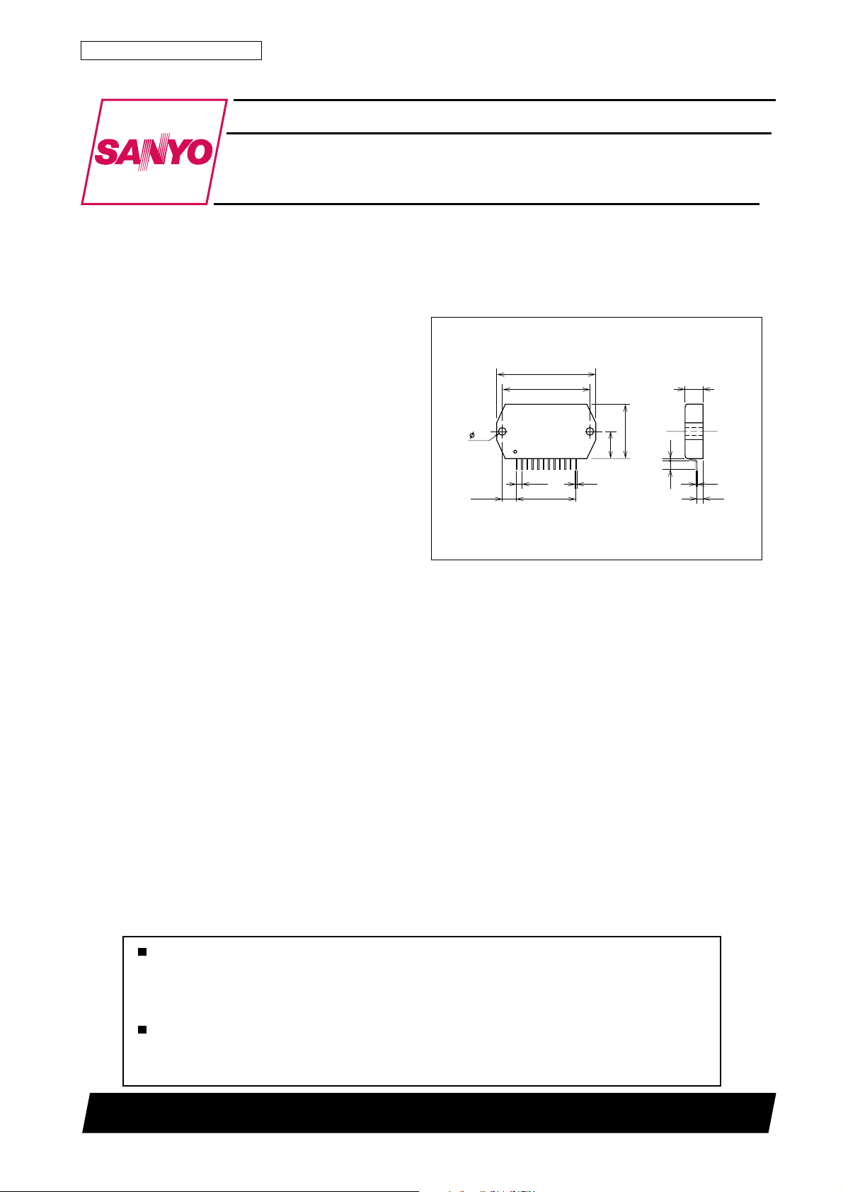
Package Dimensions
unit:mm
4170-SIP28
[STK740-470]
46.6
41.2
3.6
1
2.54
(6.63)
11×2.54=27.94
12
0.5
12.7
25.5
8.5
1.0
0.4
4.0
2.9
SANYO : SIP-28
63099RM (KT) No.6107–1/10
Page 2
STK740-470
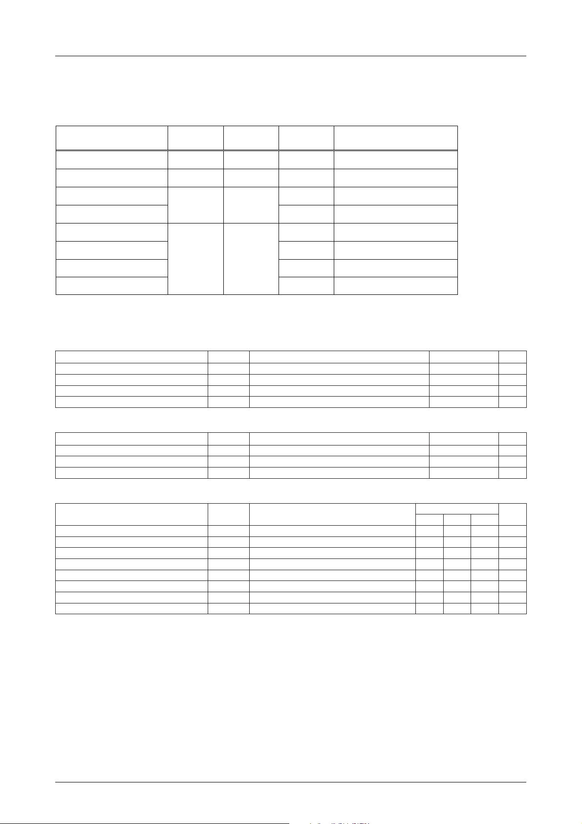
Series Construction
This product is listed in a product series due to its property such as output voltage, output current, package, and other
similar items. Since some prducts listed in the table below is under development, please refer to your Sanyo sales
representative for details.
Type number Input voltage
STK740-411
∗
STK740-420
∗
STK740-441
STK740-450
STK740-471
STK740-470
STK740-480
STK740-490
4 to 8V
4 to 8V
4 to 8V
8 to 18V
Output voltage Output current
2.5V
2.5V
5A
10A
5A
3.3V
10A
5A
5A
5.0V
10A
15A
25.5 × 46.6 × 8.5mm,12pins
25.5 × 46.6 × 8.5mm,12pins
25.5 × 46.6 × 8.5mm,12pins
25.5 × 46.6 × 8.5mm,12pins
25.5 × 46.6 × 8.5mm,12pins
* : Under planning
Specifications
Maximum Ratings at Ta = 25˚C, Tc = 25˚C, unless otherwise specified.
retemaraPlobmySsnoitidnoCsgnitaRtinU
erutarepmetetartsbusCIgnitarepOxamcT 501+
erutarepmetgnitarepOrpoT 58+ot01–
erutarepmetegarotSgtsT 511+ot03–
egatlovtupniCDV
xam21dna,11,6sniP 02V
NI
Package dimensions
(output pins not included)
26 × 37 × 4.5mm,12pins
26 × 37 × 4.5mm,12pins
26 × 37 × 4.5mm,12pins
˚C
˚C
˚C
Recommended Operating Conditions at Ta = 25˚C
retemaraPlobmySsnoitidnoCsgnitaRtinU
erutarepmetetartsbusCIgnitarepOcT 58+ot0
egatlovtupniCDV
tnerrucdaoLoItiucricdednemmocerehtnI 5ot1A
NI
tiucricdednemmocerehtnI 61ot8V
˚C
Electrical Characteristics at Tc = 25˚C, in the specified circuit, VIN = 12V, IO = 1A, unless othrwise specified
retemaraPlobmySsnoitidnoC
egatlovtuptuOoV9.40.51.5V
noitalugereniL
noitalugerdaoL
ycneiciffE
ycneuqerfgnitarepOcsof540555zHk
tnerrucffotuCI
tiucricffo/nOffoVnip1–22.023.0V
tneiciffeocerutarepmetegatlovtuptuOT
∆ LV
∆ OV
η
TUC
OVC
V
NI
Tc=+25 to +85˚C
V61otV8=–001–Vm
A5otA1=oI–001–Vm
A5.2=oI–09–%
edomhctal,nip6–6.1–Am
nimpytxam
sgnitaR
–7.1±–
mV/˚C
tinU
No.6107–2/10
Page 3
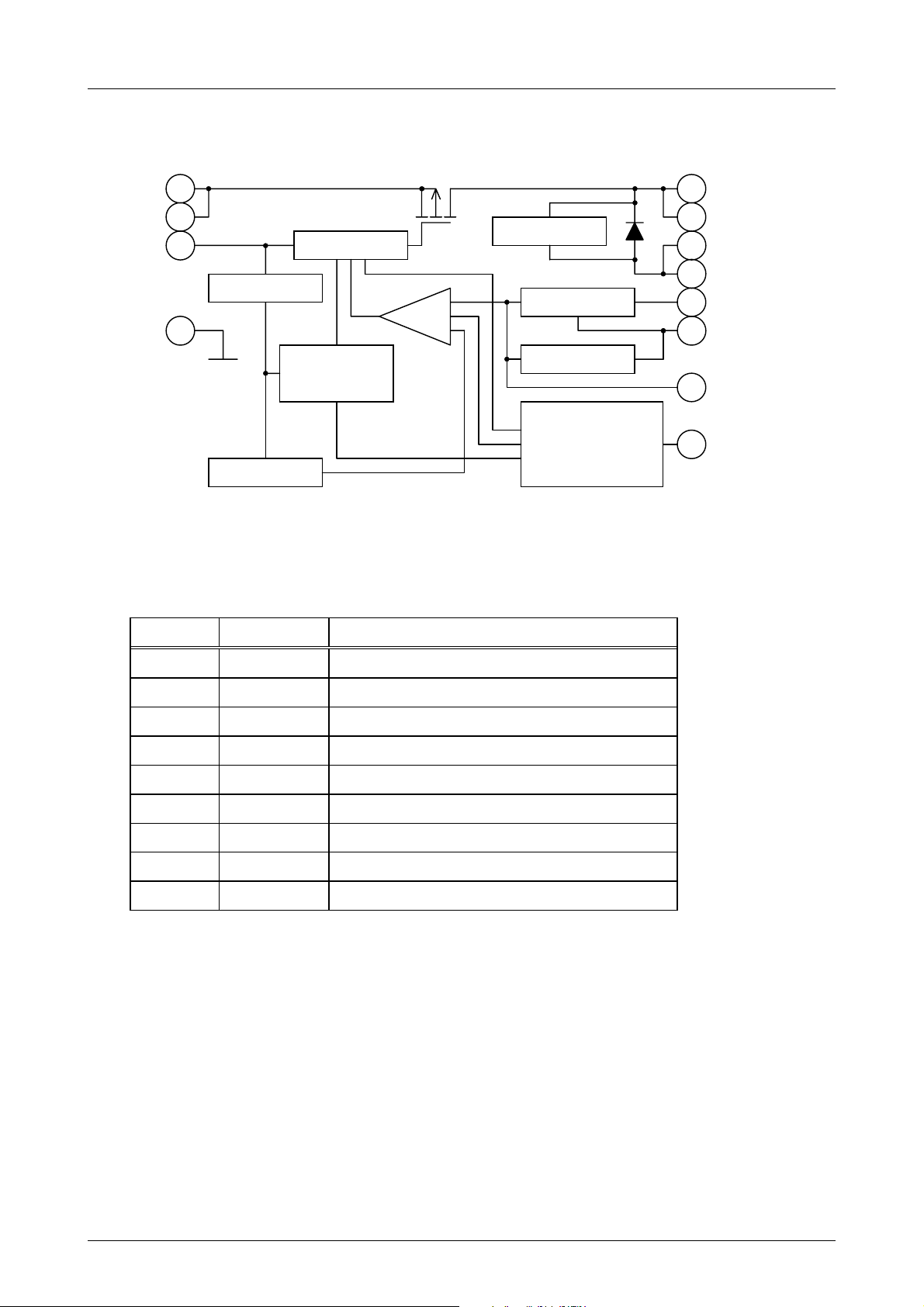
Block Diagram
STK740-470
12
V
IN
11
CC
6
5
V
GND
Pin Descriptions
Reference voltage
SUB
Oscillator
Drive circuit
Low-voltage
malfunction
prevention circuit
TR1
PWM
Snubber circuit
Error amplifier
Phase
compensation
On/off circuit
Soft start circuit
Short protection circuit
D1
10
9
8
7
2
3
4
1
OUT
A
V
S
V
ADJ
F
B
ON/OFF
Number Pin name
1 ON/OFF
V
V
V
S
ADJ
F
B
CC
IN
2
3
4
5 GND
6
7,8 A
9,10 OUT
11,12 V
Description
Remoteon/offswitching
Outputvoltagesensing
Outputvoltagefineadjustment
Feedback(erroramplifieroutput),phasecompensation
Ground
Powersupplyforcontrolblock
Flywheeldiodeanode
Output
Inputsupplyvoltage
No.6107–3/10
Page 4
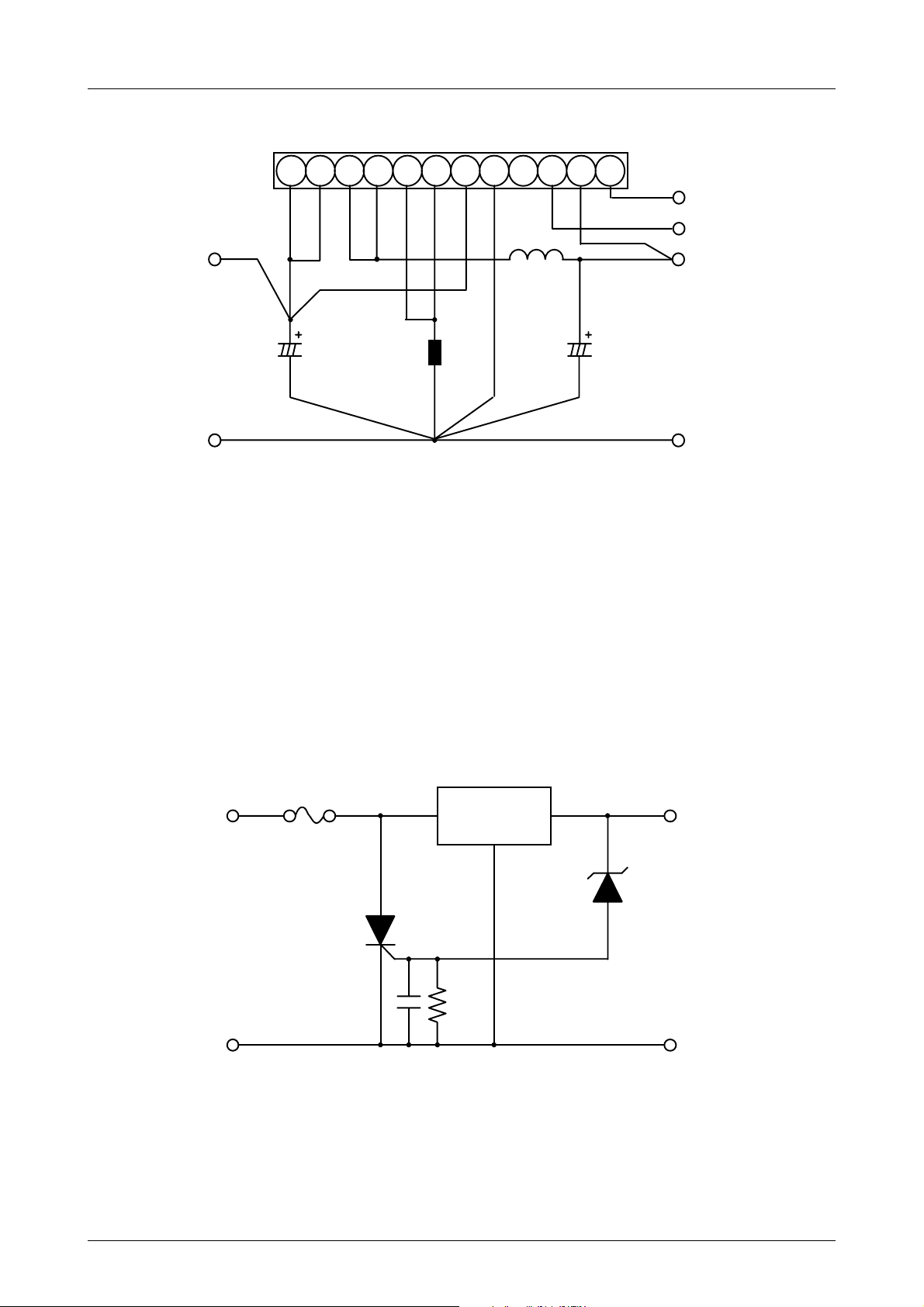
Test Circuit
STK740-470
1112
DC
INPUT
C1 C2FB
GND
C1 : 47µF/25V (OS capacitor)
C2 : 1000µF/16V×2
L1 : 30µH
FB : Ferrite-bead core
10
9
8
567
234
1
ON/OFF
Vo adjust
OUTPUT
L1
(5V)
GND
Overvoltage Protection Circuit
In a constant-voltage power supply circuit output voltage may generally exceed the stipulated rating (equivalent to input
voltage) when the circuit is broken down or the IC and the printed circuit board is wrongly soldered. Therefore ov erv oltage
protection circuit is recommended to use to minimize the damages caused by the overvoltage.
Sample the overvoltage protection circuit
FUSE
DC
Regulator
OUTPUT
INPUT
SCR
GND
CR
GND
No.6107–4/10
Page 5
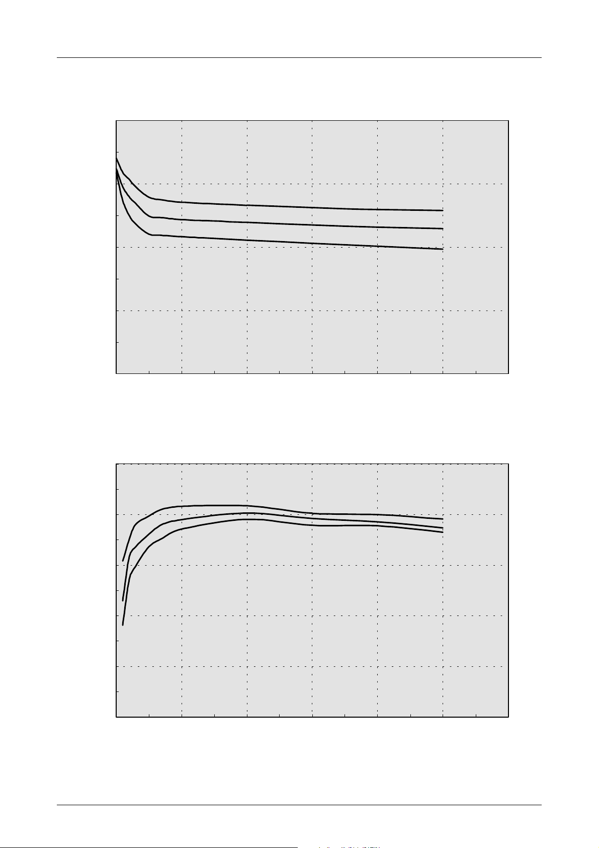
STK740-470
Sample Characteristics at Ta = 25˚C, in the test circuit
Output Voltage vs.Output Current
5.4
5.2
VIN=15V
=12V
V
IN
5.0
=9V
V
IN
Output Voltage Vo[V]
4.8
4.6
0123456
Output Current Io[A]
Efficiency vs.Output Current
100
90
VIN=9V
=12V
V
IN
=15V
V
IN
80
70
Efficiency η[%]
60
50
01 234 56
Output Current Io[A]
No.6107–5/10
Page 6
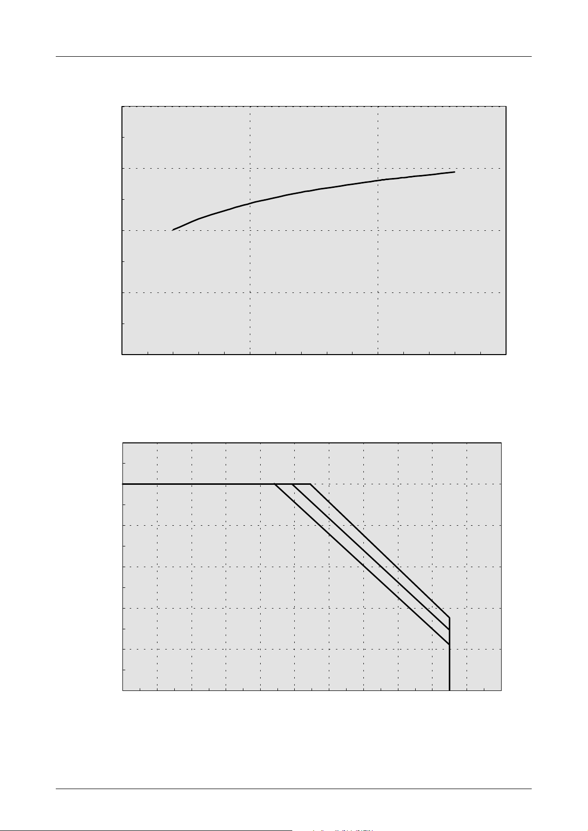
5.4
5.2
5.0
Output Voltage Vo[V]
4.8
STK740-470
Output Voltage vs.Input Voltage
Io=5A
4.6
5101520
6.0
5.0
4.0
3.0
2.0
Output Current Io[A]
Input Voltage V
No Fin Output Current Derating
IN
[V]
VIN=9V
=12V
V
IN
1.0
V
0.0
-10 0 10 20 30 40 50 60 70 80 90 100
Ambient Temperature Ta[°C]
IN
=15V
No.6107–6/10
Page 7
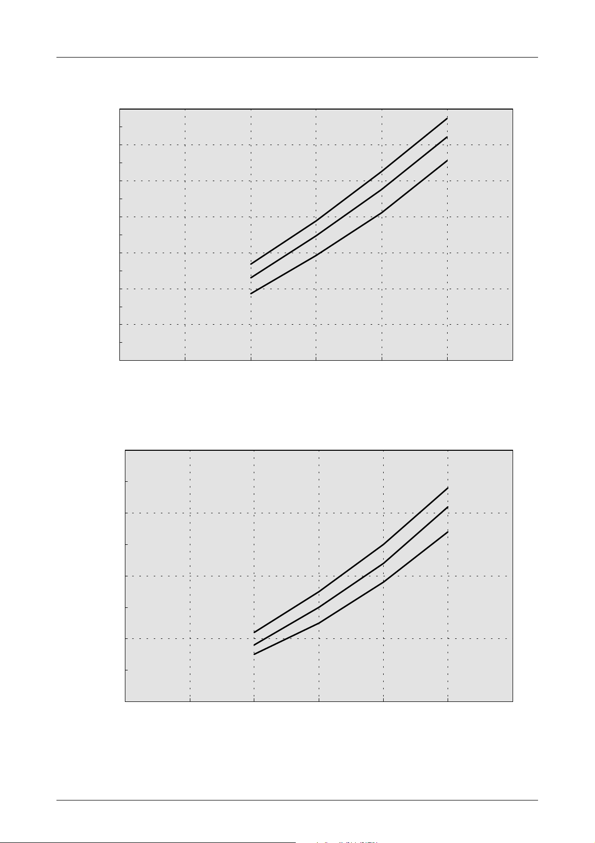
STK740-470
No Fin ∆Tc vs.Output Current
70
V
=15V
IN
=12V
V
IN
60
V
=9V
IN
50
40
Tc[deg.]
30
∆
20
10
0
0123456
Output Current Io[A]
4.0
3.0
[W]
D
2.0
Power Dissipation P
1.0
0.0
0213456
Power Dissipation vs Output Current
Output Current Io[A]
V
V
V
=15V
IN
=12V
IN
=9V
IN
No.6107–7/10
Page 8
STK740-470
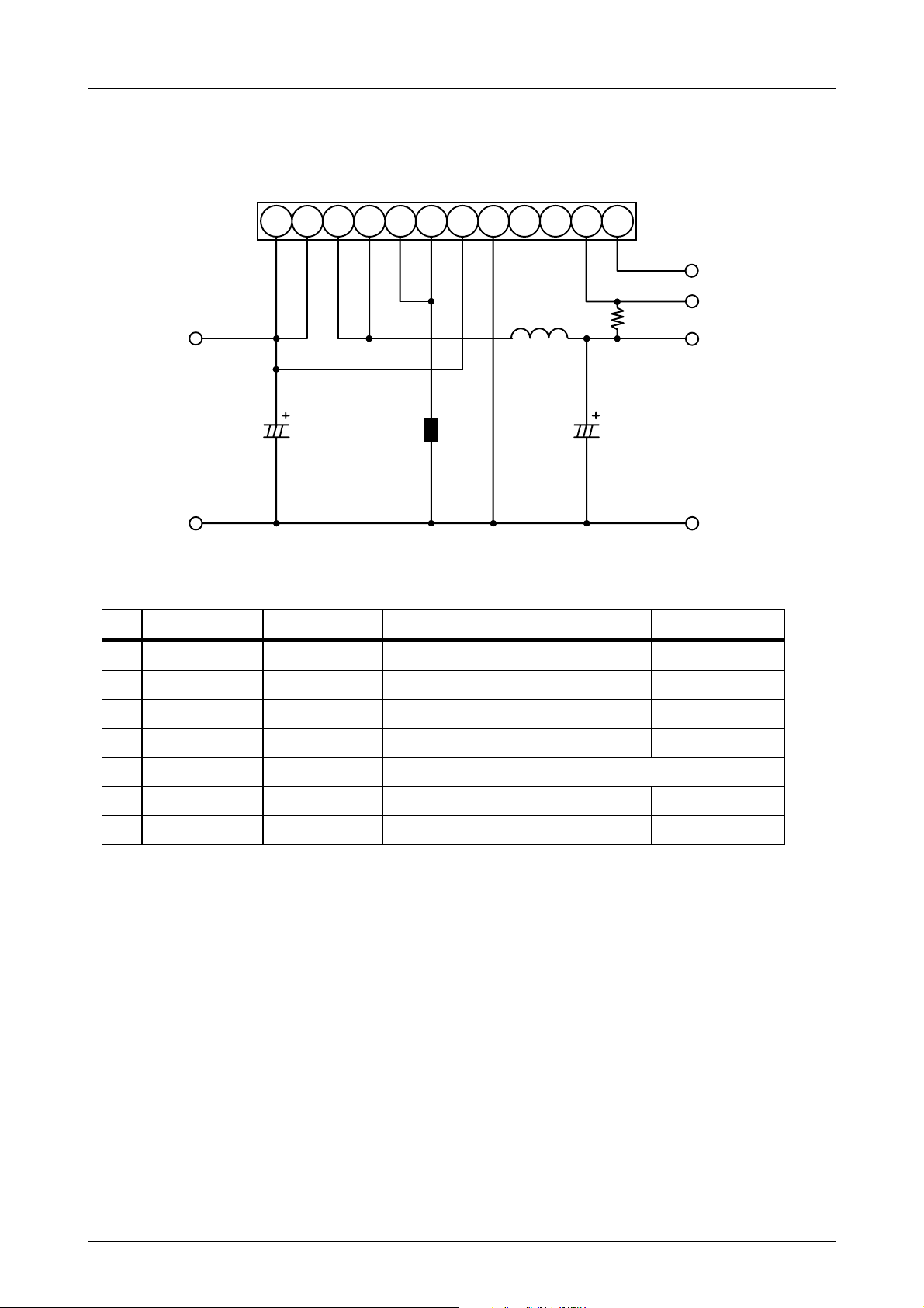
Eveluation Board
The evaluation board is provided to evaluate this hybrid IC
♦ Equivalent Circuit
V
N
I
GND
♦ Parts Table
Electrolytic capacitor
C1
12
11
10
56789
4
23
1
IC1
ON/OFF
Vs
R2
Vo
L1
C1 FB1
C2
GND
Part name Requirements Number Manufacturer Notes
47µF/25V
1
Sanyo Electronic component co., ltd.
OS capacitor
Electrolytic capacitor 2 Sanyo Electronic component co., ltd. Low impedance (CG)
C2
Resistor
R2
Jumper 1
R3
Jumper 1 Use a fuse resistor (20 to 30Ω) when needed
R6
Ferrite-bead core BL02RN1-R62 1 Murata manufacturing co., ltd.
FB1
Choke coil HK-10S100-4500 1 Toho zinc co., ltd. 45µH, 5A
L1
1000µF/16V
100Ω
1
♦ Notes on pattern designing
1 Place VCC pin (pin 6) and VIN pins (pin 11 and 12) lines separately and use an input capacitor (+) for connection.
2 Place GND pin (pin 5) and A pin (pins 7 and 8) lines separately.
3 Connect A pin (pins 7 and 8) with the input capacitor (–) through a Ferrite-bead core.
4 Connect GND pin (pin 5) with the input capacitor (–) or the output capacitor (–). However, connect with the
output capacitor (–) unless otherwise specified.
5 Shorten the length of the line between the input capacitor (–) and the output capacitor (–) as well as possible.
6 Connect VS pin (pin 2) with the output capacitor (+).
No.6107–8/10
Page 9
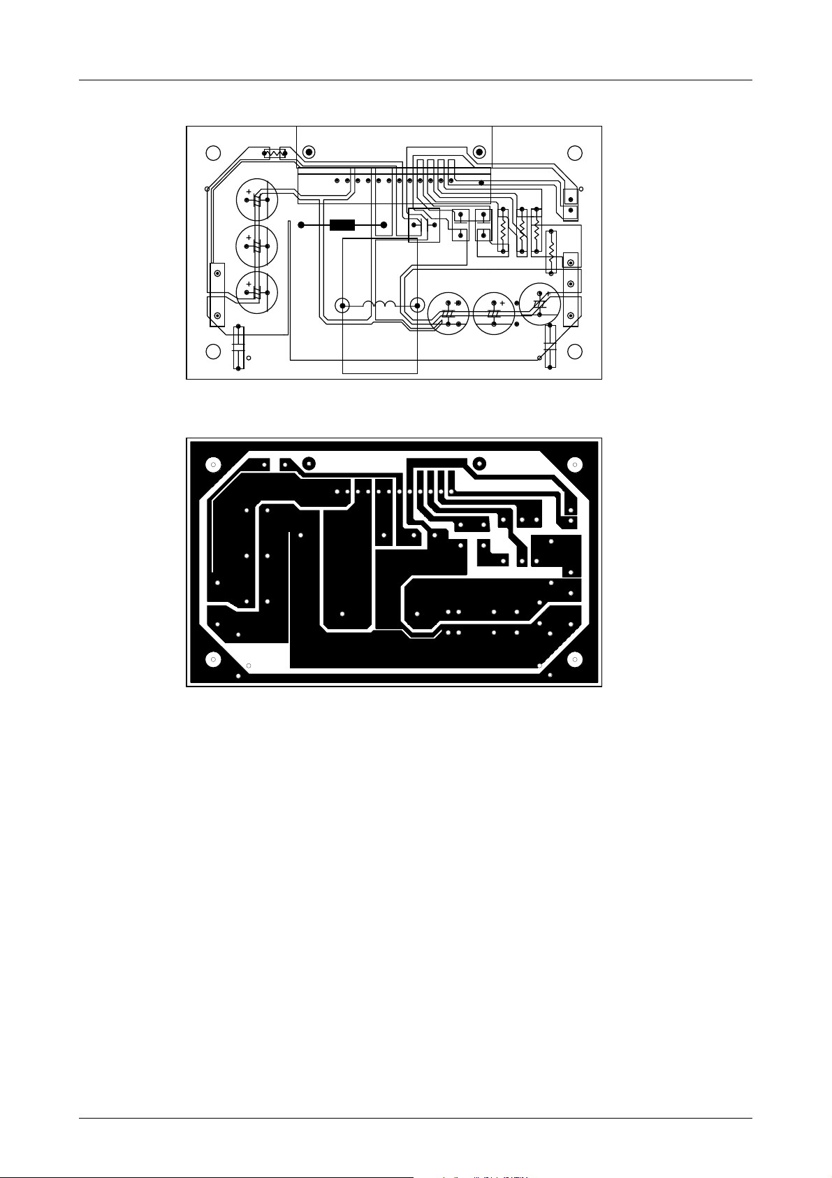
♦ Perspective Wiring Layout (from soldered side)
R6
C1a
IC1
FB1
STK740-470
R5
R1R2
R3
CN3
S-GND
ON/OFF
C1b
VIN
GND
CN1
C1c
C8
♦ Circuit Pattern (soldered side)
STK740-400 TEST-B
L1
C4 C5 C6
C2a
C2b
C2c
C9
+Vs
+Vo
GND
CN2
No.6107–9/10
Page 10
STK740-470
Specifications of any and all SANYO products described or contained herein stipulate the performance,
characteristics, and functions of the described products in the independent state, and are not guarantees
of the performance, characteristics, and functions of the described products as mounted in the customer's
products or equipment. To verify symptoms and states that cannot be evaluated in an independent device,
the customer should always evaluate and test devices mounted in the customer's products or equipment.
SANYO Electric Co., Ltd. strives to supply high-quality high-reliability products. However, any and all
semiconductor products fail with some probability. It is possible that these probabilistic failures could
give rise to accidents or events that could endanger human lives, that could give rise to smoke or fire,
or that could cause damage to other property. When designing equipment, adopt safety measures so
that these kinds of accidents or events cannot occur. Such measures include but are not limited to protective
circuits and error prevention circuits for safe design, redundant design, and structural design.
In the event that any or all SANYO products(including technical data,services) described or
contained herein are controlled under any of applicable local export control laws and regulations,
such products must not be exported without obtaining the export license from the authorities
concerned in accordance with the above law.
No part of this publication may be reproduced or transmitted in any form or by any means, electronic or
mechanical, including photocopying and recording, or any information storage or retrieval system,
or otherwise, without the prior written permission of SANYO Electric Co. , Ltd.
Any and all information described or contained herein are subject to change without notice due to
product/technology improvement, etc. When designing equipment, refer to the "Delivery Specification"
for the SANYO product that you intend to use.
Information (including circuit diagrams and circuit parameters) herein is for example only ; it is not
guaranteed for volume production. SANYO believes information herein is accurate and reliable, but
no guarantees are made or implied regarding its use or any infringements of intellectual property rights
or other rights of third parties.
This catalog provides information as of June, 1999. Specifications and information herein are subject to
change without notice.
PS No.6107–10/10
 Loading...