

Page 1
WLL and ISDN-TA subscriber line interface circuit
Features
■ Monochip subscriber line interface circuit
(SLIC) optimised for WLL and VoIP
applications
■ Implement all key features of the BORSHT
function
■ Single supply (5.5 V to 12 V)
■ Built in DC/DC converter controller
■ Soft battery reversal with programmable
transition time.
■ On-hook transmission.
■ Programmable off-hook detector threshold
■ Metering pulse generation and filter
■ Integrated ringing
■ Integrated ring trip
■ Parallel control interface (3.3 V logic level)
■ Programmable constant current feed
■ Surface mount package
■ Integrated thermal protection
■ Dual gain value option
■ BCD III S, 90 V technology
■ -40 to +85 °C operating range
STLC3055N
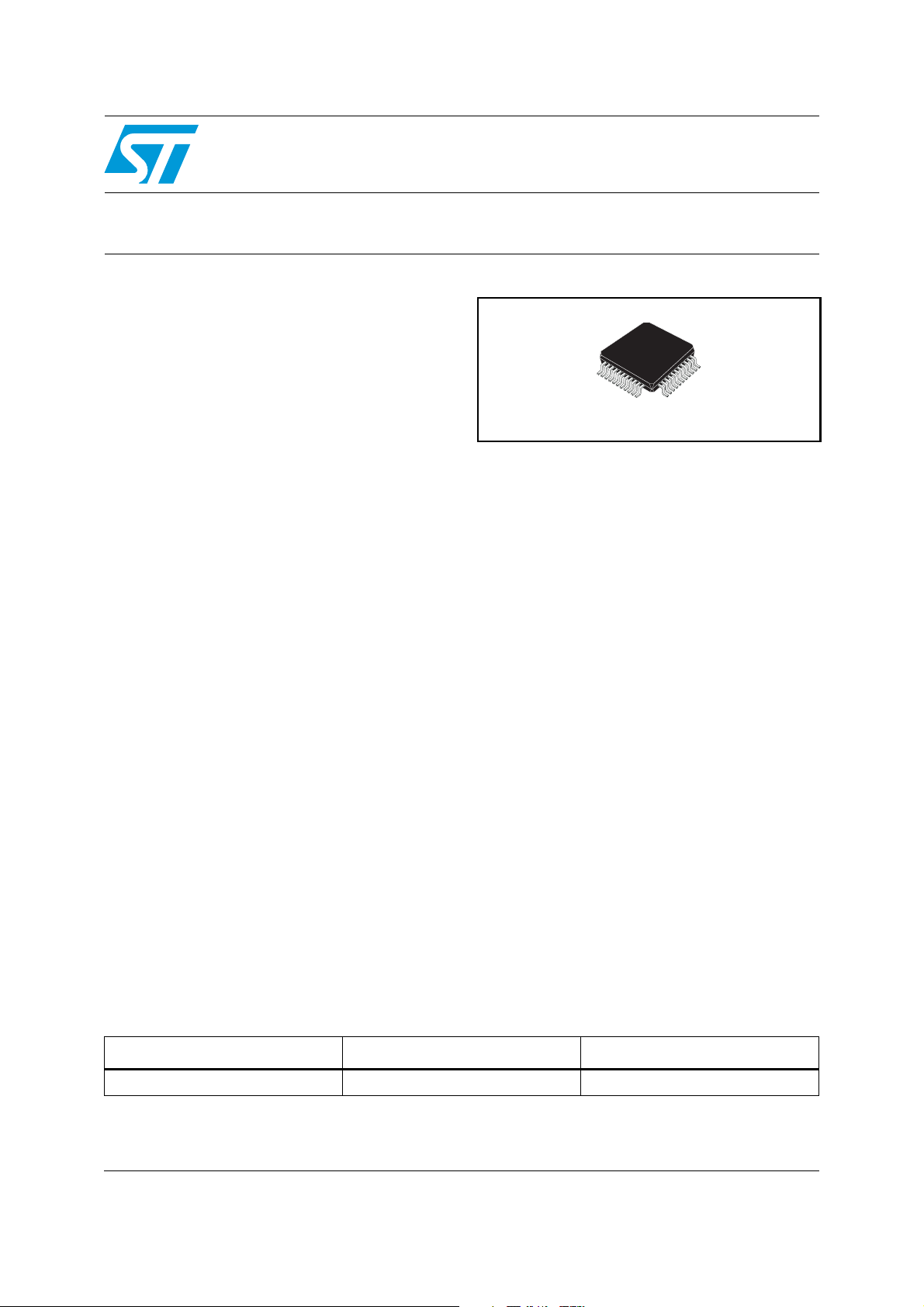
LQFP44
generate the negative battery by means of an
on chip DC/DC converter controller that drives an
external MOS switch.
The battery level is properly adjusted depending
on the operating mode. A useful characteristic for
these applications is the integrated ringing
generator.
The control interface is a parallel type with open
drain output and 3.3 V logic levels.
The metering pulses are generated on chip
starting from two logic signals (0 and 3.3 V) one
define the metering pulse frequency and the other
the metering pulse duration. An on chip circuit
then provides the proper shaping and filtering.
Metering pulse amplitude and shaping (rising and
decay time) can be programmed by external
components. A dedicated cancellation circuit
avoid possible codec input saturation due to
metering pulse echo.
Description
The STLC3055N is a SLIC device specifically
designed for wireless local loop (WLL) and ISDNterminal adaptors (ISDN-TA) and VoIP
applications. One of the distinctive characteristic
of this device is the ability to operate with a single
supply voltage (from 5.5 V to 12 V) and self
Table 1. Device summary
Order code
E-STLC3055N
1. ECOPACK® (see Section 10)
February 2009 Rev 11 1/34
(1)
Constant current feed can be set from 20 mA to
40 mA. Off-hook detection threshold is
programmable from 5 mA to 9 mA.
The device, developed in BCD III S technology
(90 V process), operates in the extended
temperature range and integrates a thermal
protection that sets the device in power down
when T
Package Packing
LQFP44 Tray
exceeds 140 °C.
j
www.st.com
1
Page 2

Contents STLC3055N
Contents
1 Block diagram . . . . . . . . . . . . . . . . . . . . . . . . . . . . . . . . . . . . . . . . . . . . . . 5
2 Pin description . . . . . . . . . . . . . . . . . . . . . . . . . . . . . . . . . . . . . . . . . . . . . 6
3 Electrical specification . . . . . . . . . . . . . . . . . . . . . . . . . . . . . . . . . . . . . . . 8
3.1 Absolute maximum rating . . . . . . . . . . . . . . . . . . . . . . . . . . . . . . . . . . . . . . 8
3.2 Operating range . . . . . . . . . . . . . . . . . . . . . . . . . . . . . . . . . . . . . . . . . . . . . 8
3.3 Thermal data . . . . . . . . . . . . . . . . . . . . . . . . . . . . . . . . . . . . . . . . . . . . . . . 8
4 Functional description . . . . . . . . . . . . . . . . . . . . . . . . . . . . . . . . . . . . . . . 9
4.1 DC/DC converter . . . . . . . . . . . . . . . . . . . . . . . . . . . . . . . . . . . . . . . . . . . . 9
4.2 Operating modes . . . . . . . . . . . . . . . . . . . . . . . . . . . . . . . . . . . . . . . . . . . 10
4.2.1 Power down . . . . . . . . . . . . . . . . . . . . . . . . . . . . . . . . . . . . . . . . . . . . . . 10
4.2.2 High impedance feeding (HI-Z) . . . . . . . . . . . . . . . . . . . . . . . . . . . . . . . 10
4.2.3 Active . . . . . . . . . . . . . . . . . . . . . . . . . . . . . . . . . . . . . . . . . . . . . . . . . . . 10
4.2.4 Ringing . . . . . . . . . . . . . . . . . . . . . . . . . . . . . . . . . . . . . . . . . . . . . . . . . . 13
5 Application information . . . . . . . . . . . . . . . . . . . . . . . . . . . . . . . . . . . . . 16
5.1 Layout recommendation . . . . . . . . . . . . . . . . . . . . . . . . . . . . . . . . . . . . . . 16
5.2 External components list . . . . . . . . . . . . . . . . . . . . . . . . . . . . . . . . . . . . . 17
5.3 Application diagram . . . . . . . . . . . . . . . . . . . . . . . . . . . . . . . . . . . . . . . . . 20
6 Electrical characteristics . . . . . . . . . . . . . . . . . . . . . . . . . . . . . . . . . . . . 22
6.1 Test circuits . . . . . . . . . . . . . . . . . . . . . . . . . . . . . . . . . . . . . . . . . . . . . . . . 26
7 Overvoltage protection . . . . . . . . . . . . . . . . . . . . . . . . . . . . . . . . . . . . . . 29
8 Typical state diagram for STLC3055N operation . . . . . . . . . . . . . . . . . 30
9 STLC3055Q vs STLC3055N compatibility. . . . . . . . . . . . . . . . . . . . . . . 31
9.1 Typical power consumption comparison . . . . . . . . . . . . . . . . . . . . . . . . . . 31
9.2 Hardware differences . . . . . . . . . . . . . . . . . . . . . . . . . . . . . . . . . . . . . . . . 31
9.3 Parameter differences . . . . . . . . . . . . . . . . . . . . . . . . . . . . . . . . . . . . . . . 31
10 Package information . . . . . . . . . . . . . . . . . . . . . . . . . . . . . . . . . . . . . . . . 32
11 Revision history . . . . . . . . . . . . . . . . . . . . . . . . . . . . . . . . . . . . . . . . . . . 33
2/34
Page 3

STLC3055N List of tables
List of tables
Table 1. Device summary . . . . . . . . . . . . . . . . . . . . . . . . . . . . . . . . . . . . . . . . . . . . . . . . . . . . . . . . . . 1
Table 2. Pin description . . . . . . . . . . . . . . . . . . . . . . . . . . . . . . . . . . . . . . . . . . . . . . . . . . . . . . . . . . . 6
Table 3. Absolute maximum ratings . . . . . . . . . . . . . . . . . . . . . . . . . . . . . . . . . . . . . . . . . . . . . . . . . . 8
Table 4. Operating range . . . . . . . . . . . . . . . . . . . . . . . . . . . . . . . . . . . . . . . . . . . . . . . . . . . . . . . . . . 8
Table 5. Thermal data. . . . . . . . . . . . . . . . . . . . . . . . . . . . . . . . . . . . . . . . . . . . . . . . . . . . . . . . . . . . . 8
Table 6. SLIC operating modes. . . . . . . . . . . . . . . . . . . . . . . . . . . . . . . . . . . . . . . . . . . . . . . . . . . . . . 9
Table 7. Gain set in active mode . . . . . . . . . . . . . . . . . . . . . . . . . . . . . . . . . . . . . . . . . . . . . . . . . . . 11
Table 8. SLIC states in active mode . . . . . . . . . . . . . . . . . . . . . . . . . . . . . . . . . . . . . . . . . . . . . . . . . 12
Table 9. CREST factor . . . . . . . . . . . . . . . . . . . . . . . . . . . . . . . . . . . . . . . . . . . . . . . . . . . . . . . . . . . 14
Table 10. External components . . . . . . . . . . . . . . . . . . . . . . . . . . . . . . . . . . . . . . . . . . . . . . . . . . . . . 17
Table 11. External components @gain set = 0. . . . . . . . . . . . . . . . . . . . . . . . . . . . . . . . . . . . . . . . . . 18
Table 12. External components @gain set = 1. . . . . . . . . . . . . . . . . . . . . . . . . . . . . . . . . . . . . . . . . . 19
Table 13. Electrical characteristics . . . . . . . . . . . . . . . . . . . . . . . . . . . . . . . . . . . . . . . . . . . . . . . . . . . 22
Table 14. Power consumption differences . . . . . . . . . . . . . . . . . . . . . . . . . . . . . . . . . . . . . . . . . . . . . 31
Table 15. Hardware differences . . . . . . . . . . . . . . . . . . . . . . . . . . . . . . . . . . . . . . . . . . . . . . . . . . . . . 31
Table 16. Parameter differences . . . . . . . . . . . . . . . . . . . . . . . . . . . . . . . . . . . . . . . . . . . . . . . . . . . . 31
Table 17. Document revision history . . . . . . . . . . . . . . . . . . . . . . . . . . . . . . . . . . . . . . . . . . . . . . . . . 33
3/34
Page 4

List of figures STLC3055N
List of figures
Figure 1. Block diagram . . . . . . . . . . . . . . . . . . . . . . . . . . . . . . . . . . . . . . . . . . . . . . . . . . . . . . . . . . . . 5
Figure 2. Pin connection (top view) . . . . . . . . . . . . . . . . . . . . . . . . . . . . . . . . . . . . . . . . . . . . . . . . . . . 6
Figure 3. DC characteristic in HI-Z mode. . . . . . . . . . . . . . . . . . . . . . . . . . . . . . . . . . . . . . . . . . . . . . 10
Figure 4. DC characteristic in active mode . . . . . . . . . . . . . . . . . . . . . . . . . . . . . . . . . . . . . . . . . . . . 11
Figure 5. TIP/RING typical transition from direct to reverse polarity . . . . . . . . . . . . . . . . . . . . . . . . . 12
Figure 6. Metering pulse generation circuit. . . . . . . . . . . . . . . . . . . . . . . . . . . . . . . . . . . . . . . . . . . . . 13
Figure 7. TIP/RING typical ringing waveform. . . . . . . . . . . . . . . . . . . . . . . . . . . . . . . . . . . . . . . . . . . 14
Figure 8. Application diagram with metering pulse generation. . . . . . . . . . . . . . . . . . . . . . . . . . . . . . 20
Figure 9. Application diagram without metering pulse generation . . . . . . . . . . . . . . . . . . . . . . . . . . . 21
Figure 10. 2W return loss 2WRL = 20Log(|Zref + Zs|/|Zref-Zs|) = 20Log(E/2Vs) . . . . . . . . . . . . . . . . 26
Figure 11. THL trans hybrid loss THL = 20Log|Vrx/Vtx|. . . . . . . . . . . . . . . . . . . . . . . . . . . . . . . . . . . . 26
Figure 12. G24 transmit gain G24 = 20Log|2Vtx/E| . . . . . . . . . . . . . . . . . . . . . . . . . . . . . . . . . . . . . . . 26
Figure 13. G42 receive gain G42 = 20Log|VI/Vrx| . . . . . . . . . . . . . . . . . . . . . . . . . . . . . . . . . . . . . . . . 27
Figure 14. PSRRC power supply rejection Vpos to 2W port PSSRC = 20Log|Vn/Vl| . . . . . . . . . . . . . 27
Figure 15. L/T longitudinal to transversal conversion L/T = 20Log|Vcm/Vl| . . . . . . . . . . . . . . . . . . . . . 27
Figure 16. T/L transversal to longitudinal conversion T/L = 20Log|Vrx/Vcm|. . . . . . . . . . . . . . . . . . . . 28
Figure 17. VTTX metering pulse level on line . . . . . . . . . . . . . . . . . . . . . . . . . . . . . . . . . . . . . . . . . . . 28
Figure 18. V2Wp and W4Wp: idle channel psophometric noise at line and TX.
V2Wp = 20Log|Vl/0.774l|; V4Wp = 20Log|Vtx/0.774l| . . . . . . . . . . . . . . . . . . . . . . . . . . . . 28
Figure 19. Simplified configuration for indoor overvoltage protection . . . . . . . . . . . . . . . . . . . . . . . . . 29
Figure 20. Standard overvoltage protection configuration for K20 compliance . . . . . . . . . . . . . . . . . . 29
Figure 21. State diagram . . . . . . . . . . . . . . . . . . . . . . . . . . . . . . . . . . . . . . . . . . . . . . . . . . . . . . . . . . . 30
Figure 22. LQFP44 (10 x 10 x 1.4 mm) mechanical data and package dimensions . . . . . . . . . . . . . . 32
4/34
Page 5

STLC3055N Block diagram
1 Block diagram
Figure 1. Block diagram
PD D0 D1 D2 DET
GAIN
SETTING
TX
RX
ZAC1
ZAC
RS
ZB
CKTTX
CTTX1
CTTX2
FTTX
INPUT LOGIC AND DECODER
Status and functions
SUPERVISION
AC PROC
TTX PROC
RTTX CAC ILTF RD IREF RLIM RTH
REFERENCE
OUTPUT LOGIC
LINE
DRIVER
Vcc
Vss
Agnd
OUTPUT
STAGE
DC PROC
DC/DC
CONV.
VOLT.
REG.
AGND
BGND
TIP
RING
CREV
CSVR
CLK
RSENSE
GATE
VF
CVCC
VPOS
VBAT
Vbat
5/34
Page 6

Pin description STLC3055N
2 Pin description
Figure 2. Pin connection (top view)
VBAT1
CREV
N.C.
TIP
N.C.
N.C.
RING
N.C.
VBAT
BGND
33
CSVR
32
ILTF
31
RD
30
RTH
29
IREF
28
RLIM
27
AGND
26
CVCC
25
VPOS
24
RSENSE
23
GATE
TX
D00TL488-MOD
VF
CLK
GAIN SET
N.C.
N.C.
DET
CKTTX
CTTX1
CTTX2
44 43 42 413940 38 37 36 35 34
1
D0
2
D1
3
D2
4
PD
5
6
7
8
9
10
12 13 14 15 16
RX
RTTX
FTTX
ZAC1
ZAC
N.C.
171118 19 20 21 22
ZB
RS
CAC
Table 2. Pin description
N° Pin Function
1 D0 Control Interface: input bit 0.
2 D1 Control Interface: input bit 1.
3 D2 Control interface: input bit 2.
4 PD Power down input. Normally connected to CVCC (or to logic level high).
5 Gain SET
6,7,36,
38,39,40,42
Control gain interface: 0 Level R
NC Not connected.
1 Level R
= 0dB T
xgain
= +6dB T
xgain
xgain
xgain
= -6dB
= -12dB
8 DET Logic interface output of the supervision detector (active low).
9 CKTTX Metering pulse clock input (12 KHz or 16KHz square wave).
10 CTTX1 Metering burst shaping external capacitor.
11 CTTX2 Metering burst shaping external capacitor.
12 RTTX
13 FTTX
Metering pulse cancellation buffer output. TTX filter network should be connected to
this point. If not used should be left open.
Metering pulse buffer input this signal is sent to the line and used to perform TTX
filtering.
4 wire input port (RX input). A 100 kΩ external resistor must be connected to AGND to
14 RX
bias the input stage. This signal is referred to AGND. If connected to single supply
CODEC output it must be DC decoupled with proper capacitor.
15 ZAC1 RX buffer output, (the AC impedance is connected from this node to ZAC).
16 ZAC AC impedance synthesis.
6/34
Page 7
STLC3055N Pin description
Table 2. Pin description (continued)
N° Pin Function
17 RS Protection resistors image (the image resistor is connected from this node to ZAC).
18 ZB
19 CAC AC feedback input, AC/DC split capacitor (CAC).
20 TX
21 VF Feedback input for DC/DC converter controller.
22 CLK
23 GATE Driver for external Power MOS transistor (P-channel).
24 RSENSE
25 VPOS Positive supply
26 CVCC Internal positive voltage supply filter.
27 AGND Analog ground, must be shorted with BGND.
28 RLIM
29 IREF
30 RTH
Balance network for 2 to 4 wire conversion (the balance impedance ZB is connected
from this node to AGND. ZA impedance is connected from this node to ZAC1).
4 wire output port (TX output). The signal is referred to AGND. If connected to single
supply CODEC input it must be DC decoupled with proper capacitor.
Power switch controller clock (typ. 125 kHz). This pin can also be connected to CVCC
or AGND. When the CLK pin is connected to CVCC an auto-oscillation is internally
generated and it is used instead of the external clock. When the CLK pin is connected
to AGND, the GATE output is disabled.
Voltage input for current sensing. RSENSE should be connected close to this pin and
VPOS pin. The PCB layout should minimize the extra resistance introduced by the
copper tracks.
Constant current feed programming pin (via RLIM). RLIM should be connected close to
this pin and AGND pin to avoid noise injection.
Internal bias current setting pin. RREF should be connected close to this pin and
AGND pin to avoid noise injection.
Off-hook threshold programming pin (via RTH). RTH should be connected close to this
pin and AGND pin to avoid noise injection.
31 RD
32 ILTF Transversal line current image output.
33 CSVR Battery supply filter capacitor.
34 BGND Battery ground, must be shorted with AGND.
35 VBAT
37 RING 2 wire port; RING wire (Ib is the current sunk into this pin).
41 TIP 2 wire port; TIP wire (Ia is the current sourced from this pin).
43 CREV
44 VBAT1 Frame connection. Must be shorted to VBAT.
DC feedback and ring trip input. RD should be connected close to this pin and AGND
pin to avoid noise injection.
Regulated battery voltage self generated by the device via DC/DC converter. Must be
shorted to VBAT1.
Reverse polarity transition time control. One proper capacitor connected between this
pin and AGND is setting the reverse polarity transition time. This is the same transition
time used to shape the "trapezoidal ringing" during ringing injection.
7/34
Page 8
Electrical specification STLC3055N
3 Electrical specification
3.1 Absolute maximum rating
Table 3. Absolute maximum ratings
Symbol Parameter Value Unit
V
Positive supply voltage -0.4 to +13 V
pos
A/BGND AGND to BGND -1 to +1 V
V
V
btot
ESD
RATING
1. Vbat is self generated by the on chip DC/DC converter and can be programmed via RF1 and RF2.
RF1 and RF2 shall be selected in order to fulfil the a.m limits (see Table 10: External components on
page 17).
Pin D0, D1, D2, DET, CKTTX -0.4 to 5.5 V
dig
T
Max. junction temperature 150 °C
j
Vbtot=|Vpos|+|Vbat|. (Total voltage applied to the device
(1)
supply pins).
Human body model ±1750 V
Charged device model ±500 V
3.2 Operating range
Table 4. Operating range
Symbol Parameter Value Unit
V
A/BGND AGND to BGND -100 to +100 mV
V
T
V
bat
1. Vbat is self generated by the on chip DC/DC converter and can be programmed via RF1 and RF2.
RF1 and RF2 shall be selected in order to fulfill the a.m limits (see Table 10: External components on
page 17).
Positive supply voltage 5.5 to +12 V
pos
Pin D0, D1, D2, DET, CKTTX, PD -0.25 to 5.25 V
dig
Ambient operating temperature range -40 to +85 °C
op
(1)
Self generated battery voltage -74 max. V
90 V
3.3 Thermal data
Table 5. Thermal data
Symbol Parameter Value Unit
R
th j-amb
8/34
Thermal resistance junction to ambient Typ. 60 °C/W
Page 9

STLC3055N Functional description
4 Functional description
The STLC3055N is a device specifically developed for WLL VoIP and ISDN-TA applications.
It is based on a SLIC core, on purpose optimised for these applications, with the addition of
a DC/DC converter controller to fulfil the WLL and ISDN-TA design requirements.
The SLIC performs the standard feeding, signalling and transmission functions.
It can be set in four different operating modes via the D0, D1, D2 pins of the control logic
interface (0 to 3.3 V logic levels). The loop status is carried out on the DET
pin (active low).
The DET
pin is an open drain output to allow easy interfacing with both 3.3 V and 5 V logic
levels.
The four possible SLIC’s operating modes are:
● Power down
● High impedance feeding (HI-Z)
● Active
● Ringing
Ta bl e 6 shows how to set the different SLIC operating modes.
Table 6. SLIC operating modes.
PD D0 D1 D2 Operating mode
000XPower down
1 0 0 X H.I. feeding (HI-Z)
1 0 1 0 Active normal polarity
1011Active reverse polarity
1 1 1 0 Active TTX injection (N.P.)
1 1 1 1 Active TTX injection (R.P.)
1 1 0 0/1 Ring (D2 bit toggles @ fring)
4.1 DC/DC converter
The DC/DC converter controller is driving an external power MOS transistor (P-channel) in
order to generate the negative battery voltage needed for device operation.
The DC/DC converter controller is synchronised with an external CLK (125 kHz typ.) or with
an internal clock generated when the pin CLK is connected to CVCC. One sensing resistor
in series to Vpos supply allows to fix the maximum allowed input peak current. This feature
is implemented in order to avoid overload on Vpos supply in case of line transient (ex. ring
trip detection).
The typical value is obtained for a sensing resistor equal to 110 mΩ that will guarantee an
average current consumption from Vpos < 700 mA. When in on-hook the self generated
battery voltage is set to a predefined value.
This value can be adjusted via one external resistor (RF1) and it is typical -50 V. When
RING mode is selected this value is increased to -70 V typ.
9/34
Page 10

Functional description STLC3055N
Once the line goes in off-hook condition, the DC/DC converter automatically adjust the
generated battery voltage in order to feed the line with a fixed DC current (programmable via
RLIM) optimising in this way the power dissipation.
4.2 Operating modes
4.2.1 Power down
When this mode is selected the SLIC is switched off and the TIP and RING pins are in high
impedance. Also the line detectors are disabled therefore the off-hook condition cannot be
detected.
This mode can be selected in emergency condition when it is necessary to cut any current
delivered to the line.
This mode is also forced by STLC3055N in case of thermal overload (T
In this case the device goes back to the previous status as soon as the junction temperature
decrease under the hysteresis threshold.
No AC transmission is possible in this mode.
4.2.2 High impedance feeding (HI-Z)
This operating mode is normally selected when the telephone is in on-hook in order to
monitor the line status keeping the power consumption at the minimum.
The output voltage in on-hook condition is equal to the self generated battery voltage (-50 V
typ).
When off-hook occurs the DET
The off-hook threshold in HI-Z mode is the same value as programmed in ACTIVE mode.
The DC characteristic in HI-Z mode is just equal to the self generated battery with
2x(1600 Ω+Rp) in series (see Figure 3), where Rp is the external protection resistance.
No AC transmission is possible in this mode.
Figure 3. DC characteristic in HI-Z mode.
becomes active (low logic level).
IL
Vbat
2x(R1+Rp)
Slope: 2x(R1+Rp)
(R1=1600ohm)
> 140 °C).
j
4.2.3 Active
DC characteristics and supervision
When this mode is selected the STLC3055N provides both DC feeding and AC
transmission.
10/34
VL
Vbat (-50V)
Page 11

STLC3055N Functional description
The STLC3055N feeds the line with a constant current fixed by RLIM (20 mA to 40 mA
range). The on-hook voltage is typically 40 V allowing on-hook transmission; the self
generated Vbat is -50 V typ.
If the loop resistance is very high and the line current cannot reach the programmed
constant current feed value, the STLC3055N behaves like a 40 V voltage source with a
series impedance equal to the protection resistors 2xRp (typ. 2 x 50 Ω). Figure 4 shows the
typical DC characteristic in Active mode.
Figure 4. DC characteristic in active mode
IL
Ilim
(20 to
40mA)
2Rp
10V
Vbat (-50V)
VL
The line status (on/off-hook) is monitored by the SLIC’s supervision circuit. The off-hook
threshold can be programmed via the external resistor RTH in the range from 5 mA to 9 mA.
Independently on the programmed constant current value, the TIP and RING buffers have a
current source capability limited to 80 mA typ. Moreover the power available at Vbat is
controlled by the DC/DC converter that limits the peak current drawn from the Vpos supply.
The maximum allowed current peak is set by R
SENSE
resistor.
AC characteristics
The SLIC provides the standard SLIC transmission functions:
Once in active mode the SLIC can operate with two different Tx, Rx Gain. Setting properly
by the gain set control bit (see Ta bl e 7 ).
Table 7. Gain set in active mode
Gain set 4 to 2 wire gain 2 to 4 wire gain Impedance synthesis scale factor
0 0 dB -6 dB x 50
1 +6 dB -12 dB x 25
● Input impedance synthesis: can be real or complex and is set by a scaled (x 50 or
x 25) external ZAC impedance.
● Transmit and receive: The AC signal present on the 2W port (TIP and RING pins) is
transferred to the TX output with a -6 dB or -12 dB gain and from the RX input to the
2W port with a 0 dB or +6 dB gain.
● 2 to 4 wire conversion: The balance impedance can be real or complex, the proper
cancellation is obtained by means of two external impedance ZA and ZB
Once in Active mode (D1=1) the SLIC can operate in different states setting properly D0 and
D2 control bits (see also Ta bl e 8 ).
11/34
Page 12
Functional description STLC3055N
Table 8. SLIC states in active mode
D0 D1 D2 Operating Mode
0 1 0 Active normal polarity
0 1 1 Active reverse polarity
1 1 0 Active TTX injection (normal polarity)
1 1 1 Active TTX injection (reverse polarity)
Polarity reversal
The D2 bit controls the line polarity, the transition between the two polarities is performed in
a "soft" way. This means that the TIP and RING wire exchange their polarities following a
ramp transition (see Figure 5). The transition time is controlled by an external capacitor
CREV. This capacitor is also setting the shape of the ringing trapezoidal waveform. When
the control pins set battery reversal the line polarity is reversed with a proper transition time
set via an external capacitor (CREV).
Figure 5. TIP/RING typical transition from direct to reverse polarity
GND
TIP
RING
4V typ.
40V typ
ON-HOOK
dV/dT set
by CREV
Metering pulse injection (Ttx)
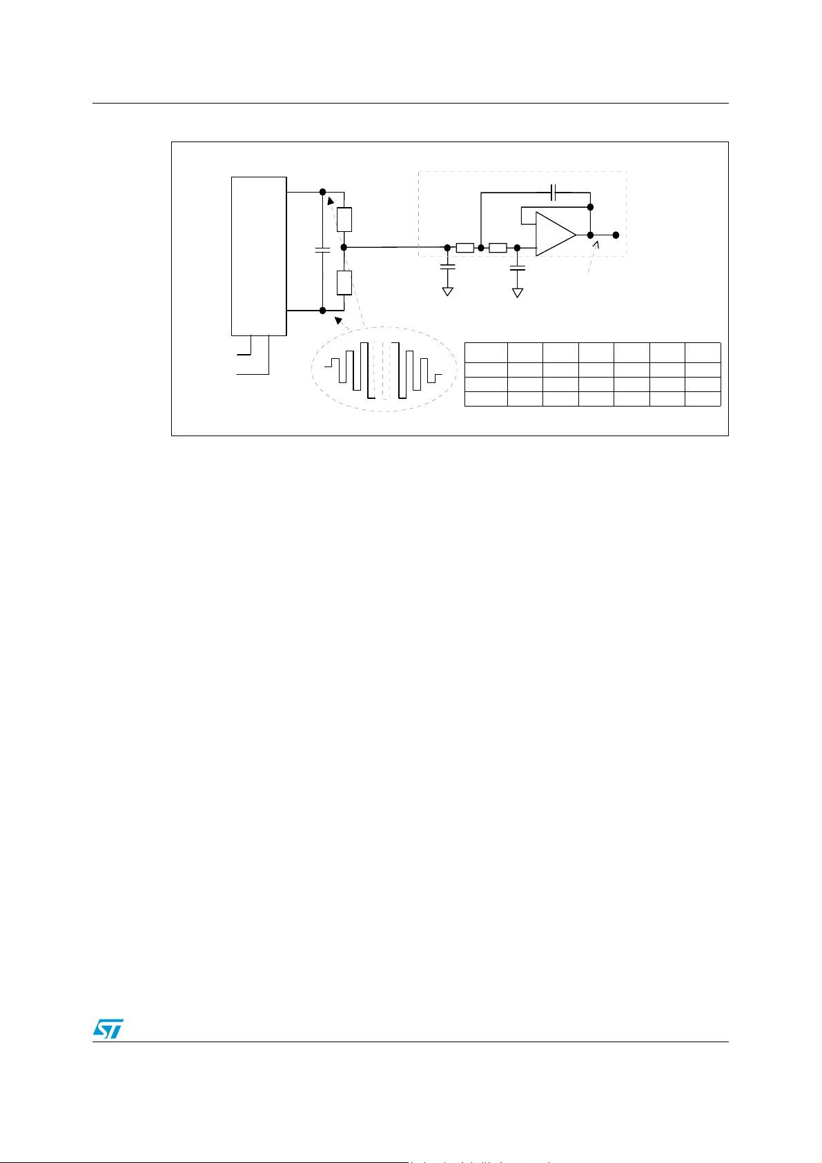
The metering pulses circuit consists of a burst shaping generator that gives a square wave
shaped and a low pass filter to reduce the harmonic distortion of the output signal.
The metering pulse is obtained starting from two logic signals:
● CKTTX: is a square wave at the TTX frequency (12 or 16 kHz) and should be
permanently applied to the CKTTX pin or at least for all the duration of the TTX pulse
(including rising and decay phases).
● D0: enable the TTX generation circuit and define the TTX pulse duration.
These two signals are processed by a dedicated circuitry integrated on chip that generate
the metering pulse as an amplitude modulated shaped squarewave (SQTTX)
(see Figure 6).
Both the amplitude and the envelope of the squarewave (SQTTX) can be programmed by
means of external components. In particular the amplitude is set by the two resistors RLV
and the shaping by the capacitor CS.
12/34
Page 13
STLC3055N Functional description
Figure 6. Metering pulse generation circuit.
Low Pass Filter
CTTX1
C1
BURST
SHAPING
GENERAT OR
D0
CKTTX
Square wave pulse metering
CS
CTTX2
RLV
SQTTX
RLV
FTTX
OP1
+
C2
Sinusoidal wave
pulse metering
R2
R1
CFL
Required external components vs. filter order.
Order CFL R1 C1 R2 C2 THD
1 X13%
2 XXXX6%
3 XXXXX3%
RTTX
The waveform so generated is then filtered and injected on the line.
The low pass filter can be obtained using the integrated buffer OP1 connected between pin
FTTX (OP1 non inverting input) and RTTX (OP1 output) (see Figure 6) and implementing a
"Sallen and Key" configuration. Depending on the external components count it is possible
to build an optimised application depending on the distortion level required. In particular
harmonic distortion levels equal to 13 %, 6 % and 3 % can be obtained respectively with
first, second and third order filters (see Figure 6).
The circuit showed in Figure 8: Application diagram with metering pulse generation. on
page 20 is related to the simple first order filter.
Once the shaped and filtered signal is obtained at RTTX buffer output it is injected on the
TIP/RING pins with a +6 dB gain or +12 dB gain.
It should be noted that this is the nominal condition obtained in presence of ideal TTX echo
cancellation (obtained via proper setting of RTTX and CTTX).
In addition, the effective level obtained on the line will depend on the line impedance and the
protection resistors value. In the typical application (TTX line impedance =200 Ω, RP = 50 Ω,
and ideal TTX echo cancellation) the metering pulse level on the line will be 1.33 or 2.66
times the level applied to the RTTX pin.
As already mentioned the metering pulse echo cancellation is obtained by means of two
external components (RTTX and CTTX) that should match the line impedance at the TTX
frequency. This simple network has a double effect:
● Synthesize a low output impedance at the TIP/RING pins at the TTX frequency.
● Cut the eventual TTX echo that will be transferred from the line to the TX output.
4.2.4 Ringing
When this mode is selected STLC3055N self generate an higher negative battery (-70 V
typ.) in order to allow a balanced ringing signal of typically 65 Vpeak.
In this condition both the DC and AC feedback are disabled and the SLIC line drivers
operate as voltage buffers. The ring waveform is obtained toggling the D2 control bit at the
13/34
Page 14
Functional description STLC3055N
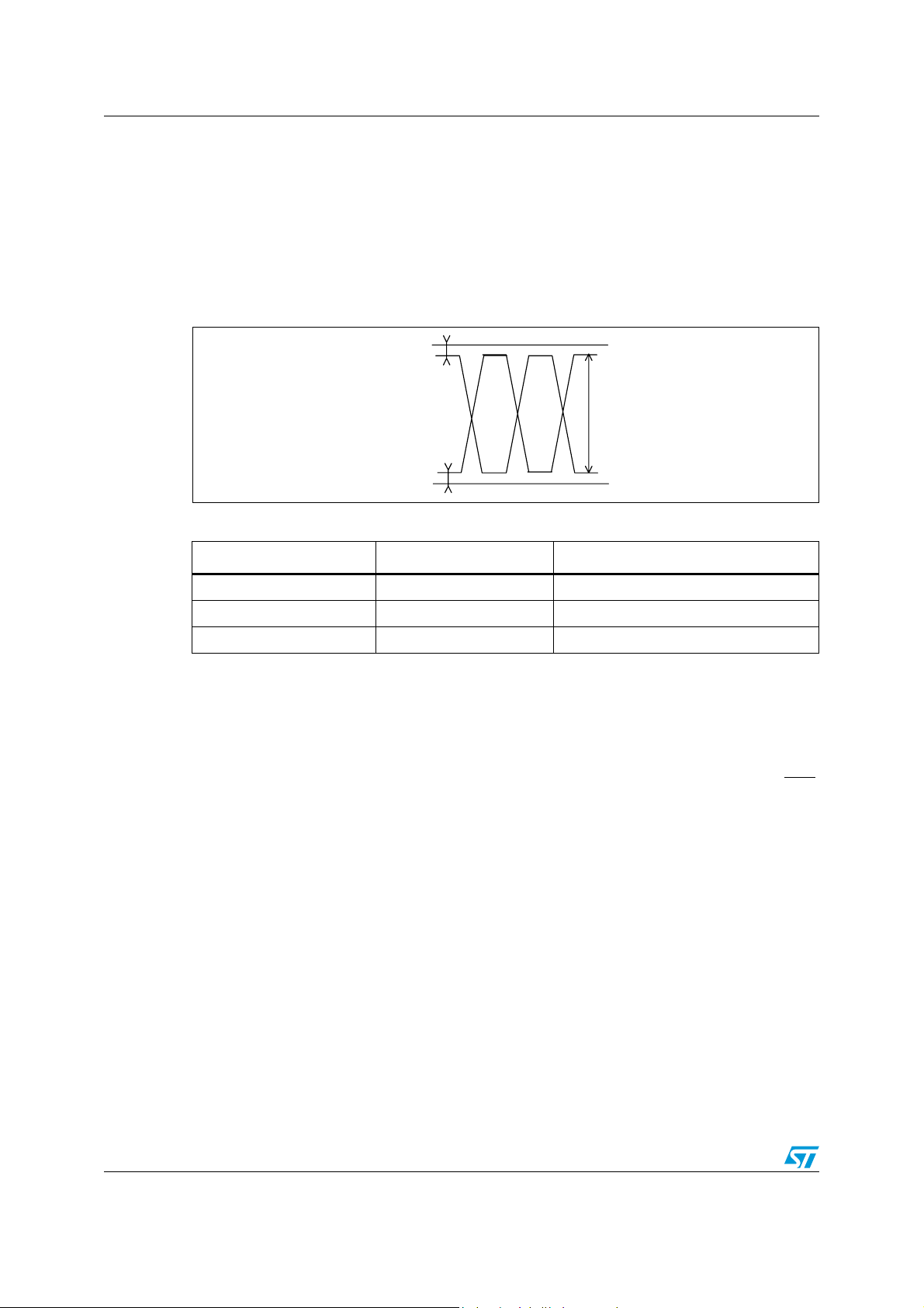
desired ring frequency. This bit in fact controls the line polarity (0=direct; 1=reverse). As in
the Active mode the line voltage transition is performed with a ramp transition, obtaining in
this way a trapezoidal balanced ring waveform (see Figure 7). The shaping is defined by the
CREV external capacitor.
Selecting the proper capacitor value it is possible to get different CREST factor values.
The following table shows the CREST factor values obtained with a 20 Hz and 25 Hz ring
frequency and with 1REN. These value are valid either with European or USA specification.
Figure 7. TIP/RING typical ringing waveform
Table 9. CREST factor
GND
TIP
RING
VBAT
2.5V typ.
dV/dT set
by CREV
2.5V typ.
65V
typ.
CREV CREST factor @20 Hz CREST factor @25 Hz
22nF 1.2 1.26
27nF 1.25 1.32
33nF 1.33 Not significant
1. Distortion already less than 10%.
(1)
The ring trip detection is performed sensing the variation of the AC line impedance from onhook (relatively high) to off-hook (low). This particular ring trip method allows to operate
without DC offset superimposed on the ring signal and therefore obtaining the maximum
possible ring level on the load starting from a given negative battery. It should be noted that
such a method is optimised for operation on short loop applications and may not operate
properly in presence of long loop applications (> 500 Ω). Once ring trip is detected, the DET
output is activated (logic level low), at this point the card controller or a simple logic circuit
should stop the D2 toggling in order to effectively disconnect the ring signal and then set the
STLC3055N in the proper operating mode (normally Active).
Ring level in presence of more telephone in parallel
As already mentioned above the maximum current that can be drawn from the Vpos supply
is controlled and limited via the external R
the self generated negative battery.
If for any reason the ringer load will be too low the self generated battery will drop in order to
keep the power consumption to the fixed limit and therefore also the ring voltage level will be
reduced.
In the typical application with R
about 900 mA, which correspond to an average current of 700 mA max. In this condition the
STLC3055N can drive up to 3REN with a ring frequency fr=25 Hz (1REN = 1800 Ω + 1.0 µF,
European standard).
14/34
= 110 mΩ the peak current from Vpos is limited to
SENSE
. This will limit also the power available at
SENSE
Page 15

STLC3055N Functional description
In order to drive up to 5REN (1REN= 6930 Ω + 8 µF, US standard) it is necessary to modify
the external components as follows:
CREV = 15 nF
RD = 2.2 kΩ
Rsense = 100 mΩ .
15/34
Page 16

Application information STLC3055N
5 Application information
5.1 Layout recommendation
A properly designed PCB layout is a basic issue to guarantee a correct behavior and good
noise performances. Noise sources can be identified in not enough good grounds, not
enough low impedance supplies and parasitic coupling between PCB tracks and high
impedance pins of the device.
Particular care must be taken on the ground connection and in this case the star
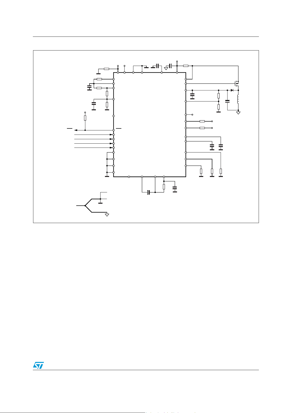
configuration allows surely to avoid possible problems (see Figure 8 on page 20 and
Figure 9 on page 21).
The ground of the power supply (VPOS) has to be connected to the center of the star, let’s
call this point Supply GND. This point should show a resistance as low as possible, that
means it should be a ground plane.
In particular to avoid noise problems the layout should prevent any coupling between the
DC/DC converter components that are referred to PGND (CVPOS, CD, L) and analog pins
that are referred to AGND (ex: RD, IREF, RTH, RLIM, VF). AGND and BGND must be
shorter together. The GND connection of protection components have to be connected to
the Supply GDND.
As a first recommendation the components CV, L, D1, CVPOS, RSENSE should be kept as
close as possible to each other and isolated from the other components.
Additional improvements can be obtained:
● decoupling the center of the star from the analog ground of STLC3055N using small
chokes.
● adding a capacitor in the range of 100 nF between VPOS and AGND in order to filter
the switch frequency on VPOS.
16/34
Page 17
STLC3055N Application information
5.2 External components list
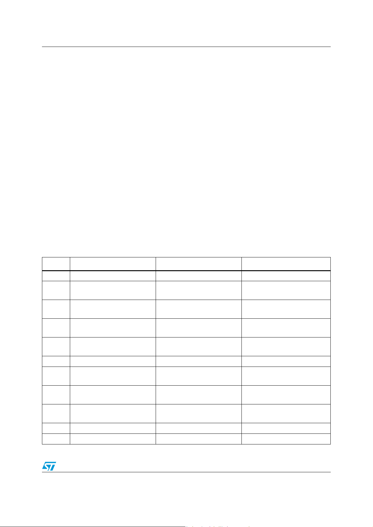
In order to properly define the external components value the following system parameters
have to be defined:
● The AC input impedance shown by the SLIC at the line terminals "Zs" to which the
return loss measurement is referred. It can be real (typ. 600 Ω) or complex.
● The AC balance impedance, it is the equivalent impedance of the line "Zl" used for
evaluation of the trans-hybrid loss performances (2/4 wire conversion). It is usually a
complex impedance.
● The value of the two protection resistors Rp in series with the line termination. The line
impedance at the TTX frequency "Zlttx".
● The metering pulse level amplitude measured at line termination "VLOTTX". In case of
low order filtering, VLOTTX represents the amplitude (Vrms) of the fundamental
frequency component. (typ 12 or 16 kHz).
● Pulse metering envelope rise and decay time constant "τ".
●
The slope of the ringing waveform "ΔVTR/ΔT ".
● The value of the constant current limit current "Ilim".
● The value of the off-hook current threshold "I
● The value of the ring trip rectified average threshold current "I
● The value of the required self generated negative battery "V
value is 70 V). This value can be obtained from the desired ring peak level +5 V.
● The value of the maximum current peak sunk from Vpos "IPK".
Table 10. External components
TH
".
".
RTH
" in ring mode (max
BATR
Name Function Formula Typ. value
RRX Rx input bias resistor 100 kΩ 5%
RREF Bias setting current
CSVR Negative battery filter
RD
Ring Trip threshold setting
resistor
CAC AC/DC split capacitance
RREF = 1.3/Ibias
Ibias = 50 μA
CSVR = 1/(2π ⋅ fp ⋅ 1.8 MΩ)
fp = 50 Hz
RD = 100/I
RTH
2kΩ < RD < 5 kΩ
26 kΩ 1%
1.5 nF 10%
100 V
4.12 kΩ 1%
@ IRTH = 24 mA
22 μF 20% 15 V
@ RD = 4.12 kΩ
RP Line protection resistor Rp > 30 Ω 50 Ω 1%
RLIM Current limiting programming
RTH
CREV
Off-hook threshold programming
(ACTIVE mode)
Reverse polarity transition time
programming
RLIM = 1300/Ilim
32.5kΩ < RLIM < 65kΩ
RTH = 290/I
TH
27 kΩ < RTH < 52 kΩ
CREV = ((1/3750) · ΔT/ΔV
TR
)
52.3 kΩ 1%
@ Ilim = 25 mA
32.4 kΩ 1%
@ITH = 9 mA
22 nF 10% 10 V
@ 12 V/ms
RDD Pull up resistors 100 kΩ
CVCC Internally supply filter capacitor 100 nF 20% 10 V
17/34
Page 18
Application information STLC3055N
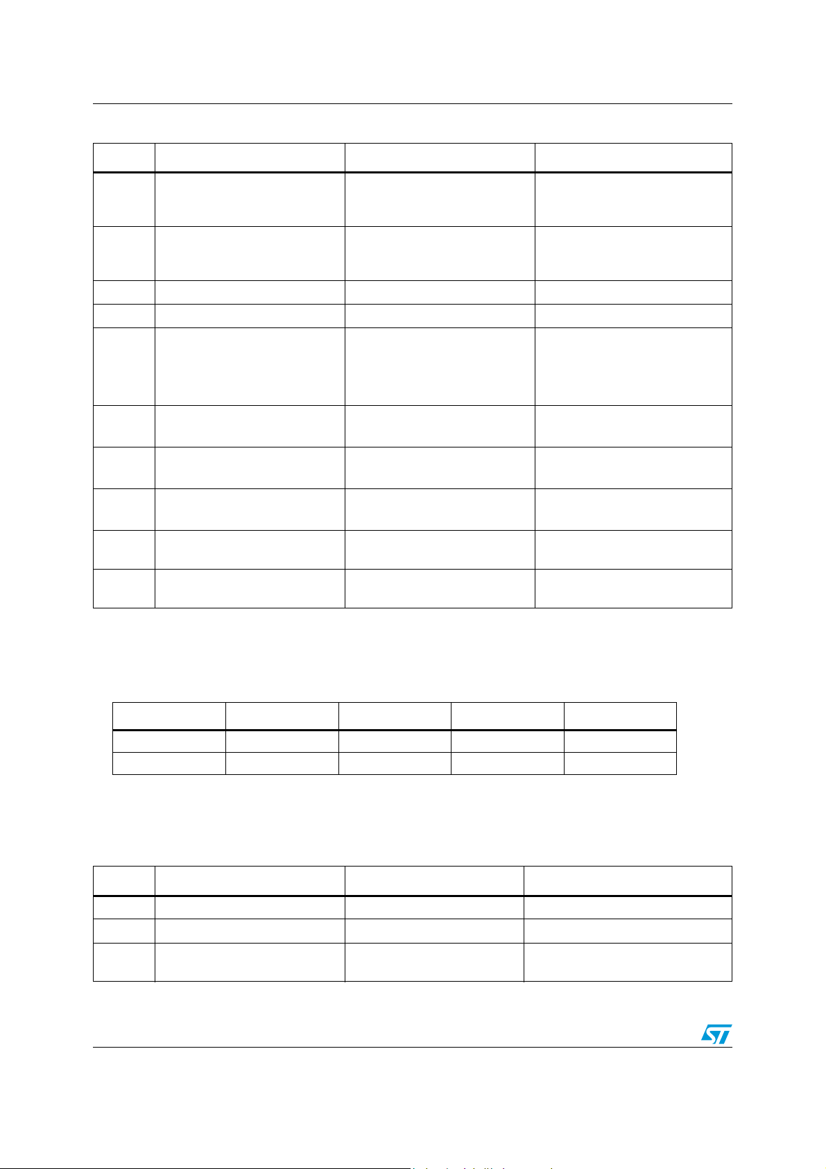
Table 10. External components (continued)
Name Function Formula Typ. value
Positive supply filter capacitor
CVpos
with low impedance for switch
100 μF
mode power supply
Battery supply filter capacitor
CV
with low impedance for switch
100 μF 20% 100 V
mode power supply
CVB High frequency noise filter 470 nF 20% 100 V
(3)
CRD
Q1
D1 DC/DC converter series diode V
RSENSE
RF1
RF2
1. CVpos should be defined depending on the power supply current capability and maximum allowable ripple.
2. For low ripple application use 2 x 47 μF in parallel.
3. Can be saved if proper PCB layout avoid noise coupling on RD pin (high impedance input).
High frequency noise filter 100 nF 10% 15 V
DC/DC converter switch Pchannel MOS transistor
DC/DC converter peak current
limiting
Negative battery programming
level
RDS(ON) ≤ 1.2 Ω,VDS = -100 V
Total gate charge = 20 nC max.
with VGS = 4.5 V and VDS = 1 V
ID > 500 mA
> 100 V, tRR ≤ 50 ns
r
= 100 mV/I
R
SENSE
250 kΩ < RF1 < 300 kΩ
PK
(4)
Possible choiches:
IRF9510 or IRF9520 or
IRF9120 or equivalent
SMBYW01-200
@IPK = 900 mA
@ V
Negative battery programming
leve
l
L DC/DC converter inductor DC resistance ≤ 0.1 Ω
(5)
SUMIDA CDRH125 or equivalent
or equivalent
110 mΩ
300 kΩ 1%
= -70 V
BATR
9.1 kΩ 1%
L=100 μH
(1)
(2)
4 RF1 sets the self generated battery voltage in Ring and Active (Il=0) mode as follows:
267 kΩ 280 kΩ 294 kΩ 300 kΩ
V
BAT(ACTIVE)
V
BATR(RING)
V
should be defined considering the ring peak level required (Vringpeak=V
BATR
provided that the Vpos power supply current capability and the RSENSE programming allow to source all the current
requested by the particular ringer load configuration.
5 For high efficiency in HI-Z mode coil resistance @125 kHz must be < 3 Ω
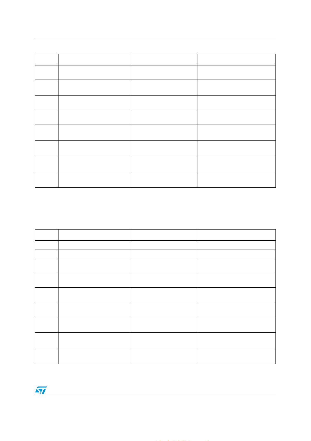
Table 11. External components @gain set = 0
-46 V -48 V -49 V -50 V
-62 V -65 V -68 V -70 V
-6 V typ.). The above relation is valid
BATR
Name Function Formula Typ. value
RS Protection resistance image RS = 50 ⋅ (2Rp) 5 kΩ @ Rp = 50 Ω
ZAC Two wire AC impedance ZAC = 50 ⋅ (Zs - 2Rp) 25 kΩ 1% @ Zs = 600 Ω
ZA
(1)
network
ZA = 50 ⋅ Zs 30 kΩ 1% @ Zs = 600 Ω
SLIC impedance balancing
18/34
Page 19
STLC3055N Application information
Table 11. External components @gain set = 0 (continued)
Name Function Formula Typ. value
Line impedance balancing
(1)
ZB
network
CCOMP AC feedback loop compensation
CH
RTTX
CTTX
Trans-Hybrid Loss frequency
compensation
Pulse metering cancellation
(2)
resistor
Pulse metering cancellation
(2)
capacitor
RLV Pulse metering level resistor
ZB = 50 ⋅ Zl 30 kΩ 1% @ Zl = 600 Ω
fo = 250 kHz
CCOMP = 1/(2π⋅fo⋅100⋅(RP))
120 pF 10% 10 V @ Rp = 50 Ω
CH = CCOMP 120 pF 10% 10 V
RTTX = 50Re (Zlttx+2Rp) 15 kΩ @Zlttx = 200 Ω real
CTTX = 1/{50⋅2π⋅fttx[-
lm(Zlttx)]}
RLV = 63.3·10
3·
·α·V
LOTTX
α = (|Zlttx + 2Rp|/|Zlttx|)
100nF 10% 10V
@ Zlttx = 200Ω real
16.2 kΩ @ V
LOTTX
(3)
= 170mVrms
CS
Pulse metering shaping
capacitor
CS = τ/(2⋅RLV)
CFL Pulse metering filter capacitor CFL = 2/(2π⋅fttx⋅RLV)
1. In case Zs=Zl, ZA and ZB can be replaced by two resistors of same value: RA=RB=|Zs|.
2. Defining ZTTX as the impedance of RTTX in series with CTTX, RTTX and CTTX can also be calculated from the following
formula:
ZTTX=50*(Zlttx+2Rp).
3. In this case CTTX is just operating as a DC decoupling capacitor (fp=100 Hz).
Table 12. External components @gain set = 1
100 nF 10% 10V
@ τ = 3.2 ms, RLV = 16.2 kΩ
1.5 nF 10% 10 V
@fttx = 12 kHz RLV = 16.2 kΩ
Name Function Formula Typ. value
RS Protection resistance image RS = 25 ⋅ (2Rp) 2.55 kΩ @ Rp = 50 Ω
ZAC Two wire AC impedance ZAC = 25 ⋅ (Zs - 2Rp) 12.5 kΩ 1% @ Zs = 600 Ω
SLIC impedance balancing
(1)
ZA
ZB
network
Line impedance balancing
(1)
network
CCOMP AC feedback loop compensation
CH
Trans-Hybrid Loss frequency
compensation
ZA = 25 ⋅ Zs 15 kΩ 1% @ Zs = 600 Ω
ZB = 25 ⋅ Zl 15 kΩ 1% @ ZI = 600 Ω
fo = 250kHz
CCOMP = 2/(2π⋅fo⋅100⋅(RP))
220 pF 10% 10VL @ Rp = 50 Ω
CH = CCOMP 220 pF 10% 10 V
RTTX
CTTX
resistor
Pulse metering cancellation
(2)
capacitor
Pulse metering cancellation
(2)
RLV Pulse metering level resistor
RTTX = 25Re (Zlttx+2Rp) 7.5 kΩ @Zlttx = 200 Ω real
(3)
= 340 mVrms
CTTX = 1/25⋅2π⋅fttx⋅[-lm(Zlttx)]
RLV = 31.7·10
3·
·α·V
LOTTX
α = (|Zlttx + 2Rp|/|Zlttx|)
100 nF 10% 10 V
@ Zlttx = 200 Ω real
16.2 kΩ @ V
LOTTX
19/34
Page 20
Application information STLC3055N
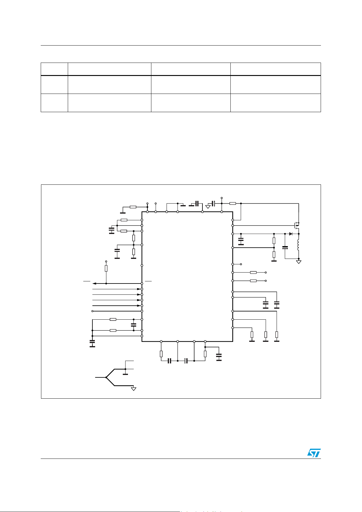
Table 12. External components @gain set = 1 (continued)
Name Function Formula Typ. value
CS
Pulse metering shaping
capacitor
CS = τ/(2⋅RLV)
CFL Pulse metering filter capacitor CFL = 2/(2π⋅fttx⋅RLV)
100 nF 10% 10V
@ τ = 3.2 ms, RLV = 16.2 kΩ
1.5nF 10% 10 V
@fttx = 12 kHz RLV = 16.2 kΩ
1. In case Zs=Zl, ZA and ZB can be replaced by two resistors of same value: RA=RB=|Zs|.
2. Defining ZTTX as the impedance of RTTX in series with CTTX, RTTX and CTTX can also be calculated from the following
formula:
ZTTX=50*(Zlttx+2Rp).
3. In this case CTTX is just operating as a DC decoupling capacitor (fp=100 Hz).
5.3 Application diagram
Figure 8. Application diagram with metering pulse generation.
RD
CVPOS
VPOS
VPOS
RSENSE
GATE
VBAT
CLK
TIP
RING
CSVR
CREV
RTH
RLIM
IREF
RSENSE
VF
CLK
RREF
CVB
RP
RP
CREV
RLIM
TIP
RING
RF1
RF2
CSVR
RTH
Q1
P-ch
D1
L
CV
CONTROL
INTERFACE
TTX CLOCK
DET
D0
D1
D2
PD
CCOMP
CFL
VDD
CH
RDD
RLV
RLV
RS
ZAC
TX
RX
RRX
AGND
TX
RX
RS
ZAC
ZAC1
ZA
ZB
ZB
GAIN SET
BGND
CVCC
CVCC
STLC3055N
DET
D0
D1
D2
PD
CKTTX
CS
CTTX1
CTTX2
FTTX
RTTX
CAC
ILTF
RTTX
SYSTEM GND
SUGGESTED GROUND LAY-OUT
AGND
BGND
PGND
CTTX
20/34
CAC
RD
CRD
D00TL489A
Page 21
STLC3055N Application information
Figure 9. Application diagram without metering pulse generation
CCOMP
CONTROL
INTERFACE
SUGGESTED GROUND LAY-OUT
DET
D0
D1
D2
PD
SYSTEM GND
VDD
CH
RDD
RS
ZAC
RD
CVPOS
RD
VPOS
VPOS
RSENSE
GATE
VBAT
CLK
TIP
RING
CSVR
CREV
RTH
RLIM
IREF
CRD
RSENSE
VF
CLK
RREF
CVB
RP
RP
CREV
RLIM
TIP
RING
D00TL490/B
RF1
RF2
CSVR
RTH
Q1
P-ch
D1
L
CV
TX
RX
RRX
AGND
TX
RX
RS
ZAC
ZAC1
ZA
ZB
ZB
GAIN SET
BGND
CVCC
CVCC
STLC3055N
DET
D0
D1
D2
PD
CKTTX
CTTX1
CTTX2
FTTX
AGND
BGND
PGND
RTTX
CAC
ILTF
CAC
21/34
Page 22
Electrical characteristics STLC3055N
6 Electrical characteristics
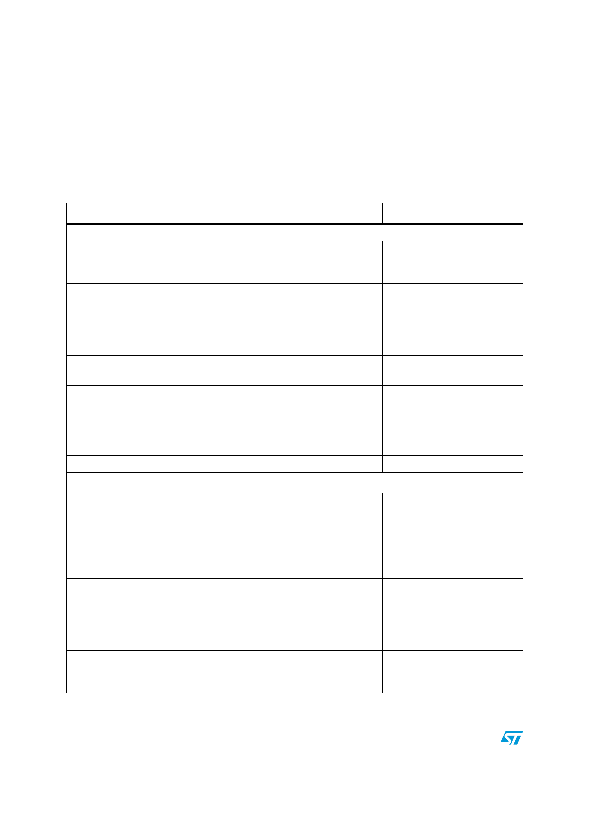
Table 13. Electrical characteristics
Test conditions: V
= 6.0V, AGND = BGND, normal polarity, T
pos
= 25 °C.
amb
External components as listed in the "typical values" column of external components table.
Note: Testing of all parameter is performed at 25 °C. Characterisation as well as design
rules used allow correlation of tested performances at other temperatures. All parameters
listed here are met in the operating range: -40 to +85 °C.
Symbol Parameter Test condition Min. Typ. Max. Unit
DC characteristics
Il = 0, HI-Z
V
V
V
V
Ilim
lohi
lohi
loa
loa
Line voltage
Line voltage
Line voltage
Line voltage
Lim. current programming
range
Ilima Lim. current accuracy
(High impedance feeding)
= 0 to 85 °C
T
amb
Il = 0, HI-Z
(High impedance feeding)
= -40 to 85 °C
T
amb
Il = 0, ACTIVE
T
= 0 to 85 °C
amb
Il = 0, ACTIVE
T
= -40 to 85 °C
amb
ACTIVE mode 20 40 mA
ACTIVE mode.
Rel. to programmed value
20 mA to 40 mA
44 50 V
42 48 V
33 40 V
31 37 V
-10 10 %
Rfeed HI Feeding resistance HI-Z (High Impedance feeding) 2.4 3.6 kΩ
AC characteristics
L/T
T/L
T/L
Long. to transv.
(see Section 6.1: Test circuits.)
Transv. to long.
(see Section 6.1: Test circuits.)
Transv. to long.
(see Section 6.1: Test circuits.)
2WRL 2W return loss
Rp = 50 Ω, 1% tol.,
ACTIVE N. P., R
L
f = 300 to 3400 Hz
Rp = 50 Ω, 1% tol.,
ACTIVE N. P., R
L
f = 300 to 3400 Hz
Rp = 50 Ω, 1% tol.,
ACTIVE N. P., R
L
f = 1 kHz
300 to 3400 Hz,
ACTIVE N. P., R
L
= 600 Ω
= 600 Ω
= 600 Ω
= 600 Ω
(1)
(1)
(1)
(1)
50 58 dB
40 45 dB
48 53 dB
22 26 dB
300 to 3400 Hz,
THL Trans-hybrid loss
20Log|VRX/VTX|,
ACTIVE N. P., RL = 600 Ω
(1)
30 dB
22/34
Page 23
STLC3055N Electrical characteristics
Table 13. Electrical characteristics (continued)
Test conditions: V
= 6.0V, AGND = BGND, normal polarity, T
pos
= 25 °C.
amb
External components as listed in the "typical values" column of external components table.
Note: Testing of all parameter is performed at 25 °C. Characterisation as well as design
rules used allow correlation of tested performances at other temperatures. All parameters
listed here are met in the operating range: -40 to +85 °C.
Symbol Parameter Test condition Min. Typ. Max. Unit
Ovl 2W overload level
TXoff TX output offset ACTIVE N. P., R
G24 Transmit gain abs.
G42 Receive gain abs.
at line terminals on ref. imped.
ACTIVE N. P., R
= 600 Ω
L
= 600 Ω
L
(1)
(1)
0dBm @ 1020Hz,
ACTIVE N. P., R
= 600 Ω
L
(1)
0dBm @ 1020Hz,
ACTIVE N. P., R
= 600 Ω
L
(1)
3.2 dBm
-250 250 mV
-6.4 -5.6 dB
-0.4 0.4 dB
rel. 1020Hz; 0 dBm,
G24f TX gain variation vs. freq.
300 to 3400 Hz,
ACTIVE N. P., RL = 600 Ω
(1)
-0.12 0.12 dB
rel. 1020 Hz; 0 dBm,
G24f RX gain variation vs. freq.
V2Wp
V2Wp
V4Wp
V4Wp
Idle channel noise at line 0dB
gainset
Idle channel noise at line 0dB
gainset
Idle channel noise at line 0dB
gainset
Idle channel noise at line 0dB
gainset
Thd Total Harmonic Distortion ACTIVE N. P., R
VTTX Metering pulse level on line
300 to 3400 Hz,
ACTIVE N. P., RL = 600 Ω
psophometric filtered
ACTIVE N. P., RL = 600 Ω
T
= 0 to +85 °C
amb
psophometric filtered
ACTIVE N. P., R
T
= -40 to +85 °C
amb
= 600 Ω
L
psophometric filtered
ACTIVE N. P., R
T
= 0 to +85 °C
amb
= 600 Ω
L
psophometric filtered
ACTIVE N. P., R
T
= -40 to +85 °C
amb
= 600 Ω
L
= 600 Ω
L
ACTIVE - TTX; Gain Set = 1
Zl = 200 Ω fttx = 12 kHz;
(1)
(1)
(1)
(1)
(1)
(1)
-0.12 0.12 dB
-73 -68 dBmp
-68 dBmp
-75 -70 dBmp
-75 dBmp
-44 dB
260 340 mVrms
CLKfreq CLK operating range -10% 125 10% kHz
Ring
Vring Line voltage
RING D2 toggling @ fr = 25 Hz
Load = 3REN;
Crest Factor = 1.25
1REN = 1800 Ω + 1.0 μF
T
= 0 to +85°C
amb
23/34
45 49 Vrms
Page 24
Electrical characteristics STLC3055N
Table 13. Electrical characteristics (continued)
Test conditions: V
= 6.0V, AGND = BGND, normal polarity, T
pos
= 25 °C.
amb
External components as listed in the "typical values" column of external components table.
Note: Testing of all parameter is performed at 25 °C. Characterisation as well as design
rules used allow correlation of tested performances at other temperatures. All parameters
listed here are met in the operating range: -40 to +85 °C.
Symbol Parameter Test condition Min. Typ. Max. Unit
RING D2 toggling @ fr = 25Hz
Load = 3REN;
Vring Line voltage
Detectors
Crest Factor = 1.25
1REN = 1800Ω + 1.0μF
= -40 to +85°C
T
amb
44 48 Vrms
IOFFTHA Off/hook current threshold
ROFTHA
IONTHA On/hook current threshold
RONTHA
IOFFTHI Off/hook current threshold
ROFFTHI
IONTHI On/hook current threshold
RONTHI
Irt
Irta
Trtd Ring trip detection time Ring mode 60 ms
Td Dialling distortion Active mode -1 1 ms
Rlrt
ThAl Tj for th. alarm activation 160 °C
Off/hook loop resistance
threshold
On/hook loop resistance
threshold
Off/hook loop resistance
threshold
On/hook loop resistance
threshold
Ring Trip detector threshold
range
Ring Trip detector threshold
accuracy
(2)
Loop resistance 500 Ω
ACT. mode, RTH = 32.4kΩ 1%
(Prog. ITH = 9mA)
ACT. mode, RTH = 32.4kΩ 1%
(Prog. ITH = 9mA)
ACT. mode, RTH = 32.4kΩ 1%
(Prog. ITH = 9mA)
ACT. mode, RTH = 32.4kΩ 1%
(Prog. ITH = 9mA)
Hi Z mode, RTH = 32.4kΩ 1%
(Prog. ITH = 9mA)
Hi Z mode, RTH = 32.4kΩ 1%
(Prog. ITH = 9mA)
Hi Z mode, RTH = 32.4kΩ 1%
(Prog. ITH = 9mA)
Hi Z mode, RTH = 32.4kΩ 1%
(Prog. ITH = 9mA)
Ring mode 20 50 mA
Ring mode -15 15 %
10.5 mA
3.4 kΩ
6mA
8kΩ
10.5 mA
800 Ω
6mA
8kΩ
24/34
Page 25
STLC3055N Electrical characteristics
Table 13. Electrical characteristics (continued)
Test conditions: V
= 6.0V, AGND = BGND, normal polarity, T
pos
= 25 °C.
amb
External components as listed in the "typical values" column of external components table.
Note: Testing of all parameter is performed at 25 °C. Characterisation as well as design
rules used allow correlation of tested performances at other temperatures. All parameters
listed here are met in the operating range: -40 to +85 °C.
Symbol Parameter Test condition Min. Typ. Max. Unit
Digital interface
INPUTS: D0, D1, D2, PD, CLK
OUTPUTS: DET
Vih In put high voltage 2 V
Vil Input low voltage 0.8 V
Iih Input high current -10 10 μA
Iil Input low current -10 10 μA
Vol Output low voltage Iol = 1mA 0.45 V
PSRR and power consumption
PSERRC
Ivpos Vpos supply current @ ii = 0
Ipk Peak current limiting accuracy
1. RL: Line Resistance
2. Rlrt = Maximum loop resistance (incl. telephone) for correct ring trip detection.
Power supply rejection Vpos to
2W port
Vripple = 100mVrms
50 to 4000Hz
HI-Z On-Hook
ACTIVE On-Hook,
RING (line open)
RING Off-Hook
RSENSE = 110mΩ
26 36 dB
13
50
55
-20% 950 +20% mApk
25
80
90
mA
mA
mA
25/34
Page 26
Electrical characteristics STLC3055N
6.1 Test circuits
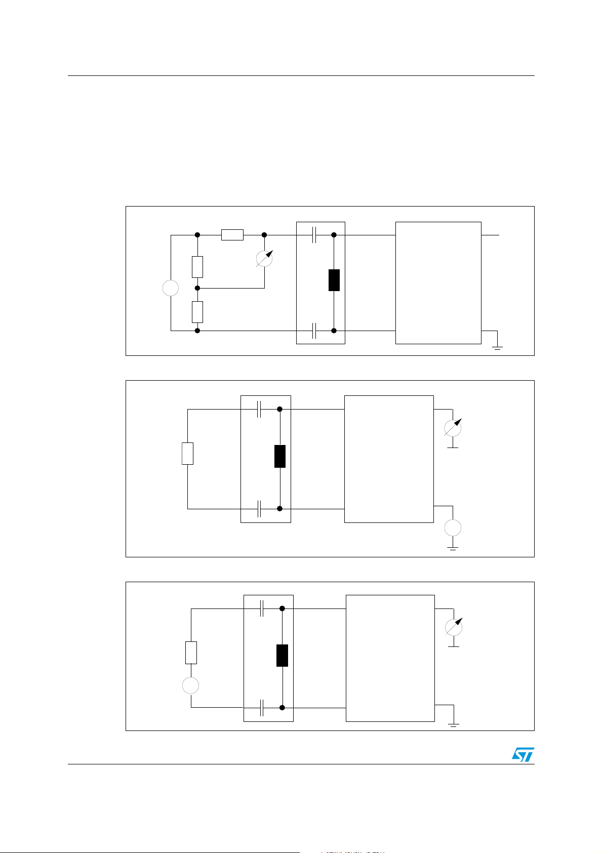
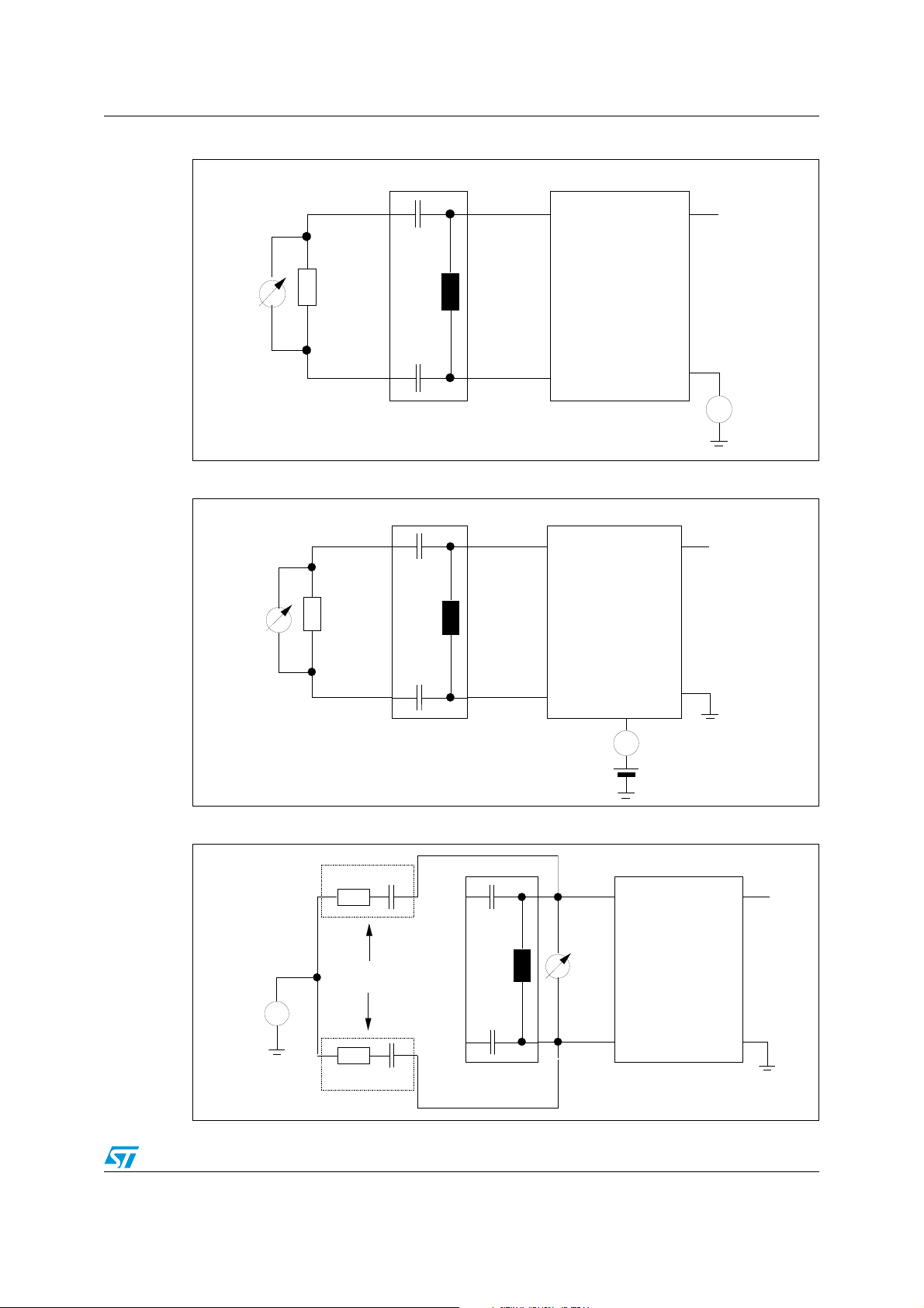
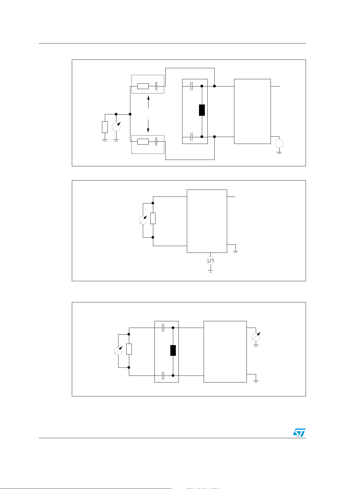
Referring to the application diagram shown in Figure 8 on page 20 and using as external
components the typical values specified in the Table 10 on page 17 and Table 11 on
page 18, find below the proper configuration for each measurement.
All measurements requiring DC current termination should be performed using "Wandel &
Goltermann DC Loop Holding Circuit GH-1" or equivalent.
Figure 10. 2W return loss 2WRL = 20Log(|Zref + Zs|/|Zref-Zs|) = 20Log(E/2Vs)
Vs
W&G GH1
100μF
100mA
DC max
Zin = 100K
200 to 6kHz
100μF
TIP
STLC3055N
application
circuit
RING
TX
RX
Zref
600ohm
1Kohm
E
1Kohm
Figure 11. THL trans hybrid loss THL = 20Log|Vrx/Vtx|
W&G GH1
TIP
100μF
STLC3055N
application
circuit
RING
600ohm
100mA
DC max
Zin = 100K
200 to 6kHz
100μF
Figure 12. G24 transmit gain G24 = 20Log|2Vtx/E|
W&G GH1
TIP
100μF
STLC3055N
application
circuit
RING
600ohm
E
100mA
DC max
Zin = 100K
200 to 6kHz
100μF
TX
Vtx
RX
Vrx
TX
Vtx
RX
26/34
Page 27
STLC3055N Electrical characteristics
Figure 13. G42 receive gain G42 = 20Log|VI/Vrx|
W&G GH1
TIP
100μF
Vl
600ohm
100mA
DC max
Zin = 100K
200 to 6kHz
100μF
STLC3055N
application
circuit
RING
TX
RX
Vrx
Figure 14. PSRRC power supply rejection Vpos to 2W port PSSRC = 20Log|Vn/Vl|
W&G GH1
TIP
100μF
Vl
600ohm
100mA
DC max
Zin = 100K
200 to 6kHz
STLC3055N
application
circuit
TX
100μF
~
RX
Vn
RING
VPOS
Figure 15. L/T longitudinal to transversal conversion L/T = 20Log|Vcm/Vl|
W&G GH1
100μF
100mA
DC max
Zin = 100K
200 to 6kHz
100μF
TIP
STLC3055N
Vl
application
circuit
RING
RX
Vcm
300ohm
300ohm
100μF
Impedance matching
better than 0.1%
100μF
TX
27/34
Page 28
Electrical characteristics STLC3055N
Figure 16. T/L transversal to longitudinal conversion T/L = 20Log|Vrx/Vcm|
W&G GH1
100μF
100mA
DC max
Zin = 100K
200 to 6kHz
100μF
600ohm
Vcm
300ohm
300ohm
100μF
Impedance matching
better than 0.1%
100μF
Figure 17. VTTX metering pulse level on line
TIP
Vlttx
200ohm
STLC3055N
application
circuit
TIP
TX
STLC3055N
application
circuit
RING
TX
RX
Vrx
CKTTX
fttx (12 or 16kHz)
RX
RING
Figure 18. V2Wp and W4Wp: idle channel psophometric noise at line and TX.
V2Wp = 20Log|Vl/0.774l|; V4Wp = 20Log|Vtx/0.774l|
W&G GH1
Vl
psophometric
filtered
600ohm
100μF
100mA
DC max
Zin = 100K
200 to 6kHz
100μF
TIP
STLC3055N
application
circuit
RING
TX
Vtx
psophometric
filtered
RX
28/34
Page 29
STLC3055N Overvoltage protection
7 Overvoltage protection
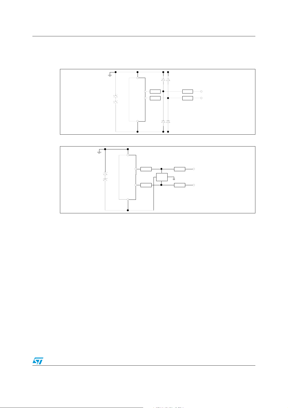
Figure 19. Simplified configuration for indoor overvoltage protection
BGND
STLC3055N
2 x
SM6T39A
RING
VBAT
RP1
TIP
RP1
STPR120A
RP2
RP2
STPR120A
RP1 = 30ohm:
RP2 =Fuse or PTC > 18ohm
TIP
RING
Figure 20. Standard overvoltage protection configuration for K20 compliance
BGND
STLC3055N
RP1
TIP
RP1
LCP1521
RP1 = 30ohm:
RP2 =Fuse or PTC > 18o hm
2 x
SM6T39A
RING
VBAT
RP2
RP2
TIP
RING
29/34
Page 30
Typical state diagram for STLC3055N operation STLC3055N
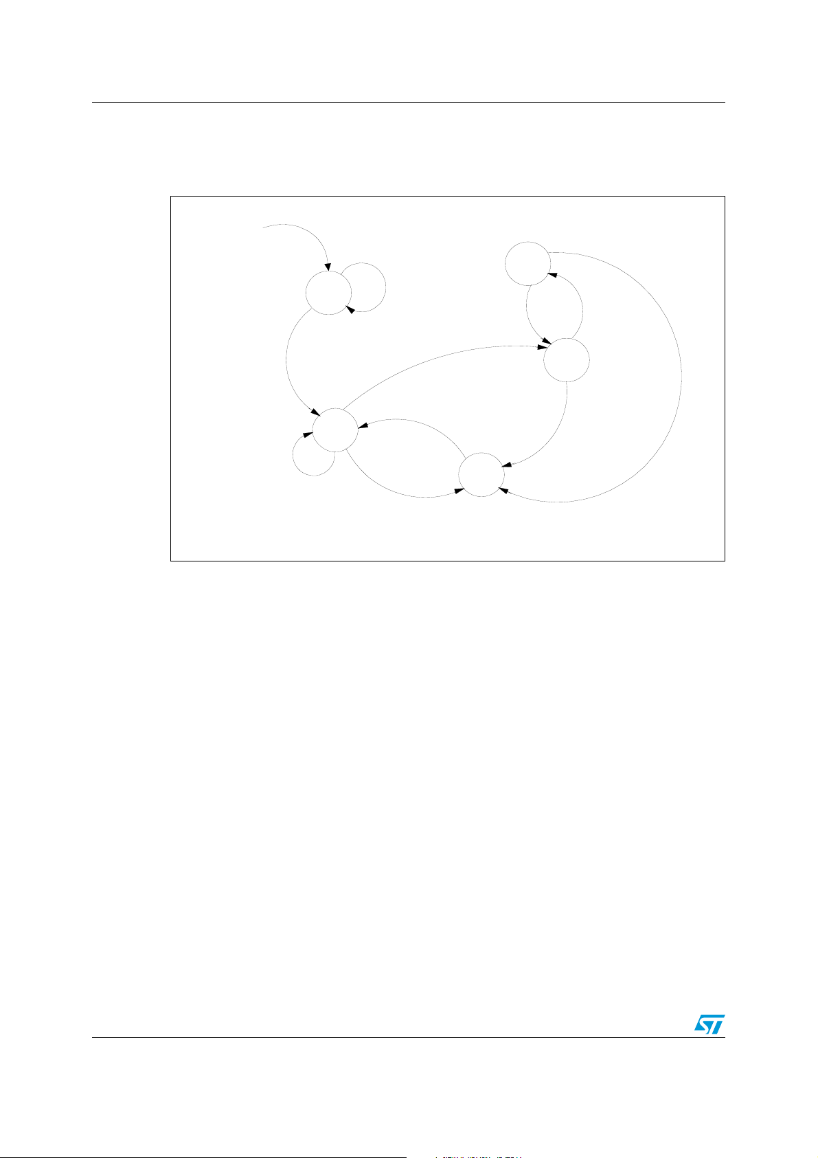
8 Typical state diagram for STLC3055N operation
Figure 21. State diagram
Normally used for
On Hook Transmission
Tj>Tth
PD=1,
D0=D1=0
On Hook Condition
Power
Down
HI-Z
Feeding
PD=0, D0=D1=0
Ring Burst
D0=1, D1=0,
D2=0/1
On Hook Detection for T>Tref
Active
Off Hook
Active
On Hook
Ring Burst
Ring Pause
D0=0, D1=1,
D2=0
Ringing
Ring Trip
Detection
Off Hook Detection
Note: all state tran sitions are under the microprocessor control.
D0=0, D1=1,
D2=0
Off Hook Dete ction
30/34
Page 31
STLC3055N STLC3055Q vs STLC3055N compatibility.
9 STLC3055Q vs STLC3055N compatibility.
STLC3055N is pin to pin compatible with the old STLC3055Q but offer a better performance
in term of power consumption and can be set in a new gain configuration in order to be
compatible with the 3.3 V codec.
9.1 Typical power consumption comparison
Table 14. Power consumption differences
Operative mode STLC3055Q STLC3055N
HI-Z 52 - 60 mA 13 - 25 mA
Active on hook 93 - 115 mA 50 - 80 mA
Ring (no REN) 120 - 140 mA 55 - 90 mA
To meet this result some differences, with a minimum impact on the application, has been
introduced in STLC3055N.
9.2 Hardware differences
● RX input. In STLC3055N it is necessary a 100 kΩ external resistor between RX input
and AGND to bias the input stage.
● Rp. The STLC3055N required a Rp value of 50 Ω instead of 41 Ω.
● TTX filter. To optimize the ttx signal dynamic, the values of RLV and CFL have been
changed;
Table 15. Hardware differences
Component STLC3055Q STLC3055N
RRX 100 kΩ
Rp 41 Ω 50 Ω
RLV 27 kΩ 16.2 kΩ
CFL 1 nF 1.5 nF
9.3 Parameter differences
Table 16. Parameter differences
Parameter STLC3055Q STLC3055N
Absolute max. rating 17 V 13 V
Operating range 15.8 V 12 V
Typ. metering pulse level (Gs 1) 340 mVrms
Typ. metering pulse level (Gs 0) 200 mV
31/34
rms
170 mV
rms
Page 32
Package information STLC3055N
10 Package information
In order to meet environmental requirements, ST offers these devices in different grades of
ECOPACK
®
packages, depending on their level of environmental compliance. ECOPACK
®
specifications, grade definitions and product status are available at: www.st.com.
ECOPACK
®
is an ST trademark.
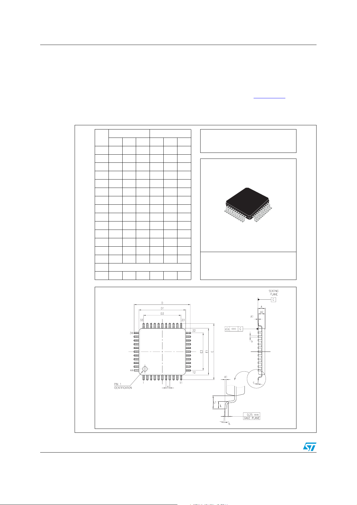
Figure 22. LQFP44 (10 x 10 x 1.4 mm) mechanical data and package dimensions
DIM.
A 1.60 0.063
A1 0.05 0.15 0.002 0.006
A2 1.35 1.40 1.45 0.053 0.055 0.057
B 0.30 0.37 0.45 0.012 0.015 0.018
C 0.09 0.20 0.004 0.008
D 11.80 12.00 12.20 0.464 0.472 0.480
D1 9.80 10.00 10.20 0.386 0.394 0.401
D3 8.00 0.315
E 11.80 12.00 12.20 0.464 0.472 0.480
E1 9.80 10.00 10.20 0.386 0.394 0.401
E3 8.00 0.315
e0.80 0.031
L 0.45 0.60 0.75 0.018 0.024 0.030
L1 1.00 0.039
k 0˚(min.), 3.5˚(typ.), 7˚(max.)
ccc 0.10 0.0039
mm inch
MIN. TYP. MAX. MIN. TYP. MAX.
OUTLINE AND
MECHANICAL DATA
LQFP44 (10 x 10 x 1.4mm)
32/34
0076922 E
Page 33
STLC3055N Revision history
11 Revision history
Table 17. Document revision history
Date Revision Changes
11-Sep-2003 4 First Issue
Update Functional Description and Electrical Characteristics.
01-Oct-2004 5
15-Oct-2004 6 Modified the application diagrams and some typo errors.
05-Nov-2004 7
Aligned the graphic style to be compliant with the new “Corporate
Technical Publications Design Guide”
Removed all max. values of the ‘Line Voltage’ parameter on the page
14/24.
Changed the unit from mA to % of the ‘Ilima’ parameter on the page
14/24.
15-Jan-2005 8
01-Jul-2005 9 Changed VTTX value
21-Feb-2006 10
12-Feb-2009 11
Add pin 4 PD in Applications and Block Diagram
Add in Table 2 ‘ESD Rating’
Added part number “E-STLC3055N” (ECOPACK).
Added RRX resistance in the figures 9 and 10.
Added Appendix D.
Document reformatted.
Updated Section 10: Package information on page 32.
33/34
Page 34

STLC3055N
Please Read Carefully:
Information in this document is provided solely in connection with ST products. STMicroelectronics NV and its subsidiaries (“ST”) reserve the
right to make changes, corrections, modifications or improvements, to this document, and the products and services described herein at any
time, without notice.
All ST products are sold pursuant to ST’s terms and conditions of sale.
Purchasers are solely responsible for the choice, selection and use of the ST products and services described herein, and ST assumes no
liability whatsoever relating to the choice, selection or use of the ST products and services described herein.
No license, express or implied, by estoppel or otherwise, to any intellectual property rights is granted under this document. If any part of this
document refers to any third party products or services it shall not be deemed a license grant by ST for the use of such third party products
or services, or any intellectual property contained therein or considered as a warranty covering the use in any manner whatsoever of such
third party products or services or any intellectual property contained therein.
UNLESS OTHERWISE SET FORTH IN ST’S TERMS AND CONDITIONS OF SALE ST DISCLAIMS ANY EXPRESS OR IMPLIED
WARRANTY WITH RESPECT TO THE USE AND/OR SALE OF ST PRODUCTS INCLUDING WITHOUT LIMITATION IMPLIED
WARRANTIES OF MERCHANTABILITY, FITNESS FOR A PARTICULAR PURPOSE (AND THEIR EQUIVALENTS UNDER THE LAWS
OF ANY JURISDICTION), OR INFRINGEMENT OF ANY PATENT, COPYRIGHT OR OTHER INTELLECTUAL PROPERTY RIGHT.
UNLESS EXPRESSLY APPROVED IN WRITING BY AN AUTHORIZED ST REPRESENTATIVE, ST PRODUCTS ARE NOT
RECOMMENDED, AUTHORIZED OR WARRANTED FOR USE IN MILITARY, AIR CRAFT, SPACE, LIFE SAVING, OR LIFE SUSTAINING
APPLICATIONS, NOR IN PRODUCTS OR SYSTEMS WHERE FAILURE OR MALFUNCTION MAY RESULT IN PERSONAL INJURY,
DEATH, OR SEVERE PROPERTY OR ENVIRONMENTAL DAMAGE. ST PRODUCTS WHICH ARE NOT SPECIFIED AS "AUTOMOTIVE
GRADE" MAY ONLY BE USED IN AUTOMOTIVE APPLICATIONS AT USER’S OWN RISK.
Resale of ST products with provisions different from the statements and/or technical features set forth in this document shall immediately void
any warranty granted by ST for the ST product or service described herein and shall not create or extend in any manner whatsoever, any
liability of ST.
ST and the ST logo are trademarks or registered trademarks of ST in various countries.
Information in this document supersedes and replaces all information previously supplied.
The ST logo is a registered trademark of STMicroelectronics. All other names are the property of their respective owners.
© 2009 STMicroelectronics - All rights reserved
STMicroelectronics group of companies
Australia - Belgium - Brazil - Canada - China - Czech Republic - Finland - France - Germany - Hong Kong - India - Israel - Italy - Japan -
Malaysia - Malta - Morocco - Singapore - Spain - Sweden - Switzerland - United Kingdom - United States of America
www.st.com
34/34
 Loading...