

STLC2150
BLUETOOTH® RADIO TRANSCEIVER
■ Bluetooth
■ Fully integrated single chip:
®
v.1.2 specification compliant
– transceiver with minimum of external RF
components
– PLL completely integrated
– Integrated antenna switch
■ Supports Power Class 2 and 3 operation with
power control
■ Supports Power Class 1 operation with an
external Power Amplifie
■ Outstanding maximum usable input signal
■ Interface with base-band:
– BlueRF compatible
– unidirectional
– received data: RxMode2 and RxMode2+ are
supported
– serial interface: JTAG
■ CMOS technology
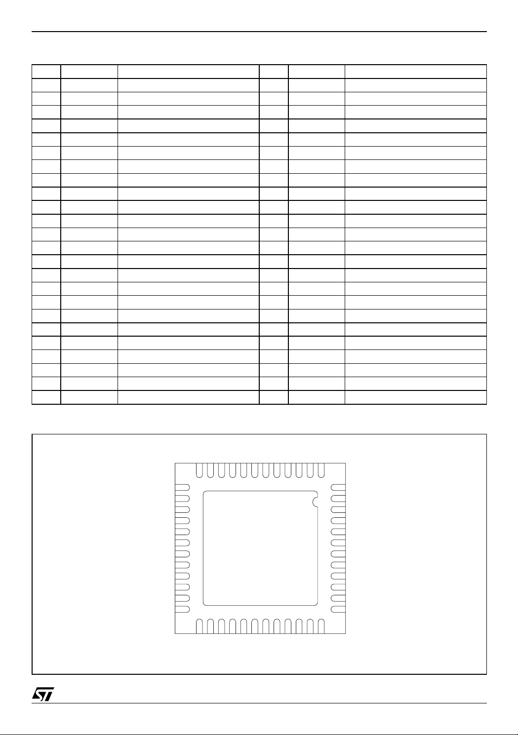
■ Standard VFQFPN-48 package
■ Low standby power consumption
■ Extended temperature range
■
Compliant to automotive specification AEC-Q100
APPLICATIONS
■
Wireless data transmission applications to 432
Kbps symmetrical or 721 Kbps asymmetrical.
■
Typical applications in which the STLC2150 is
used are:
■
Computer peripherals
■
Modems
■
Cameras
■
Portable computers, PDA
■
Handheld data transfer devices
■
Mobile phone
■
Other types of devices that require the wireless
communication provided by Bluetooth
®
.
VFQFPN-48 (7x7x1.0mm)
ORDERING NUMBER: STLC2150
Temperature range: -40 to 85 °C
DESCRIPTION
The STLC2150 is a fully integrated
Bluetooth® single
chip radio transceiver. Together with a BB processor,
like STLC2410, it offers a compact and complete solution for short-range wireless connectivity for a variety of applications.
The STLC2150 implements a low-IF receiver for
Bluetooth® modulated input signals and no external
IF filtering is required. The GFSK demodulator is fully
integrated and supplies digital output data and RSSI.
The transmit section features a fully integrated GFSK
modulator, followed by a direct up-conversion stage,
giving an output signal of 0 dBm. Optional power control is available.
On-chip VCO covers full
Bluetooth® band and contains all of the tank resonator circuitry. Unidirectional
BlueRF compatible interface and 4 wires serial JTAG
interface are used to control all functions of radio
transceiver, enabling operation with wide range of BB
processors.
January 2004
Rev. 2.0
1/10
STLC2150
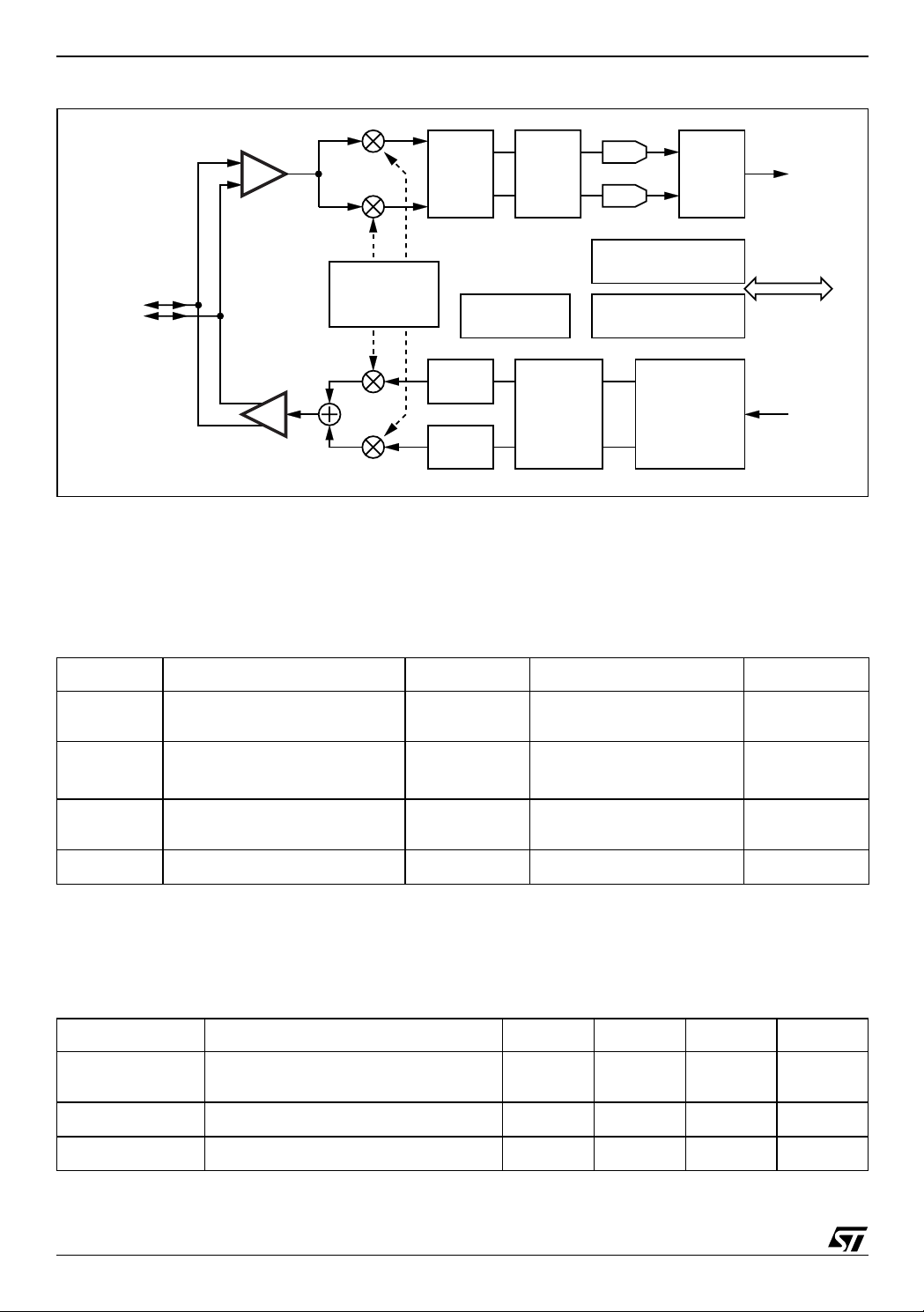
BLOCK DIAGRAM
LNA
MIX
IQ-
BPF
A/D
VGA
A/D
RX
DIGITAL
PA RT
BRXD
POWER & CLOCK
ANTENNA
PLL
& VCO
FILTER
CALIBRATION
CONTROL
SERIAL PROGRAM
INTERFACE
BLUE RF
LPF
PA
MIX
DAC
SYSTEM
MODULATOR
BTXD
LPF
QUICK REFERENCE DATA
Table 1. Absolute Maximum Ratings
Operation of the device beyond these conditions is not guaranteed.
Sustained exposure to these limits will adversely effect device reliability.
Symbol Conditions Min Max Unit
D02TL547
V
DD
Power supply Analogue and
VSS - 0.3 3.5 V
Digital Core
V
SSDIF
V
IN
Input voltage on any pin VSS - 0.3
Maximum voltage difference
-0.3 0.3 V
+ 0.3 AND < 3.5
V
DD
V
+ 0.3 AND < 4.6
DDIO
(*)
V
between different VSS* pins
V
DDIO
(*) Analogue test and RF pins only.
Power supply for digital I/O V
- 0.3 4.6 V
SS
Table 2. Operating Ranges
Operating ranges define the limits for functional operation and parametric characteristics of the device. Functionality outside these limits is not implied.
Symbol Conditions Min Typ Max Unit
V
V
T
DD
DDIO
amb
Power supply Analogue and Digital
2.62 2.70 2.78 V
Core
Power supply for I/O 2.50 3.60 V
Ambient temperature -40 85 °C
2/10
STLC2150
Pin Description and Assignment
Pin# Pin Name Description Pin# Pin Name Description
1 VSS3 Analogue Ground 25 XTAL130
2 AOUTIP Analogue test output 26 XTAL13I 13 MHz Crystal oscillator input pin
3 AOUTIN Analogue test output 27 VDDXTAL 13 MHz oscillator supply
4 AOUTQP Analogue test output 28 VSS1 Analogue Ground
5 AOUTQN Analogue test output 29 VDD1 Analogue Supply
6 LPCLK 3.2 or 32 KHz clock output 30 VDD2 Analogue Supply
7 BDCLK JTAG TCK 31 VSS2 Analogue Ground
8 DVDD1 Digital Core Supply pin 32 VSS6 Analogue Ground
9 DVSS1 Digital Core Ground pin 33 VDD6 Analogue Supply
10 BNDEN JTAG TMS 34 VDD5 Analogue Supply
11 BMOSI JTAG TDI 35 VSS5 Analogue Ground
12 BMISO JTAG TDO 36 VDD7 Analogue Supply
13 RESETN Reset 37 VSS7 Analogue Ground
14 BXTLEN Oscillator enable 38 AINQN Analogue test input
15 BTXEN Tx path enable 39 AINQP Analogue test input
16 BRXEN Rx path enable 40 VDD4 Analogue Supply
17 IOVDD1 Digital IO Supply pin 41 VSS4 Analogue Ground
18 CLK13MHZ 13 MHz output 42 RF_N RF antenna connection
19 BTXD Tx data 43 RF_P RF antenna connection
20 BRCLK 1 MHz-clock associated with data 44 VSS4 Analogue Ground
21 OTP_ZAP OTP ZAP 45 VDD4 Analogue Supply
22 BPKTCTL
Access code successfully decoded
46 AININ Analogue test input
23 BRXD Rx data 47 AINIP Analogue test input
24 BSEN Synthesizer enable 48 VDD3 Analogue Supply
13 MHz Crystal oscillator output pin
PIN CONNECTION
(bottom view)
VDD7
VSS5
VDD5
VDD6
VSS6
VSS2
VDD2
VDD1
VSS1
VDDXTAL
XTAL13I
XTAL13O
VSS7
AINQN
AINQP
VDD4
VSS4
RF_N
RF_P
VSS4
VDD4
AININ
37 38 39 40 41 42 43 44 45 46 47 48
36
35
34
33
32
31
30
29
28
27
26
25
24 23 22 21 20 19 18 17 16 15 14 13
BSEN
BRXD
BPKTCTL
BRCLK
OTP_ZAP
BTXD
CLK13MHZ
IOVDD1
BTXEN
BRXEN
AINIP
VDD3
1 VSS3
2
3
4
5
6
7
8
9
10
11
12
BXTLEN
RESETN
AOUTIP
AOUTIN
AOUTQP
AOUTQN
LPCLK
BDCLK
DVDD1
DVSS1
BNDEN
BMOSI
BMISO
3/10

STLC2150
CURRENT CONSUMPTION
Table 3. Typical Current Consumption
Symbol Parameter Typ Max Unit
Istby Current consumption in standby mode (@27 °C) 5 µA
Irx Current consumption in Receive mode 40 52 mA
Itx Current consumption in Transmit mode 66 80 mA
Ivco Current consumption when only PLL is enabled 22 TBD mA
I32K Current consumption when only the 32-kHz clock oscillator is operating TBD TBD µA
I/O CELL CHARACTERISTICS
Table 4: CMOS DC Electrical characteristics, rated for the operating range
Symbol Parameter Min Max Unit
V
V
V
V
V
V
High Level Input Voltage 80% of V
IH
Low Level Input Voltage 20% of V
IL
High Level Output Voltage 85% of V
OH
Low Level Output Voltage 0.4 V
OL
Schmitt trigger rising threshold 1.4 2.0 V
t+
Schmitt trigger falling threshold 0.5 1.2 V
t-
DDIO
DDIO
Schmitt trigger minimum hysteresis 248 mV
DDIO
V
V
V
APPLICATION REFERENCE DESIGN
Figure 1. reference design schematic diagram
bdclk
bmosi
bmiso
sys_clk_req
brxen
2.7V
C1
100nF
btxd
brclk
bpkctl
brxd
bsen
LPCLK
BDCLK
BNDENbnden
BMOSI
BMISO
RESETNRESET
BXTLEN
BTXENbtxen
BRXEN
IOVDD
OTP_ZAP
CLK13MHZxin
BTXD
BRCLK
BPKTCTL
BRXD
BSEN
XTAL13O
DVDD DVSS
6
7
10
11
12
13
14
15
16
17
21
18
19
20
22
23
24
25 26 28 31 32 35
XTAL13I
98
2
AOUTIP
VSS3
1
3
AOUTIN
2.7V
C8
100nF
VDD345VDD4
STLC2150STLC2410
4
AOUTQP
48
5
AOUTQN
2.7V
C7
100nF
VDD4
40
VSS1 VSS2 VSS6 VSS5
2.7V
C6
100nF
43
42
47
46
44
41
39
38
37
27
29
30
33
34
36
IMPEDANCE ADAPTATION
+BPF
RF_P
RF_N
AINIP
AININ
VSS4
VSS4
AINQP
AINQN
VSS7
VDDXTL
VDD1
VDD2
VDD6
VDD5
VDD7
C4
100nF
2.7V
50Ω
1
2
4/10
C2
15pF
Y1
13MHz
C3
15pF
D02TL548A

STLC2150
FUNCTIONAL DESCRIPTION
Receiver
The STLC2150 implements a low-IF receiver for
from 75
Ω
balanced RF input and amplified by an LNA.
The mixers are driven by two quadrature signals which are locally generated from a VCO signal running at
twice the frequency. The output signals in the I signal path and Q signal path are bandpass filtered by a
polyphase bandpass filter for channel filtering and image rejection. The output of the lowpass filters is amplified
by a VGA to the optimal input range for the A/D converters.
Further filtering is done in digital filters. The digital part demodulates the GFSK coded bit stream by evaluating
the phase information in the I and Q signals.
The digital part recovers the receive bit clock. It extracts RSSI data by calculating the signal strength. Overall
automatic gain amplification in the receive path is controlled by the digital part.
Transmitter
The transmitter takes the serial input transmit data from the base-band. This data is GFSK modulated to I and
Q signals. The Tx bit clock is provided to the base-band for synchronization.
The output of the digital part is converted to analogue signals which are lowpass filtered before being sent to
direct up-conversion mixers.
The quadrature up-conversion mixers use the same LO as the receiver. 0dBm output power at the antenna port
is achieved with an internal PA, which has 75
Bluetooth® modulated input signals. The radio signal is taken
Ω
balanced RF output. Optional power control is available.
PLL
The on-chip VCO is part of a PLL, the frequency is programmed for the RF channels by the digital part. The tank
resonator circuitry for the VCO is completely integrated.
Process variations on the VCO center frequency are calibrated out automatically. Also the RC time constants
for the analogue lowpass filters are automatically calibrated on chip.
Base-band interface
Unidirectional BlueRF compatible interface is used to control all functions of radio transceiver.
The unidirectional RXMODE2 is supported. STLC2150 has also the capability to provide the recovered clock
and the aligned data to the base-band (Rxmode2+). 4 wires serial JTAG interface is used to access the internal
registers. Also JTAG is used to set channel number and read RSSI.
Crystal oscillator
The STLC2150 has a crystal oscillator to generate 13 MHz reference clock for internal use and for the baseband chip.
Also a 3.2 or 32 kHz clock for low power modes operation can be provided.
5/10

STLC2150
GENERAL SPECIFICATION
All the provided values are specified over the operational conditions (VDD and temperature) according to the
Bluetooth® v.1.2 specification.
Receiver
To comply with the
in the bands: 30MHz - 2000MHz and 3000MHz - 12.75GHz. All specification below are measured at the antenna
port. The loss between IC inputs and the port is approximately 2dB
Symbol Parameter Test condition Min Typ Max Unit
RFin Input frequency range 2402 2480 MHz
RXsens Receiver sensitivity
RXmax Max input signal level @BER 0.1% >16 dBm
Receiver interference Performance @BER 0.1%
C/I
co-channel
C/I
1MHz
C/I
2MHz
C/I
≥3MHz
C/I
image
C/I
image±1MHz
Receiver blocking @BER 0.1%
RXB_1 30 MHz – 2000 MHz
RXB_2 2000 MHz – 2400 MHz
Receiver intermodulation
RXIIP3 Input referred IP3 Interferers at –39 dBm,
1) Sensitivity at chip pins is -79.5 dBm.
2) Guarantied over process variation and full temperature range -40 to +85°C.
3) Without any exception.
Bluetooth® norm, an external RF filter is required to provide minimum 17dB of attenuation
(including dirty signal test)
Co-channel interference
Adjacent (1MHz)
interference
Adjacent (2MHz)
interference
Adjacent (≥3MHz)
interference
Image interference
Adjacent (1MHz) to image
interference
3000 MHz – 12.75 GHz
2500 MHz – 3000 MHz
@BER 0.1%
3)
@ Input signal strength = -60 dBm
@ Input signal strength = -60 dBm
@ Input signal strength = -60 dBm
@ Input signal strength = -67 dBm
@ Input signal strength = -67 dBm
@ Input signal strength = -67 dBm
@ input signal strength = -67 dBm
@ input signal strength = -67dBm
intended channel at –64 dBm,
BER < 0.1%
1)
-77.5
10 11 dB
-1 0 dB
-36 -30 dB
-50 -42 dB
-25 -11 dB
-40 -28 dB
-7.5 -11.5 dBm
2)
-73.7
-10 dBm
-27 dBm
dBm
RSSI Extraction
The RSSI extraction block allows to determine the Received Signal Strength. The indicator output is an 8-bit
word, indicating the signal strength in dBm
Symbol Parameter Test condition / notes Min Typ Max Unit
RSSI_AC RSSI accuracy Signal power = -70 dBm ± 4 dB
RSSI_R RSSI range Range upwards from –70 dBm 20 40 dB
RSSI_RES RSSI Resolution 0.37 dB/bit
RSSI_REF RSSI reference point signal power = -64 dBm 107
The RSSI value is stored in the RSSI register. The value is latched when the base-band sends the access code
recognition signal (BPKTCTL) and is kept unchanged until the next RX active slot. The register can be read by
the base-band at any time
6/10

STLC2150
Transmitter
All output power specifications are given at the antenna port, with a bandpass filter and matching network in
between the port and the IC. The loss between antenna port and IC output is approximately 2 dB
Symbol Parameter Test condition Min Typ Max Unit
RFout Output frequency range
TXPout Nominal output power @ 2402 – 2480 MHz -6 0 +4 dBm
In-band spurious emission
TX_SE1 Frequency offset =
±550kHz
TX_SE2 Channel offset = 2 -51 dBm
TX_SE3 Channel offset ≥ 3 -62 dBm
Out-of-band spurious emission
TX_SE4 Emission in the 30 MHz – 1
GHz band
TX_SE5 Emission in the 1 GHz –
12.75 GHz band
TX_SE6 Emission in the 1.8 GHz –
1.9 GHz band
TX_SE7 Emission in the 5.15 GHz –
5.3 GHz band
Bluetooth
Measured in a 100 kHz
bandwidth
Operation mode -65 dBm
Idle mode -65
Operation mode -58 dBm
Idle mode -65
Operation mode -65 dBm
Idle mode -65
Operation mode -65 dBm
Idle mode -65
®
frequency band
2402 2480 MHz
-26 -20 dBc
PLL
The centre frequency of the radio transmit or receive channel is controlled by a PLL. The selected radio channel
centre frequency is given by:
Fc = 2.400GHz + n*1 MHz,
where "n" is a 7-bit channel control word, ranging from 2 to 97
Symbol Parameter Test condition Min Typ Max Unit
Fref External reference clock -20ppm 13.000 +20ppm MHz
VCOset VCO settling time after
power up
Fd Transmitter frequency drift ±100 Hz/µs
From Channel selection to
LOCK = H
40 100 µs
7/10

STLC2150
Crystal oscillator
An on-chip crystal oscillator provides a 13MHz master clock. The external crystal must be connected to the pads
XTAL13I and XTAL13O.
The frequency specification of ±20 ppm can be achieved by 2 different ways:
1. by external components choice (default);
2. by internal tuning (with internal capacitors as defined by the control word stored in the registers.
The control word allows modifying the value of the capacitor connected to the oscillator pads. The total capacitance (including the parasitic capacitors) must be about 16 pF.
The variable capacitor is implemented as a capacitor array of about 255 x 90 fF.
External crystal example
Parameter Value Unit tolerance Comment
Frequency 13.000000 MHz ± 10 ppm At 25 °C ± 3 °C
Mode Fundamental
Drive level 100 µW± 20
Temp drift ±10 ppm Referred to value at 25°C over temperature
Aging ±1 Ppm/year max
Cload 16.0 pF ± 1 %
Rseries 40 Ω max
C0 1.7 pF ± 20 % Shunt capacitance
C1 6.5 pF ± 24 % Motional capacitance
Rins 500 MΩ min Insulation resistance
Pull_sens 10 Ppm ± 20 % (16 pF)
Activity Dips ± 0.5 Ppm / °C max
1)
Temperaure range is defined by application needs.
1)
range
Temperature range
1)
Low power clock
The STLC2150 can provide 3.2 or 32 KHz, low power clock for baseband chip operation in Hold, Snif and Park
modes.
External reference frequency
The STLC2150 can take a digital clock from external source 13 MHz on the CLK13MHZ pin.
The IC also can use an analogue (sine wave, from 0.2 up to 1 Vpp) clock from external 13 MHz source on the
XTAL13I pin.
Registers description
To provide operational control, configuration flexibility (e.g. clock configuration, XTAL trimming) and to set maximum performance the STLC2150 has a bank of registers. Detailed description is available in “STLC2150: Interface and Programming Guide”.
8/10

mm inch
DIM.
MIN. TYP. MAX. MIN. TYP. MAX.
A 0.800 0.900 1.000 0.031 0.035 0.039
A1 0.020 0.050 0.0008 0.0019
A2 0.650 1.000 0.025 0.039
A3 0.250 0.01
b 0.180 0.230 0.300 0.007 0.009 0.012
D 6.850 7.000 7.150 0.269 0.275 0.281
D2 2.250 4.700 5.250 0.088 0.185 0.207
E 6.850 7.000 7.150 0.269 0.275 0.281
E2 2.250 4.700 5.250 0.088 0.185 0.207
e 0.450 0.500 0.550 0.018 0.020 0.022
STLC2150
OUTLINE AND
MECHANICAL DATA
L 0.300 0.400 0.500 0.012 0.016 0.020
ddd 0.080 0.003
VFQFPN-48 (7x7x1.0mm)
V
ery Fine Quad Flat Package
No
lead
7446345_A
9/10

STLC2150
Information furnished is believed to be accurate and reliable. However, STMicroelectronics assumes no responsibility for the consequences
of use of such information nor for any infringement of patents or other rights of third parties which may result from its use. No license is granted
by implication or otherwise under any patent or patent rights of STMicroelectronics. Specifications mentioned in this publication are subject
to change without notice. This publication supersedes an d replaces all information p reviously supplied. STMicroelectronics products are not
authorized for use as critical components in life support devices or systems without express written approval of STMicroelectronics.
The ST logo is a registered trademark of STMicroelectronics.
The BLUETOOTH® word mark and logos are owned by t he Bluetooth SIG, Inc. and any use of such marks by STMicroelectroni cs is under l icense.
All other names are the property of their respective owners
© 2004 STMicroelectronics - All rights reserved
STMicroelectronics GROUP OF COMPANIES
Australia - Belgium - Brazil - Canada - China - Czech Republic - Finland - France - Germany - Hong Kong - India - Israel - Italy - Japan -
Malaysia - Malta - Morocco - Singapore - Spain - Sweden - Switzerland - United Kingdom - United States
www.st.com
10/10
 Loading...