

White LED driver for display backlight
Features
■ Boost DC-DC converter
■ Drives up to 6 LEDs with a total current up to 20
mA
■ Output power capability up to 500 mW
■ Input voltage range 2.5 V to 18 V
■ Output current control
■ 2.3 MHz switching frequency
■ PWM input for the output current dimming with
300:1 dimming range
■ 350 mA integrated switch
■ Overvoltage protection
■ Chip overtemperature detection and protection
■ Soft-start implemented
■ Package DFN6 2 x 2 mm
STLA02
DFN6 (2 x 2 mm)
on/off by the logic signal connected to the EN pin
and this pin is also dedicated for the PWM
dimming of the output current. Current mode
control of the regulation allows a fast response to
a change of the enable pin voltage level.
Applications
■ PDA and handheld devices
■ Cellular phones
■ MP3 players
Description
STLA02 is a boost converter that operates from
2.5 V to 18 V and can provide an output voltage
as high as 27 V and can drive up to 6 white LEDs
connected in series. The total output current
capability is 20 mA at an output voltage of 24 V.
The total output power capability is up to 500 mW.
The regulation is done by the internal error
amplifier which works with the feedback voltage
from the sensing resistor connected in high side
sensing configuration. The device can be turned
Table 1. Device summary
Part number Order code Package
STLA02 STLA02PUR DFN6 (2 x 2 mm)
February 2011 Doc ID 010005 Rev 1 1/23
www.st.com
23

Contents STLA02
Contents
1 Diagram . . . . . . . . . . . . . . . . . . . . . . . . . . . . . . . . . . . . . . . . . . . . . . . . . . . 3
2 Pin configuration . . . . . . . . . . . . . . . . . . . . . . . . . . . . . . . . . . . . . . . . . . . 4
3 Maximum ratings . . . . . . . . . . . . . . . . . . . . . . . . . . . . . . . . . . . . . . . . . . . . 5
4 Application . . . . . . . . . . . . . . . . . . . . . . . . . . . . . . . . . . . . . . . . . . . . . . . . 6
5 Electrical characteristics . . . . . . . . . . . . . . . . . . . . . . . . . . . . . . . . . . . . . 7
6 Typical performance characteristics . . . . . . . . . . . . . . . . . . . . . . . . . . . . 8
7 Introduction . . . . . . . . . . . . . . . . . . . . . . . . . . . . . . . . . . . . . . . . . . . . . . . 14
7.1 PWM input (EN) . . . . . . . . . . . . . . . . . . . . . . . . . . . . . . . . . . . . . . . . . . . . 14
7.2 Selection of the external components . . . . . . . . . . . . . . . . . . . . . . . . . . . 14
8 Package mechanical data . . . . . . . . . . . . . . . . . . . . . . . . . . . . . . . . . . . . 18
9 Revision history . . . . . . . . . . . . . . . . . . . . . . . . . . . . . . . . . . . . . . . . . . . 22
2/23 Doc ID 010005 Rev 1
STLA02 Diagram
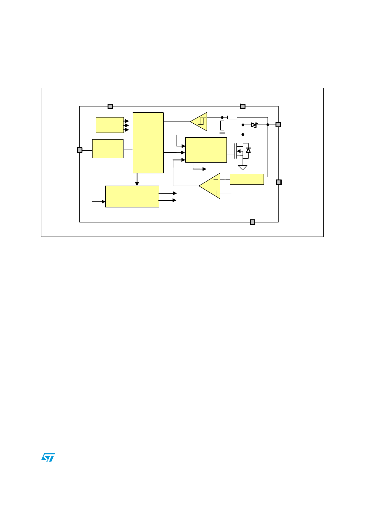
1 Diagram
Figure 1. Block diagram
VIN
EN/
EN/
PWM
PWM
12 V/5 V
12 V/5 V
CONV
CONV
ILIM
ILIM
VIN
BIAS
BIAS
REFERENCE
REFERENCE
LOGIC
LOGIC
VSET
VSET
VBG
VBG
OVP
OVP
VBG
VBG
STEP-UP
STEP-UP
CONTROL
CONTROL
ILIM
ILIM
VLX
VLX
FB SENSING
FB SENSING
VSET
VSET
VOUT
VOUT
FB
FB
GND
GND
AM07827v1
AM07827v1
Doc ID 010005 Rev 1 3/23
Pin configuration STLA02
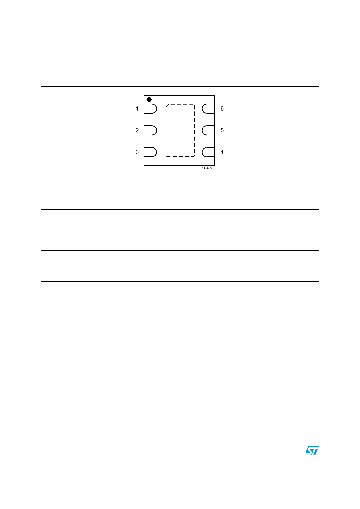
2 Pin configuration
Figure 2. Pin connections (top view)
Table 2. Pin description
Pin n° Symbol Name and function
1V
IN
Supply voltage pin
2 GND Ground
3 LX Switching pin
4V
OUT
Output voltage pin
5 FB Feedback voltage
6 EN/PWM Enable pin or PWM control input for dimming
Exposed pad GND Ground
4/23 Doc ID 010005 Rev 1
STLA02 Maximum ratings
3 Maximum ratings
Table 3. Absolute maximum ratings
Symbol Parameter Value Unit
V
IN
V
LX
FB Feedback connection
Signal supply voltage - 0.3 to 19 V
Inductor connection - 0.3 to 30 V
(1)
- 0.3 to 30 V
EN/PWM Logic pin/PWM input - 0.3 to 12 V
V
OUT
P
TOT
T
OP
T
J
T
STG
1. The maximum acceptable difference between the V
Output voltage connection - 0.3 to 30 V
Continuous power dissipation (at TA = 70 °C)
(1)
530 mW
Operating ambient temperature range - 40 to 85 °C
Junction temperature - 40 to 150 °C
Storage temperature range - 65 to 150 °C
pin potential and feedback pin potential is 5 V.
OUT
Note: Absolute maximum ratings are those values beyond which damage to the device may occur.
Functional operation under these conditions is not implied.
Table 4. Thermal data
Symbol Parameter Value Unit
R
thJA
1. Power dissipation is dependent on PCB. The recommended PCB design is included in this document (TBD).
Thermal resistance junction-ambient
(1)
102 °C/W
Table 5. ESD
Symbol Parameter Value Unit
HBM Human body model 2 kV
MM Machine model 200 V
Doc ID 010005 Rev 1 5/23
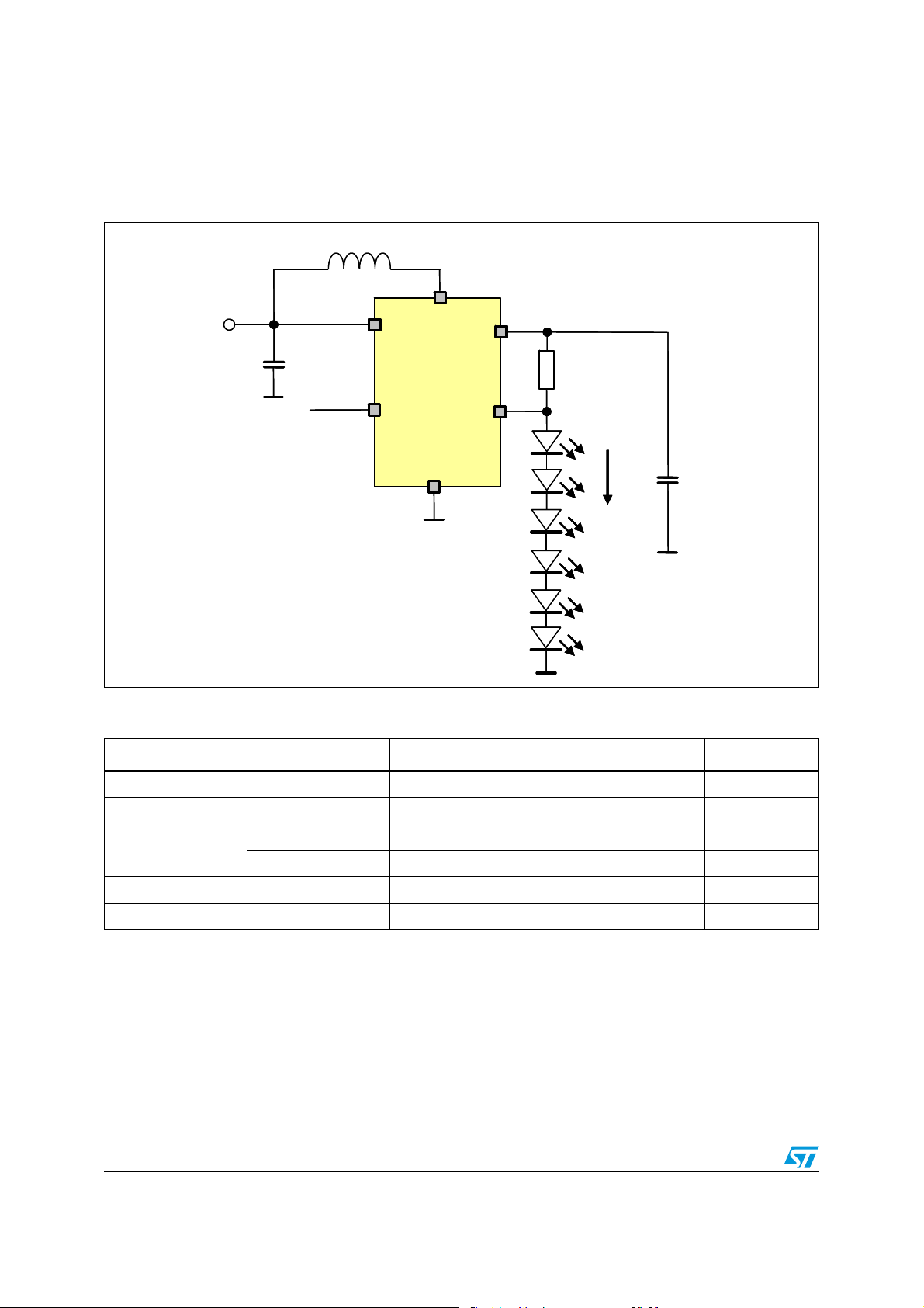
Application STLA02
4 Application
Figure 3. Application schematic
L
L
VLX
V
V
IN
IN
C
C
IN
IN
EN/PWM
EN/PWM
VIN
VIN
STLA02
STLA02
EN/PWM
EN/PWM
GND
GND
VLX
VOUT
VOUT
FB
FB
R
R
FB
FB
I
I
LED
LED
C
C
OUT
OUT
AM07828v1
AM07828v1
Table 6. List of external components
Component Manufacturer Part number Value Size
C
C
IN
OUT
MURATA GRM216R61E105KA12 1 µF / 25 V 0805
MURATA GRM216R61E105KA12 1 µF / 25 V 0805
MURATA LQH3NPN100NJ0L 10 µH 3x3x0.9 mm
L
TDK VLF3012ST-100MR59 10 µH 3x2.8x1.2 mm
R
FB
TYCO CPF0402B10RE 10 Ω 0402
LED OSRAM LWL283-Q1R2-3K8L-1-Z 20 mA / 3.1 V 0603
Note: Above listed components refer to a typical application with maximum performance settings.
Operation of the STLA02 is not limited to the choice of these external components.
6/23 Doc ID 010005 Rev 1
STLA02 Electrical characteristics
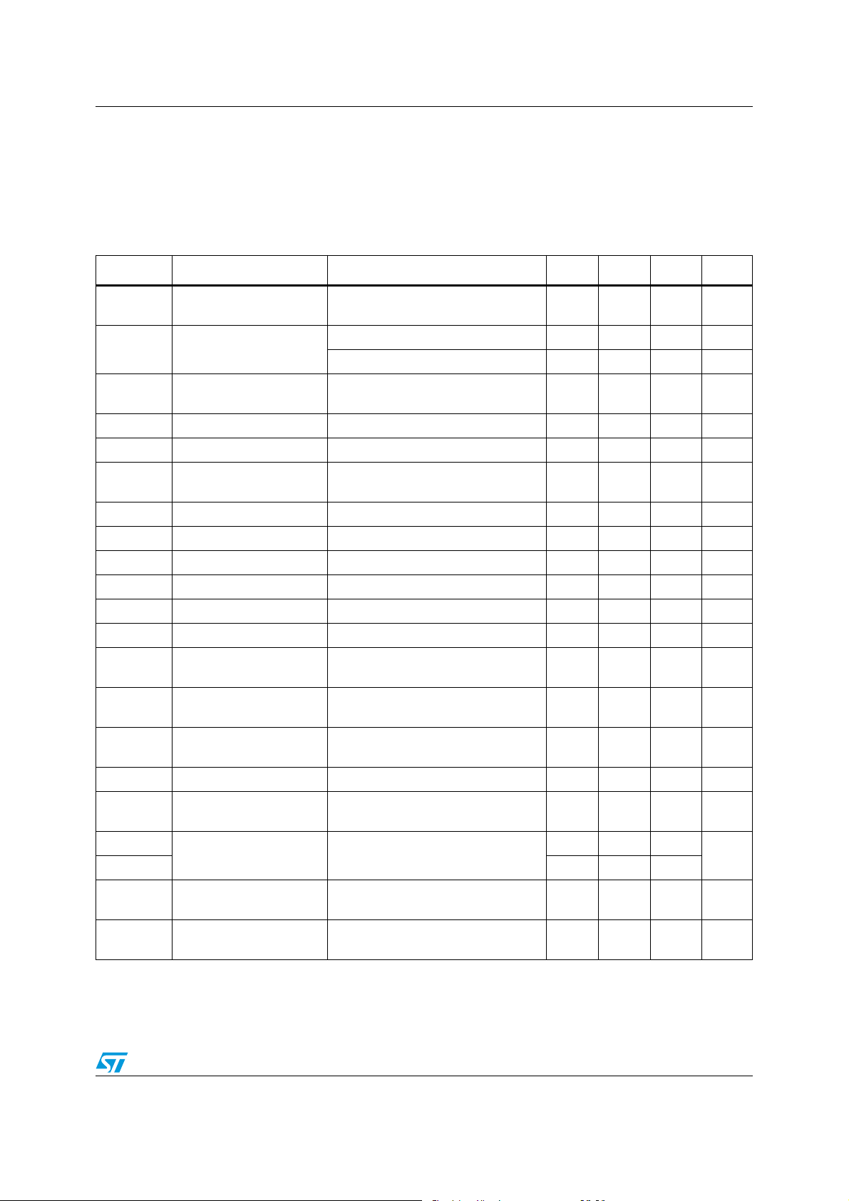
5 Electrical characteristics
V
= V
EN
T
= 25 °C, unless otherwise specified.
A
Table 7. Electrical characteristics
Symbol Parameter Test conditions Min. Typ. Max. Unit
= 3 V TA = - 40 °C to 85 °C unless otherwise specified. Typical values are at
IN
V
I
I
V
OUT
I
PEAK
V
I
FB
I
LX(leak)
ΔI
f
D
MAX
R
DSon
IN
S
O
FB
s
Input operating supply
voltage
Supply current
Output current
adjustment
Regulated voltage range V
Inductor peak current VIN = 2.5 V 300 400 550 mA
Feedback voltage (V
VFB)
FB bias current V
N-MOS leakage current V
Output current tolerance VIN = 3 V, I
O
Switching frequency V
Maximum duty cycle V
-N Internal N-channel R
ν Efficiency of the chip itself
ν
OVP
Efficiency of the whole
application
Output overvoltage
protection
V
V
V
-
OUT
V
DSonILX
V
V
V
V
V
2.5 18 V
= VIN, V
EN
= GND 10 µA
EN
= 2.5 V to 18 V, R
IN
= 2.5 V to 18 V VIN+1 27 V
IN
= VIN, R
EN
= VIN, V
EN
= 0, V
EN
= 2.5 V, TA = 25 °C 1.7 2 2.3 MHz
IN
= VIN, V
EN
= 24 V, V
OUT
= 10 Ω 190 200 210 mV
FB
= 24 V, V
OUT
LX
OUT
= V
OUT
= 24 V 0.1 µA
OUT
= 0.2 V / R
= 24 V, V
= 23 V 2 4 mA
FB
= 10 Ω 20 mA
FB
= 24 V 6 µA
FB
FB
= 24 V 88 92 %
FB
-5 5 %
= 20 mA 0.8 Ω
= 10 V, IO = 20 mA, VO = 6 x
IN
FLED_max
IN
FLED_max
IN
+ V
RSENSE
= 24 V
= 10 V, IO = 20 mA, VO = 6 x
+ V
RSENSE
= 24 V
= 3 V, no load 28 V
(1)
(1)
85 %
83 %
T
SHDN
T
HYS
V
IL
V
IH
T
EN
T
RESPONSE
1. Guaranteed by design, but not tested in production.
Thermal shutdown 130 150 °C
Thermal shutdown
hysteresis
Low and high level input
logic signal on EN pin
LED current rise time I
= 0 to I
LED
= 20 mA
LED current rise time I
= 0 mA to I
LED
LED
LED
= 20 mA
= 2.5 V to 18 V, V
V
IN
V
= 9 V, V
IN
series
V
= 9 V, V
IN
series
Doc ID 010005 Rev 1 7/23
(1)
(1)
ENMAX
= 0 V to 3 V 6 LEDs in
EN
= 0 V to 3 V, 6 LEDs in
EN
, V
precharged
OUT
= 12 V
15 °C
01.5
V
1.8 V
IN
0.2 ms
60 µs

Typical performance characteristics STLA02
6 Typical performance characteristics
Figure 4. Efficiency at 20 mA current load
STLA02 20 mA / 18 V eff.
STLA02 20 mA / 18 V eff.
IN [mA]
IN [mA]
92
92
89
89
86
86
83
83
80
80
77
77
74
74
71
71
Eff [%]
Eff [%]
68
68
65
65
62
62
59
59
56
56
53
53
50
50
2 3 4 5 6 7 8 9 10 11 12 13 14 15
2 3 4 5 6 7 8 9 10 11 12 13 14 15
VIN[V]
VIN[V]
AM07819v1
AM07819v1
200
200
150
150
100
100
50
50
0
0
IIN[mA]
IIN[mA]
Figure 5. Quiescent current vs. V
20
20
15
15
[µA]
[µA]
10
10
IN
IN
I
I
5
5
0
0
0 2 4 6 8 101214161820
0 2 4 6 8 101214161820
IN
AM07820v1
AM07820v1
[V]
[V]
V
V
IN
IN
8/23 Doc ID 010005 Rev 1

STLA02 Typical performance characteristics
Figure 6. STLA02 driver current consumption vs. V
1.80
1.80
1.60
1.60
1.40
1.40
[mA]
[mA]
1.20
1.20
IN
IN
I
I
1.00
1.00
0.80
0.80
0.60
0.60
0.00 2.00 4.00 6.00 8.00 10.00 12.00 14.00 16.00 18.00 20.00
0.00 2.00 4.00 6.00 8.00 10.00 12.00 14.00 16.00 18.00 20.00
V
V
IN
IN
Figure 7. Switching frequency vs. temperature
2
2
8
8
9
9
,
,
1
1
[V]
[V]
IN
25°C-40°C+85°C
25°C-40°C+85°C
AM07821v1
AM07821v1
AM07822v1
AM07822v1
6
6
9
9
,
,
1
F [MHz]
F [MHz]
-60 -40 -20 0 20 40 60 80 100
-60 -40 -20 0 20 40 60 80 100
1
4
4
9
9
,
,
1
1
2
2
9
9
,
,
1
1
9
9
,
,
1
1
Temp [°C]
Temp [°C]
Doc ID 010005 Rev 1 9/23

Typical performance characteristics STLA02
Figure 8. Switching frequency vs. V
2.0
2.0
1.9
1.9
1.8
1.8
1.7
1.7
1.6
1.6
1.5
1.5
1.4
1.4
1.3
1.3
F [MHz]
F [MHz]
1.2
1.2
1.1
1.1
1.0
1.0
0.9
0.9
0.8
0.8
0.7
0.7
0.6
0.6
0.5
0.5
0.4
0.4
234567891011121314
234567891011121314
Figure 9. Overvoltage protection threshold vs. V
30.0
30.0
IN
@ P
= 0.36 W
OUT
AM07823v1
AM07823v1
V
V
[V]
[V]
IN
IN
IN
AM07824v1
AM07824v1
29.5
29.5
29.0
29.0
28.5
28.5
28.0
28.0
[V]
[V]
OUT
OUT
27.5
27.5
V
V
27.0
27.0
26.5
26.5
26.0
26.0
25.5
25.5
25.0
25.0
2 3 4 5 6 7 8 9 10 11 12 13 14 15 16 17 18
2 3 4 5 6 7 8 9 10 11 12 13 14 15 16 17 18
[V]
[V]
V
V
IN
IN
10/23 Doc ID 010005 Rev 1

STLA02 Typical performance characteristics
Figure 10. Overvoltage protection threshold vs. temp
AM07825v1
0
0
.
.
0
0
3
3
5
5
.
.
9
9
2
2
0
0
.
.
9
9
2
2
5
5
.
.
8
8
2
2
0
0
.
.
8
[V]
[V]
OUT
OUT
V
V
-40-30-20-100 1020304050607080
-40-30-20-100 1020304050607080
8
2
2
5
5
.
.
7
7
2
2
0
0
.
.
7
7
2
2
5
5
.
.
6
6
2
2
0
0
.
.
6
6
2
2
5
5
.
.
5
5
2
2
0
0
.
.
5
5
2
2
Temp [°C]
Temp [°C]
AM07825v1
Figure 11. Output current regulation vs. V
21.0
21.0
20.8
20.8
20.6
20.6
20.4
20.4
20.2
20.2
20.0
20.0
19.8
19.8
19.6
19.6
19.4
19.4
19.2
19.2
[mA]
[mA]
19.0
19.0
OUT
OUT
I
I
18.8
18.8
18.6
18.6
18.4
18.4
18.2
18.2
18.0
18.0
17.8
17.8
17.6
17.6
17.4
17.4
17.2
17.2
17.0
17.0
0
0
2 4 6 8 10 12 14 16 18
2 4 6 8 10 12 14 16 18
IN
AM07826v1
AM07826v1
[V]
[V]
V
V
IN
IN
Doc ID 010005 Rev 1 11/23

Typical performance characteristics STLA02
IOUT
IOUT
VOUT
VOUT
VOUT
VOUT
VLX
VLX
= 2.5 V Figure 13. Switching waveform at V
IN
IL
IL
IOUT
IOUT
IL
IL
VOUT
VOUT
VOUT
VOUT
VLX
VLX
IL
IL
IL
IL
Figure 12. Switching waveform at V
Figure 14. Switching waveform at VIN = 12 V Figure 15. Overvoltage function
IOUT
IOUT
IN
= 7 V
VLX
VLX
Figure 16. Line transient response V
VIN
VIN
IL
IL
= 3.4 V to 4 V step
IN
IOUT
IOUT
VLX
VLX
VLX
VLX
12/23 Doc ID 010005 Rev 1

STLA02 Typical performance characteristics
Figure 17. Direct PWM dimming 300 Hz at V
BAT
= 2.5 V, V
= 0 to 3 V step
EN
Doc ID 010005 Rev 1 13/23

Introduction STLA02
(
)
7 Introduction
The STLA02 is a boost converter dedicated to powering and controlling the current of white
LEDs in an LCD backlight. The device operates at a typical constant switching frequency of
2.3 MHz. It steps an input voltage ranging from 2.5 V to 18 V, up to 27 V. The output current
is adjustable by the resistor R
device contains high side sensing to simplify the PCB layout in terms of connection of the
LEDs.
The output current is dimmable by the PWM signal applied to the EN pin with minimum
PWM frequency equal 100 Hz.
7.1 PWM input (EN)
Light intensity can be dimmed by a signal applied to the PWM (EN) input.
The PWM signal is directly connected to the enable pin of the STLA02. It is recommended
to use the frequency of the PWM signal in the range of 100 Hz to 1 kHz and amplitude of the
signal 1.8 V min. The result of the direct PWM dimming method (300 Hz PWM and V
1.8 V) is shown in
Figure 17.
connected between the V
FB
and FB pins. The STLA02
OUT
EN
=
Note: When the device is required to operate in a constant current mode with the EN pin
connected to the voltage higher than 1.8 V, then the delay between rise times of V
of the device and the EN voltage is mandatory to guarantee the proper internal reset of the
logic of the device during ramping of the V
time by 2 ms after the rise time on V
IN
. It is recommended to delay the EN voltage rise
IN
appears.
7.2 Selection of the external components
CIN selection
It is recommended to use 1 µF as the input capacitor to achieve good stability of the device
and low noise on the V
C
selection
OUT
It is recommended to use 1 µF as the optimal value of output capacitor to get the best
compromise between output voltage ripple and load transients response. The output ripple
can be checked according to the equation for step-up architecture:
Equation 1
track.
IN
V
=
−
PKPK
−∗
2
OUTOUT
100*VVI
)MIN(INOUT)MAX(OUT
fVC
∗∗
[]
Hz,F,V,A;V
voltage
IN
Inductor selection
A thin shielded inductor with a low DC series winding resistance is recommended for this
application. To achieve a good efficiency in step-up mode, it is recommended to use an
inductor with a DC series resistance R
resistance of the LED [
14/23 Doc ID 010005 Rev 1
Ω; Ω; 1].
= RD/10 [Ω; Ω; 1], where RD is the dynamic
DCL

STLA02 Introduction
[
For nominal operation, the peak inductor current can be calculated by the formula:
Equation 2
VfL2
∗−
OUT
2
⎫
]
VVVI
V
⎪
ININOUTOUT
2
OUT
⎬
V
⎪
IN
⎭
I ∗
PEAK
⎜
⎨
ν
⎪
⎝
⎩
⎧
⎛
⎪
=
()
⎞
+
⎟
⎠
∗∗∗
where:
I
Peak inductor current
PEAK
I
Current sourced at the V
OUT
OUT
pin
ν Efficiency of the STLA02
V
Output voltage at the V
OUT
V
Input voltage at the V
IN
IN
OUT
pin
pin
L Inductance value of the inductor
f Switching frequency
For the optimal function of the STLA02 device, it is recommended to use the inductor value
10 µH and higher with low serial resistance and relevant saturation current calculated from
the equation above.
RFB value
RFB = VFB / I
In the case of a typical setting I
resistor must be rated for a power dissipation of 10 x 0.02² W = 0.004 W.
LED
= 20 mA, VFB = 200 mV, and R
LED
SENSE
= 10 Ω. The
PCB layout
STLA02 is a powerful switched device, the PCB must be designed in line with rules for
designing switched supplies. It is recommended to use a two layer PCB. The power wirings
must be as short as possible and wide. Place all external components close to the STLA02.
High-energy switched loops should be as small as possible to reduce EMI. Most LEDs need
cooling, which may be done by a defined area of copper on the PCB. Use the reference
guide of each LED to design the heatsink. Place the R
4 and 5. When a change of PCB layer is needed, use enough vias. During routing the PCB
must be focused on the minimum area of the application ground - the smaller the ground
area of the DC-DC converter
(a)
, the better stability and lower noise issues are achieved. It is
recommended to place the copper plate, connected through the vias to the Exposed pad, on
the bottom layer to create the heatsink of the device.
a. The application ground area is represented by the area which is created by the ground pins of the CIN, C
ground of the DEVICE and GND connection of the load.
Doc ID 010005 Rev 1 15/23
resistor as close as possible to pin
FB
OUT
,

Introduction STLA02
Figure 18. Top layer
Figure 19. Bottom layer
16/23 Doc ID 010005 Rev 1

STLA02 Introduction
Figure 20. Top overlay
Doc ID 010005 Rev 1 17/23

Package mechanical data STLA02
8 Package mechanical data
In order to meet environmental requirements, ST offers these devices in different grades of
ECOPACK
specifications, grade definitions, and product status are available at
is an ST trademark.
®
packages, depending on their level of environmental compliance. ECOPACK
www.st.com. ECOPACK
18/23 Doc ID 010005 Rev 1

STLA02 Package mechanical data
Table 8. DFN6 (2 x 2 mm.) mechanical data
mm.
Dim.
Min. Typ. Max.
A 0.700.750.80
A1 0 0.02 0.05
A3 0.20
b 0.180.250.30
D 1.902.002.10
D2 1.35 1.50 1.60
E 1.902.002.10
E2 0.15 0.30 0.40
e0.50
L 0.250.350.45
Figure 21. DFN6 (2 x 2 mm.) drawing
7733060D
Doc ID 010005 Rev 1 19/23

Package mechanical data STLA02
Table 9. DFN6 (2 x 2 mm.) tape and reel mechanical data
mm. inch.
Dim.
Min. Typ. Max. Min. Typ. Max.
A 180 7.087
C 12.8 13.2 0.504 0.519
D 20.2 0.795
N 60 2.362
T 14.4 0.567
Ao 2.3 0.091
Bo 2.3 0.091
Ko 1.0 0.039
Po 4 0.157
P 8 0.315
Figure 22. DFN6 (2 x 2 mm.) tape and reel drawing
20/23 Doc ID 010005 Rev 1

STLA02 Package mechanical data
Figure 23. DFN6 (2 x 2 mm) footprint recommended data
Doc ID 010005 Rev 1 21/23

Revision history STLA02
9 Revision history
Table 10. Document revision history
Date Revision Changes
22-Feb-2011 1 Initial release
22/23 Doc ID 010005 Rev 1

STLA02
Please Read Carefully:
Information in this document is provided solely in connection with ST products. STMicroelectronics NV and its subsidiaries (“ST”) reserve the
right to make changes, corrections, modifications or improvements, to this document, and the products and services described herein at any
time, without notice.
All ST products are sold pursuant to ST’s terms and conditions of sale.
Purchasers are solely responsible for the choice, selection and use of the ST products and services described herein, and ST assumes no
liability whatsoever relating to the choice, selection or use of the ST products and services described herein.
No license, express or implied, by estoppel or otherwise, to any intellectual property rights is granted under this document. If any part of this
document refers to any third party products or services it shall not be deemed a license grant by ST for the use of such third party products
or services, or any intellectual property contained therein or considered as a warranty covering the use in any manner whatsoever of such
third party products or services or any intellectual property contained therein.
UNLESS OTHERWISE SET FORTH IN ST’S TERMS AND CONDITIONS OF SALE ST DISCLAIMS ANY EXPRESS OR IMPLIED
WARRANTY WITH RESPECT TO THE USE AND/OR SALE OF ST PRODUCTS INCLUDING WITHOUT LIMITATION IMPLIED
WARRANTIES OF MERCHANTABILITY, FITNESS FOR A PARTICULAR PURPOSE (AND THEIR EQUIVALENTS UNDER THE LAWS
OF ANY JURISDICTION), OR INFRINGEMENT OF ANY PATENT, COPYRIGHT OR OTHER INTELLECTUAL PROPERTY RIGHT.
UNLESS EXPRESSLY APPROVED IN WRITING BY AN AUTHORIZED ST REPRESENTATIVE, ST PRODUCTS ARE NOT
RECOMMENDED, AUTHORIZED OR WARRANTED FOR USE IN MILITARY, AIR CRAFT, SPACE, LIFE SAVING, OR LIFE SUSTAINING
APPLICATIONS, NOR IN PRODUCTS OR SYSTEMS WHERE FAILURE OR MALFUNCTION MAY RESULT IN PERSONAL INJURY,
DEATH, OR SEVERE PROPERTY OR ENVIRONMENTAL DAMAGE. ST PRODUCTS WHICH ARE NOT SPECIFIED AS "AUTOMOTIVE
GRADE" MAY ONLY BE USED IN AUTOMOTIVE APPLICATIONS AT USER’S OWN RISK.
Resale of ST products with provisions different from the statements and/or technical features set forth in this document shall immediately void
any warranty granted by ST for the ST product or service described herein and shall not create or extend in any manner whatsoever, any
liability of ST.
ST and the ST logo are trademarks or registered trademarks of ST in various countries.
Information in this document supersedes and replaces all information previously supplied.
The ST logo is a registered trademark of STMicroelectronics. All other names are the property of their respective owners.
© 2011 STMicroelectronics - All rights reserved
STMicroelectronics group of companies
Australia - Belgium - Brazil - Canada - China - Czech Republic - Finland - France - Germany - Hong Kong - India - Israel - Italy - Japan -
Malaysia - Malta - Morocco - Philippines - Singapore - Spain - Sweden - Switzerland - United Kingdom - United States of America
www.st.com
Doc ID 010005 Rev 1 23/23
 Loading...