

8-bit MCU for automotive with Flash or ROM,
LQFP32 7x7mm
LQFP44 10x10mm
LQFP64 10x10mm
Features
■ Memories
– 16 K to 60 K High Density Flash (HDFlash)
or ROM with read-out protection capability.
In-application programming and in-circuit
programming for HDFlash devices
– 1.5 to 2 K RAM
– HDFlash endurance: 100 cycles, data
retention 20 years at 55 °C
■ Clock, reset and supply management
–Low power crystal/ceramic resonator
oscillators and bypass for external clock
– PLL for 2 x frequency multiplication
– 5 power saving modes: halt, auto wake up
from halt, active halt, wait and slow
■ Interrupt management
– Nested interrupt controller
– 14 interrupt vectors plus TRAP and RESET
– TLI top level interrupt (on 64-pin devices)
– Up to 21 external interrupt lines (on 4
vectors)
■ Up to 48 I/O ports
– Up to 48 multifunctional bidirectional I/O
lines
– Up to 36 alternate function lines
– Up to 6 high sink outputs
■ 5 timers
– 16-bit timer with 2 input captures, 2 output
compares, external clock input, PWM and
pulse generator modes
– 8-bit timer with 1 or 2 input captures, 1 or 2
output compares, PWM and pulse
generator modes
– 8-bit PWM auto-reload timer with 1 or 2
input captures, 2 or 4 independent PWM
output channels, output compare and time
base interrupt, external clock with event
detector
ST72361xx-Auto
10-bit ADC, 5 timers, SPI, LINSCI™
– Main clock controller with real-time base
and clock output
– Window watchdog timer
■ Up to 3 communications interfaces
– SPI synchronous serial interface
– Master/ slave LINSCI™ asynchronous
serial interface
– Master only LINSCI™ asynchronous serial
interface
■ Analog peripheral (low current coupling)
– 10-bit A/D converter with up to 16 inputs
– Up to 9 robust ports (low current coupling)
■ Instruction set
– 8-bit data manipulation
– 63 basic instructions
– 17 main addressing modes
– 8 x 8 unsigned multiply instruction
■ Development tools
– Full hardware/ software development
package
Table 1. Device summary
Reference Part number
ST72361K4-Auto, ST72361K6-Auto,
ST72361K7-Auto, ST72361K9-Auto,
ST72361xx
-Auto
ST72361J4-Auto, ST72361J6-Auto,
ST72361J7-Auto, ST72361J9-Auto,
ST72361AR4-Auto, ST72361AR6-Auto,
ST72361AR7-Auto, ST72361AR9-Auto
August 2010 Doc ID 12468 Rev 3 1/279
www.st.com
1

Contents ST72361xx-Auto
Contents
1 Description . . . . . . . . . . . . . . . . . . . . . . . . . . . . . . . . . . . . . . . . . . . . . . . . 19
1.1 Pin description . . . . . . . . . . . . . . . . . . . . . . . . . . . . . . . . . . . . . . . . . . . . . 21
2 Register and memory map . . . . . . . . . . . . . . . . . . . . . . . . . . . . . . . . . . . 27
3 Flash program memory . . . . . . . . . . . . . . . . . . . . . . . . . . . . . . . . . . . . . 30
3.1 Introduction . . . . . . . . . . . . . . . . . . . . . . . . . . . . . . . . . . . . . . . . . . . . . . . 30
3.2 Main features . . . . . . . . . . . . . . . . . . . . . . . . . . . . . . . . . . . . . . . . . . . . . . 30
3.3 Structure . . . . . . . . . . . . . . . . . . . . . . . . . . . . . . . . . . . . . . . . . . . . . . . . . . 30
3.3.1 Read-out protection . . . . . . . . . . . . . . . . . . . . . . . . . . . . . . . . . . . . . . . . 31
3.4 ICC interface . . . . . . . . . . . . . . . . . . . . . . . . . . . . . . . . . . . . . . . . . . . . . . 31
3.5 ICP (in-circuit programming) . . . . . . . . . . . . . . . . . . . . . . . . . . . . . . . . . . 32
3.6 IAP (in-application programming) . . . . . . . . . . . . . . . . . . . . . . . . . . . . . . . 33
3.7 Related documentation . . . . . . . . . . . . . . . . . . . . . . . . . . . . . . . . . . . . . . 33
3.8 Register description . . . . . . . . . . . . . . . . . . . . . . . . . . . . . . . . . . . . . . . . . 33
4 Central processing unit . . . . . . . . . . . . . . . . . . . . . . . . . . . . . . . . . . . . . 34
4.1 Introduction . . . . . . . . . . . . . . . . . . . . . . . . . . . . . . . . . . . . . . . . . . . . . . . 34
4.2 Main features . . . . . . . . . . . . . . . . . . . . . . . . . . . . . . . . . . . . . . . . . . . . . . 34
4.3 CPU registers . . . . . . . . . . . . . . . . . . . . . . . . . . . . . . . . . . . . . . . . . . . . . . 34
4.3.1 Accumulator (A) . . . . . . . . . . . . . . . . . . . . . . . . . . . . . . . . . . . . . . . . . . . 34
4.3.2 Index registers (X and Y) . . . . . . . . . . . . . . . . . . . . . . . . . . . . . . . . . . . . 34
4.3.3 Program counter (PC) . . . . . . . . . . . . . . . . . . . . . . . . . . . . . . . . . . . . . . 34
4.3.4 Condition code register (CC) . . . . . . . . . . . . . . . . . . . . . . . . . . . . . . . . . 35
4.3.5 Stack pointer (SP) . . . . . . . . . . . . . . . . . . . . . . . . . . . . . . . . . . . . . . . . . 37
5 Supply, reset and clock management . . . . . . . . . . . . . . . . . . . . . . . . . . 39
5.1 Introduction . . . . . . . . . . . . . . . . . . . . . . . . . . . . . . . . . . . . . . . . . . . . . . . 39
5.2 Main features . . . . . . . . . . . . . . . . . . . . . . . . . . . . . . . . . . . . . . . . . . . . . . 39
5.3 Phase locked loop . . . . . . . . . . . . . . . . . . . . . . . . . . . . . . . . . . . . . . . . . . 39
5.4 Multi-oscillator (MO) . . . . . . . . . . . . . . . . . . . . . . . . . . . . . . . . . . . . . . . . . 40
5.5 Reset sequence manager (RSM) . . . . . . . . . . . . . . . . . . . . . . . . . . . . . . . 41
5.5.1 Introduction . . . . . . . . . . . . . . . . . . . . . . . . . . . . . . . . . . . . . . . . . . . . . . 41
2/279 Doc ID 12468 Rev 3

ST72361xx-Auto Contents
5.5.2 Asynchronous external RESET pin . . . . . . . . . . . . . . . . . . . . . . . . . . . . 42
5.5.3 External power-on reset . . . . . . . . . . . . . . . . . . . . . . . . . . . . . . . . . . . . . 42
5.5.4 Internal low voltage detector (LVD) reset . . . . . . . . . . . . . . . . . . . . . . . . 42
5.5.5 Internal watchdog reset . . . . . . . . . . . . . . . . . . . . . . . . . . . . . . . . . . . . . 43
5.6 System integrity management (SI) . . . . . . . . . . . . . . . . . . . . . . . . . . . . . . 43
5.6.1 Low voltage detector (LVD) . . . . . . . . . . . . . . . . . . . . . . . . . . . . . . . . . . 43
5.6.2 Auxiliary voltage detector (AVD) . . . . . . . . . . . . . . . . . . . . . . . . . . . . . . 44
5.6.3 Low power modes . . . . . . . . . . . . . . . . . . . . . . . . . . . . . . . . . . . . . . . . . 45
5.6.4 Interrupts . . . . . . . . . . . . . . . . . . . . . . . . . . . . . . . . . . . . . . . . . . . . . . . . 45
5.6.5 Register description . . . . . . . . . . . . . . . . . . . . . . . . . . . . . . . . . . . . . . . . 46
6 Interrupts . . . . . . . . . . . . . . . . . . . . . . . . . . . . . . . . . . . . . . . . . . . . . . . . . 48
6.1 Introduction . . . . . . . . . . . . . . . . . . . . . . . . . . . . . . . . . . . . . . . . . . . . . . . 48
6.2 Masking and processing flow . . . . . . . . . . . . . . . . . . . . . . . . . . . . . . . . . . 48
6.3 Interrupts and low power modes . . . . . . . . . . . . . . . . . . . . . . . . . . . . . . . 51
6.4 Concurrent & nested management . . . . . . . . . . . . . . . . . . . . . . . . . . . . . 51
6.5 Interrupt register description . . . . . . . . . . . . . . . . . . . . . . . . . . . . . . . . . . 52
6.5.1 CPU CC register interrupt bits . . . . . . . . . . . . . . . . . . . . . . . . . . . . . . . . 52
6.5.2 Interrupt software priority registers (ISPRX) . . . . . . . . . . . . . . . . . . . . . 53
6.6 External interrupts . . . . . . . . . . . . . . . . . . . . . . . . . . . . . . . . . . . . . . . . . . 56
6.6.1 I/O port interrupt sensitivity . . . . . . . . . . . . . . . . . . . . . . . . . . . . . . . . . . 56
6.6.2 Register description . . . . . . . . . . . . . . . . . . . . . . . . . . . . . . . . . . . . . . . . 58
7 Power saving modes . . . . . . . . . . . . . . . . . . . . . . . . . . . . . . . . . . . . . . . . 61
7.1 Introduction . . . . . . . . . . . . . . . . . . . . . . . . . . . . . . . . . . . . . . . . . . . . . . . 61
7.2 Slow mode . . . . . . . . . . . . . . . . . . . . . . . . . . . . . . . . . . . . . . . . . . . . . . . . 61
7.3 Wait mode . . . . . . . . . . . . . . . . . . . . . . . . . . . . . . . . . . . . . . . . . . . . . . . . 62
7.4 Halt mode . . . . . . . . . . . . . . . . . . . . . . . . . . . . . . . . . . . . . . . . . . . . . . . . . 63
7.5 Active halt mode . . . . . . . . . . . . . . . . . . . . . . . . . . . . . . . . . . . . . . . . . . . . 65
7.6 Auto wake-up from halt mode . . . . . . . . . . . . . . . . . . . . . . . . . . . . . . . . . . 66
7.6.1 Register description . . . . . . . . . . . . . . . . . . . . . . . . . . . . . . . . . . . . . . . . 69
8 I/O ports . . . . . . . . . . . . . . . . . . . . . . . . . . . . . . . . . . . . . . . . . . . . . . . . . . 71
8.1 Introduction . . . . . . . . . . . . . . . . . . . . . . . . . . . . . . . . . . . . . . . . . . . . . . . 71
8.2 Functional description . . . . . . . . . . . . . . . . . . . . . . . . . . . . . . . . . . . . . . . 71
8.2.1 Input modes . . . . . . . . . . . . . . . . . . . . . . . . . . . . . . . . . . . . . . . . . . . . . . 71
Doc ID 12468 Rev 3 3/279

Contents ST72361xx-Auto
8.2.2 Output modes . . . . . . . . . . . . . . . . . . . . . . . . . . . . . . . . . . . . . . . . . . . . 72
8.2.3 Alternate functions . . . . . . . . . . . . . . . . . . . . . . . . . . . . . . . . . . . . . . . . . 72
8.3 I/O port implementation . . . . . . . . . . . . . . . . . . . . . . . . . . . . . . . . . . . . . . 75
8.4 I/O port register configurations . . . . . . . . . . . . . . . . . . . . . . . . . . . . . . . . . 75
8.4.1 Standard ports . . . . . . . . . . . . . . . . . . . . . . . . . . . . . . . . . . . . . . . . . . . . 75
8.4.2 Interrupt ports . . . . . . . . . . . . . . . . . . . . . . . . . . . . . . . . . . . . . . . . . . . . 76
8.4.3 Pull-up input port . . . . . . . . . . . . . . . . . . . . . . . . . . . . . . . . . . . . . . . . . 77
8.5 Low power modes . . . . . . . . . . . . . . . . . . . . . . . . . . . . . . . . . . . . . . . . . . 78
8.6 Interrupts . . . . . . . . . . . . . . . . . . . . . . . . . . . . . . . . . . . . . . . . . . . . . . . . . 78
9 Window watchdog (WWDG) . . . . . . . . . . . . . . . . . . . . . . . . . . . . . . . . . . 80
9.1 Introduction . . . . . . . . . . . . . . . . . . . . . . . . . . . . . . . . . . . . . . . . . . . . . . . 80
9.2 Main features . . . . . . . . . . . . . . . . . . . . . . . . . . . . . . . . . . . . . . . . . . . . . . 80
9.3 Functional description . . . . . . . . . . . . . . . . . . . . . . . . . . . . . . . . . . . . . . . 80
9.4 Using halt mode with the WDG . . . . . . . . . . . . . . . . . . . . . . . . . . . . . . . . 82
9.5 How to program the watchdog timeout . . . . . . . . . . . . . . . . . . . . . . . . . . . 82
9.6 Low power modes . . . . . . . . . . . . . . . . . . . . . . . . . . . . . . . . . . . . . . . . . . 84
9.7 Hardware watchdog option . . . . . . . . . . . . . . . . . . . . . . . . . . . . . . . . . . . . 84
9.8 Using halt mode with the WDG (WDGHALT option) . . . . . . . . . . . . . . . . 85
9.9 Interrupts . . . . . . . . . . . . . . . . . . . . . . . . . . . . . . . . . . . . . . . . . . . . . . . . . 85
9.10 Register description . . . . . . . . . . . . . . . . . . . . . . . . . . . . . . . . . . . . . . . . . 85
9.10.1 Control register (WDGCR) . . . . . . . . . . . . . . . . . . . . . . . . . . . . . . . . . . . 85
9.10.2 Window Register (WDGWR) . . . . . . . . . . . . . . . . . . . . . . . . . . . . . . . . . 85
10 Main clock controller with real time clock MCC/RTC . . . . . . . . . . . . . . 87
10.1 Programmable CPU clock prescaler . . . . . . . . . . . . . . . . . . . . . . . . . . . . 87
10.2 Clock-out capability . . . . . . . . . . . . . . . . . . . . . . . . . . . . . . . . . . . . . . . . . 87
10.3 Real time clock timer (RTC) . . . . . . . . . . . . . . . . . . . . . . . . . . . . . . . . . . . 87
10.4 Low power modes . . . . . . . . . . . . . . . . . . . . . . . . . . . . . . . . . . . . . . . . . . 88
10.5 Interrupts . . . . . . . . . . . . . . . . . . . . . . . . . . . . . . . . . . . . . . . . . . . . . . . . . 88
10.6 Register description . . . . . . . . . . . . . . . . . . . . . . . . . . . . . . . . . . . . . . . . . 88
10.6.1 MCC control/status register (MCCSR) . . . . . . . . . . . . . . . . . . . . . . . . . . 88
11 PWM auto-reload timer (ART) . . . . . . . . . . . . . . . . . . . . . . . . . . . . . . . . 91
11.1 Introduction . . . . . . . . . . . . . . . . . . . . . . . . . . . . . . . . . . . . . . . . . . . . . . . 91
4/279 Doc ID 12468 Rev 3

ST72361xx-Auto Contents
11.2 Functional description . . . . . . . . . . . . . . . . . . . . . . . . . . . . . . . . . . . . . . . 92
11.2.1 Counter . . . . . . . . . . . . . . . . . . . . . . . . . . . . . . . . . . . . . . . . . . . . . . . . . 92
11.2.2 Counter clock and prescaler . . . . . . . . . . . . . . . . . . . . . . . . . . . . . . . . . 92
11.2.3 Counter and prescaler Initialization . . . . . . . . . . . . . . . . . . . . . . . . . . . . 92
11.2.4 Output compare control . . . . . . . . . . . . . . . . . . . . . . . . . . . . . . . . . . . . . 92
11.2.5 Independent PWM signal generation . . . . . . . . . . . . . . . . . . . . . . . . . . . 93
11.2.6 Output compare and Time base interrupt . . . . . . . . . . . . . . . . . . . . . . . 94
11.2.7 External clock and event detector mode . . . . . . . . . . . . . . . . . . . . . . . . 94
11.2.8 Input capture function . . . . . . . . . . . . . . . . . . . . . . . . . . . . . . . . . . . . . . 94
11.2.9 External interrupt capability . . . . . . . . . . . . . . . . . . . . . . . . . . . . . . . . . . 96
11.3 Register description . . . . . . . . . . . . . . . . . . . . . . . . . . . . . . . . . . . . . . . . . 97
12 16-bit timer . . . . . . . . . . . . . . . . . . . . . . . . . . . . . . . . . . . . . . . . . . . . . . . 102
12.1 Introduction . . . . . . . . . . . . . . . . . . . . . . . . . . . . . . . . . . . . . . . . . . . . . . 102
12.2 Main features . . . . . . . . . . . . . . . . . . . . . . . . . . . . . . . . . . . . . . . . . . . . . 102
12.3 Functional description . . . . . . . . . . . . . . . . . . . . . . . . . . . . . . . . . . . . . . 103
12.3.1 Counter . . . . . . . . . . . . . . . . . . . . . . . . . . . . . . . . . . . . . . . . . . . . . . . . 103
12.3.2 External clock . . . . . . . . . . . . . . . . . . . . . . . . . . . . . . . . . . . . . . . . . . . 105
12.3.3 Input capture . . . . . . . . . . . . . . . . . . . . . . . . . . . . . . . . . . . . . . . . . . . . 106
12.3.4 Procedure . . . . . . . . . . . . . . . . . . . . . . . . . . . . . . . . . . . . . . . . . . . . . . 107
12.3.5 Output compare . . . . . . . . . . . . . . . . . . . . . . . . . . . . . . . . . . . . . . . . . . 108
12.3.6 Procedure . . . . . . . . . . . . . . . . . . . . . . . . . . . . . . . . . . . . . . . . . . . . . . 109
12.3.7 Forced compare output capability . . . . . . . . . . . . . . . . . . . . . . . . . . . . 110
12.3.8 One pulse mode . . . . . . . . . . . . . . . . . . . . . . . . . . . . . . . . . . . . . . . . . 111
12.3.9 Pulse width modulation mode . . . . . . . . . . . . . . . . . . . . . . . . . . . . . . . 113
12.4 Low power modes . . . . . . . . . . . . . . . . . . . . . . . . . . . . . . . . . . . . . . . . . 115
12.5 Interrupts . . . . . . . . . . . . . . . . . . . . . . . . . . . . . . . . . . . . . . . . . . . . . . . . 115
12.6 Summary of timer modes . . . . . . . . . . . . . . . . . . . . . . . . . . . . . . . . . . . . 116
12.7 Register description . . . . . . . . . . . . . . . . . . . . . . . . . . . . . . . . . . . . . . . . 116
12.7.1 Control register 1 (CR1) . . . . . . . . . . . . . . . . . . . . . . . . . . . . . . . . . . . . 116
12.7.2 Control register 2 (CR2) . . . . . . . . . . . . . . . . . . . . . . . . . . . . . . . . . . . . 117
12.7.3 Control/status register (CSR) . . . . . . . . . . . . . . . . . . . . . . . . . . . . . . . . 118
12.7.4 Input capture 1 high register (IC1HR) . . . . . . . . . . . . . . . . . . . . . . . . . 119
12.7.5 Input capture 1 low register (IC1LR) . . . . . . . . . . . . . . . . . . . . . . . . . . 120
12.7.6 Output compare 1 high register (OC1HR) . . . . . . . . . . . . . . . . . . . . . . 120
12.7.7 Output compare 1 low register (OC1LR) . . . . . . . . . . . . . . . . . . . . . . . 120
Doc ID 12468 Rev 3 5/279

Contents ST72361xx-Auto
12.7.8 Output compare 2 high register (OC2HR) . . . . . . . . . . . . . . . . . . . . . . 120
12.7.9 Output compare 2 low register (OC2LR) . . . . . . . . . . . . . . . . . . . . . . . 121
12.7.10 Counter high register (CHR) . . . . . . . . . . . . . . . . . . . . . . . . . . . . . . . . 121
12.7.11 Counter low register (CLR) . . . . . . . . . . . . . . . . . . . . . . . . . . . . . . . . . 121
12.7.12 Alternate counter high register (ACHR) . . . . . . . . . . . . . . . . . . . . . . . . 121
12.7.13 Alternate counter low register (ACLR) . . . . . . . . . . . . . . . . . . . . . . . . . 122
12.7.14 Input capture 2 high register (IC2HR) . . . . . . . . . . . . . . . . . . . . . . . . . 122
12.7.15 Input capture 2 low register (IC2LR) . . . . . . . . . . . . . . . . . . . . . . . . . . 122
13 8-bit timer (TIM8) . . . . . . . . . . . . . . . . . . . . . . . . . . . . . . . . . . . . . . . . . . 124
13.1 Introduction . . . . . . . . . . . . . . . . . . . . . . . . . . . . . . . . . . . . . . . . . . . . . . 124
13.2 Main features . . . . . . . . . . . . . . . . . . . . . . . . . . . . . . . . . . . . . . . . . . . . . 124
13.3 Functional description . . . . . . . . . . . . . . . . . . . . . . . . . . . . . . . . . . . . . . 124
13.3.1 Counter . . . . . . . . . . . . . . . . . . . . . . . . . . . . . . . . . . . . . . . . . . . . . . . . 124
13.3.2 Input capture . . . . . . . . . . . . . . . . . . . . . . . . . . . . . . . . . . . . . . . . . . . . 128
13.3.3 Output compare . . . . . . . . . . . . . . . . . . . . . . . . . . . . . . . . . . . . . . . . . . 129
13.3.4 Forced compare output capability . . . . . . . . . . . . . . . . . . . . . . . . . . . . 131
13.3.5 One pulse mode . . . . . . . . . . . . . . . . . . . . . . . . . . . . . . . . . . . . . . . . . 132
13.3.6 Pulse width modulation mode . . . . . . . . . . . . . . . . . . . . . . . . . . . . . . . 134
13.4 Low power modes . . . . . . . . . . . . . . . . . . . . . . . . . . . . . . . . . . . . . . . . . 136
13.5 Interrupts . . . . . . . . . . . . . . . . . . . . . . . . . . . . . . . . . . . . . . . . . . . . . . . . 136
13.6 Summary of timer modes . . . . . . . . . . . . . . . . . . . . . . . . . . . . . . . . . . . . 137
13.7 Register description . . . . . . . . . . . . . . . . . . . . . . . . . . . . . . . . . . . . . . . . 137
13.7.1 Control register 1 (CR1) . . . . . . . . . . . . . . . . . . . . . . . . . . . . . . . . . . . . 137
13.7.2 Control register 2 (CR2) . . . . . . . . . . . . . . . . . . . . . . . . . . . . . . . . . . . . 138
13.7.3 Control/status register (CSR) . . . . . . . . . . . . . . . . . . . . . . . . . . . . . . . . 139
13.7.4 Input capture 1 register (IC1R) . . . . . . . . . . . . . . . . . . . . . . . . . . . . . . 140
13.7.5 Output compare 1 register (OC1R) . . . . . . . . . . . . . . . . . . . . . . . . . . . 140
13.7.6 Output compare 2 register (OC2R) . . . . . . . . . . . . . . . . . . . . . . . . . . . 141
13.7.7 Counter register (CTR) . . . . . . . . . . . . . . . . . . . . . . . . . . . . . . . . . . . . 141
13.7.8 Alternate counter register (ACTR) . . . . . . . . . . . . . . . . . . . . . . . . . . . . 141
13.7.9 Input capture 2 register (IC2R) . . . . . . . . . . . . . . . . . . . . . . . . . . . . . . 141
13.8 8-bit timer register map . . . . . . . . . . . . . . . . . . . . . . . . . . . . . . . . . . . . . 142
14 Serial peripheral interface (SPI) . . . . . . . . . . . . . . . . . . . . . . . . . . . . . . 143
14.1 Introduction . . . . . . . . . . . . . . . . . . . . . . . . . . . . . . . . . . . . . . . . . . . . . . 143
6/279 Doc ID 12468 Rev 3

ST72361xx-Auto Contents
14.2 Main features . . . . . . . . . . . . . . . . . . . . . . . . . . . . . . . . . . . . . . . . . . . . . 143
14.3 General description . . . . . . . . . . . . . . . . . . . . . . . . . . . . . . . . . . . . . . . . 143
14.3.1 Functional description . . . . . . . . . . . . . . . . . . . . . . . . . . . . . . . . . . . . . 144
14.3.2 Slave select management . . . . . . . . . . . . . . . . . . . . . . . . . . . . . . . . . . 145
14.3.3 Master mode operation . . . . . . . . . . . . . . . . . . . . . . . . . . . . . . . . . . . . 146
14.3.4 Master mode transmit sequence . . . . . . . . . . . . . . . . . . . . . . . . . . . . . 146
14.3.5 Slave mode operation . . . . . . . . . . . . . . . . . . . . . . . . . . . . . . . . . . . . . 147
14.3.6 Slave mode transmit sequence . . . . . . . . . . . . . . . . . . . . . . . . . . . . . . 147
14.4 Clock phase and clock polarity . . . . . . . . . . . . . . . . . . . . . . . . . . . . . . . . 147
14.5 Error flags . . . . . . . . . . . . . . . . . . . . . . . . . . . . . . . . . . . . . . . . . . . . . . . . 148
14.5.1 Master mode fault (MODF) . . . . . . . . . . . . . . . . . . . . . . . . . . . . . . . . . 148
14.5.2 Overrun condition (OVR) . . . . . . . . . . . . . . . . . . . . . . . . . . . . . . . . . . . 149
14.5.3 Write collision error (WCOL) . . . . . . . . . . . . . . . . . . . . . . . . . . . . . . . . 149
14.6 Low power modes . . . . . . . . . . . . . . . . . . . . . . . . . . . . . . . . . . . . . . . . . 151
14.7 Interrupts . . . . . . . . . . . . . . . . . . . . . . . . . . . . . . . . . . . . . . . . . . . . . . . . 152
14.8 Register description . . . . . . . . . . . . . . . . . . . . . . . . . . . . . . . . . . . . . . . . 152
14.8.1 Control register (SPICR) . . . . . . . . . . . . . . . . . . . . . . . . . . . . . . . . . . . 152
14.8.2 Control/status register (SPICSR) . . . . . . . . . . . . . . . . . . . . . . . . . . . . . 153
14.8.3 Data I/O register (SPIDR) . . . . . . . . . . . . . . . . . . . . . . . . . . . . . . . . . . 155
15 LINSCI serial communication interface (LIN master/slave) . . . . . . . . 156
15.1 Introduction . . . . . . . . . . . . . . . . . . . . . . . . . . . . . . . . . . . . . . . . . . . . . . 156
15.2 SCI features . . . . . . . . . . . . . . . . . . . . . . . . . . . . . . . . . . . . . . . . . . . . . . 156
15.3 LIN features . . . . . . . . . . . . . . . . . . . . . . . . . . . . . . . . . . . . . . . . . . . . . . 157
15.4 General description . . . . . . . . . . . . . . . . . . . . . . . . . . . . . . . . . . . . . . . . 157
15.5 SCI mode - functional description . . . . . . . . . . . . . . . . . . . . . . . . . . . . . 158
15.5.1 Conventional baud rate generator mode . . . . . . . . . . . . . . . . . . . . . . . 158
15.5.2 Extended prescaler mode . . . . . . . . . . . . . . . . . . . . . . . . . . . . . . . . . . 159
15.5.3 Serial data format . . . . . . . . . . . . . . . . . . . . . . . . . . . . . . . . . . . . . . . . 159
15.5.4 Transmitter . . . . . . . . . . . . . . . . . . . . . . . . . . . . . . . . . . . . . . . . . . . . . . 159
15.5.5 Receiver . . . . . . . . . . . . . . . . . . . . . . . . . . . . . . . . . . . . . . . . . . . . . . . . 161
15.5.6 Extended baud rate generation . . . . . . . . . . . . . . . . . . . . . . . . . . . . . . 163
15.5.7 Receiver muting and wake-up feature . . . . . . . . . . . . . . . . . . . . . . . . . 164
15.5.8 Parity control . . . . . . . . . . . . . . . . . . . . . . . . . . . . . . . . . . . . . . . . . . . . 165
15.6 Low power modes . . . . . . . . . . . . . . . . . . . . . . . . . . . . . . . . . . . . . . . . . 166
15.7 Interrupts . . . . . . . . . . . . . . . . . . . . . . . . . . . . . . . . . . . . . . . . . . . . . . . . 166
Doc ID 12468 Rev 3 7/279

Contents ST72361xx-Auto
15.8 SCI mode register description . . . . . . . . . . . . . . . . . . . . . . . . . . . . . . . . 167
15.8.1 Status register (SCISR) . . . . . . . . . . . . . . . . . . . . . . . . . . . . . . . . . . . . 167
15.8.2 Control register 1 (SCICR1) . . . . . . . . . . . . . . . . . . . . . . . . . . . . . . . . . 168
15.8.3 Control register 2 (SCICR2) . . . . . . . . . . . . . . . . . . . . . . . . . . . . . . . . . 169
15.8.4 Data register (SCIDR) . . . . . . . . . . . . . . . . . . . . . . . . . . . . . . . . . . . . . 170
15.8.5 Baud rate register (SCIBRR) . . . . . . . . . . . . . . . . . . . . . . . . . . . . . . . . 171
15.8.6 Extended receive prescaler division register (SCIERPR) . . . . . . . . . . 172
15.8.7 Extended transmit prescaler division register (SCIETPR) . . . . . . . . . . 173
15.9 LIN mode - functional description. . . . . . . . . . . . . . . . . . . . . . . . . . . . . . 173
15.9.1 Entering LIN mode . . . . . . . . . . . . . . . . . . . . . . . . . . . . . . . . . . . . . . . . 173
15.9.2 LIN transmission . . . . . . . . . . . . . . . . . . . . . . . . . . . . . . . . . . . . . . . . . 174
15.9.3 LIN reception . . . . . . . . . . . . . . . . . . . . . . . . . . . . . . . . . . . . . . . . . . . . 175
15.9.4 LIN error detection . . . . . . . . . . . . . . . . . . . . . . . . . . . . . . . . . . . . . . . . 177
15.9.5 LIN baud rate . . . . . . . . . . . . . . . . . . . . . . . . . . . . . . . . . . . . . . . . . . . . 180
15.9.6 LIN slave baud rate generation . . . . . . . . . . . . . . . . . . . . . . . . . . . . . . 180
15.9.7 LINSCI clock tolerance . . . . . . . . . . . . . . . . . . . . . . . . . . . . . . . . . . . . 181
15.9.8 Clock deviation causes . . . . . . . . . . . . . . . . . . . . . . . . . . . . . . . . . . . . 182
15.9.9 Error due to LIN synch measurement . . . . . . . . . . . . . . . . . . . . . . . . . 183
15.9.10 Error due to baud rate quantization . . . . . . . . . . . . . . . . . . . . . . . . . . . 183
15.9.11 Impact of clock deviation on maximum baud rate . . . . . . . . . . . . . . . . 183
15.10 LIN mode register description . . . . . . . . . . . . . . . . . . . . . . . . . . . . . . . . 184
15.10.1 Status register (SCISR) . . . . . . . . . . . . . . . . . . . . . . . . . . . . . . . . . . . . 184
15.10.2 Control Register 1 (SCICR1) . . . . . . . . . . . . . . . . . . . . . . . . . . . . . . . . 185
15.10.3 Control Register 2 (SCICR2) . . . . . . . . . . . . . . . . . . . . . . . . . . . . . . . . 185
15.10.4 Control register 3 (SCICR3) . . . . . . . . . . . . . . . . . . . . . . . . . . . . . . . . . 186
15.10.5 LIN divider registers . . . . . . . . . . . . . . . . . . . . . . . . . . . . . . . . . . . . . . . 188
15.10.6 LIN prescaler register (LPR) . . . . . . . . . . . . . . . . . . . . . . . . . . . . . . . . 188
15.10.7 LIN prescaler fraction register (LPFR) . . . . . . . . . . . . . . . . . . . . . . . . . 188
15.10.8 LIN header length register (LHLR) . . . . . . . . . . . . . . . . . . . . . . . . . . . . 190
16 LINSCI serial communication interface (LIN master only) . . . . . . . . 193
16.1 Introduction . . . . . . . . . . . . . . . . . . . . . . . . . . . . . . . . . . . . . . . . . . . . . . 193
16.2 Main features . . . . . . . . . . . . . . . . . . . . . . . . . . . . . . . . . . . . . . . . . . . . . 193
16.3 General description . . . . . . . . . . . . . . . . . . . . . . . . . . . . . . . . . . . . . . . . 194
16.4 Functional description . . . . . . . . . . . . . . . . . . . . . . . . . . . . . . . . . . . . . . 195
16.4.1 Serial data format . . . . . . . . . . . . . . . . . . . . . . . . . . . . . . . . . . . . . . . . 196
8/279 Doc ID 12468 Rev 3

ST72361xx-Auto Contents
16.4.2 Transmitter . . . . . . . . . . . . . . . . . . . . . . . . . . . . . . . . . . . . . . . . . . . . . . 196
16.4.3 Receiver . . . . . . . . . . . . . . . . . . . . . . . . . . . . . . . . . . . . . . . . . . . . . . . . 198
16.4.4 Conventional baud rate generation . . . . . . . . . . . . . . . . . . . . . . . . . . . 200
16.4.5 Extended baud rate generation . . . . . . . . . . . . . . . . . . . . . . . . . . . . . . 201
16.4.6 Receiver muting and wake-up feature . . . . . . . . . . . . . . . . . . . . . . . . . 201
16.4.7 Parity control . . . . . . . . . . . . . . . . . . . . . . . . . . . . . . . . . . . . . . . . . . . . 202
16.5 Low power modes . . . . . . . . . . . . . . . . . . . . . . . . . . . . . . . . . . . . . . . . . 203
16.6 Interrupts . . . . . . . . . . . . . . . . . . . . . . . . . . . . . . . . . . . . . . . . . . . . . . . . 203
16.7 SCI synchronous transmission . . . . . . . . . . . . . . . . . . . . . . . . . . . . . . . . 203
16.8 Register description . . . . . . . . . . . . . . . . . . . . . . . . . . . . . . . . . . . . . . . . 205
16.8.1 Status register (SCISR) . . . . . . . . . . . . . . . . . . . . . . . . . . . . . . . . . . . . 205
16.8.2 Control register 1 (SCICR1) . . . . . . . . . . . . . . . . . . . . . . . . . . . . . . . . . 207
16.8.3 Control register 2 (SCICR2) . . . . . . . . . . . . . . . . . . . . . . . . . . . . . . . . . 208
16.8.4 Control Register 3 (SCICR3) . . . . . . . . . . . . . . . . . . . . . . . . . . . . . . . . 209
16.8.5 Data register (SCIDR) . . . . . . . . . . . . . . . . . . . . . . . . . . . . . . . . . . . . . 210
16.8.6 Baud rate register (SCIBRR) . . . . . . . . . . . . . . . . . . . . . . . . . . . . . . . . 211
16.8.7 Extended receive prescaler division register (SCIERPR) . . . . . . . . . . 212
16.8.8 Extended transmit prescaler division register (SCIETPR) . . . . . . . . . . 212
17 10-bit A/D converter (ADC) . . . . . . . . . . . . . . . . . . . . . . . . . . . . . . . . . . 214
17.1 Introduction . . . . . . . . . . . . . . . . . . . . . . . . . . . . . . . . . . . . . . . . . . . . . . 214
17.2 Main features . . . . . . . . . . . . . . . . . . . . . . . . . . . . . . . . . . . . . . . . . . . . . 214
17.3 Functional description . . . . . . . . . . . . . . . . . . . . . . . . . . . . . . . . . . . . . . 214
17.3.1 Digital A/D conversion result . . . . . . . . . . . . . . . . . . . . . . . . . . . . . . . . 214
17.3.2 A/D conversion . . . . . . . . . . . . . . . . . . . . . . . . . . . . . . . . . . . . . . . . . . . 215
17.3.3 Changing the conversion channel . . . . . . . . . . . . . . . . . . . . . . . . . . . . 216
17.3.4 ADCDR consistency . . . . . . . . . . . . . . . . . . . . . . . . . . . . . . . . . . . . . . 216
17.4 Low power modes . . . . . . . . . . . . . . . . . . . . . . . . . . . . . . . . . . . . . . . . . 216
17.5 Interrupts . . . . . . . . . . . . . . . . . . . . . . . . . . . . . . . . . . . . . . . . . . . . . . . . 216
17.6 Register description . . . . . . . . . . . . . . . . . . . . . . . . . . . . . . . . . . . . . . . . 216
17.6.1 Control/status register (ADCCSR) . . . . . . . . . . . . . . . . . . . . . . . . . . . . 216
17.6.2 Data register (ADCDRH) . . . . . . . . . . . . . . . . . . . . . . . . . . . . . . . . . . . 218
17.6.3 Data register (ADCDRL) . . . . . . . . . . . . . . . . . . . . . . . . . . . . . . . . . . . 218
18 Instruction set . . . . . . . . . . . . . . . . . . . . . . . . . . . . . . . . . . . . . . . . . . . . 219
18.1 CPU addressing modes . . . . . . . . . . . . . . . . . . . . . . . . . . . . . . . . . . . . . 219
Doc ID 12468 Rev 3 9/279

Contents ST72361xx-Auto
18.1.1 Inherent . . . . . . . . . . . . . . . . . . . . . . . . . . . . . . . . . . . . . . . . . . . . . . . . 220
18.1.2 Immediate . . . . . . . . . . . . . . . . . . . . . . . . . . . . . . . . . . . . . . . . . . . . . . 221
18.1.3 Direct . . . . . . . . . . . . . . . . . . . . . . . . . . . . . . . . . . . . . . . . . . . . . . . . . . 221
18.1.4 Indexed (no offset, short, long) . . . . . . . . . . . . . . . . . . . . . . . . . . . . . . 221
18.1.5 Indirect (short, long) . . . . . . . . . . . . . . . . . . . . . . . . . . . . . . . . . . . . . . . 221
18.1.6 Indirect indexed (short, long) . . . . . . . . . . . . . . . . . . . . . . . . . . . . . . . . 222
18.1.7 Relative mode (direct, indirect) . . . . . . . . . . . . . . . . . . . . . . . . . . . . . . 223
18.2 Instruction groups . . . . . . . . . . . . . . . . . . . . . . . . . . . . . . . . . . . . . . . . . . 223
18.2.1 Using a prebyte . . . . . . . . . . . . . . . . . . . . . . . . . . . . . . . . . . . . . . . . . . 224
19 Electrical characteristics . . . . . . . . . . . . . . . . . . . . . . . . . . . . . . . . . . . 227
19.1 Parameter conditions . . . . . . . . . . . . . . . . . . . . . . . . . . . . . . . . . . . . . . . 227
19.1.1 Minimum and maximum values . . . . . . . . . . . . . . . . . . . . . . . . . . . . . . 227
19.1.2 Typical values . . . . . . . . . . . . . . . . . . . . . . . . . . . . . . . . . . . . . . . . . . . . 227
19.1.3 Typical curves . . . . . . . . . . . . . . . . . . . . . . . . . . . . . . . . . . . . . . . . . . . 227
19.1.4 Loading capacitor . . . . . . . . . . . . . . . . . . . . . . . . . . . . . . . . . . . . . . . . 227
19.1.5 Pin input voltage . . . . . . . . . . . . . . . . . . . . . . . . . . . . . . . . . . . . . . . . . 227
19.2 Absolute maximum ratings . . . . . . . . . . . . . . . . . . . . . . . . . . . . . . . . . . . 228
19.2.1 Voltage characteristics . . . . . . . . . . . . . . . . . . . . . . . . . . . . . . . . . . . . . 228
19.2.2 Current characteristics . . . . . . . . . . . . . . . . . . . . . . . . . . . . . . . . . . . . . 229
19.2.3 Thermal characteristics . . . . . . . . . . . . . . . . . . . . . . . . . . . . . . . . . . . . 229
19.3 Operating conditions . . . . . . . . . . . . . . . . . . . . . . . . . . . . . . . . . . . . . . . 230
19.3.1 General operating conditions . . . . . . . . . . . . . . . . . . . . . . . . . . . . . . . . 230
19.3.2 Operating conditions with low voltage detector (LVD) . . . . . . . . . . . . . 230
19.3.3 Auxiliary voltage detector (AVD) thresholds . . . . . . . . . . . . . . . . . . . . . 231
19.4 Supply current characteristics . . . . . . . . . . . . . . . . . . . . . . . . . . . . . . . . 231
19.4.1 Supply and clock managers . . . . . . . . . . . . . . . . . . . . . . . . . . . . . . . . . 232
19.4.2 On-chip peripherals . . . . . . . . . . . . . . . . . . . . . . . . . . . . . . . . . . . . . . . 233
19.5 Clock and timing characteristics . . . . . . . . . . . . . . . . . . . . . . . . . . . . . . . 234
19.5.1 Crystal and ceramic resonator oscillators . . . . . . . . . . . . . . . . . . . . . . 235
19.5.2 PLL characteristics . . . . . . . . . . . . . . . . . . . . . . . . . . . . . . . . . . . . . . . 236
19.6 Auto wakeup from halt oscillator (AWU) . . . . . . . . . . . . . . . . . . . . . . . . . 237
19.7 Memory characteristics . . . . . . . . . . . . . . . . . . . . . . . . . . . . . . . . . . . . . 237
19.7.1 RAM and hardware registers . . . . . . . . . . . . . . . . . . . . . . . . . . . . . . . . 237
19.7.2 Flash memory . . . . . . . . . . . . . . . . . . . . . . . . . . . . . . . . . . . . . . . . . . . 237
19.8 EMC characteristics . . . . . . . . . . . . . . . . . . . . . . . . . . . . . . . . . . . . . . . . 238
10/279 Doc ID 12468 Rev 3

ST72361xx-Auto Contents
19.8.1 Functional EMS (electromagnetic susceptibility) . . . . . . . . . . . . . . . . . 238
19.8.2 Electromagnetic interference (EMI) . . . . . . . . . . . . . . . . . . . . . . . . . . . 239
19.8.3 Absolute maximum ratings (electrical sensitivity) . . . . . . . . . . . . . . . . 239
19.9 I/O port pin characteristics . . . . . . . . . . . . . . . . . . . . . . . . . . . . . . . . . . . 241
19.9.1 General characteristics . . . . . . . . . . . . . . . . . . . . . . . . . . . . . . . . . . . . 241
19.9.2 Output driving current . . . . . . . . . . . . . . . . . . . . . . . . . . . . . . . . . . . . . 243
19.10 Control pin characteristics . . . . . . . . . . . . . . . . . . . . . . . . . . . . . . . . . . . 245
19.10.1 Asynchronous RESET pin . . . . . . . . . . . . . . . . . . . . . . . . . . . . . . . . . . 245
19.10.2 ICCSEL/ VPP pin . . . . . . . . . . . . . . . . . . . . . . . . . . . . . . . . . . . . . . . . . 247
19.11 Timer peripheral characteristics . . . . . . . . . . . . . . . . . . . . . . . . . . . . . . . 248
19.12 Communication interface characteristics . . . . . . . . . . . . . . . . . . . . . . . . 250
19.12.1 SPI - serial peripheral interface . . . . . . . . . . . . . . . . . . . . . . . . . . . . . . 250
19.13 10-bit ADC characteristics . . . . . . . . . . . . . . . . . . . . . . . . . . . . . . . . . . . 252
20 Package characteristics . . . . . . . . . . . . . . . . . . . . . . . . . . . . . . . . . . . . 257
20.1 ECOPACK
® . . . . . . . . . . . . . . . . . . . . . . . . . . . . . . . . . . . . . . . . . . . . . . . . . . . . . . . . . . . 257
20.2 Package mechanical data . . . . . . . . . . . . . . . . . . . . . . . . . . . . . . . . . . . 257
20.3 Thermal characteristics . . . . . . . . . . . . . . . . . . . . . . . . . . . . . . . . . . . . . 259
20.4 Packaging for automatic handling . . . . . . . . . . . . . . . . . . . . . . . . . . . . . 259
21 Device configuration and ordering information . . . . . . . . . . . . . . . . . 260
21.1 Introduction . . . . . . . . . . . . . . . . . . . . . . . . . . . . . . . . . . . . . . . . . . . . . . 260
21.2 Flash devices . . . . . . . . . . . . . . . . . . . . . . . . . . . . . . . . . . . . . . . . . . . . . 260
21.2.1 Flash configuration . . . . . . . . . . . . . . . . . . . . . . . . . . . . . . . . . . . . . . . 260
21.2.2 Flash ordering information . . . . . . . . . . . . . . . . . . . . . . . . . . . . . . . . . . 264
21.3 Transfer of customer code . . . . . . . . . . . . . . . . . . . . . . . . . . . . . . . . . . . 265
22 Development tools . . . . . . . . . . . . . . . . . . . . . . . . . . . . . . . . . . . . . . . . 268
23 Important notes . . . . . . . . . . . . . . . . . . . . . . . . . . . . . . . . . . . . . . . . . . . 269
23.1 All devices . . . . . . . . . . . . . . . . . . . . . . . . . . . . . . . . . . . . . . . . . . . . . . . 269
23.1.1 RESET pin protection with LVD enabled . . . . . . . . . . . . . . . . . . . . . . . 269
23.1.2 Clearing active interrupts outside interrupt routine . . . . . . . . . . . . . . . 269
23.1.3 External interrupt missed . . . . . . . . . . . . . . . . . . . . . . . . . . . . . . . . . . . 270
23.1.4 Unexpected reset fetch . . . . . . . . . . . . . . . . . . . . . . . . . . . . . . . . . . . . 272
23.1.5 Header time-out does not prevent wake-up from mute mode . . . . . . . 272
Doc ID 12468 Rev 3 11/279

Contents ST72361xx-Auto
23.2 Flash/FastROM devices only . . . . . . . . . . . . . . . . . . . . . . . . . . . . . . . . . 273
23.2.1 LINSCI wrong break duration . . . . . . . . . . . . . . . . . . . . . . . . . . . . . . . 273
23.2.2 16-bit and 8-bit timer PWM mode . . . . . . . . . . . . . . . . . . . . . . . . . . . . 275
23.3 ROM devices only . . . . . . . . . . . . . . . . . . . . . . . . . . . . . . . . . . . . . . . . . 275
23.3.1 16-bit timer PWM mode buffering feature change . . . . . . . . . . . . . . . . 275
24 Revision history . . . . . . . . . . . . . . . . . . . . . . . . . . . . . . . . . . . . . . . . . . 276
12/279 Doc ID 12468 Rev 3

ST72361xx-Auto List of tables
List of tables
Table 1. Device summary . . . . . . . . . . . . . . . . . . . . . . . . . . . . . . . . . . . . . . . . . . . . . . . . . . . . . . . . . . 1
Table 2. Product overview . . . . . . . . . . . . . . . . . . . . . . . . . . . . . . . . . . . . . . . . . . . . . . . . . . . . . . . . 19
Table 3. Device pin description. . . . . . . . . . . . . . . . . . . . . . . . . . . . . . . . . . . . . . . . . . . . . . . . . . . . . 24
Table 4. Hardware register map . . . . . . . . . . . . . . . . . . . . . . . . . . . . . . . . . . . . . . . . . . . . . . . . . . . . 27
Table 5. Sectors available in Flash devices . . . . . . . . . . . . . . . . . . . . . . . . . . . . . . . . . . . . . . . . . . . 30
Table 6. Flash control/status register address and reset value . . . . . . . . . . . . . . . . . . . . . . . . . . . . 33
Table 7. Interrupt software priority selection . . . . . . . . . . . . . . . . . . . . . . . . . . . . . . . . . . . . . . . . . . . 36
Table 8. ST7 clock sources . . . . . . . . . . . . . . . . . . . . . . . . . . . . . . . . . . . . . . . . . . . . . . . . . . . . . . . 41
Table 9. Effect of low power modes on SI . . . . . . . . . . . . . . . . . . . . . . . . . . . . . . . . . . . . . . . . . . . . 45
Table 10. Interrupt control/wake-up capability . . . . . . . . . . . . . . . . . . . . . . . . . . . . . . . . . . . . . . . . . . 45
Table 11. Reset source flags . . . . . . . . . . . . . . . . . . . . . . . . . . . . . . . . . . . . . . . . . . . . . . . . . . . . . . . 47
Table 12. Interrupt software priority levels . . . . . . . . . . . . . . . . . . . . . . . . . . . . . . . . . . . . . . . . . . . . . 49
Table 13. Interrupt software priority levels . . . . . . . . . . . . . . . . . . . . . . . . . . . . . . . . . . . . . . . . . . . . . 52
Table 14. Interrupt priority bits . . . . . . . . . . . . . . . . . . . . . . . . . . . . . . . . . . . . . . . . . . . . . . . . . . . . . . 53
Table 15. Dedicated interrupt instruction set . . . . . . . . . . . . . . . . . . . . . . . . . . . . . . . . . . . . . . . . . . . 53
Table 16. Interrupt mapping . . . . . . . . . . . . . . . . . . . . . . . . . . . . . . . . . . . . . . . . . . . . . . . . . . . . . . . . 55
Table 17. Interrupt sensitivity - ei3 . . . . . . . . . . . . . . . . . . . . . . . . . . . . . . . . . . . . . . . . . . . . . . . . . . . 58
Table 18. Interrupt sensitivity - ei2 . . . . . . . . . . . . . . . . . . . . . . . . . . . . . . . . . . . . . . . . . . . . . . . . . . . 58
Table 19. Interrupt sensitivity - ei1 . . . . . . . . . . . . . . . . . . . . . . . . . . . . . . . . . . . . . . . . . . . . . . . . . . . 58
Table 20. Interrupt sensitivity - ei0 . . . . . . . . . . . . . . . . . . . . . . . . . . . . . . . . . . . . . . . . . . . . . . . . . . . 59
Table 21. Nested interrupts register map and reset values . . . . . . . . . . . . . . . . . . . . . . . . . . . . . . . . 60
Table 22. MCC/RTC low power mode selection . . . . . . . . . . . . . . . . . . . . . . . . . . . . . . . . . . . . . . . . . 65
Table 23. AWUPR prescaler. . . . . . . . . . . . . . . . . . . . . . . . . . . . . . . . . . . . . . . . . . . . . . . . . . . . . . . . 69
Table 24. AWU register map and reset values . . . . . . . . . . . . . . . . . . . . . . . . . . . . . . . . . . . . . . . . . . 70
Table 25. DR register value and output pin status . . . . . . . . . . . . . . . . . . . . . . . . . . . . . . . . . . . . . . . 72
Table 26. I/O port mode options . . . . . . . . . . . . . . . . . . . . . . . . . . . . . . . . . . . . . . . . . . . . . . . . . . . . . 73
Table 27. I/O port configurations . . . . . . . . . . . . . . . . . . . . . . . . . . . . . . . . . . . . . . . . . . . . . . . . . . . . 74
Table 28. Configuration of PB7:6, PC0, PC3, PC7:5, PD3:2, PD5, PE7:0, PF7:0 . . . . . . . . . . . . . . . 75
Table 29. Configuration of PA0, 2, 4, 6; PB0, 2,4; PC1; PD0,6 (with pull-up) . . . . . . . . . . . . . . . . . . 76
Table 30. Configuration of PA1, 3, 5, 7; PB1,3,5; PC2; PD1, 4, 7 (without pull-up) . . . . . . . . . . . . . . 76
Table 31. Configuration of PC4 . . . . . . . . . . . . . . . . . . . . . . . . . . . . . . . . . . . . . . . . . . . . . . . . . . . . . 77
Table 32. Port configuration . . . . . . . . . . . . . . . . . . . . . . . . . . . . . . . . . . . . . . . . . . . . . . . . . . . . . . . . 77
Table 33. Effect of low power modes on I/O ports . . . . . . . . . . . . . . . . . . . . . . . . . . . . . . . . . . . . . . . 78
Table 34. I/O port interrupt control/wake-up capability . . . . . . . . . . . . . . . . . . . . . . . . . . . . . . . . . . . . 78
Table 35. I/O port register map and reset values . . . . . . . . . . . . . . . . . . . . . . . . . . . . . . . . . . . . . . . . 79
Table 36. Effect of low power modes on WDG . . . . . . . . . . . . . . . . . . . . . . . . . . . . . . . . . . . . . . . . . . 84
Table 37. Watchdog timer register map and reset values . . . . . . . . . . . . . . . . . . . . . . . . . . . . . . . . . 86
Table 38. Effect of low power modes on MCC/RTC . . . . . . . . . . . . . . . . . . . . . . . . . . . . . . . . . . . . . . 88
Table 39. MCC/RTC Interrupt control wake-up capability. . . . . . . . . . . . . . . . . . . . . . . . . . . . . . . . . . 88
Table 40. CPU clock frequency in SLOW mode . . . . . . . . . . . . . . . . . . . . . . . . . . . . . . . . . . . . . . . . . 89
Table 41. Time base selection . . . . . . . . . . . . . . . . . . . . . . . . . . . . . . . . . . . . . . . . . . . . . . . . . . . . . . 89
Table 42. Main clock controller register map and reset values. . . . . . . . . . . . . . . . . . . . . . . . . . . . . . 90
Table 43. Counter clock control . . . . . . . . . . . . . . . . . . . . . . . . . . . . . . . . . . . . . . . . . . . . . . . . . . . . . 97
Table 44. PWM frequency vs resolution . . . . . . . . . . . . . . . . . . . . . . . . . . . . . . . . . . . . . . . . . . . . . . . 98
Table 45. PWMx output level and polarity . . . . . . . . . . . . . . . . . . . . . . . . . . . . . . . . . . . . . . . . . . . . . 99
Table 46. PWM auto-reload timer register map and reset values. . . . . . . . . . . . . . . . . . . . . . . . . . . 100
Table 47. Effect of low power modes on 16-bit timer . . . . . . . . . . . . . . . . . . . . . . . . . . . . . . . . . . . . 115
Table 48. Timer interrupt control and wake-up capability . . . . . . . . . . . . . . . . . . . . . . . . . . . . . . . . . 115
Doc ID 12468 Rev 3 13/279

List of tables ST72361xx-Auto
Table 49. Timer modes . . . . . . . . . . . . . . . . . . . . . . . . . . . . . . . . . . . . . . . . . . . . . . . . . . . . . . . . . . . 116
Table 50. Clock control bits . . . . . . . . . . . . . . . . . . . . . . . . . . . . . . . . . . . . . . . . . . . . . . . . . . . . . . . 118
Table 51. 16-bit timer register map . . . . . . . . . . . . . . . . . . . . . . . . . . . . . . . . . . . . . . . . . . . . . . . . . . 122
Table 52. Effect of low power modes on TIM8 . . . . . . . . . . . . . . . . . . . . . . . . . . . . . . . . . . . . . . . . . 136
Table 53. TIM8 interrupt control and wake-up capability . . . . . . . . . . . . . . . . . . . . . . . . . . . . . . . . . 136
Table 54. Timer modes . . . . . . . . . . . . . . . . . . . . . . . . . . . . . . . . . . . . . . . . . . . . . . . . . . . . . . . . . . . 137
Table 55. Clock control bits . . . . . . . . . . . . . . . . . . . . . . . . . . . . . . . . . . . . . . . . . . . . . . . . . . . . . . . 139
Table 56. Effect of low power modes on SPI . . . . . . . . . . . . . . . . . . . . . . . . . . . . . . . . . . . . . . . . . . 151
Table 57. SPI interrupt control and wake-up capability . . . . . . . . . . . . . . . . . . . . . . . . . . . . . . . . . . 152
Table 58. SPI master mode SCK frequency . . . . . . . . . . . . . . . . . . . . . . . . . . . . . . . . . . . . . . . . . . . 153
Table 59. SPI register map and reset values . . . . . . . . . . . . . . . . . . . . . . . . . . . . . . . . . . . . . . . . . . 155
Table 60. Character formats . . . . . . . . . . . . . . . . . . . . . . . . . . . . . . . . . . . . . . . . . . . . . . . . . . . . . . . 165
Table 61. Effect of low power modes on SCI . . . . . . . . . . . . . . . . . . . . . . . . . . . . . . . . . . . . . . . . . . 166
Table 62. SCI interrupt control and wake-up capability . . . . . . . . . . . . . . . . . . . . . . . . . . . . . . . . . . 166
Table 63. PR prescaler . . . . . . . . . . . . . . . . . . . . . . . . . . . . . . . . . . . . . . . . . . . . . . . . . . . . . . . . . . . 171
Table 64. Transmitter rate divider . . . . . . . . . . . . . . . . . . . . . . . . . . . . . . . . . . . . . . . . . . . . . . . . . . . 171
Table 65. Receiver rate divider . . . . . . . . . . . . . . . . . . . . . . . . . . . . . . . . . . . . . . . . . . . . . . . . . . . . . 172
Table 66. LIN mode configuration. . . . . . . . . . . . . . . . . . . . . . . . . . . . . . . . . . . . . . . . . . . . . . . . . . . 186
Table 67. LDIV mantissa . . . . . . . . . . . . . . . . . . . . . . . . . . . . . . . . . . . . . . . . . . . . . . . . . . . . . . . . . 188
Table 68. LDIV fraction . . . . . . . . . . . . . . . . . . . . . . . . . . . . . . . . . . . . . . . . . . . . . . . . . . . . . . . . . . . 189
Table 69. LHL mantissa coding . . . . . . . . . . . . . . . . . . . . . . . . . . . . . . . . . . . . . . . . . . . . . . . . . . . . 190
Table 70. LHL fraction coding . . . . . . . . . . . . . . . . . . . . . . . . . . . . . . . . . . . . . . . . . . . . . . . . . . . . . . 191
Table 71. LINSCI1 register map and reset values . . . . . . . . . . . . . . . . . . . . . . . . . . . . . . . . . . . . . . 192
Table 72. Frame formats . . . . . . . . . . . . . . . . . . . . . . . . . . . . . . . . . . . . . . . . . . . . . . . . . . . . . . . . . 202
Table 73. Effect of low power modes on SCI . . . . . . . . . . . . . . . . . . . . . . . . . . . . . . . . . . . . . . . . . . 203
Table 74. SCI interrupt control and wake-up capability . . . . . . . . . . . . . . . . . . . . . . . . . . . . . . . . . . 203
Table 75. LIN sync break duration . . . . . . . . . . . . . . . . . . . . . . . . . . . . . . . . . . . . . . . . . . . . . . . . . . 209
Table 76. SCI clock on SCLK pin . . . . . . . . . . . . . . . . . . . . . . . . . . . . . . . . . . . . . . . . . . . . . . . . . . . 210
Table 77. PR prescaler . . . . . . . . . . . . . . . . . . . . . . . . . . . . . . . . . . . . . . . . . . . . . . . . . . . . . . . . . . . 211
Table 78. Transmitter rate divider . . . . . . . . . . . . . . . . . . . . . . . . . . . . . . . . . . . . . . . . . . . . . . . . . . . 211
Table 79. Receiver rate divider . . . . . . . . . . . . . . . . . . . . . . . . . . . . . . . . . . . . . . . . . . . . . . . . . . . . . 212
Table 80. Baud rate selection . . . . . . . . . . . . . . . . . . . . . . . . . . . . . . . . . . . . . . . . . . . . . . . . . . . . . . 213
Table 81. LINSCI2 register map and reset values . . . . . . . . . . . . . . . . . . . . . . . . . . . . . . . . . . . . . . 213
Table 82. Effect of low power modes on ADC . . . . . . . . . . . . . . . . . . . . . . . . . . . . . . . . . . . . . . . . . 216
Table 83. A/D clock selection . . . . . . . . . . . . . . . . . . . . . . . . . . . . . . . . . . . . . . . . . . . . . . . . . . . . . . 217
Table 84. ADC channel selection . . . . . . . . . . . . . . . . . . . . . . . . . . . . . . . . . . . . . . . . . . . . . . . . . . . 217
Table 85. ADC register map and reset values . . . . . . . . . . . . . . . . . . . . . . . . . . . . . . . . . . . . . . . . . 218
Table 86. Addressing mode groups . . . . . . . . . . . . . . . . . . . . . . . . . . . . . . . . . . . . . . . . . . . . . . . . . 219
Table 87. CPU addressing mode overview . . . . . . . . . . . . . . . . . . . . . . . . . . . . . . . . . . . . . . . . . . . 219
Table 88. Instructions supporting direct, indexed, indirect and indirect indexed addressing (part 1) 222
Table 89. Instructions supporting direct, indexed, indirect and indirect indexed addressing (part 2) 222
Table 90. Instruction groups . . . . . . . . . . . . . . . . . . . . . . . . . . . . . . . . . . . . . . . . . . . . . . . . . . . . . . . 223
Table 91. Supply current consumption . . . . . . . . . . . . . . . . . . . . . . . . . . . . . . . . . . . . . . . . . . . . . . . 232
Table 92. Clock source current consumption . . . . . . . . . . . . . . . . . . . . . . . . . . . . . . . . . . . . . . . . . . 233
Table 93. Peripheral consumption . . . . . . . . . . . . . . . . . . . . . . . . . . . . . . . . . . . . . . . . . . . . . . . . . . 233
Table 94. General timings. . . . . . . . . . . . . . . . . . . . . . . . . . . . . . . . . . . . . . . . . . . . . . . . . . . . . . . . . 234
Table 95. External clock source . . . . . . . . . . . . . . . . . . . . . . . . . . . . . . . . . . . . . . . . . . . . . . . . . . . . 234
Table 96. Oscillator characteristics . . . . . . . . . . . . . . . . . . . . . . . . . . . . . . . . . . . . . . . . . . . . . . . . . . 235
Table 97. PLL characteristics . . . . . . . . . . . . . . . . . . . . . . . . . . . . . . . . . . . . . . . . . . . . . . . . . . . . . . 236
Table 98. AWU oscillator characteristics . . . . . . . . . . . . . . . . . . . . . . . . . . . . . . . . . . . . . . . . . . . . . 237
Table 99. RAM supply voltage . . . . . . . . . . . . . . . . . . . . . . . . . . . . . . . . . . . . . . . . . . . . . . . . . . . . . 237
Table 100. Dual voltage HDFlash memory . . . . . . . . . . . . . . . . . . . . . . . . . . . . . . . . . . . . . . . . . . . . . 237
14/279 Doc ID 12468 Rev 3

ST72361xx-Auto List of tables
Table 101. EMS test results . . . . . . . . . . . . . . . . . . . . . . . . . . . . . . . . . . . . . . . . . . . . . . . . . . . . . . . . 239
Table 102. EMI emissions . . . . . . . . . . . . . . . . . . . . . . . . . . . . . . . . . . . . . . . . . . . . . . . . . . . . . . . . . 239
Table 103. Absolute maximum ratings . . . . . . . . . . . . . . . . . . . . . . . . . . . . . . . . . . . . . . . . . . . . . . . . 240
Table 104. Electrical sensitivities . . . . . . . . . . . . . . . . . . . . . . . . . . . . . . . . . . . . . . . . . . . . . . . . . . . . 240
Table 105. I/O characteristics . . . . . . . . . . . . . . . . . . . . . . . . . . . . . . . . . . . . . . . . . . . . . . . . . . . . . . . 241
Table 106. Output driving current . . . . . . . . . . . . . . . . . . . . . . . . . . . . . . . . . . . . . . . . . . . . . . . . . . . . 243
Table 107. RESET
Table 108. ICCSEL/V
pin characteristics . . . . . . . . . . . . . . . . . . . . . . . . . . . . . . . . . . . . . . . . . . . . . . . . 245
pin characteristics . . . . . . . . . . . . . . . . . . . . . . . . . . . . . . . . . . . . . . . . . . . . 247
PP
Table 109. 8-bit PWM-ART auto reload timer characteristics . . . . . . . . . . . . . . . . . . . . . . . . . . . . . . . 248
Table 110. 8-bit timer characteristics . . . . . . . . . . . . . . . . . . . . . . . . . . . . . . . . . . . . . . . . . . . . . . . . . 248
Table 111. 16-bit timer characteristics . . . . . . . . . . . . . . . . . . . . . . . . . . . . . . . . . . . . . . . . . . . . . . . . 248
Table 112. SPI characteristics . . . . . . . . . . . . . . . . . . . . . . . . . . . . . . . . . . . . . . . . . . . . . . . . . . . . . . 250
Table 113. ADC characteristics . . . . . . . . . . . . . . . . . . . . . . . . . . . . . . . . . . . . . . . . . . . . . . . . . . . . . 252
Table 114. ADC accuracy with f
CPU
= 8 MHz, f
= 4 MHz R
ADC
< 10kW, VDD= 5V. . . . . . . . . . . . 255
AIN
Table 115. Package selection. . . . . . . . . . . . . . . . . . . . . . . . . . . . . . . . . . . . . . . . . . . . . . . . . . . . . . . 261
Table 116. Alternate function remapping 1 . . . . . . . . . . . . . . . . . . . . . . . . . . . . . . . . . . . . . . . . . . . . . 262
Table 117. Alternate function remapping 0 . . . . . . . . . . . . . . . . . . . . . . . . . . . . . . . . . . . . . . . . . . . . . 262
Table 118. OSCTYPE selection . . . . . . . . . . . . . . . . . . . . . . . . . . . . . . . . . . . . . . . . . . . . . . . . . . . . . 262
Table 119. OSCRANGE selection . . . . . . . . . . . . . . . . . . . . . . . . . . . . . . . . . . . . . . . . . . . . . . . . . . . 262
Table 120. Document revision history . . . . . . . . . . . . . . . . . . . . . . . . . . . . . . . . . . . . . . . . . . . . . . . . 277
Doc ID 12468 Rev 3 15/279

List of figures ST72361xx-Auto
List of figures
Figure 1. Device block diagram . . . . . . . . . . . . . . . . . . . . . . . . . . . . . . . . . . . . . . . . . . . . . . . . . . . . . 20
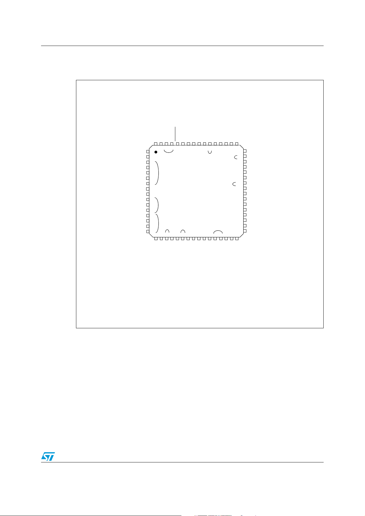
Figure 2. LQFP 64-pin package pinout . . . . . . . . . . . . . . . . . . . . . . . . . . . . . . . . . . . . . . . . . . . . . . . 21
Figure 3. LQFP 44-pin package pinout . . . . . . . . . . . . . . . . . . . . . . . . . . . . . . . . . . . . . . . . . . . . . . . 22
Figure 4. LQFP 32-pin package pinout . . . . . . . . . . . . . . . . . . . . . . . . . . . . . . . . . . . . . . . . . . . . . . . 23
Figure 5. Memory map . . . . . . . . . . . . . . . . . . . . . . . . . . . . . . . . . . . . . . . . . . . . . . . . . . . . . . . . . . . . 27
Figure 6. Memory map and sector address . . . . . . . . . . . . . . . . . . . . . . . . . . . . . . . . . . . . . . . . . . . . 31
Figure 7. Typical ICC interface . . . . . . . . . . . . . . . . . . . . . . . . . . . . . . . . . . . . . . . . . . . . . . . . . . . . . 32
Figure 8. CPU registers . . . . . . . . . . . . . . . . . . . . . . . . . . . . . . . . . . . . . . . . . . . . . . . . . . . . . . . . . . . 35
Figure 9. Stack manipulation example . . . . . . . . . . . . . . . . . . . . . . . . . . . . . . . . . . . . . . . . . . . . . . . . 38
Figure 10. PLL block diagram . . . . . . . . . . . . . . . . . . . . . . . . . . . . . . . . . . . . . . . . . . . . . . . . . . . . . . . 39
Figure 11. Clock, reset and supply block diagram . . . . . . . . . . . . . . . . . . . . . . . . . . . . . . . . . . . . . . . . 40
Figure 12. RESET sequence phases. . . . . . . . . . . . . . . . . . . . . . . . . . . . . . . . . . . . . . . . . . . . . . . . . . 42
Figure 13. Reset block diagram . . . . . . . . . . . . . . . . . . . . . . . . . . . . . . . . . . . . . . . . . . . . . . . . . . . . . 42
Figure 14. Reset sequences . . . . . . . . . . . . . . . . . . . . . . . . . . . . . . . . . . . . . . . . . . . . . . . . . . . . . . . . 43
Figure 15. Low voltage detector vs reset . . . . . . . . . . . . . . . . . . . . . . . . . . . . . . . . . . . . . . . . . . . . . . 44
Figure 16. Using the AVD to monitor VDD . . . . . . . . . . . . . . . . . . . . . . . . . . . . . . . . . . . . . . . . . . . . . 45
Figure 17. Interrupt processing flowchart . . . . . . . . . . . . . . . . . . . . . . . . . . . . . . . . . . . . . . . . . . . . . . 49
Figure 18. Priority decision process . . . . . . . . . . . . . . . . . . . . . . . . . . . . . . . . . . . . . . . . . . . . . . . . . . 49
Figure 19. Concurrent interrupt management . . . . . . . . . . . . . . . . . . . . . . . . . . . . . . . . . . . . . . . . . . . 51
Figure 20. Nested interrupt management . . . . . . . . . . . . . . . . . . . . . . . . . . . . . . . . . . . . . . . . . . . . . . 52
Figure 21. External interrupt control bits . . . . . . . . . . . . . . . . . . . . . . . . . . . . . . . . . . . . . . . . . . . . . . . 57
Figure 22. Power saving mode transitions . . . . . . . . . . . . . . . . . . . . . . . . . . . . . . . . . . . . . . . . . . . . . . 61
Figure 23. SLOW mode clock transitions. . . . . . . . . . . . . . . . . . . . . . . . . . . . . . . . . . . . . . . . . . . . . . . 62
Figure 24. WAIT mode flow-chart . . . . . . . . . . . . . . . . . . . . . . . . . . . . . . . . . . . . . . . . . . . . . . . . . . . . 63
Figure 25. HALT timing overview . . . . . . . . . . . . . . . . . . . . . . . . . . . . . . . . . . . . . . . . . . . . . . . . . . . . . 64
Figure 26. HALT mode flow-chart . . . . . . . . . . . . . . . . . . . . . . . . . . . . . . . . . . . . . . . . . . . . . . . . . . . . 64
Figure 27. ACTIVE HALT timing overview . . . . . . . . . . . . . . . . . . . . . . . . . . . . . . . . . . . . . . . . . . . . . . 66
Figure 28. ACTIVE HALT mode flow-chart . . . . . . . . . . . . . . . . . . . . . . . . . . . . . . . . . . . . . . . . . . . . . 66
Figure 29. AWUFH mode block diagram . . . . . . . . . . . . . . . . . . . . . . . . . . . . . . . . . . . . . . . . . . . . . . . 67
Figure 30. AWUF halt timing diagram . . . . . . . . . . . . . . . . . . . . . . . . . . . . . . . . . . . . . . . . . . . . . . . . . 68
Figure 31. AWUFH mode flow-chart . . . . . . . . . . . . . . . . . . . . . . . . . . . . . . . . . . . . . . . . . . . . . . . . . . 68
Figure 32. I/O port general block diagram . . . . . . . . . . . . . . . . . . . . . . . . . . . . . . . . . . . . . . . . . . . . . . 73
Figure 33. Interrupt I/O port state transitions . . . . . . . . . . . . . . . . . . . . . . . . . . . . . . . . . . . . . . . . . . . 75
Figure 34. Watchdog block diagram . . . . . . . . . . . . . . . . . . . . . . . . . . . . . . . . . . . . . . . . . . . . . . . . . . 81
Figure 35. Approximate timeout duration . . . . . . . . . . . . . . . . . . . . . . . . . . . . . . . . . . . . . . . . . . . . . . . 82
Figure 36. Exact timeout duration (tmin and tmax) . . . . . . . . . . . . . . . . . . . . . . . . . . . . . . . . . . . . . . . 83
Figure 37. Window watchdog timing diagram . . . . . . . . . . . . . . . . . . . . . . . . . . . . . . . . . . . . . . . . . . . 84
Figure 38. Main clock controller (MCC/RTC) block diagram . . . . . . . . . . . . . . . . . . . . . . . . . . . . . . . . 87
Figure 39. PWM auto-reload timer block diagram . . . . . . . . . . . . . . . . . . . . . . . . . . . . . . . . . . . . . . . . 91
Figure 40. Output compare control . . . . . . . . . . . . . . . . . . . . . . . . . . . . . . . . . . . . . . . . . . . . . . . . . . . 93
Figure 41. PWM auto-reload timer function . . . . . . . . . . . . . . . . . . . . . . . . . . . . . . . . . . . . . . . . . . . . . 93
Figure 42. PWM signal from 0% to 100% duty cycle . . . . . . . . . . . . . . . . . . . . . . . . . . . . . . . . . . . . . . 94
Figure 43. External event detector example (3 counts) . . . . . . . . . . . . . . . . . . . . . . . . . . . . . . . . . . . . 94
Figure 44. Input capture timing diagram, fCOUNTER = fCPU. . . . . . . . . . . . . . . . . . . . . . . . . . . . . . . 95
Figure 45. Input capture timing diagram, fCOUNTER = fCPU / 4 . . . . . . . . . . . . . . . . . . . . . . . . . . . . 96
Figure 46. ART external interrupt in halt mode . . . . . . . . . . . . . . . . . . . . . . . . . . . . . . . . . . . . . . . . . . 96
Figure 47. Timer block diagram . . . . . . . . . . . . . . . . . . . . . . . . . . . . . . . . . . . . . . . . . . . . . . . . . . . . . 104
Figure 48. 16-bit read sequence: (from counter or alternate counter register) . . . . . . . . . . . . . . . . . 104
16/279 Doc ID 12468 Rev 3

ST72361xx-Auto List of figures
Figure 49. Counter timing diagram, internal clock divided by 2 . . . . . . . . . . . . . . . . . . . . . . . . . . . . . 106
Figure 50. Counter timing diagram, internal clock divided by 4 . . . . . . . . . . . . . . . . . . . . . . . . . . . . . 106
Figure 51. Counter timing diagram, internal clock divided by 8 . . . . . . . . . . . . . . . . . . . . . . . . . . . . . 106
Figure 52. Input capture block diagram . . . . . . . . . . . . . . . . . . . . . . . . . . . . . . . . . . . . . . . . . . . . . . . 108
Figure 53. Input capture timing diagram . . . . . . . . . . . . . . . . . . . . . . . . . . . . . . . . . . . . . . . . . . . . . . 108
Figure 54. Output compare block diagram . . . . . . . . . . . . . . . . . . . . . . . . . . . . . . . . . . . . . . . . . . . . 110
Figure 55. Output compare timing diagram, fTIMER = fCPU/2 . . . . . . . . . . . . . . . . . . . . . . . . . . . . . 111
Figure 56. Output compare timing diagram, fTIMER = fCPU/4 . . . . . . . . . . . . . . . . . . . . . . . . . . . . . 111
Figure 57. One pulse mode timing example . . . . . . . . . . . . . . . . . . . . . . . . . . . . . . . . . . . . . . . . . . . 113
Figure 58. Pulse width modulation mode timing example with 2 output compare functions . . . . . . . 113
Figure 59. Timer block diagram . . . . . . . . . . . . . . . . . . . . . . . . . . . . . . . . . . . . . . . . . . . . . . . . . . . . . 126
Figure 60. Counter timing diagram, internal clock divided by 2 . . . . . . . . . . . . . . . . . . . . . . . . . . . . . 127
Figure 61. Counter timing diagram, internal clock divided by 4 . . . . . . . . . . . . . . . . . . . . . . . . . . . . . 127
Figure 62. Counter timing diagram, internal clock divided by 8 . . . . . . . . . . . . . . . . . . . . . . . . . . . . . 127
Figure 63. Input capture block diagram . . . . . . . . . . . . . . . . . . . . . . . . . . . . . . . . . . . . . . . . . . . . . . . 129
Figure 64. Input capture timing diagram . . . . . . . . . . . . . . . . . . . . . . . . . . . . . . . . . . . . . . . . . . . . . . 129
Figure 65. Output compare block diagram . . . . . . . . . . . . . . . . . . . . . . . . . . . . . . . . . . . . . . . . . . . . 131
Figure 66. Output compare timing diagram, fTIMER = fCPU/2 . . . . . . . . . . . . . . . . . . . . . . . . . . . . . 131
Figure 67. Output compare timing diagram, fTIMER = fCPU/4 . . . . . . . . . . . . . . . . . . . . . . . . . . . . . 132
Figure 68. One pulse mode timing example . . . . . . . . . . . . . . . . . . . . . . . . . . . . . . . . . . . . . . . . . . . 134
Figure 69. Pulse width modulation mode timing example . . . . . . . . . . . . . . . . . . . . . . . . . . . . . . . . . 134
Figure 70. Serial peripheral interface block diagram . . . . . . . . . . . . . . . . . . . . . . . . . . . . . . . . . . . . . 144
Figure 71. Single master/ single slave application. . . . . . . . . . . . . . . . . . . . . . . . . . . . . . . . . . . . . . . 145
Figure 72. Generic SS timing diagram . . . . . . . . . . . . . . . . . . . . . . . . . . . . . . . . . . . . . . . . . . . . . . . . 145
Figure 73. Hardware/software slave select management . . . . . . . . . . . . . . . . . . . . . . . . . . . . . . . . . 146
Figure 74. Data clock timing diagram . . . . . . . . . . . . . . . . . . . . . . . . . . . . . . . . . . . . . . . . . . . . . . . . 148
Figure 75. Clearing the WCOL bit (write collision flag) software sequence . . . . . . . . . . . . . . . . . . . . 150
Figure 76. Single master / multiple slave configuration . . . . . . . . . . . . . . . . . . . . . . . . . . . . . . . . . . . 151
Figure 77. SCI block diagram (in conventional baud rate generator mode). . . . . . . . . . . . . . . . . . . . 158
Figure 78. Word length programming . . . . . . . . . . . . . . . . . . . . . . . . . . . . . . . . . . . . . . . . . . . . . . . . 159
Figure 79. SCI baud rate and extended prescaler block diagram . . . . . . . . . . . . . . . . . . . . . . . . . . . 164
Figure 80. LIN characters . . . . . . . . . . . . . . . . . . . . . . . . . . . . . . . . . . . . . . . . . . . . . . . . . . . . . . . . . 174
Figure 81. SCI block diagram in LIN slave mode. . . . . . . . . . . . . . . . . . . . . . . . . . . . . . . . . . . . . . . . 175
Figure 82. LIN header reception timeout . . . . . . . . . . . . . . . . . . . . . . . . . . . . . . . . . . . . . . . . . . . . . . 178
Figure 83. LIN synch field measurement . . . . . . . . . . . . . . . . . . . . . . . . . . . . . . . . . . . . . . . . . . . . . . 179
Figure 84. LDIV read / write operations when LDUM = 0 . . . . . . . . . . . . . . . . . . . . . . . . . . . . . . . . . 181
Figure 85. LDIV read / write operations when LDUM = 1 . . . . . . . . . . . . . . . . . . . . . . . . . . . . . . . . . 181
Figure 86. Bit sampling in reception mode. . . . . . . . . . . . . . . . . . . . . . . . . . . . . . . . . . . . . . . . . . . . . 182
Figure 87. LSF bit set and clear . . . . . . . . . . . . . . . . . . . . . . . . . . . . . . . . . . . . . . . . . . . . . . . . . . . . . 187
Figure 88. SCI block diagram . . . . . . . . . . . . . . . . . . . . . . . . . . . . . . . . . . . . . . . . . . . . . . . . . . . . . . 195
Figure 89. Word length programming . . . . . . . . . . . . . . . . . . . . . . . . . . . . . . . . . . . . . . . . . . . . . . . . 196
Figure 90. SCI baud rate and extended prescaler block diagram . . . . . . . . . . . . . . . . . . . . . . . . . . . 200
Figure 91. SCI example of synchronous and asynchronous transmission . . . . . . . . . . . . . . . . . . . . 204
Figure 92. SCI data clock timing diagram (M = 0) . . . . . . . . . . . . . . . . . . . . . . . . . . . . . . . . . . . . . . . 204
Figure 93. SCI data clock timing diagram (M = 1) . . . . . . . . . . . . . . . . . . . . . . . . . . . . . . . . . . . . . . . 205
Figure 94. ADC block diagram . . . . . . . . . . . . . . . . . . . . . . . . . . . . . . . . . . . . . . . . . . . . . . . . . . . . . . 215
Figure 95. Pin loading conditions . . . . . . . . . . . . . . . . . . . . . . . . . . . . . . . . . . . . . . . . . . . . . . . . . . . . 227
Figure 96. Pin input voltage . . . . . . . . . . . . . . . . . . . . . . . . . . . . . . . . . . . . . . . . . . . . . . . . . . . . . . . . 228
Figure 97. fCPU maximum vs V
. . . . . . . . . . . . . . . . . . . . . . . . . . . . . . . . . . . . . . . . . . . . . . . . . . 230
DD
Figure 98. LVD startup behavior . . . . . . . . . . . . . . . . . . . . . . . . . . . . . . . . . . . . . . . . . . . . . . . . . . . . 231
Figure 99. Typical application with an external clock source . . . . . . . . . . . . . . . . . . . . . . . . . . . . . . . 234
Figure 100. Typical application with a crystal or ceramic resonator. . . . . . . . . . . . . . . . . . . . . . . . . . . 235
Doc ID 12468 Rev 3 17/279

List of figures ST72361xx-Auto
Figure 101. PLL jitter vs signal frequency
(1)
. . . . . . . . . . . . . . . . . . . . . . . . . . . . . . . . . . . . . . . . . . . . 236
Figure 102. AWU oscillator freq. @ TA 25°C. . . . . . . . . . . . . . . . . . . . . . . . . . . . . . . . . . . . . . . . . . . . 237
Figure 103. Connecting unused I/O pins . . . . . . . . . . . . . . . . . . . . . . . . . . . . . . . . . . . . . . . . . . . . . . . 242
Figure 104. RPU vs VDD with VIN = VSS . . . . . . . . . . . . . . . . . . . . . . . . . . . . . . . . . . . . . . . . . . . . . . 242
Figure 105. IPU vs VDD with VIN = VSS . . . . . . . . . . . . . . . . . . . . . . . . . . . . . . . . . . . . . . . . . . . . . . . 242
Figure 106. Typical VOL at VDD = 5V (standard) . . . . . . . . . . . . . . . . . . . . . . . . . . . . . . . . . . . . . . . . 243
Figure 107. Typical VOL at VDD = 5V (high-sink) . . . . . . . . . . . . . . . . . . . . . . . . . . . . . . . . . . . . . . . . 243
Figure 108. Typical VOH at VDD = 5V. . . . . . . . . . . . . . . . . . . . . . . . . . . . . . . . . . . . . . . . . . . . . . . . . 244
Figure 109. Typical VOL vs VDD (standard I/Os) . . . . . . . . . . . . . . . . . . . . . . . . . . . . . . . . . . . . . . . . 244
Figure 110. Typical VOL vs VDD (high-sink I/Os) . . . . . . . . . . . . . . . . . . . . . . . . . . . . . . . . . . . . . . . . 244
Figure 111. Typical VOH vs VDD . . . . . . . . . . . . . . . . . . . . . . . . . . . . . . . . . . . . . . . . . . . . . . . . . . . . 245
Figure 112. RESET pin protection when LVD is disabled . . . . . . . . . . . . . . . . . . . . . . . . . . . . . . . . . . 246
Figure 113. RESET pin protection when LVD is enabled . . . . . . . . . . . . . . . . . . . . . . . . . . . . . . . . . . 246
Figure 114. RESET
RPU vs VDD . . . . . . . . . . . . . . . . . . . . . . . . . . . . . . . . . . . . . . . . . . . . . . . . . . . . 247
Figure 115. Two typical applications with ICCSEL/VPP pin . . . . . . . . . . . . . . . . . . . . . . . . . . . . . . . . 247
Figure 116. SPI slave timing diagram with CPHA = 0 . . . . . . . . . . . . . . . . . . . . . . . . . . . . . . . . . . . . . 251
Figure 117. SPI slave timing diagram with CPHA = 1 . . . . . . . . . . . . . . . . . . . . . . . . . . . . . . . . . . . . . 251
Figure 118. SPI master timing diagram . . . . . . . . . . . . . . . . . . . . . . . . . . . . . . . . . . . . . . . . . . . . . . . . 252
Figure 119. RAIN max vs fADC with CAIN = 0pF . . . . . . . . . . . . . . . . . . . . . . . . . . . . . . . . . . . . . . . . 253
Figure 120. Recommended CAIN/RAIN values . . . . . . . . . . . . . . . . . . . . . . . . . . . . . . . . . . . . . . . . . . 253
Figure 121. Typical application with ADC . . . . . . . . . . . . . . . . . . . . . . . . . . . . . . . . . . . . . . . . . . . . . . 253
Figure 122. Power supply filtering . . . . . . . . . . . . . . . . . . . . . . . . . . . . . . . . . . . . . . . . . . . . . . . . . . . . 254
Figure 123. ADC accuracy . . . . . . . . . . . . . . . . . . . . . . . . . . . . . . . . . . . . . . . . . . . . . . . . . . . . . . . . . 256
Figure 124. 32-pin low profile quad flat package (7x7) . . . . . . . . . . . . . . . . . . . . . . . . . . . . . . . . . . . . 257
Figure 125. 44-pin low profile quad flat package (10x10) . . . . . . . . . . . . . . . . . . . . . . . . . . . . . . . . . . 258
Figure 126. 64-pin low profile quad flat package (10 x10) . . . . . . . . . . . . . . . . . . . . . . . . . . . . . . . . . . 258
Figure 127. pin 1 orientation in tape and reel conditioning . . . . . . . . . . . . . . . . . . . . . . . . . . . . . . . . . 259
Figure 128. ST72F361xx-Auto Flash commercial product structure . . . . . . . . . . . . . . . . . . . . . . . . . . 264
Figure 129. ST72P361xxx-Auto FastROM commercial product structure . . . . . . . . . . . . . . . . . . . . . . 265
Figure 130. ST72361xx-Auto ROM commercial product structure . . . . . . . . . . . . . . . . . . . . . . . . . . . 266
Figure 131. Header reception event sequence . . . . . . . . . . . . . . . . . . . . . . . . . . . . . . . . . . . . . . . . . . 273
Figure 132. LINSCI interrupt routine . . . . . . . . . . . . . . . . . . . . . . . . . . . . . . . . . . . . . . . . . . . . . . . . . . 273
18/279 Doc ID 12468 Rev 3

ST72361xx-Auto Description
1 Description
The ST72361xx-Auto devices are members of the ST7 microcontroller family designed for
automotive mid-range applications with LIN (Local Interconnect Network) interface.
All devices are based on a common industry-standard 8-bit core, featuring an enhanced
instruction set and are available with Flash or ROM program memory.
The enhanced instruction set and addressing modes of the ST7 offer both power and
flexibility to software developers, enabling the design of highly efficient and compact
application code. In addition to standard 8-bit data management, all ST7 microcontrollers
feature true bit manipulation, 8x8 unsigned multiplication and indirect addressing modes.
Table 2. Product overview
Features ST72361(AR/J/K)9 ST7261(AR/J/K)7 ST72361(AR/J/K)6 ST72361(AR/J/K)4
Program memory -
bytes
RAM (stack) - bytes 2K (256) 2K (256) 1.5K (256) 1.5K (256)
Operating supply 4.5V to 5.5V
CPU frequency External resonator oscillator w/ PLLx2/8 MHz
Maximum
temperature range
Packages LQFP64 10x10mm (AR), LQFP44 10x10mm (J), LQFP32 7x7mm (K)
1. FASTROM and ROM versions only.
60K 48K
(1)
-40°C to +125°C
32K 16K
Doc ID 12468 Rev 3 19/279
Description ST72361xx-Auto
8-BIT CORE
ALU
ADDRESS AND DATA BUS
OSC1
OSC2
RESET
PORT A
CONTROL
RAM
PA7:0
(8 bits)
1
PROGRAM
(16 - 60 Kbytes)
MEMORY
PLL x 2
PWM
8-Bit
PORT B
PORT C
SPI
LINSCI2
PB7:0
(8 bits)
1
PC7:0
(8 bits)
1
OSC
PORT D
PD7:0
(8 bits)
1
/2
option
LINSCI1
16-Bit
TIMER
(LIN master)
(LIN master/slave)
V
SS
V
DD
POWER
SUPPLY
PORT E
PE7:0
(8 bits)
1
PORT F
PF7:0
(8 bits)
1
TIMER
ART
MCC
(Clock Control)
TLI
1
WATCHDOG
WINDOW
(1.5 - 2 Kbytes)
Figure 1. Device block diagram
1. On some devices only (see Table 2: Product overview)
20/279 Doc ID 12468 Rev 3
ST72361xx-Auto Description
AIN15 / PE3
ICCDATA / AIN1 / PB5
(*)T16_OCMP1 / AIN2 / PB6
V
SS_2
V
DD_2
(*)T16_OCMP2 / AIN3 / PB7
(*)T16_ICAP1 / AIN4 / PC0
(*)T16_ICAP2 / (HS) PC1
T16_EXTCLK / (HS) PC2
PE4
NC
ICCSEL/V
PP
AIN12 / PE0
AIN13 / PE1
ICCCLK / AIN0 / PB4
AIN14 / PE2
64 63 62 61 60 59 58 57 56 55 54 53 52 51 50 49
48
47
46
45
44
43
42
41
40
39
38
37
36
35
34
33
17 18 19 20 21 22 23 24 29 30 31 3225 26 27 28
1
2
3
4
5
6
7
8
9
10
11
12
13
14
15
16
PWM1 / (HS) PA2
PWM2 / PA3
PWM3 / PA4
V
SS_3
V
DD_3
ARTCLK / (HS)PA5
ARTIC2 / (HS) PA6
T8_OCMP2 / PA7
T8_ICAP2 / PB0
T8_OCMP1 / PB1
T8_ICAP1 / PB2
MCO / PB3
OSC1
OSC2
ARTIC1 / PA0
PWM0 / PA1
PF0
PE7
PD0 / SPI_SS / AIN6
V
DD_1
V
SS_1
PC7 / SPI_SCK
PC6 / SPI_MOSI
PC5 / SPI_MISO
PE6 / AIN5
PE5
PC4
PC3
PD2 / LINSCI1_TDO
PD1 / LINSCI1_RDI
PF2 / AIN8
PF1 / AIN7
RESET
PD5 / LINSCI2_TDO
V
DD_0VDDAVSS_0VSSA
PD4 / LINSCI2_RDI
PD3 (HS)/ LINSCI2_SCK
PF5
TLI
PF4
PF3 / AIN9
PF7
PF6
PD7 / AIN11
PD6 / AIN10
ei0
(HS) 20mA high sink capability
eix associated external interrupt vector
ei3
ei1
ei1
ei3
ei3
ei2
ei3
ei0
ei1
(*) : by option bit:
T16_ICAP2 can be moved to PD1
T16_OCMP1 can be moved to PD3
T16_OCMP2 can be moved to PD5
T16_ICAP1 can be moved to PD4
1.1 Pin description
Figure 2. LQFP 64-pin package pinout
Doc ID 12468 Rev 3 21/279
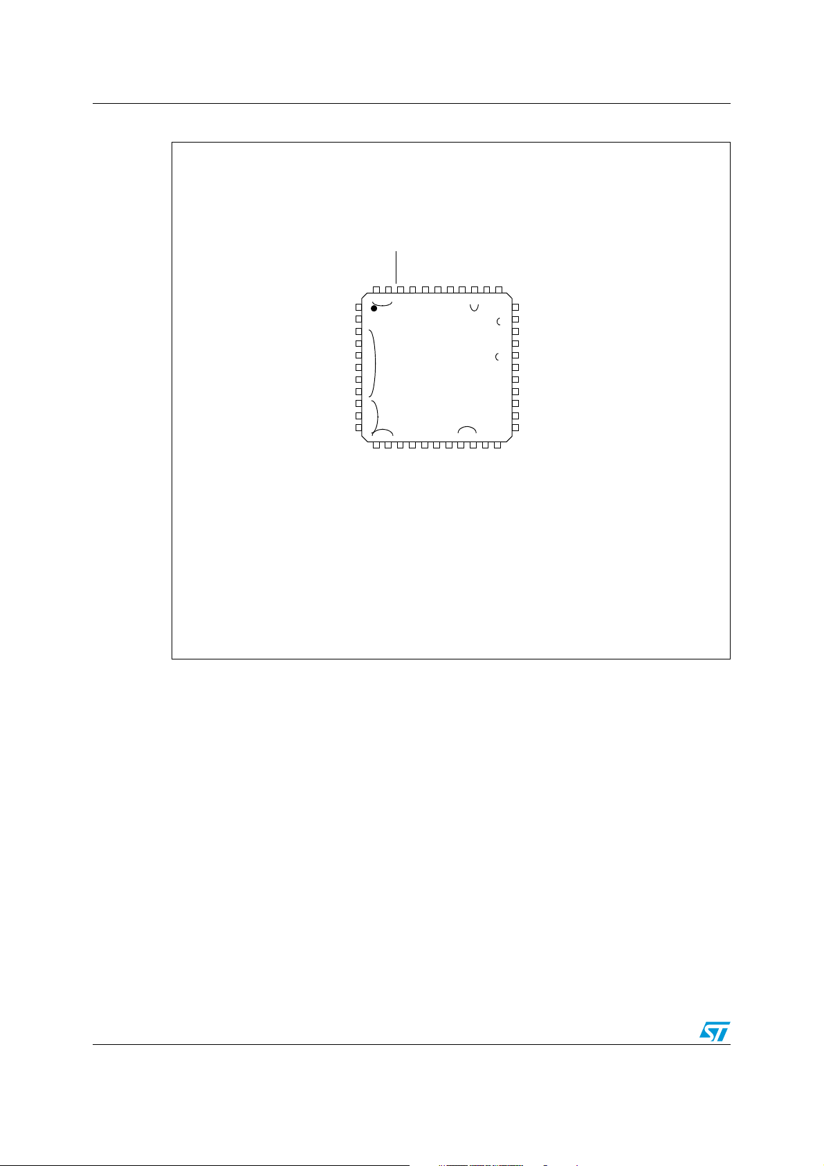
Description ST72361xx-Auto
V
SS_2
V
DD_2
(*)T16_OCMP2 / AIN3 / PB7
(*)T16_ICAP1 / AIN4 / PC0
(*)T16_ICAP2 / (HS) PC1
T16_EXTCLK / (HS) PC2
PE4
ICCSEL/VPP
ICCCLK / AIN0 / PB4
ICCDATA / AIN1 / PB5
(*)T16_OCMP1 / AIN2 / PB6
44 43 42 41 40 39 38 37 36 35 34
33
32
31
30
29
28
27
26
25
24
23
12 13 14 15 16 17 18 19 20 21 22
1
2
3
4
5
6
7
8
9
10
11
PWM2 / PA3
PWM3 / PA4
ARTCLK / (HS)PA5
ARTIC2 / (HS) PA6
T8_OCMP1 / PB1
T8_ICAP1 / PB2
MCO / PB3
OSC1
OSC2
PWM0 / PA1
PWM1 / (HS) PA2
PD0 / SPI_SS / AIN6
PC7 / SPI_SCK
PC6 / SPI_MOSI
PC5 / SPI_MISO
PE6 / AIN5
PC4
PC3
PD2 / LINSCI1_TDO
PD1 / LINSCI1_RDI
PF2 / AIN8
PF1 / AIN7
V
DD_0VDDAVSS_0VSSA
PD4 / LINSCI2_RDI
PD3 (HS) / LINSCI2_SCK
PF5
PD7 / AIN11
PD6 / AIN10
RESET
PD5 / LINSCI2_TDO
1
(HS) 20mA high sink capability
eix associated external interrupt vector
ei0
ei3
ei3
ei1
ei3
ei1
ei2
ei3
(*) : by option bit:
T16_ICAP2 can be moved to PD1
T16_OCMP1 can be moved to PD3
T16_OCMP2 can be moved to PD5
T16_ICAP1 can be moved to PD4
Figure 3. LQFP 44-pin package pinout
22/279 Doc ID 12468 Rev 3

ST72361xx-Auto Description
T16_OCMP2 / AIN3 / PB7
T16_ICAP1 / AIN4 / PC0
T16_ICAP2 / (HS) PC1
T16_EXTCLK / (HS) PC2
ICCSEL/V
PP
ICCCLK / AIN0 / PB4
ICCDATA / AIN1 / PB5
T16_OCMP1 / AIN2 / PB6
32 31 30 29 28 27 26 25
24
23
22
21
20
19
18
17
9 101112131415
16
1
2
3
4
5
6
7
8
ARTCLK / (HS) PA5
T8_OCMP1 / PB1
T8_ICAP1 / PB2
MCO / PB3
OSC1
OSC2
PWM0 / PA1
PWM1 / (HS) PA2
PC6 / SPI_MOSI
PC5 / SPI_MISO
PC4
PC3
PD2 / LINSCI1_TDO
PD1 / LINSCI1_RDI
PD0 / SPI_SS / AIN6
PC7 / SPI_SCK
V
SS_0VSSA
PD4 / LINSCI2_RDI
PD3 (HS) / LINSCI2_SCK
1
RESET
PD5 / LINSCI2_TDO
V
DD_0VDDA
(HS) 20mA high sink capability
eix associated external interrupt vector
ei0
ei1
ei3
ei3
ei1
ei2
(*) : by option bit:
T16_ICAP2 can be moved to PD1
T16_OCMP1 can be moved to PD3
T16_OCMP2 can be moved to PD5
T16_ICAP1 can be moved to PD4
Figure 4. LQFP 32-pin package pinout
For external pin connection guidelines, refer to Chapter 20: Electrical characteristics.
Doc ID 12468 Rev 3 23/279
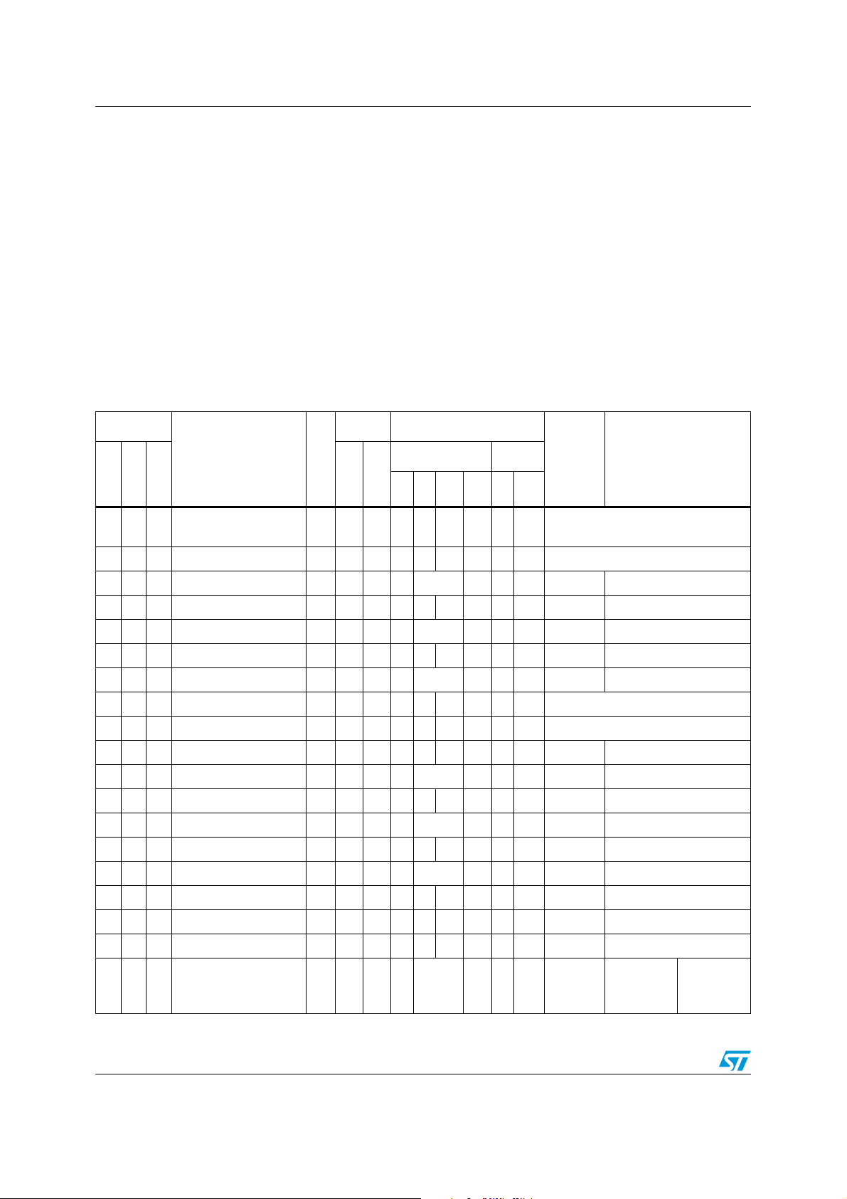
Description ST72361xx-Auto
List of abbreviations used in Tab l e 3
Type: I = input, O = output, S = supply
In/Output level: C
= CMOS 0.3VDD/0.7VDD with Schmitt trigger
T
T
= TTL 0.8V / 2V with Schmitt trigger
T
Output level: HS = 20mA high sink (on N-buffer only)
Port and control configuration:
Input: float = floating, wpu = weak pull-up, int = interrupt, ana = analog,
RB = robust
Output: OD = open drain, PP = push-pull
Refer to Chapter 8: I/O ports for more details on the software configuration of the I/O ports.
The RESET configuration of each pin is shown in bold which is valid as long as the device is
in reset state.
LQFP44
LQFP32
SS_3
DD_3
Pin name
(2)
(2)
Type
I
I/O Resonator oscillator inverter output
S Digital ground voltage
S Digital main supply voltage
Table 3. Device pin description
Pin n°
LQFP64
111OSC1
222OSC2
3 - - PA0 / ARTIC1 I/O C
4 3 3 PA1 / PWM0 I/O C
5 4 4 PA2 (HS) / PWM1 I/O C
6 5 - PA3 / PWM2 I/O C
7 6 - PA4 / PWM3 I/O C
8--V
9--V
10 7 5 PA5 (HS) / ARTCLK I/O C
11 8 - PA6 (HS) / ARTIC2 I/O C
12 - - PA7 / T8_OCMP2 I/O C
13 - - PB0 /T8_ICAP2 I/O C
14 9 6 PB1 /T8_OCMP1 I/O C
15 10 7 PB2 / T8_ICAP1 I/O C
16 11 8 PB3 / MCO I/O C
17 - - PE0 / AIN12 I/O T
18 - - PE1 / AIN13 I/O T
19 12 9 PB4 / AIN0 / ICCCLK I/O C
Level Port
(1)
Input
Input
Output
float
int
wpu
Output
ana
OD
function
PP
Main
(after
reset)
Alternate function
External clock input or resonator
oscillator inverter input
T
T
T
T
T
T
T
T
T
T
T
T
T
T
T
X ei0 X X Port A0 ART input capture 1
X ei0 X X Port A1 ART PWM output 0
HS X ei0 X X Port A2 ART PWM output 1
X ei0 X X Port A3 ART PWM output 2
X ei0 X X Port A4 ART PWM output 3
HS X ei0 X X Port A5 ART external clock
HS X ei0 X X Port A6 ART input capture 2
X ei0 X X Port A7 TIM8 output capture 2
X ei1 X X Port B0 TIM8 input capture 2
X ei1 X X Port B1 TIM8 output capture 1
X ei1 X X Port B2 TIM8 input capture 1
X ei1 X X Port B3 Main clock out (f
X X RB X X Port E0 ADC analog input 12
X X RB X X Port E1 ADC analog input 13
X ei1 RB X X Port B4
ICC clock
input
OSC2
ADC
analog
input 0
)
24/279 Doc ID 12468 Rev 3

ST72361xx-Auto Description
Table 3. Device pin description (continued)
Pin n°
Pin name
LQFP64
LQFP44
LQFP32
20 - - PE2 / AIN14 I/O T
21 - - PE3 / AIN15 I/O T
22 13 10 PB5 / AIN1 / ICCDATA I/O C
23 14 11
24 15 - V
25 16 - V
26 17 12
27 18 13
28 19 14
29 20 15
PB6 / AIN2 /
T16_OCMP1
SS_2
DD_2
PB7 /AIN3 /
T16_OCMP2
PC0 / AIN4 /
T16_ICAP1
PC1 (HS) /
T16_ICAP2
PC2 (HS) /
T16_EXTCLK
30 21 - PE4 I/O T
Level Port
Type
I/O C
(1)
Input
Input
Output
float
T
T
T
T
X X RB X X Port E2 ADC analog input 14
X X RB X X Port E3 ADC analog input 15
Xei1RBXXPort B5
XX RBX X Port B6
int
wpu
Output
ana
OD
function
PP
(after
reset)
S Digital ground voltage
S Digital main supply voltage
I/O C
I/O C
T
T
XX RBX X Port B7
XX RBX X Port C0
I/O CTHS X ei2 X X Port C1 TIM16 input capture 2
I/O C
HS X ei2 X X Port C2
T
T
XX X X Port E4
31 - - NC Not Connected
Main
Alternate function
ICC data
input
TIM16
output
compare 1
TIM16
output
compare 2
TIM16
input
capture 1
ADC
analog
input 1
ADC
analog
input 2
ADC
analog
input 3
ADC
analog
input 4
TIM16 external clock
input
32 22 16 V
PP
I
33 23 17 PC3 I/O C
34 24 18 PC4 I/O C
35 - - PE5 I/O T
36 25 - PE6 / AIN5 I/O T
37 26 19 PC5 /MISO I/O C
38 27 20 PC6 / MOSI I/O C
39 28 21 PC7 /SCK I/O C
40 - - V
41 - - V
SS_1
DD_1
42 29 22 PD0 / SS
/ AIN6 I/O C
S Digital ground voltage
S Digital main supply voltage
43 - - PE7 I/O T
Flash programming voltage.Must
be tied low in user mode
T
T
T
T
T
T
T
T
T
XX X X Port C3
XX
(3)
Por t C4
XX X X Port E5
X X X X X Port E6 ADC analog input 5
X X X X Port C5 SPI master in/slave out
X X X X Port C6 SPI master out/slave in
X X X X Port C7 SPI serial clock
ADC
analog
input 6
Xei3 XXXPort D0
SPI slave
select
XX X X Port E7
Doc ID 12468 Rev 3 25/279
Description ST72361xx-Auto
Table 3. Device pin description (continued)
Pin n°
Pin name
LQFP64
LQFP44
LQFP32
44 - - PF0 I/O T
45 30 - PF1 / AIN7 I/O T
46 31 - PF2 / AIN8 I/O T
47 32 23 PD1 / SCI1_RDI I/O C
48 33 24 PD2 / SCI1_TDO I/O C
49 - - PF3 / AIN9 I/O T
50 - - PF4 I/O T
51 - - TLI I C
52 34 - PF5 I/O T
53 35 25 PD3 (HS) / SCI2_SCK I/O CTHS X X X X Port D3
54 36 26 PD4 / SCI2_RDI I/O C
55 37 27 V
56 38 28 V
57 39 29 V
58 40 30 V
SSA
SS_0
DDA
DD_0
59 41 31 PD5 / SCI2_TDO I/O C
60 42 32 RESET I/O C
61 43 - PD6 / AIN10 I/O C
62 44 - PD7 / AIN11 I/O C
63 - - PF6 I/O T
64 - - PF7 I/O T
1. In the interrupt input column, “eiX” defines the associated external interrupt vector. If the weak pull-up column (wpu) is
merged with the interrupt column (int), then the I/O configuration is pull-up interrupt input, else the configuration is floating
interrupt input.
2. OSC1 and OSC2 pins connect a crystal/ceramic resonator, or an external source to the on-chip oscillator; see Chapter 1: Description and
Section 20.5: Clock and timing characteristics for more details.
3. Input mode can be used for general purpose I/O, output mode cannot be used.
On the chip, each I/O port has eight pads. Pads that are not bonded to external pins are in input pull-up configuration after
reset. The configuration of these pads must be kept at reset state to avoid added current consumption.
Level Port
Input
Type
Input
Output
float
T
T
T
T
T
T
T
T
T
XX X X Port F0
X X X X X Port F1 ADC analog input 7
X X X X X Port F2 ADC analog input 8
X ei3 X X Port D1
XX X X Port D2
X X X X X Port F3 ADC analog input 9
XX X X Port F4
X X Top level interrupt input pin
XX X X Port F5
(1)
int
wpu
Output
ana
OD
function
PP
Main
(after
reset)
Alternate function
LINSCI1 receive data
input
LINSCI1 transmit data
output
LINSCI2 serial clock
output
T
X ei3 X X Port D4
LINSCI2 receive data
input
S Analog ground voltage
S Digital ground voltage
I Analog reference voltage for ADC
S Digital main supply voltage
T
T
T
T
T
T
XX X X Port D5
Top priority non maskable
interrupt.
X ei3 X X X Port D6 ADC analog input 10
X ei3 X X X Port D7 ADC analog input 11
XX X X Port F6
XX X X Port F7
LINSCI2 transmit data
output
26/279 Doc ID 12468 Rev 3
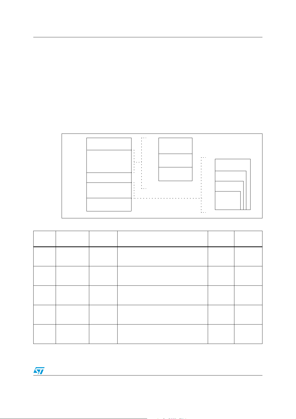
ST72361xx-Auto Register and memory map
0000h
RAM
Program Memory
(60K, 48K, 32K, 16K)
Interrupt & Reset Vectors
HW Registers
0080h
007Fh
0FFFh
(see Ta bl e 4)
1000h
FFDFh
FFE0h
FFFFh
(see Ta bl e 16 )
0880h
Reserved
087Fh
Short Addressing
RAM (zero page)
256 bytes Stack
16-bit Addressing
RAM
0100h
01FFh
0080h
0200h
00FFh
1000h
32 Kbytes
60 Kbytes
FFDFh
8000h
or 087Fh
16 Kbytes
C000h
48 Kbytes
4000h
(2048/1536 bytes)
067Fh
2 Register and memory map
As shown in Figure 5, the MCU is capable of addressing 64 Kbytes of memories and I/O
registers.
The available memory locations consist of 128 bytes of register locations, up to 2 Kbytes of
RAM and up to 60 Kbytes of user program memory.
The RAM space includes up to 256 bytes for the stack from 0100h to 01FFh.The highest
address bytes contain the user reset and interrupt vectors.
Caution: Memory locations marked as “Reserved” must never be accessed. Accessing a reserved
area can have unpredictable effects on the device.
Figure 5. Memory map
Table 4. Hardware register map
Address Block
0000h
0001h
0002h
0003h
0004h
0005h
0006h
0007h
0008h
0009h
000Ah
000Bh
000Ch
000Dh
000Eh
Por t A
Por t B
Por t C
Por t D
Por t E
Register
label
PA DR
PADDR
PA OR
PBDR
PBDDR
PBOR
PCDR
PCDDR
PCOR
PDDR
PDDDR
PDOR
PEDR
PEDDR
PEOR
Register name
Port A Data Register
Port A Data Direction Register
Port A Option Register
Port B Data Register
Port B Data Direction Register
Port B Option Register
Port C Data Register
Port C Data Direction Register
Port C Option Register
Port D Data Register
Port D Data Direction Register
Port D Option Register
Port E Data Register
Port E Data Direction Register
Port E Option Register
Doc ID 12468 Rev 3 27/279
Reset
status
(2)
00h
00h
00h
(2)
00h
00h
00h
(2)
00h
00h
00h
(2)
00h
00h
00h
(2)
00h
00h
00h
Remarks
(3)
R/W
(3)
R/W
(3)
R/W
(3)
R/W
(3)
R/W
(3)
R/W
(3)
R/W
(3)
R/W
(3)
R/W
(3)
R/W
(3)
R/W
(3)
R/W
(3)
R/W
(3)
R/W
(3)
R/W
(1)

Register and memory map ST72361xx-Auto
Table 4. Hardware register map (continued)
Address Block
000Fh
0010h
Por t F
0011h
Register
label
PFDR
PFDDR
PFOR
Register name
Port F Data Register
Port F Data Direction Register
Port F Option Register
Reset
status
(2)
00h
00h
00h
R/W
R/W
R/W
0012h
to
Reserved Area (15 bytes)
0020h
0021h
0022h
0023h
SPI
SPIDR
SPICR
SPICSR
SPI Data I/O Register
SPI Control Register
SPI Control/Status Register
xxh
0xh
00h
R/W
R/W
R/W
0024h FLASH FCSR Flash Control/Status Register 00h R/W
0025h
0026h
0027h
0028h
0029h
002Ah
002Bh
002Ch
002Dh
002Eh
ITC
AWU
CKCTRL
ISPR0
ISPR1
ISPR2
ISPR3
EICR0
EICR1
AWUCSR
AWUPR
SICSR
MCCSR
Interrupt Software Priority Register 0
Interrupt Software Priority Register 1
Interrupt Software Priority Register 2
Interrupt Software Priority Register 3
External Interrupt Control Register 0
External Interrupt Control Register 1
Auto Wake up f. Halt Control/Status Register
Auto Wake Up From Halt Prescaler
System Integrity Control / Status Register
Main Clock Control / Status Register
FFh
FFh
FFh
FFh
00h
00h
00h
FFh
0xh
00h
R/W
R/W
R/W
R/W
R/W
R/W
R/W
R/W
R/W
R/W
Remarks
(3)
(3)
(3)
(1)
002Fh
0030h
0031h
0032h
0033h
0034h
0035h
0036h
0037h
0038h
0039h
003Ah
003Bh
003Ch
003Dh
003Eh
003Fh
0040h
0041h
0042h
0043h
0044h
0045h
0046h
0047h
WWDG
PWM
ART
8-BIT
TIMER
ADC
WDGCR
WDGWR
PWMDCR3
PWMDCR2
PWMDCR1
PWMDCR0
PWMCR
ARTCSR
ARTCAR
ARTARR
ARTICCSR
ARTICR1
ARTICR2
T8CR2
T8CR1
T8CSR
T8IC1R
T8OC1R
T8CTR
T8ACTR
T8IC2R
T8OC2R
ADCCSR
ADCDRH
ADCDRL
Watchdog Control Register
Watchdog Window Register
Pulse Width Modulator Duty Cycle Register
3
PWM Duty Cycle Register 2
PWM Duty Cycle Register 1
PWM Duty Cycle Register 0
PWM Control register
Auto-Reload Timer Control/Status Register
Auto-Reload Timer Counter Access Register
Auto-Reload Timer Auto-Reload Register
ART Input Capture Control/Status Register
ART Input Capture Register 1
ART Input Capture register 2
Timer Control Register 2
Timer Control Register 1
Timer Control/Status Register
Timer Input Capture 1 Register
Timer Output Compare 1 Register
Timer Counter Register
Timer Alternate Counter Register
Timer Input Capture 2 Register
Timer Output Compare 2 Register
Control/Status Register
Data High Register
Data Low Register
7Fh
7Fh
00h
00h
00h
00h
00h
00h
00h
00h
00h
00h
00h
00h
00h
00h
xxh
00h
FCh
FCh
xxh
00h
00h
00h
00h
R/W
R/W
R/W
R/W
R/W
R/W
R/W
R/W
R/W
R/W
R/W
Read Only
Read Only
R/W
R/W
Read Only
Read Only
R/W
Read Only
Read Only
Read Only
R/W
R/W
Read Only
Read Only
28/279 Doc ID 12468 Rev 3

ST72361xx-Auto Register and memory map
Table 4. Hardware register map (continued)
Address Block
0048h
0049h
004Ah
004Bh
004Ch
004Dh
LINSCI1
(LIN
Master/Slave)
004Eh
004Fh
Register
label
SCI1ISR
SCI1DR
SCI1BRR
SCI1CR1
SCI1CR2
SCI1CR3
SCI1ERPR
SCI1ETPR
Register name
SCI1 Status Register
SCI1 Data Register
SCI1 Baud Rate Register
SCI1 Control Register 1
SCI1 Control Register 2
SCI1Control Register 3
SCI1 Extended Receive Prescaler Register
SCI1 Extended Transmit Prescaler Register
0050h Reserved Area (1 byte)
0051h
0052h
0053h
0054h
0055h
0056h
0057h
0058h
0059h
005Ah
005Bh
005Ch
005Dh
005Eh
005Fh
0060h
0061h
0062h
0063h
0064h
0065h
0066h
0067h
16-BIT
TIMER
LINSCI2
(LIN Master)
T16CR2
T16CR1
T16CSR
T16IC1HR
T16IC1LR
T16OC1HR
T16OC1LR
T16CHR
T16CLR
T16ACHR
T16ACLR
T16IC2HR
T16IC2LR
T16OC2HR
T16OC2LR
SCI2SR
SCI2DR
SCI2BRR
SCI2CR1
SCI2CR2
SCI2CR3
SCI2ERPR
SCI2ETPR
Timer Control Register 2
Timer Control Register 1
Timer Control/Status Register
Timer Input Capture 1 High Register
Timer Input Capture 1 Low Register
Timer Output Compare 1 High Register
Timer Output Compare 1 Low Register
Timer Counter High Register
Timer Counter Low Register
Timer Alternate Counter High Register
Timer Alternate Counter Low Register
Timer Input Capture 2 High Register
Timer Input Capture 2 Low Register
Timer Output Compare 2 High Register
Timer Output Compare 2 Low Register
SCI2 Status Register
SCI2 Data Register
SCI2 Baud Rate Register
SCI2 Control Register 1
SCI2 Control Register 2
SCI2 Control Register 3
SCI2 Extended Receive Prescaler Register
SCI2 Extended Transmit Prescaler Register
Reset
status
C0h
xxh
00h
xxh
00h
00h
00h
00h
00h
00h
00h
xxh
xxh
80h
00h
FFh
FCh
FFh
FCh
xxh
xxh
80h
00h
C0h
xxh
00h
xxh
00h
00h
00h
00h
Remarks
Read Only
R/W
R/W
R/W
R/W
R/W
R/W
R/W
R/W
R/W
R/W
Read Only
Read Only
R/W
R/W
Read Only
Read Only
Read Only
Read Only
Read Only
Read Only
R/W
R/W
Read Only
R/W
R/W
R/W
R/W
R/W
R/W
R/W
(1)
0068h
to
Reserved area (24 bytes)
007Fh
1. x = undefined, R/W = read/write
2. The contents of the I/O port DR registers are readable only in output configuration. In input configuration, the values of the
I/O pins are returned instead of the DR register contents.
3. The bits associated with unavailable pins must always keep their reset value.
Doc ID 12468 Rev 3 29/279

Flash program memory ST72361xx-Auto
3 Flash program memory
3.1 Introduction
The ST7 dual voltage High Density Flash (HDFlash) is a non-volatile memory that can be
electrically erased as a single block or by individual sectors and programmed on a Byte-byByte basis using an external V
The HDFlash devices can be programmed and erased off-board (plugged in a programming
tool) or on-board using ICP (In-Circuit Programming) or IAP (In-Application Programming).
The array matrix organization allows each sector to be erased and reprogrammed without
affecting other sectors.
3.2 Main features
● 3 Flash programming modes:
– Insertion in a programming tool. In this mode, all sectors including option bytes
can be programmed or erased.
– ICP (In-Circuit Programming). In this mode, all sectors including option bytes can
be programmed or erased without removing the device from the application board.
– IAP (In-Application Programming) In this mode, all sectors except Sector 0, can be
programmed or erased without removing the device from the application board
and while the application is running.
● ICT (In-Circuit Testing) for downloading and executing user application test patterns in
RAM
● Read-out protection
● Register Access Security System (RASS) to prevent accidental programming or
erasing
supply.
PP
3.3 Structure
The Flash memory is organized in sectors and can be used for both code and data storage.
Depending on the overall Flash memory size in the microcontroller device, there are up to
three user sectors (see Ta b l e 5 ). Each of these sectors can be erased independently to
avoid unnecessary erasing of the whole Flash memory when only a partial erasing is
required.
The first two sectors have a fixed size of 4 Kbytes (see Figure 6). They are mapped in the
upper part of the ST7 addressing space so the reset and interrupt vectors are located in
Sector 0 (F000h-FFFFh).
Table 5. Sectors available in Flash devices
Flash size (bytes) Available sectors
4K Sector 0
8K Sectors 0,1
> 8K Sectors 0,1, 2
30/279 Doc ID 12468 Rev 3

ST72361xx-Auto Flash program memory
4 Kbytes
4 Kbytes
2Kbytes
SECTOR 1
SECTOR 0
16 Kbytes
SECTOR 2
8K 16K 32K 60K
FLASH
FFFFh
EFFFh
DFFFh
3FFFh
7FFFh
1000h
24 Kbytes
MEMORY SIZE
8Kbytes 40 Kbytes
52 Kbytes
9FFFh
BFFFh
D7FFh
4K 10K 24K 48K
3.3.1 Read-out protection
Read-out protection, when selected, provides a protection against Program Memory content
extraction and against write access to Flash memory. Even if no protection can be
considered as totally unbreakable, the feature provides a very high level of protection for a
general purpose microcontroller.
In Flash devices, this protection is removed by reprogramming the option. In this case, the
entire program memory is first automatically erased and the device can be reprogrammed.
Read-out protection selection depends on the device type:
● In Flash devices it is enabled and removed through the FMP_R bit in the option byte.
● In ROM devices it is enabled by mask option specified in the Option List.
Figure 6. Memory map and sector address
3.4 ICC interface
ICC (In-Circuit Communication) needs a minimum of four and up to six pins to be connected
to the programming tool (see Figure 7). These pins are:
● RESET: device reset
● V
● ICCCLK: ICC output serial clock pin
● ICCDATA: ICC input/output serial data pin
● ICCSEL/V
● OSC1(or OSCIN): main clock input for external source (optional)
● V
: device power supply ground
SS
: programming voltage
PP
: application board power supply (see Figure 7, Note 3)
DD
Doc ID 12468 Rev 3 31/279
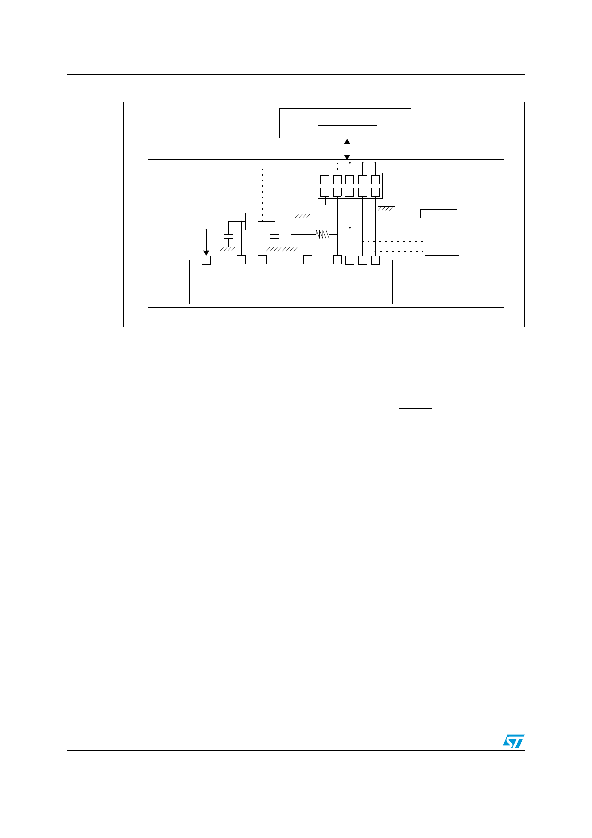
Flash program memory ST72361xx-Auto
ICC CONNECTOR
ICCDATA
ICCCLK
RESET
V
DD
HE10 CONNECTOR TYPE
APPLICATION
POWER SUPPLY
1
246810
97 5 3
PROGRAMMING TOOL
ICC CONNECTOR
APPLICATION BOARD
ICC Cable
(See Note 3)
10k
V
SS
ICCSEL/VPP
ST7
C
L2
C
L1
OSC1
OSC2
OPTIONAL
See Note 1
See Note 2
APPLICATION
RESET SOURCE
APPLICATION
I/O
(See Note 4)
Figure 7. Typical ICC interface
Note: 1 If the ICCCLK or ICCDATA pins are only used as outputs in the application, no signal
isolation is necessary. As soon as the Programming Tool is plugged to the board, even if an
ICC session is not in progress, the ICCCLK and ICCDATA pins are not available for the
application. If they are used as inputs by the application, isolation such as a serial resistor
has to implemented in case another device forces the signal. Refer to the Programming Tool
documentation for recommended resistor values.
2 During the ICC session, the programming tool must control the RESET
pin. This can lead to
conflicts between the programming tool and the application reset circuit if it drives more than
5mA at high level (push pull output or pull-up resistor < 1K). A schottky diode can be used to
isolate the application RESET circuit in this case. When using a classical RC network with
R > 1K or a reset management IC with open drain output and pull-up resistor > 1K, no
additional components are needed. In all cases the user must ensure that no external reset
is generated by the application during the ICC session.
3 The use of Pin 7 of the ICC connector depends on the Programming Tool architecture. This
pin must be connected when using most ST Programming Tools (it is used to monitor the
application power supply). Please refer to the Programming Tool manual.
4 Pin 9 has to be connected to the OSC1 or OSCIN pin of the ST7 when the clock is not
available in the application or if the selected clock option is not programmed in the option
byte. ST7 devices with multi-oscillator capability need to have OSC2 grounded in this case.
3.5 ICP (in-circuit programming)
32/279 Doc ID 12468 Rev 3
To perform ICP the microcontroller must be switched to ICC (In-Circuit Communication)
mode by an external controller or programming tool.
Depending on the ICP code downloaded in RAM, Flash memory programming can be fully
customized (number of bytes to program, program locations, or selection serial
communication interface for downloading).
When using an STMicroelectronics or third-party programming tool that supports ICP and
the specific microcontroller device, the user needs only to implement the ICP hardware

ST72361xx-Auto Flash program memory
interface on the application board (see Figure 7). For more details on the pin locations, refer
to the device pinout description.
3.6 IAP (in-application programming)
This mode uses a Bootloader program previously stored in Sector 0 by the user (in ICP
mode or by plugging the device in a programming tool).
This mode is fully controlled by user software. This allows it to be adapted to the user
application, (user-defined strategy for entering programming mode, choice of
communications protocol used to fetch the data to be stored, etc.). For example, it is
possible to download code from the SPI, SCI or other type of serial interface and program it
in the Flash. IAP mode can be used to program any of the Flash sectors except Sector 0,
which is write/erase protected to allow recovery in case errors occur during the
programming operation.
3.7 Related documentation
For details on Flash programming and ICC protocol, refer to the ST7 Flash programming
reference manual and to the ST7 ICC protocol reference manual
.
3.8 Register description
Flash Control/Status Register (FCSR)
Read/ write
Reset value: 0000 0000 (00h)
7 0
00000000
This register is reserved for use by Programming Tool software. It controls the Flash
programming and erasing operations.
Table 6. Flash control/status register address and reset value
Address (Hex.) Register label 76543210
0024h
FCSR
Reset value 00000000
Doc ID 12468 Rev 3 33/279

Central processing unit ST72361xx-Auto
4 Central processing unit
4.1 Introduction
This CPU has a full 8-bit architecture and contains six internal registers allowing efficient
8-bit data manipulation.
4.2 Main features
● Enable executing 63 basic instructions
● Fast 8-bit by 8-bit multiply
● 17 main addressing modes (with indirect addressing mode)
● Two 8-bit index registers
● 16-bit stack pointer
● Low power HALT and WAIT modes
● Priority maskable hardware interrupts
● Non-maskable software/hardware interrupts
4.3 CPU registers
The six CPU registers shown in Figure 8 are not present in the memory mapping and are
accessed by specific instructions.
4.3.1 Accumulator (A)
The Accumulator is an 8-bit general purpose register used to hold operands and the results
of the arithmetic and logic calculations and to manipulate data.
4.3.2 Index registers (X and Y)
These 8-bit registers are used to create effective addresses or as temporary storage areas
for data manipulation. (The Cross-Assembler generates a precede instruction (PRE) to
indicate that the following instruction refers to the Y register.)
The Y register is not affected by the interrupt automatic procedures.
4.3.3 Program counter (PC)
The program counter is a 16-bit register containing the address of the next instruction to be
executed by the CPU. It is made of two 8-bit registers PCL (Program Counter Low which is
the LSB) and PCH (Program Counter High which is the MSB).
34/279 Doc ID 12468 Rev 3
ST72361xx-Auto Central processing unit
ACCUMULATOR
X INDEX REGISTER
Y INDEX REGISTER
STACK POINTER
CONDITION CODE REGISTER
PROGRAM COUNTER
70
1C1I1HI0NZ
RESET VALUE = RESET VECTOR @ FFFEh-FFFFh
70
70
70
0
7
15 8
PCH
PCL
15
8
70
RESET VALUE = STACK HIGHER ADDRESS
RESET VALUE =
1X1 1 X1XX
RESET VALUE = XXh
RESET VALUE = XXh
RESET VALUE = XXh
X = Undefined Value
Figure 8. CPU registers
4.3.4 Condition code register (CC)
Read/ write
Reset value: 111x1xxx
7 0
11I1HI0NZC
The 8-bit Condition Code register contains the interrupt masks and four flags representative
of the result of the instruction just executed. This register can also be handled by the PUSH
and POP instructions.
These bits can be individually tested and/or controlled by specific instructions.
Arithmetic management bits
Bit 4 = H Half carry.
This bit is set by hardware when a carry occurs between bits 3 and 4 of the ALU during an
ADD or ADC instructions. It is reset by hardware during the same instructions.
0: No half carry has occurred.
1: A half carry has occurred.
This bit is tested using the JRH or JRNH instruction. The H bit is useful in BCD arithmetic
subroutines.
Bit 2 = N Negative.
This bit is set and cleared by hardware. It is representative of the result sign of the last
arithmetic, logical or data manipulation. It’s a copy of the result 7
0: The result of the last operation is positive or null.
1: The result of the last operation is negative (that is, the most significant bit
is a logic 1).
Doc ID 12468 Rev 3 35/279
th
bit.

Central processing unit ST72361xx-Auto
This bit is accessed by the JRMI and JRPL instructions.
Bit 1 = Z Zero.
This bit is set and cleared by hardware. This bit indicates that the result of the last
arithmetic, logical or data manipulation is zero.
0: The result of the last operation is different from zero.
1: The result of the last operation is zero.
This bit is accessed by the JREQ and JRNE test instructions.
Bit 0 = C Carry/borrow.
This bit is set and cleared by hardware and software. It indicates an overflow or an
underflow has occurred during the last arithmetic operation.
0: No overflow or underflow has occurred.
1: An overflow or underflow has occurred.
This bit is driven by the SCF and RCF instructions and tested by the JRC and JRNC
instructions. It is also affected by the “bit test and branch”, shift and rotate instructions.
Interrupt management bits
Bit 5,3 = I1, I0 Interrupt
The combination of the I1 and I0 bits gives the current interrupt software priority.
Table 7. Interrupt software priority selection
Interrupt software priority I1 I0
Level 0 (main) 1 0
Level 1 0 1
Level 2 0 0
Level 3 (= interrupt disable) 1 1
These two bits are set/cleared by hardware when entering in interrupt. The loaded value is
given by the corresponding bits in the interrupt software priority registers (IxSPR). They can
be also set/cleared by software with the RIM, SIM, IRET, HALT, WFI and PUSH/POP
instructions.
See the interrupt management chapter for more details.
36/279 Doc ID 12468 Rev 3

ST72361xx-Auto Central processing unit
4.3.5 Stack pointer (SP)
Read/ write
Reset value: 01 FFh
15 8
00000001
7 0
SP7 SP6 SP5 SP4 SP3 SP2 SP1 SP0
The Stack Pointer is a 16-bit register which is always pointing to the next free location in the
stack. It is then decremented after data has been pushed onto the stack and incremented
before data is popped from the stack (see Figure 9).
Since the stack is 256 bytes deep, the 8 most significant bits are forced by hardware.
Following an MCU Reset, or after a Reset Stack Pointer instruction (RSP), the Stack Pointer
contains its reset value (the SP7 to SP0 bits are set) which is the stack higher address.
The least significant byte of the Stack Pointer (called S) can be directly accessed by a LD
instruction.
Note: When the lower limit is exceeded, the Stack Pointer wraps around to the stack upper limit,
without indicating the stack overflow. The previously stored information is then overwritten
and therefore lost. The stack also wraps in case of an underflow.
The stack is used to save the return address during a subroutine call and the CPU context
during an interrupt. The user may also directly manipulate the stack by means of the PUSH
and POP instructions. In the case of an interrupt, the PCL is stored at the first location
pointed to by the SP. Then the other registers are stored in the next locations as shown in
Figure 9.
● When an interrupt is received, the SP is decremented and the context is pushed on the
stack.
● On return from interrupt, the SP is incremented and the context is popped from the
stack.
A subroutine call occupies two locations and an interrupt five locations in the stack area.
Doc ID 12468 Rev 3 37/279

Central processing unit ST72361xx-Auto
PCH
PCL
SP
PCH
PCL
SP
PCL
PCH
X
A
CC
PCH
PCL
SP
PCL
PCH
X
A
CC
PCH
PCL
SP
PCL
PCH
X
A
CC
PCH
PCL
SP
SP
Y
CALL
Subroutine
Interrupt
Event
PUSH Y POP Y IRET
RET
or RSP
@ 01FFh
@ 0100h
Stack Higher Address = 01FFh
Stack Lower Address =
0100h
Figure 9. Stack manipulation example
38/279 Doc ID 12468 Rev 3
ST72361xx-Auto Supply, reset and clock management
0
1
PLL OPTION BIT
PLL x 2
f
OSC2
/ 2
f
OSC
5 Supply, reset and clock management
5.1 Introduction
The device includes a range of utility features for securing the application in critical
situations (for example, in case of a power brown-out), and reducing the number of external
components. An overview is shown in Figure 11.
For more details, refer to dedicated parametric section.
5.2 Main features
● Optional PLL for multiplying the frequency by 2
● Reset Sequence Manager (RSM)
● Multi-Oscillator Clock Management (MO)
– 4 Crystal/Ceramic resonator oscillators
● System Integrity Management (SI)
– Main supply Low voltage detection (LVD)
– Auxiliary Voltage detector (AVD) with interrupt capability for monitoring the main
supply
5.3 Phase locked loop
If the clock frequency input to the PLL is in the range 2 to 4 MHz, the PLL can be used to
multiply the frequency by two to obtain an f
byte. If the PLL is disabled, then f
OSC2 =fOSC
Caution: The PLL is not recommended for applications where timing accuracy is required.
Section 20.5.2: PLL characteristics
Figure 10. PLL block diagram
of 4 to 8 MHz. The PLL is enabled by option
OSC2
/2.
Doc ID 12468 Rev 3 39/279

Supply, reset and clock management ST72361xx-Auto
LOW VOLTAGE
DETECTOR
(LVD)
AUXILIARY VOLTAGE
DETECTOR
(AVD)
MULTI-
OSCILLATOR
(MO)
OSC1
RESET
V
SS
V
DD
RESET SEQUENCE
MANAGER
(RSM)
OSC2
MAIN CLOCK
AVD Interrupt Request
CONTROLLER
PLL
SYSTEM INTEGRITY MANAGEMENT
WATCHDOG
SICSR
TIMER (WDG)
WITH REALTIME
CLOCK (MCC/RTC)
AVD AVD
LVD
RF
IE
WDG
RF
f
OSC
f
OSC2
(option)
0
0
F
f
CPU
00
8-BIT TIMER
/ 8000
Figure 11. Clock, reset and supply block diagram
5.4 Multi-oscillator (MO)
The main clock of the ST7 can be generated by two different source types coming from the
multi-oscillator block:
● an external source
● a crystal or ceramic resonator oscillator
Each oscillator is optimized for a given frequency range in terms of consumption and is
selectable through the option byte. The associated hardware configuration are shown in
Ta bl e 8 . Refer to the electrical characteristics section for more details.
Caution: The OSC1 and/or OSC2 pins must not be left unconnected. For the purposes of Failure
Mode and Effect Analysis, it should be noted that if the OSC1 and/or OSC2 pins are left
unconnected, the ST7 main oscillator may start and, in this configuration, could generate an
f
clock frequency in excess of the allowed maximum (> 16 MHz), putting the ST7 in an
OSC
unsafe/undefined state. The product behavior must therefore be considered undefined when
the OSC pins are left unconnected.
External clock source
In external clock mode, a clock signal (square, sinus or triangle) with ~50% duty cycle has to
drive the OSC1 pin while the OSC2 pin is tied to ground.
Crystal/ceramic oscillators
This family of oscillators has the advantage of producing a very accurate rate on the main
clock of the ST7. The selection within a list of five oscillators with different frequency ranges
must be done by option byte in order to reduce consumption (refer to Section 22.2.1: Flash
configuration for more details on the frequency ranges). The resonator and the load
capacitors must be placed as close as possible to the oscillator pins in order to minimize
40/279 Doc ID 12468 Rev 3
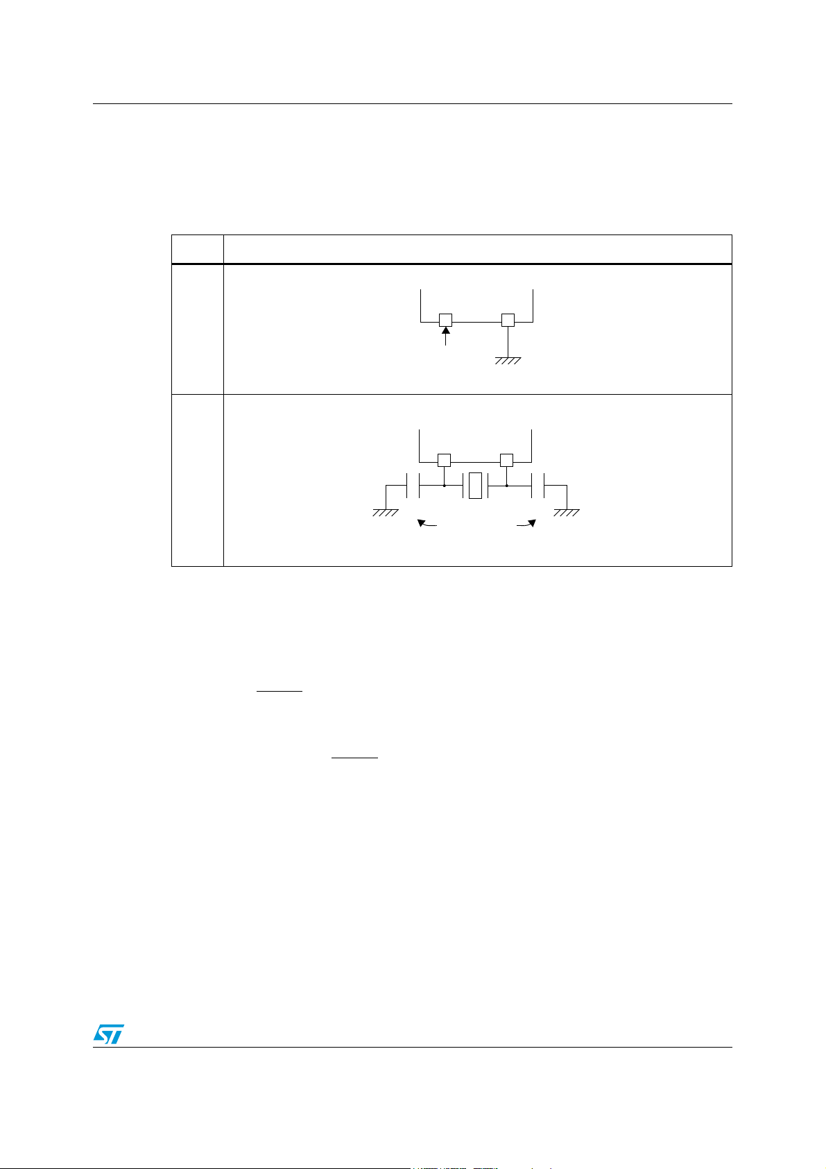
ST72361xx-Auto Supply, reset and clock management
OSC1 OSC2
EXTERNAL
ST7
SOURCE
OSC1 OSC2
LOAD
CAPACITORS
ST7
C
L2
C
L1
output distortion and start-up stabilization time. The loading capacitance values must be
adjusted according to the selected oscillator.
These oscillators are not stopped during the RESET phase to avoid losing time in the
oscillator start-up phase.
Table 8. ST7 clock sources
Hardware configuration
External clockCrystal/Ceramic resonators
5.5 Reset sequence manager (RSM)
5.5.1 Introduction
The reset sequence manager includes three RESET sources as shown in Figure 13:
● External RESET source pulse
● Internal LVD reset (Low Voltage Detection)
● Internal watchdog reset
These sources act on the RESET
The reset service routine vector is fixed at addresses FFFEh-FFFFh in the ST7 memory
map.
The basic RESET sequence consists of three phases as shown in Figure 12:
● Active phase depending on the reset source
● 256 or 4096 CPU clock cycle delay (selected by option byte)
● RESET vector fetch
The 256 or 4096 CPU clock cycle delay allows the oscillator to stabilize and ensures that
recovery has taken place from the Reset state. The shorter or longer clock cycle delay
should be selected by option byte to correspond to the stabilization time of the external
oscillator used in the application.
pin and it is always kept low during the delay phase.
Doc ID 12468 Rev 3 41/279

Supply, reset and clock management ST72361xx-Auto
RESET
Active Phase
INTERNAL RESET
256 or 4096 CLOCK CYCLES
FETCH
VECTOR
RESET
R
ON
V
DD
WATCHDOG RESET
LVD RESET
INTERNAL
RESET
PULSE
GENERATOR
Filter
The reset vector fetch phase duration is two clock cycles.
Figure 12. RESET sequence phases
5.5.2 Asynchronous external RESET pin
The RESET pin is both an input and an open-drain output with integrated RON weak pull-up
resistor. This pull-up has no fixed value but varies in accordance with the input voltage. It
can be pulled low by external circuitry to reset the device. See Chapter 20: Electrical
characteristics for more details.
A reset signal originating from an external source must have a duration of at least t
in order to be recognized (see Figure 14). This detection is asynchronous and therefore the
MCU can enter reset state even in HALT mode.
Figure 13. Reset block diagram
The RESET
pin is an asynchronous signal which plays a major role in EMS performance. In
a noisy environment, it is recommended to follow the guidelines mentioned in the electrical
characteristics section.
5.5.3 External power-on reset
h(RSTL)in
If the LVD is disabled by option byte, to start up the microcontroller correctly, the user must
ensure by means of an external reset circuit that the reset signal is held low until V
the minimum level specified for the selected f
A proper reset signal for a slow rising V
RC network connected to the RESET
supply can generally be provided by an external
DD
pin.
frequency.
OSC
5.5.4 Internal low voltage detector (LVD) reset
Two different reset sequences caused by the internal LVD circuitry can be distinguished:
● Power-on reset
● Voltage drop reset
42/279 Doc ID 12468 Rev 3
is over
DD
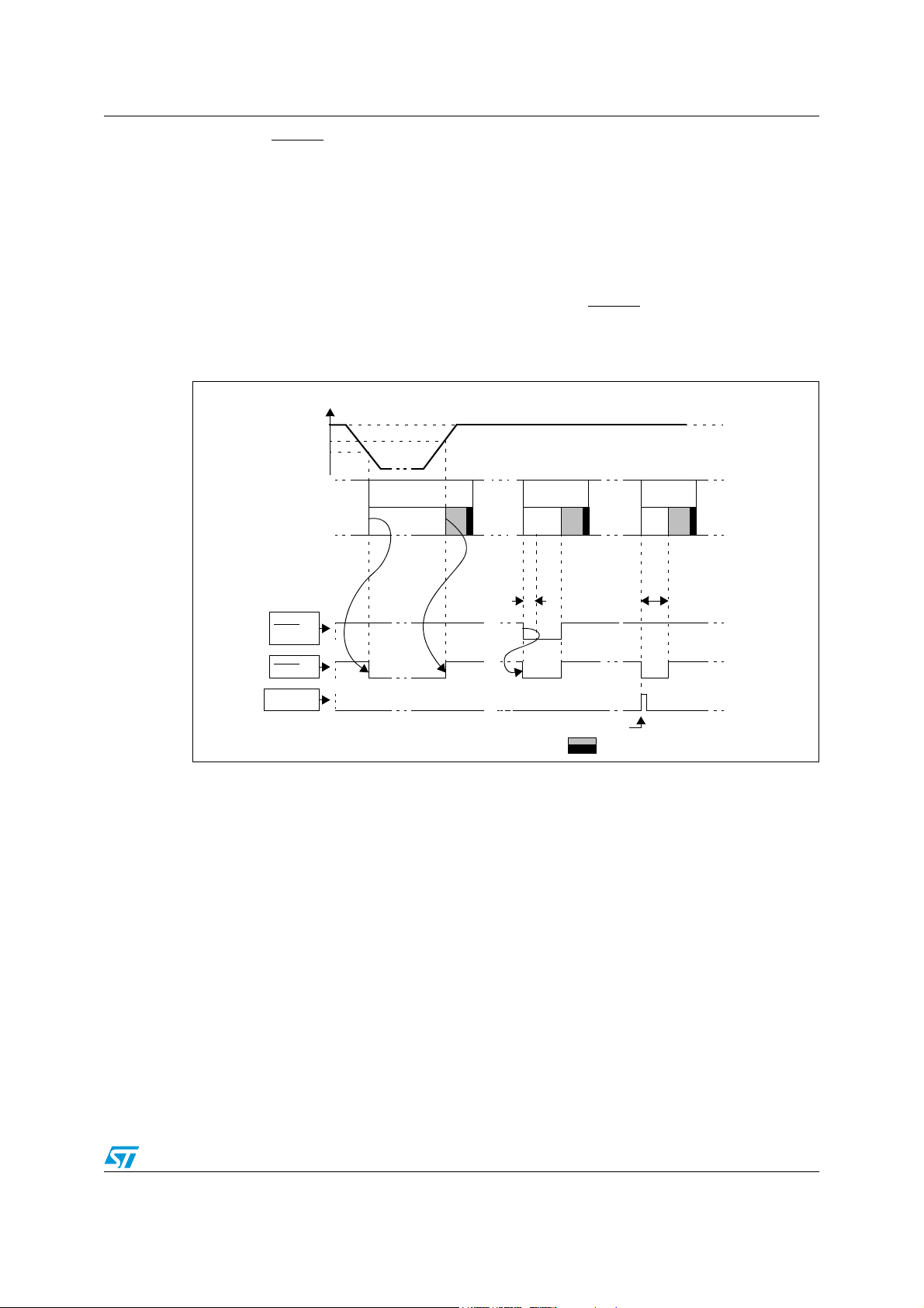
ST72361xx-Auto Supply, reset and clock management
V
DD
RUN
RESET PIN
EXTERNAL
WATCHDOG
ACTIVE PHASE
V
IT+(LVD)
V
IT-(LVD)
t
h(RSTL)in
RUN
WATCHDOG UNDERFLOW
t
w(RSTL)out
RUN RUN
RESET
RESET
SOURCE
EXTERNAL
RESET
LVD
RESET
WATCHDOG
RESET
INTERNAL RESET (256 or 4096 T
CPU
)
VECTOR FETCH
ACTIVE
PHASE
ACTIVE
PHASE
The device RESET pin acts as an output that is pulled low when VDD<V
V
DD<VIT-
The LVD filters spikes on V
(falling edge) as shown in Figure 14.
DD
5.5.5 Internal watchdog reset
The RESET sequence generated by a internal Watchdog counter overflow is shown in
Figure 14.
Starting from the Watchdog counter underflow, the device RESET
is pulled low during at least t
Figure 14. Reset sequences
w(RSTL)out
larger than t
.
to avoid parasitic resets.
g(VDD)
(rising edge) or
IT+
pin acts as an output that
5.6 System integrity management (SI)
The System Integrity Management block contains the Low Voltage Detector (LVD) and
Auxiliary Voltage Detector (AVD) functions. It is managed by the SICSR register.
5.6.1 Low voltage detector (LVD)
The Low Voltage Detector function (LVD) generates a static reset when the VDD supply
voltage is below a V
reference value. This means that it secures the power-up as well
IT-(LVD)
as the power-down keeping the ST7 in reset.
The V
for power-on in order to avoid a parasitic reset when the MCU starts running and sinks
current on the supply (hysteresis).
The LVD reset circuitry generates a reset when V
● V
● V
reference value for a voltage drop is lower than the V
IT-(LVD)
IT+(LVD)
IT-(LVD)
when VDD is rising
when VDD is falling
Doc ID 12468 Rev 3 43/279
is below:
DD
IT+(LVD)
reference value

Supply, reset and clock management ST72361xx-Auto
V
DD
V
IT+
(LVD)
RESET
V
IT-
(LVD)
V
hys
The LVD function is illustrated in Figure 15.
Provided the minimum V
value (guaranteed for the oscillator frequency) is above V
DD
the MCU can only be in two modes:
● under full software control
● in static safe reset
In these conditions, secure operation is always ensured for the application without the need
for external reset hardware.
During a Low Voltage Detector Reset, the RESET
pin is held low, thus permitting the MCU
to reset other devices.
Note: The LVD allows the device to be used without any external RESET circuitry.
The LVD is an optional function which can be selected by option byte.
It is recommended to make sure that the V
supply voltage rises monotonously when the
DD
device is exiting from Reset, to ensure the application functions properly.
Figure 15. Low voltage detector vs reset
IT-(LVD)
,
5.6.2 Auxiliary voltage detector (AVD)
The Voltage Detector function (AVD) is based on an analog comparison between a V
and V
IT+(AVD)
falling voltage is lower than the V
reference value and the VDD main supply. The V
IT+(AVD)
reference value for rising voltage in order to avoid
reference value for
IT-(AVD)
parasitic detection (hysteresis).
The output of the AVD comparator is directly readable by the application software through a
real time status bit (AVDF) in the SICSR register. This bit is read only.
Caution: The AVD function is active only if the LVD is enabled through the option byte.
Monitoring the VDD main supply
If the AVD interrupt is enabled, an interrupt is generated when the voltage crosses the
V
IT+(AVD)
In the case of a drop in voltage, the AVD interrupt acts as an early warning, allowing
software to shut down safely before the LVD resets the microcontroller (see Figure 16).
The interrupt on the rising edge is used to inform the application that the V
is over.
If the voltage rise time t
selected by option byte), no AVD interrupt will be generated when V
44/279 Doc ID 12468 Rev 3
or V
threshold (AVDF bit toggles).
IT-(AVD)
is less than 256 or 4096 CPU cycles (depending on the reset delay
rv
IT+(AVD)
warning state
DD
is reached.
IT-(AVD)

ST72361xx-Auto Supply, reset and clock management
V
DD
V
IT+(AVD)
V
IT-(AVD)
AVDF bit 0 0RESET VALUE
IF AVDIE bit = 1
V
hyst
AVD INTERRUPT
REQUEST
INTERRUPT PROCESS
INTERRUPT PROCESS
V
IT+(LVD)
V
IT-(LVD)
LVD RESET
Early Warning Interrupt
(Power has dropped, MCU not
not yet in reset)
1
1
t
rv
VOLTAGE RISE TIME
If trv is greater than 256 or 4096 cycles then:
● If the AVD interrupt is enabled before the V
IT+(AVD)
threshold is reached, then two AVD
interrupts will be received: The first when the AVDIE bit is set and the second when the
threshold is reached.
● If the AVD interrupt is enabled after the V
IT+(AVD)
threshold is reached, then only one
AVD interrupt occurs.
Figure 16. Using the AVD to monitor V
5.6.3 Low power modes
Table 9. Effect of low power modes on SI
DD
Mode Description
WAIT No effect on SI. AVD interrupts cause the device to exit from Wait mode.
HALT The SICSR register is frozen.
5.6.4 Interrupts
The AVD interrupt event generates an interrupt if the AVDIE bit is set and the interrupt mask
in the CC register is reset (RIM instruction).
Table 10. Interrupt control/wake-up capability
AVD event AVDF AVDIE Yes No
Interrupt event
Event
flag
Doc ID 12468 Rev 3 45/279
Enable
control
bit
Exit
from
wait
Exit
from
halt

Supply, reset and clock management ST72361xx-Auto
5.6.5 Register description
System integrity (SI) control/status register (SICSR)
Read/Write
Reset value: 000x 000x (00h)
7 0
0 AVDIE AVDF LVDRF 0 0 0 WDGRF
Bit 7 = Reserved, must be kept cleared.
Bit 6 = AVDIE Voltage Detector interrupt enable
This bit is set and cleared by software. It enables an interrupt to be generated when the
AVDF flag changes (toggles). The pending interrupt information is automatically cleared
when software enters the AVD interrupt routine.
0: AVD interrupt disabled
1: AVD interrupt enabled
Bit 5 = AVDF Voltage Detector flag
This read-only bit is set and cleared by hardware. If the AVDIE bit is set, an interrupt request
is generated when the AVDF bit changes value. Refer to Figure 16 and to Monitoring the
VDD main supply for additional details.
0: V
over V
1: V
DD
under V
DD
IT+(AVD)
Bit 4 = LVDRF LVD reset flag
This bit indicates that the last Reset was generated by the LVD block. It is set by hardware
(LVD reset) and cleared by software (writing zero). See WDGRF flag description for more
details. When the LVD is disabled by OPTION BYTE, the LVDRF bit value is undefined.
IT-(AVD)
threshold
threshold
Bits 3:1 = Reserved, must be kept cleared.
Bit 0 = WDGRF Watchdog reset flag
This bit indicates that the last Reset was generated by the Watchdog peripheral. It is set by
hardware (watchdog reset) and cleared by software (writing zero) or an LVD Reset (to
ensure a stable cleared state of the WDGRF flag when CPU starts). Combined with the
LVDRF flag information, the flag description is given by the following table.
46/279 Doc ID 12468 Rev 3

ST72361xx-Auto Supply, reset and clock management
Table 11. Reset source flags
RESET sources LVDRF WDGRF
External RESET
Watchdog 1
LV D 1 X
pin
0
0
Application notes
The LVDRF flag is not cleared when another RESET type occurs (external or watchdog), the
LVDRF flag remains set to keep trace of the original failure.
In this case, a watchdog reset can be detected by software while an external reset can not.
Caution: When the LVD is not activated with the associated option byte, the WDGRF flag cannot be
used in the application.
Doc ID 12468 Rev 3 47/279

Interrupts ST72361xx-Auto
6 Interrupts
6.1 Introduction
The ST7 enhanced interrupt management provides the following features:
● Hardware interrupts
● Software interrupt (TRAP)
● Nested or concurrent interrupt management with flexible interrupt priority and level
management:
– Up to 4 software programmable nesting levels
– Up to 16 interrupt vectors fixed by hardware
– 2 non maskable events: RESET, TRAP
– 1 maskable Top Level Event: TLI
This interrupt management is based on:
● Bit 5 and bit 3 of the CPU CC register (I1:0),
● Interrupt software priority registers (ISPRx),
● Fixed interrupt vector addresses located at the high addresses of the memory map
(FFE0h to FFFFh) sorted by hardware priority order.
This enhanced interrupt controller guarantees full upward compatibility with the standard
(not nested) ST7 interrupt controller.
6.2 Masking and processing flow
The interrupt masking is managed by the I1 and I0 bits of the CC register and the ISPRx
registers which give the interrupt software priority level of each interrupt vector (see
Ta bl e 1 2 ). The processing flow is shown in Figure 17.
When an interrupt request has to be serviced:
● Normal processing is suspended at the end of the current instruction execution.
● The PC, X, A and CC registers are saved onto the stack.
● I1 and I0 bits of CC register are set according to the corresponding values in the ISPRx
registers of the serviced interrupt vector.
● The PC is then loaded with the interrupt vector of the interrupt to service and the first
instruction of the interrupt service routine is fetched (refer to “Interrupt Mapping” table
for vector addresses).
The interrupt service routine should end with the IRET instruction which causes the
contents of the saved registers to be recovered from the stack.
Note: As a consequence of the IRET instruction, the I1 and I0 bits will be restored from the stack
and the program in the previous level will resume.
48/279 Doc ID 12468 Rev 3

ST72361xx-Auto Interrupts
“IRET”
RESTORE PC, X, A, CC
STACK PC, X, A, CC
LOAD I1:0 FROM INTERRUPT SW REG.
FETCH NEXT
RESET
TLI
PENDING
INSTRUCTION
I1:0
FROM STACK
LOAD PC FROM INTERRUPT VECTOR
Y
N
Y
N
Y
N
Interrupt has the same or a
lower software priority
THE INTERRUPT
STAYS PENDING
than current one
Interrupt has a higher
software priority
than current one
EXECUTE
INSTRUCTION
INTERRUPT
PENDING
SOFTWARE
Different
INTERRUPTS
Same
HIGHEST HARDWARE
PRIORITY SERVICED
PRIORITY
HIGHEST SOFTWARE
PRIORITY SERVICED
Table 12. Interrupt software priority levels
Interrupt software priority Level I1 I0
Level 0 (main)
Level 1
Low
10
0
Level 2 0
High
Level 3 (= interrupt disable) 1 1
Figure 17. Interrupt processing flowchart
1
Servicing pending interrupts
As several interrupts can be pending at the same time, the interrupt to be taken into account
is determined by the following two-step process:
● the highest software priority interrupt is serviced,
● if several interrupts have the same software priority then the interrupt with the highest
hardware priority is serviced first.
Figure 18 describes this decision process.
Figure 18. Priority decision process
Doc ID 12468 Rev 3 49/279

Interrupts ST72361xx-Auto
When an interrupt request is not serviced immediately, it is latched and then processed
when its software priority combined with the hardware priority becomes the highest one.
Note: 1 The hardware priority is exclusive while the software one is not. This allows the previous
process to succeed with only one interrupt.
2 RESET, TRAP and TLI can be considered as having the highest software priority in the
decision process.
Different interrupt vector sources
Two interrupt source types are managed by the ST7 interrupt controller: the non-maskable
type (RESET, TRAP) and the maskable type (external or from internal peripherals).
Non-maskable sources
These sources are processed regardless of the state of the I1 and I0 bits of the CC register
(see Figure 17). After stacking the PC, X, A and CC registers (except for RESET), the
corresponding vector is loaded in the PC register and the I1 and I0 bits of the CC are set to
disable interrupts (level 3). These sources allow the processor to exit HALT mode.
● TRAP (Non Maskable Software Interrupt)
Caution: This software interrupt is serviced when the TRAP instruction is executed. It will be serviced
according to the flowchart in Figure 17 as a TLI.
TRAP can be interrupted by a TLI.
● RESET
The RESET source has the highest priority in the ST7. This means that the first current
routine has the highest software priority (level 3) and the highest hardware priority.
See the RESET chapter for more details.
Maskable sources
Maskable interrupt vector sources can be serviced if the corresponding interrupt is enabled
and if its own interrupt software priority (in ISPRx registers) is higher than the one currently
being serviced (I1 and I0 in CC register). If any of these two conditions is false, the interrupt
is latched and thus remains pending.
● TLI (Top Level Hardware Interrupt)
Caution: This hardware interrupt occurs when a specific edge is detected on the dedicated TLI pin.
A TRAP instruction must not be used in a TLI service routine.
● External Interrupts
External interrupts allow the processor to exit from HALT low power mode.
External interrupt sensitivity is software selectable through the External Interrupt Control
register (EICR).
External interrupt triggered on edge will be latched and the interrupt request automatically
cleared upon entering the interrupt service routine.
If several input pins of a group connected to the same interrupt line are selected
simultaneously, these will be logically ORed.
● Peripheral Interrupts
Usually the peripheral interrupts cause the MCU to exit from HALT mode except those
mentioned in the “Interrupt Mapping” table.
A peripheral interrupt occurs when a specific flag is set in the peripheral status registers and
50/279 Doc ID 12468 Rev 3

ST72361xx-Auto Interrupts
MAIN
IT4
IT2
IT1
TLI
IT1
MAIN
IT0
I1
HARDWARE PRIORITY
SOFTWARE
3
3
3
3
3
3/0
3
11
11
11
11
11
11 / 10
11
RIM
IT2
IT1
IT4
TLI
IT3
IT0
IT3
I0
10
PRIORITY
LEVEL
USED STACK = 10 BYTES
if the corresponding enable bit is set in the peripheral control register.
The general sequence for clearing an interrupt is based on an access to the status register
followed by a read or write to an associated register.
Note: The clearing sequence resets the internal latch. A pending interrupt (that is, waiting for
being serviced) will therefore be lost if the clear sequence is executed.
6.3 Interrupts and low power modes
All interrupts allow the processor to exit the WAIT low power mode. On the contrary, only
external and other specified interrupts allow the processor to exit from the HALT modes (see
column “Exit from HALT” in “Interrupt Mapping” table). When several pending interrupts are
present while exiting HALT mode, the first one serviced can only be an interrupt with exit
from HALT mode capability and it is selected through the same decision process shown in
Figure 18.
Note: If an interrupt, that is not able to Exit from HALT mode, is pending with the highest priority
when exiting HALT mode, this interrupt is serviced after the first one serviced.
6.4 Concurrent & nested management
The following Figure 19 and Figure 20 show two different interrupt management modes. The
first is called concurrent mode and does not allow an interrupt to be interrupted, unlike the
nested mode in Figure 20. The interrupt hardware priority is given in this order from the
lowest to the highest: MAIN, IT4, IT3, IT2, IT1, IT0, TLI. The software priority is given for
each interrupt.
Warning: A stack overflow may occur without notifying the software of
the failure.
Figure 19. Concurrent interrupt management
Doc ID 12468 Rev 3 51/279
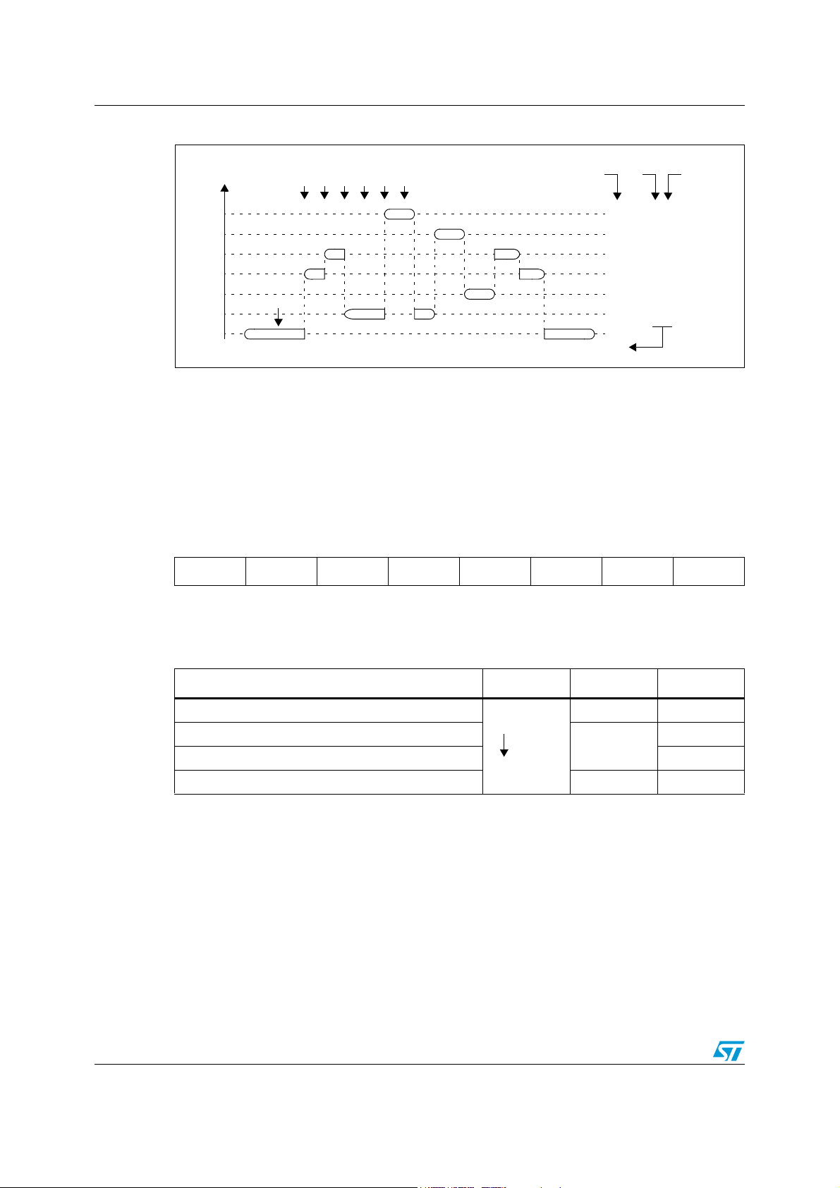
Interrupts ST72361xx-Auto
MAIN
IT2
TLI
MAIN
IT0
IT2
IT1
IT4
TLI
IT3
IT0
HARDWARE PRIORITY
3
2
1
3
3
3/0
3
11
00
01
11
11
11
RIM
IT1
IT4
IT4
IT1
IT2
IT3
I1 I0
11 / 10
10
SOFTWARE
PRIORITY
LEVEL
USED STACK = 20 BYTES
Figure 20. Nested interrupt management
6.5 Interrupt register description
6.5.1 CPU CC register interrupt bits
Read/Write
Reset value: 111x 1010 (xAh)
7 0
11I1HI0NZC
Bit 5, 3 = I1, I0 Software Interrupt Priority
These two bits indicate the current interrupt software priority.
Table 13. Interrupt software priority levels
Interrupt software priority Level I1 I0
Level 0 (main)
Level 1
Low
10
1
0
Level 2 0
Level 3 (= interrupt disable
1. TLI, TRAP and RESET events can interrupt a level 3 program.
(1)
)
High
11
These two bits are set/cleared by hardware when entering in interrupt. The loaded value is
given by the corresponding bits in the interrupt software priority registers (ISPRx).
They can be also set/cleared by software with the RIM, SIM, HALT, WFI, IRET and
PUSH/POP instructions (see Table 15: Dedicated interrupt instruction set on page 55).
52/279 Doc ID 12468 Rev 3

ST72361xx-Auto Interrupts
6.5.2 Interrupt software priority registers (ISPRX)
Read/ write (bit 7:4 of ISPR3 are read only)
Reset value: 1111 1111 (FFh)
70
ISPR0 I1_3 I0_3 I1_2 I0_2 I1_1 I0_1 I1_0 I0_0
ISPR1 I1_7 I0_7 I1_6 I0_6 I1_5 I0_5 I1_4 I0_4
ISPR2 I1_11 I0_11 I1_10 I0_10 I1_9 I0_9 I1_8 I0_8
ISPR3 1 1 1 1 I1_13 I0_13 I1_12 I0_12
These four registers contain the interrupt software priority of each interrupt vector.
● Each interrupt vector (except RESET and TRAP) has corresponding bits in these
registers where its own software priority is stored. This correspondence is shown in the
following table.
Table 14. Interrupt priority bits
Vector address ISPRx bits
FFFBh-FFFAh I1_0 and I0_0 bits
FFF9h-FFF8h I1_1 and I0_1 bits
... ...
(1)
FFE1h-FFE0h I1_13 and I0_13 bits
1. Bits in the ISPRx registers which correspond to the TLI can be read and written but they are not significant
in the interrupt process management.
● Each I1_x and I0_x bit value in the ISPRx registers has the same meaning as the I1
and I0 bits in the CC register.
● Level 0 cannot be written (I1_x = 1, I0_x = 0). In this case, the previously stored value
is kept (Example: previous = CFh, write = 64h, result = 44h)
The RESET, TRAP and TLI vectors have no software priorities. When one is serviced, the I1
and I0 bits of the CC register are both set.
Caution: If the I1_x and I0_x bits are modified while the interrupt x is executed the following behavior
has to be considered: If the interrupt x is still pending (new interrupt or flag not cleared) and
the new software priority is higher than the previous one, the interrupt x is re-entered.
Otherwise, the software priority stays unchanged up to the next interrupt request (after the
IRET of the interrupt x).
Table 15. Dedicated interrupt instruction set
Instruction New description Function/example I1 H I0 N Z C
HALT Entering Halt mode 1 0
IRET Interrupt routine return Pop CC, A, X, PC I1 H I0 N Z C
JRM Jump if I1:0 = 11 (level 3) I1:0 = 11 ?
JRNM Jump if I1:0 <> 11 I1:0 <> 11?
Doc ID 12468 Rev 3 53/279

Interrupts ST72361xx-Auto
Table 15. Dedicated interrupt instruction set (continued)
Instruction New description Function/example I1 H I0 N Z C
POP CC Pop CC from the Stack Mem => CC I1 H I0 N Z C
RIM Enable interrupt (level 0 set) Load 10 in I1:0 of CC 1 0
SIM Disable interrupt (level 3 set) Load 11 in I1:0 of CC 1 1
TRAP Software trap Software NMI 1 1
WFI Wait for interrupt 1 0
Note: During the execution of an interrupt routine, the HALT, POPCC, RIM, SIM and WFI
instructions change the current software priority up to the next IRET instruction or one of the
previously mentioned instruction
54/279 Doc ID 12468 Rev 3
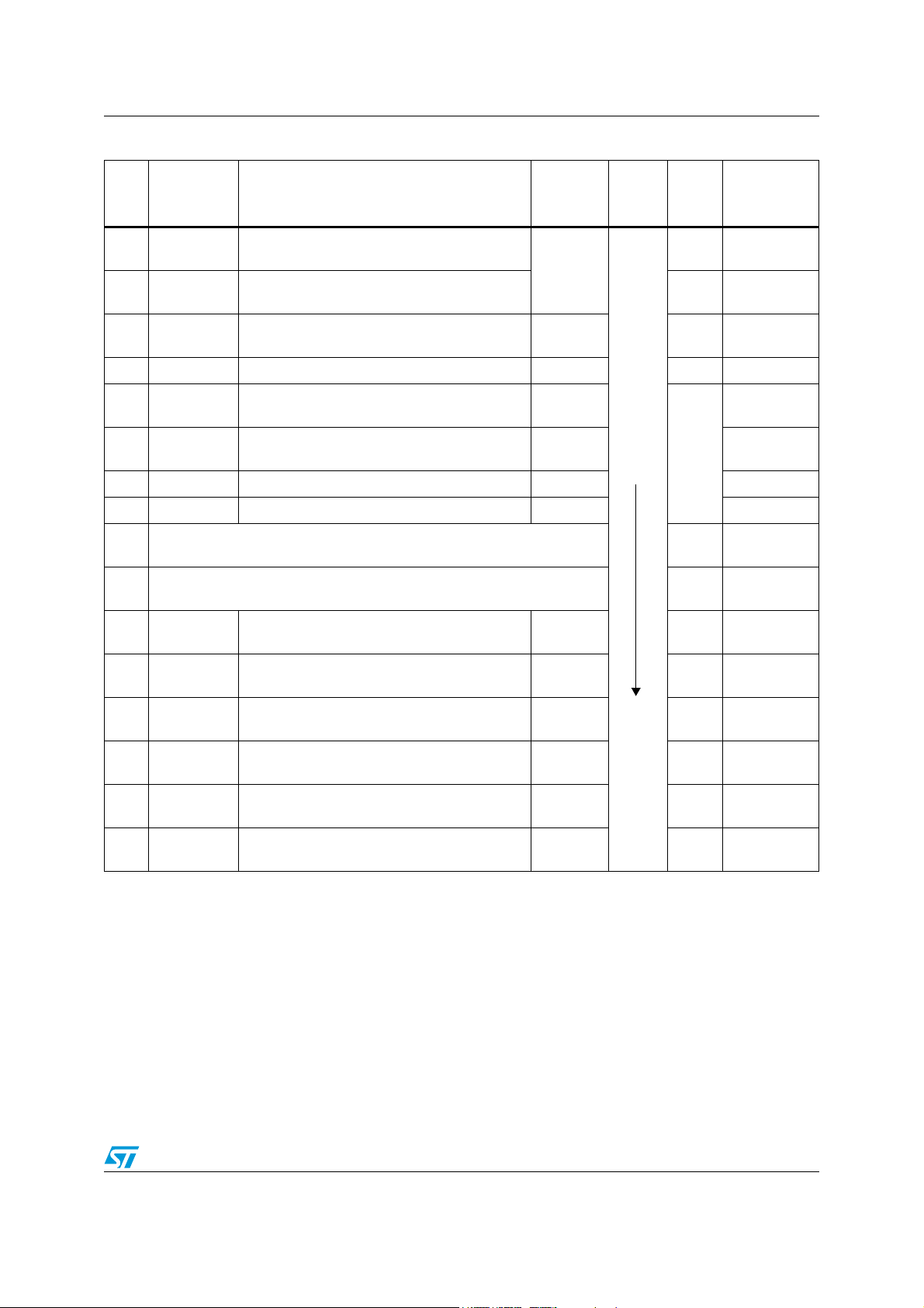
ST72361xx-Auto Interrupts
Table 16. Interrupt mapping
N°
Source
block
RESET Reset
Description
Register
label
Priority
order
Exit
from
Halt
yes
(1)
Address
vector
FFFEh-
FFFFh
N/A
TRAP Software interrupt no
0 TLI External top level interrupt EICR yes
FFFCh-
FFFDh
FFFAh-
FFFBh
1 MCC/RTC Main clock controller time base interrupt MCCSR yes FFF8h-FFF9h
2 ei0/AWUFH External interrupt ei0/ Auto wake-up from Halt
3ei1/AVD
External interrupt ei1/Auxiliary Voltage
Detector
4 ei2 External interrupt ei2 EICR FFF2h-FFF3h
EICR/AW
UCSR
EICR/
SICSR
Highest
Priority
yes
FFF6h-FFF7h
FFF4h-FFF5h
(2)
5 ei3 External interrupt ei3 EICR FFF0h-FFF1h
6 not used
7 not used
8 SPI SPI peripheral interrupts SPICSR yes
FFEEh-
FFEFh
FFECh-
FFEDh
FFEAh-
FFEBh
9 TIMER8 8-bit TIMER peripheral interrupts T8_TCR1 no
10 TIMER16 16-bit TIMER peripheral interrupts TCR1 no
Lowest
Priority
11 LINSCI2 LINSCI2 Peripheral interrupts SCI2CR1 no
12 LINSCI1
LINSCI1 Peripheral interrupts (LIN
Master/Slave)
SCI1CR1 no
13 PWM ART 8-bit PWM ART interrupts PWMCR yes
1. Valid for HALT and ACTIVE HALT modes except for the MCC/RTC interrupt source which exits from ACTIVE HALT mode
only.
2. Except AVD interrupt.
FFE8h-
FFE9h
FFE6h-
FFE7h
FFE4h-
FFE5h
FFE2h-
FFE3h
FFE0h-
FFE1h
Doc ID 12468 Rev 3 55/279

Interrupts ST72361xx-Auto
6.6 External interrupts
6.6.1 I/O port interrupt sensitivity
The external interrupt sensitivity is controlled by the ISxx bits in the EICR register
(Figure 21). This control allows up to four fully independent external interrupt source
sensitivities.
Each external interrupt source can be generated on four (or five) different events on the pin:
● Falling edge
● Rising edge
● Falling and rising edge
● Falling edge and low level
To guarantee correct functionality, the sensitivity bits in the EICR register can be modified
only when the I1 and I0 bits of the CC register are both set to 1 (level 3). This means that
interrupts must be disabled before changing sensitivity.
The pending interrupts are cleared by writing a different value in the ISx[1:0] of the EICR.
56/279 Doc ID 12468 Rev 3

ST72361xx-Auto Interrupts
IS10 IS11
EICR
SENSITIVITY
CONTROL
PBOR.0
PBDDR.0
PB0
ei1 INTERRUPT SOURCE
PORT B [5:0] INTERRUPTS
PB0
PB1
PB2
PB3
IS20 IS21
EICR
SENSITIVITY
CONTROL
PCOR.7
PCDDR.7
PC1
ei2 INTERRUPT SOURCE
PORT C [2:1] INTERRUPTS
PC1
PC2
IS00 IS01
EICR
SENSITIVITY
CONTROL
PAOR.0
PADDR.0
PA0
ei0 INTERRUPT SOURCE
PORT A [7:0] INTERRUPTS
PA0
PA1
PA2
PA3
PA4
PA5
PA6
PA7
/ AWUPR
AWUFH
Oscillator
To Timer Input Capture 1
PB4
PB5
IS30 IS31
EICR
SENSITIVITY
CONTROL
PDOR.0
PDDDR.0
PD0
ei3 INTERRUPT SOURCE
PORT D [7:6, 4, 1:0] INTERRUPTS
PD0
PD1
PD4
PD6
PD7
Figure 21. External interrupt control bits
Doc ID 12468 Rev 3 57/279

Interrupts ST72361xx-Auto
6.6.2 Register description
External interrupt control register 0 (EICR0)
Read/Write
Reset value: 0000 0000 (00h)
7 0
IS31 IS30 IS21 IS20 IS11 IS10 IS01 IS00
Bits 7:6 = IS3[1:0] ei3 sensitivity
The interrupt sensitivity, defined using the IS3[1:0] bits, is applied to the ei3 external
interrupts:
Table 17. Interrupt sensitivity - ei3
IS31 IS30 External interrupt sensitivity
0
0 Falling edge and low level
1 Rising edge only
0 Falling edge only
1
1 Rising and falling edge
These 2 bits can be written only when I1 and I0 of the CC register are both set to 1 (level 3).
Bits 5:4 = IS2[1:0] ei2 sensitivity
The interrupt sensitivity, defined using the IS2[1:0] bits, is applied to the ei2 external
interrupts:
Table 18. Interrupt sensitivity - ei2
IS21 IS20 External interrupt sensitivity
0 Falling edge and low level
0
1 Rising edge only
0 Falling edge only
1
1 Rising and falling edge
These 2 bits can be written only when I1 and I0 of the CC register are both set to 1 (level 3).
Bits 3:2 = IS1[1:0] ei1 sensitivity
The interrupt sensitivity, defined using the IS1[1:0] bits, is applied to the ei1 external
interrupts:
Table 19. Interrupt sensitivity - ei1
IS11 IS10 External interrupt sensitivity
0 Falling edge and low level
0
1 Rising edge only
58/279 Doc ID 12468 Rev 3

ST72361xx-Auto Interrupts
Table 19. Interrupt sensitivity - ei1
IS11 IS10 External interrupt sensitivity
1
0 Falling edge only
1 Rising and falling edge
These 2 bits can be written only when I1 and I0 of the CC register are both set to 1 (level 3).
Bits 1:0 = IS0[1:0] ei0 sensitivity
The interrupt sensitivity, defined using the IS0[1:0] bits, is applied to the ei0 external
interrupts:
Table 20. Interrupt sensitivity - ei0
IS01 IS00 External interrupt sensitivity
0
1
0 Falling edge and low level
1 Rising edge only
0 Falling edge only
1 Rising and falling edge
These 2 bits can be written only when I1 and I0 of the CC register are both set to 1 (level 3).
External Interrupt Control Register 1 (EICR1)
Read/Write
Reset value: 0000 0000 (00h)
7 0
000000TLISTLIE
BIts 7:2 = Reserved
Bit 1 = TLIS Top Level Interrupt sensitivity
This bit configures the TLI edge sensitivity. It can be set and cleared by software only when
TLIE bit is cleared.
0: Falling edge
1: Rising edge
Bit 0 = TLIE Top Level Interrupt enable
This bit allows to enable or disable the TLI capability on the dedicated pin. It is set and
cleared by software.
0: TLI disabled
1: TLI enabled
Note: A parasitic interrupt can be generated when clearing the TLIE bit.
In some packages, the TLI pin is not available. In this case, the TLIE bit must be kept low to
avoid parasitic TLI interrupts.
Doc ID 12468 Rev 3 59/279

Interrupts ST72361xx-Auto
Table 21. Nested interrupts register map and reset values
Address
(Hex.)
Register
label
76543210
ei1 ei0 CLKM TLI
0025h
0026h
ISPR0
Reset value
ISPR1
Reset value
I1_3
1
I1_7
1
I0_3
1
I0_7
1
I1_2
1
I1_6
1
I0_2
1
I0_6
1
LINSCI 2 TIMER 16 TIMER 8 SPI
0027h
0028h
ISPR2
Reset value
ISPR3
I1_11
1
I0_11
1
I1_10
1
I0_10
1
Reset value1111
0029h
002Ah
EICR0
Reset value
EICR1
Reset value000000
IS31
0
IS30
0
IS21
0
IS20
0
I1_1
1
I0_1
111
ei3 ei2
I1_5
1
I1_9
1
I0_5
1
I0_9
1
ART LINSCI 1
I1_13
1
IS11
0
I0_13
1
IS10
0
I1_4
1
I1_8
1
I1_12
1
IS01
0
TLIS
0
I0_4
1
I0_8
1
I0_12
1
IS00
0
TLIE
0
60/279 Doc ID 12468 Rev 3

ST72361xx-Auto Power saving modes
POWER CONSUMPTION
WAIT
SLOW
RUN
ACTIVE HALT
High
Low
SLOW WAIT
AUTO WAKE-UP FROM HALT
HALT
7 Power saving modes
7.1 Introduction
To give a large measure of flexibility to the application in terms of power consumption, five
main power saving modes are implemented in the ST7 (see Figure 22):
● Slow
● Wait (and Slow-Wait)
● Active Halt
● Auto Wake-up From Halt (AWUFH)
● Halt
After a RESET the normal operating mode is selected by default (RUN mode). This mode
drives the device (CPU and embedded peripherals) by means of a master clock which is
based on the main oscillator frequency divided or multiplied by 2 (f
From RUN mode, the different power saving modes may be selected by setting the relevant
register bits or by calling the specific ST7 software instruction whose action depends on the
oscillator status.
Figure 22. Power saving mode transitions
OSC2
).
7.2 Slow mode
This mode has two targets:
● To reduce power consumption by decreasing the internal clock in the device,
● To adapt the internal clock frequency (f
SLOW mode is controlled by three bits in the MCCSR register: the SMS bit which enables or
disables Slow mode and two CPx bits which select the internal slow frequency (f
Doc ID 12468 Rev 3 61/279
) to the available supply voltage.
CPU
CPU
).

Power saving modes ST72361xx-Auto
00 01
SMS
CP1:0
f
CPU
NEW SLOW
NORMAL RUN MODE
MCCSR
FREQUENCY
REQUEST
REQUEST
f
OSC2
f
OSC2
/2 f
OSC2
/4 f
OSC2
In this mode, the master clock frequency (f
and peripherals are clocked at this lower frequency (f
) can be divided by 2, 4, 8 or 16. The CPU
OSC2
CPU
).
Note: SLOW-WAIT mode is activated by entering WAIT mode while the device is in SLOW mode.
Figure 23. SLOW mode clock transitions
7.3 Wait mode
WAIT mode places the MCU in a low power consumption mode by stopping the CPU.
This power saving mode is selected by calling the ‘WFI’ instruction.
All peripherals remain active. During WAIT mode, the I[1:0] bits of the CC register are forced
to ‘10’, to enable all interrupts. All other registers and memory remain unchanged. The MCU
remains in WAIT mode until an interrupt or RESET occurs, whereupon the Program Counter
branches to the starting address of the interrupt or Reset service routine.
The MCU will remain in WAIT mode until a Reset or an Interrupt occurs, causing it to wake
up.
Refer to Figure 24
62/279 Doc ID 12468 Rev 3

ST72361xx-Auto Power saving modes
WFI INSTRUCTION
RESET
INTERRUPT
Y
N
N
Y
CPU
OSCILLATOR
PERIPHERALS
I[1:0] BITS
ON
ON
10
OFF
FETCH RESET VECTOR
OR SERVICE INTERRUPT
CPU
OSCILLATOR
PERIPHERALS
I[1:0] BITS
ON
OFF
10
ON
CPU
OSCILLATOR
PERIPHERALS
I[1:0] BITS
ON
ON
XX
1)
ON
256 OR 4096 CPU CLOCK
CYCLE DELAY
Figure 24. WAIT mode flow-chart
Note: Before servicing an interrupt, the CC register is pushed on the stack. The I[1:0] bits of the
CC register are set to the current software priority level of the interrupt routine and
recovered when the CC register is popped.
7.4 Halt mode
The HALT mode is the lowest power consumption mode of the MCU. It is entered by
executing the ‘HALT’ instruction when the OIE bit of the Main Clock Controller Status
register (MCCSR) is cleared (see Section 10: Main clock controller with real time clock
MCC/RTC for more details on the MCCSR register) and when the AWUEN bit in the
AWUCSR register is cleared.
The MCU can exit HALT mode on reception of either a specific interrupt (see Ta bl e 1 6 ) or a
RESET. When exiting HALT mode by means of a RESET or an interrupt, the oscillator is
immediately turned on and the 256 or 4096 CPU cycle delay is used to stabilize the
oscillator. After the start up delay, the CPU resumes operation by servicing the interrupt or
by fetching the reset vector which woke it up (see Figure 26).
When entering HALT mode, the I[1:0] bits in the CC register are forced to ‘10b’ to enable
interrupts. Therefore, if an interrupt is pending, the MCU wakes up immediately.
In HALT mode, the main oscillator is turned off causing all internal processing to be stopped,
including the operation of the on-chip peripherals. All peripherals are not clocked except the
ones which get their clock supply from another clock generator (such as an external or
auxiliary oscillator).
The compatibility of Watchdog operation with HALT mode is configured by the “WDGHALT”
option bit of the option byte. The HALT instruction when executed while the Watchdog
Doc ID 12468 Rev 3 63/279
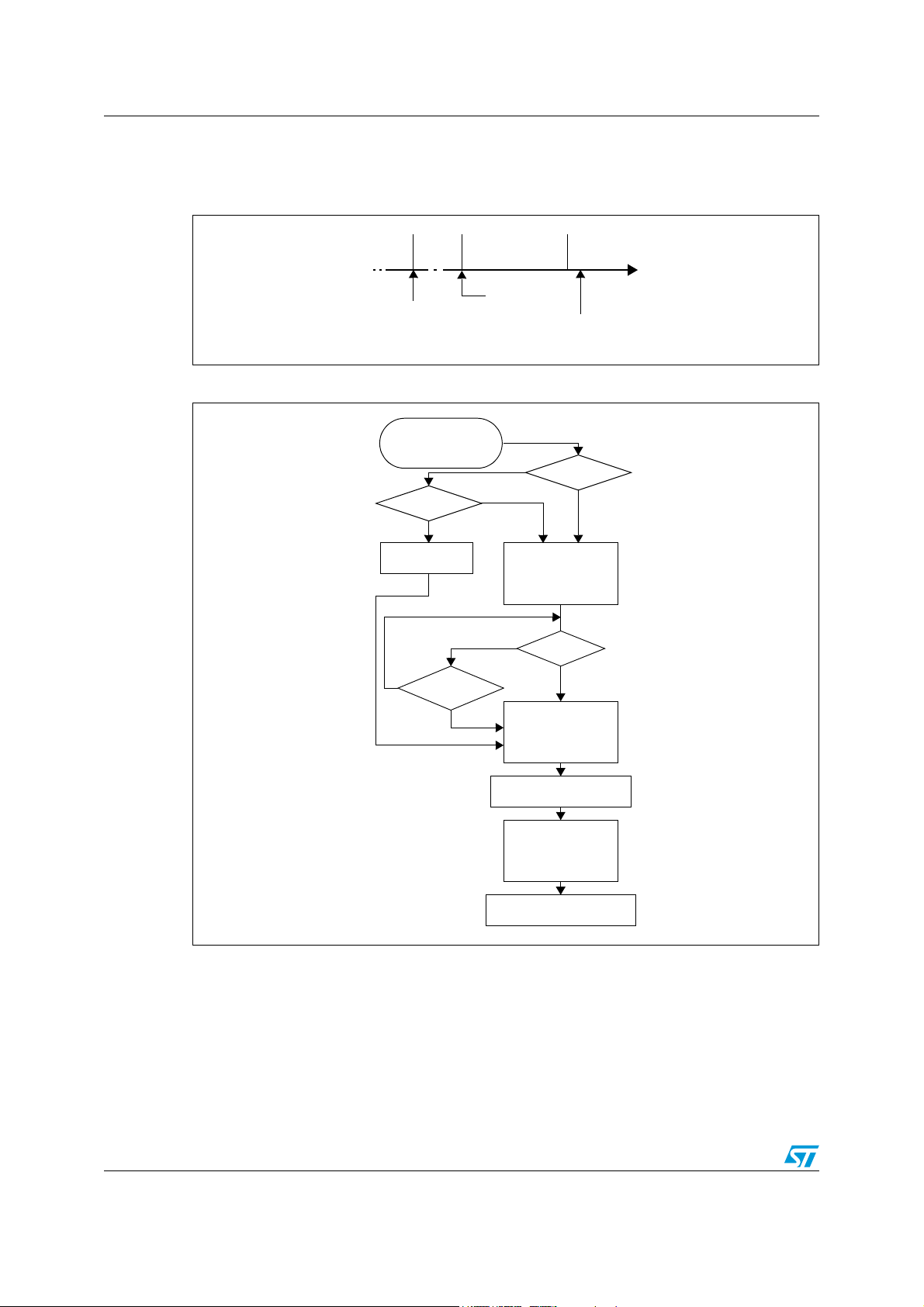
Power saving modes ST72361xx-Auto
HALTRUN RUN
256 OR 4096 CPU
CYCLE DELAY
RESET
OR
INTERRUPT
HALT
INSTRUCTION
FETCH
VECTOR
[MCCSR.OIE=0]
RESET
INTERRUPT
3)
Y
N
N
Y
CPU
OSCILLATOR
PERIPHERALS
2)
I[1:0] BITS
OFF
OFF
10
OFF
FETCH RESET VECTOR
OR SERVICE INTERRUPT
CPU
OSCILLATOR
PERIPHERALS
I[1:0] BITS
ON
OFF
XX
4)
ON
CPU
OSCILLATOR
PERIPHERALS
I[1:0] BITS
ON
ON
XX
4)
ON
256 OR 4096 CPU CLOCK
DELAY
WATCHDOG
ENABLE
DISABLE
WDGHALT
1)
0
WATCHDOG
RESET
1
CYCLE
HALT INSTRUCTION
(MCCSR.OIE=0)
(AWUCSR.AWUEN=0)
system is enabled, can generate a Watchdog RESET (see Section 22.1: Introduction for
more details).
Figure 25. HALT timing overview
Figure 26. HALT mode flow-chart
Note: 1 WDGHALT is an option bit. See option byte section for more details.
2 Peripheral clocked with an external clock source can still be active.
3 Only some specific interrupts can exit the MCU from HALT mode (such as external
interrupt). Refer to Ta b le 1 6 for more details.
4 Before servicing an interrupt, the CC register is pushed on the stack. The I[1:0] bits of the
CC register are set to the current software priority level of the interrupt routine and
recovered when the CC register is popped.
64/279 Doc ID 12468 Rev 3

ST72361xx-Auto Power saving modes
Halt mode recommendations
● Make sure that an external event is available to wake up the microcontroller from Halt
mode.
● When using an external interrupt to wake up the microcontroller, reinitialize the
corresponding I/O as “Input Pull-up with Interrupt” before executing the HALT
instruction. The main reason for this is that the I/O may be wrongly configured due to
external interference or by an unforeseen logical condition.
● For the same reason, reinitialize the level sensitiveness of each external interrupt as a
precautionary measure.
● The opcode for the HALT instruction is 0x8E. To avoid an unexpected HALT instruction
due to a program counter failure, it is advised to clear all occurrences of the data value
0x8E from memory. For example, avoid defining a constant in ROM with the value
0x8E.
● As the HALT instruction clears the interrupt mask in the CC register to allow interrupts,
the user may choose to clear all pending interrupt bits before executing the HALT
instruction. This avoids entering other peripheral interrupt routines after executing the
external interrupt routine corresponding to the wake-up event (reset or external
interrupt).
7.5 Active halt mode
ACTIVE HALT mode is the lowest power consumption mode of the MCU with a real time
clock available. It is entered by executing the ‘HALT’ instruction when MCC/RTC interrupt
enable flag (OIE bit in MCCSR register) is set and when the AWUEN bit in the AWUCSR
register is cleared (Section 7.6.1: Register description)
Table 22. MCC/RTC low power mode selection
MCCSR
OIE bit
0 HALT mode
1 ACTIVE HALT mode
The MCU can exit ACTIVE HALT mode on reception of the RTC interrupt and some specific
interrupts (see Ta b le 1 6 ) or a RESET. When exiting ACTIVE HALT mode by means of a
RESET a 4096 or 256 CPU cycle delay occurs (depending on the option byte). After the
start up delay, the CPU resumes operation by servicing the interrupt or by fetching the reset
vector which woke it up (see Figure 28).
When entering ACTIVE HALT mode, the I[1:0] bits in the CC register are are forced to ‘10b’
to enable interrupts. Therefore, if an interrupt is pending, the MCU wakes up immediately.
In ACTIVE HALT mode, only the main oscillator and its associated counter (MCC/RTC) are
running to keep a wake-up time base. All other peripherals are not clocked except those
which get their clock supply from another clock generator (such as external or auxiliary
oscillator).
Power saving mode entered when HALT instruction is executed
The safeguard against staying locked in ACTIVE HALT mode is provided by the oscillator
interrupt.
Doc ID 12468 Rev 3 65/279
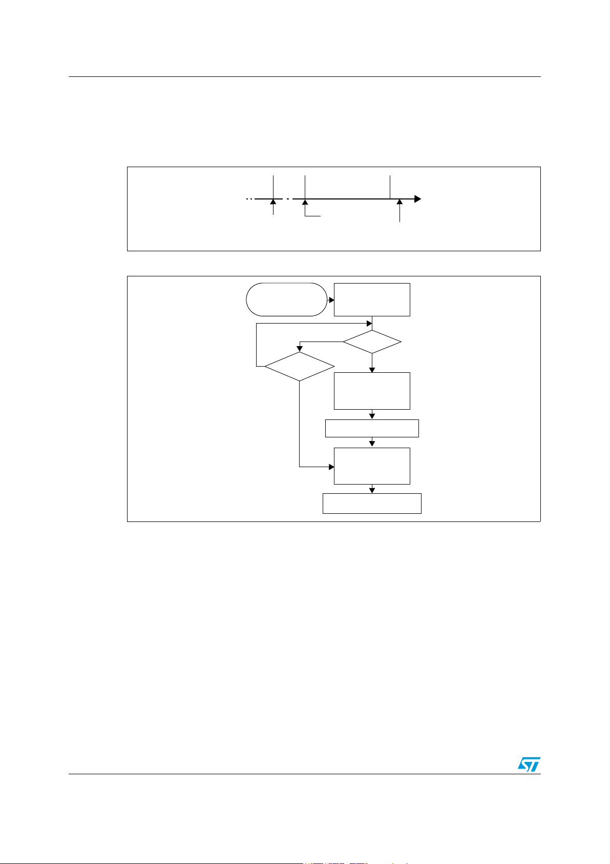
Power saving modes ST72361xx-Auto
HALTRUN RUN
256 OR 4096 CYCLE
DELAY (AFTER RESET)
RESET
OR
INTERRUPT
HALT
INSTRUCTION
FETCH
VECTOR
ACTIVE
(Active Halt enabled)
HALT INSTRUCTION
RESET
INTERRUPT
3)
Y
N
N
Y
CPU
OSCILLATOR
PERIPHERALS
2)
I[1:0] BITS
ON
OFF
10
OFF
FETCH RESET VECTOR
OR SERVICE INTERRUPT
CPU
OSCILLATOR
PERIPHERALS
I[1:0] BITS
ON
OFF
XX
4)
ON
CPU
OSCILLATOR
PERIPHERALS
I[1:0] BITS
ON
ON
XX
4)
ON
256 OR 4096 CPU CLOCK
CYCLE DELAY
(MCCSR.OIE=1)
(AWUCSR.AWUEN=0)
Note: As soon as active halt is enabled, executing a HALT instruction while the Watchdog is active
does not generate a RESET.
This means that the device cannot spend more than a defined delay in this power saving
mode.
Figure 27. ACTIVE HALT timing overview
Figure 28. ACTIVE HALT mode flow-chart
Note: 1 This delay occurs only if the MCU exits ACTIVE HALT mode by means of a RESET.
2 Peripheral clocked with an external clock source can still be active.
3 Only the RTC interrupt and some specific interrupts can exit the MCU from ACTIVE HALT
mode (such as external interrupt). Refer to Tab le 1 6 for more details.
4 Before servicing an interrupt, the CC register is pushed on the stack. The I[1:0] bits in the
CC register are set to the current software priority level of the interrupt routine and restored
when the CC register is popped.
7.6 Auto wake-up from halt mode
Auto Wake-Up From Halt (AWUFH) mode is similar to Halt mode with the addition of an
internal RC oscillator for wake-up. Compared to ACTIVE HALT mode, AWUFH has lower
power consumption because the main clock is not kept running, but there is no accurate
realtime clock available.
66/279 Doc ID 12468 Rev 3
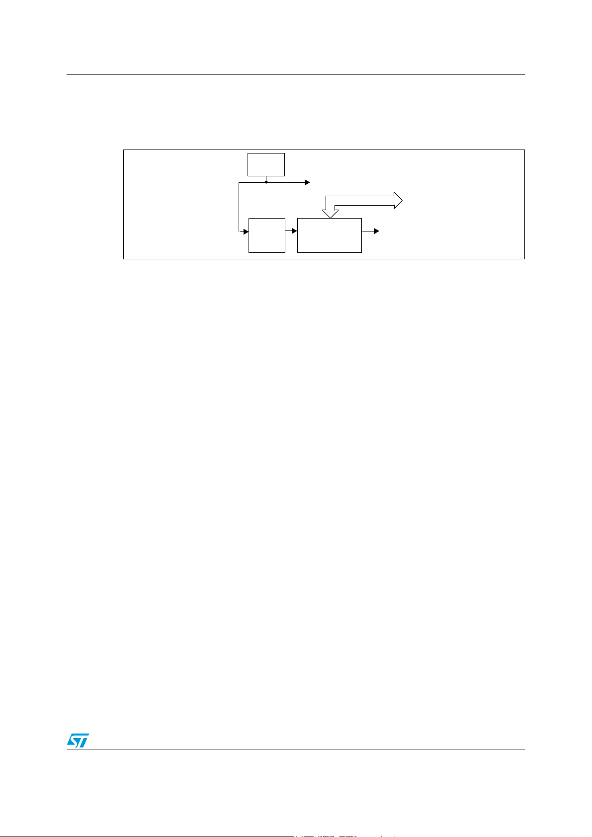
ST72361xx-Auto Power saving modes
AWU RC
AWUFH
f
AWU_RC
AWUFH
(ei0 source)
oscillator
prescaler
interrupt
/64
divider
to Timer input capture
/1 .. 255
It is entered by executing the HALT instruction when the AWUEN bit in the AWUCSR
register has been set and the OIE bit in the MCCSR register is cleared (see Section 10:
Main clock controller with real time clock MCC/RTC for more details).
Figure 29. AWUFH mode block diagram
As soon as HALT mode is entered, and if the AWUEN bit has been set in the AWUCSR
register, the AWU RC oscillator provides a clock signal (f
AWU_RC
). Its frequency is divided by
a fixed divider and a programmable prescaler controlled by the AWUPR register. The output
of this prescaler provides the delay time. When the delay has elapsed the AWUF flag is set
by hardware and an interrupt wakes up the MCU from Halt mode. At the same time the main
oscillator is immediately turned on and a 256 or 4096 cycle delay is used to stabilize it. After
this start-up delay, the CPU resumes operation by servicing the AWUFH interrupt. The AWU
flag and its associated interrupt are cleared by software reading the AWUCSR register.
To compensate for any frequency dispersion of the AWU RC oscillator, it can be calibrated
by measuring the clock frequency f
AWU_RC
and then calculating the right prescaler value.
Measurement mode is enabled by setting the AWUM bit in the AWUCSR register in Run
mode. This connects f
be measured
using the main oscillator clock as a reference time base.
AWU_R C
to the ICAP1 input of the 16-bit timer, allowing the f
AWU_RC
to
Similarities with halt mode
The following AWUFH mode behavior is the same as normal Halt mode:
● The MCU can exit AWUFH mode by means of any interrupt with exit from Halt
capability or a reset (see Section 7.4: Halt mode).
● When entering AWUFH mode, the I[1:0] bits in the CC register are forced to 10b to
enable interrupts. Therefore, if an interrupt is pending, the MCU wakes up immediately.
● In AWUFH mode, the main oscillator is turned off causing all internal processing to be
stopped, including the operation of the on-chip peripherals. None of the peripherals are
clocked except those which get their clock supply from another clock generator (such
as an external or auxiliary oscillator like the AWU oscillator).
● The compatibility of Watchdog operation with AWUFH mode is configured by the
WDGHALT option bit in the option byte. Depending on this setting, the HALT instruction
when executed while the Watchdog system is enabled, can generate a Watchdog
RESET.
Doc ID 12468 Rev 3 67/279

Power saving modes ST72361xx-Auto
AWUFH interrupt
f
CPU
RUN MODE HALT MODE 256 or 4096 t
CPU
RUN MODE
f
AWU_RC
Clear
by software
t
AWU
RESET
INTERRUPT
3)
Y
N
N
Y
CPU
MAIN OSC
PERIPHERALS
2)
I[1:0] BITS
OFF
OFF
10
OFF
FETCH RESET VECTOR
OR SERVICE INTERRUPT
CPU
MAIN OSC
PERIPHERALS
I[1:0] BITS
ON
OFF
XX
4)
ON
CPU
MAIN OSC
PERIPHERALS
I[1:0] BITS
ON
ON
XX
4)
ON
256 OR 4096 CPU CLOCK
DELAY
WATCHDOG
ENABLE
DISABLE
WDGHALT
1)
0
WATCHDOG
RESET
1
CYCLE
AWU RC OSC ON
AWU RC OSC OFF
AWU RC OSC OFF
HALT INSTRUCTION
(MCCSR.OIE=0)
(AWUCSR.AWUEN=1)
Figure 30. AWUF halt timing diagram
Figure 31. AWUFH mode flow-chart
Note: 1 WDGHALT is an option bit. See option byte section for more details.
2 Peripheral clocked with an external clock source can still be active.
3 Only an AWUFH interrupt and some specific interrupts can exit the MCU from HALT mode
(such as external interrupt). Refer to Ta bl e 1 6 for more details.
4 Before servicing an interrupt, the CC register is pushed on the stack. The I[1:0] bits of the
CC register are set to the current software priority level of the interrupt routine and
recovered when the CC register is popped.
68/279 Doc ID 12468 Rev 3

ST72361xx-Auto Power saving modes
7.6.1 Register description
AWUFH control/status register (AWUCSR)
Read/Write (except bit 2 read only)
Reset value: 0000 0000 (00h)
7 0
0 0 0 0 0 AWUF AWUM AWUEN
Bits 7:3 = Reserved.
Bit 2 = AWUF Auto Wake-Up Flag
This bit is set by hardware when the AWU module generates an interrupt and cleared by
software on reading AWUCSR.
0: No AWU interrupt occurred
1: AWU interrupt occurred
Bit 1 = AWUM Auto Wake-Up Measurement
This bit enables the AWU RC oscillator and connects its output to the ICAP1 input of the 16bit timer. This allows the timer to be used to measure the AWU RC oscillator dispersion and
then compensate this dispersion by providing the right value in the AWUPR register.
0: Measurement disabled
1: Measurement enabled
Bit 0 = AWUEN Auto Wake-Up From Halt Enabled
This bit enables the Auto Wake-Up From Halt feature: once HALT mode is entered, the
AWUFH wakes up the microcontroller after a time delay defined by the AWU prescaler
value. It is set and cleared by software.
0: AWUFH (Auto Wake-Up From Halt) mode disabled
1: AWUFH (Auto Wake-Up From Halt) mode enabled
AWUFH prescaler register (AWUPR)
Read/Write
Reset value: 1111 1111 (FFh)
7 0
AWUPR7 AWUPR6 AWUPR5 AWUPR4 AWUPR3 AWUPR2 AWUPR1 AWUPR0
Bits 7:0 = AWUPR[7:0] Auto Wake-Up Prescaler
These 8 bits define the AWUPR Dividing factor as explained below:
Table 23. AWUPR prescaler
AWUPR[7:0] Dividing factor
00h Forbidden (See note)
01h 1
... ...
Doc ID 12468 Rev 3 69/279

Power saving modes ST72361xx-Auto
t
AWU
64 AWUP
1
t
AWURC
---------------------- t
RCSTRT
+=
Table 23. AWUPR prescaler (continued)
AWUPR[7:0] Dividing factor
FEh 254
FFh 255
In AWU mode, the period that the MCU stays in Halt Mode (t
in Figure 30) is defined by
AWU
This prescaler register can be programmed to modify the time that the MCU stays in Halt
mode before waking up automatically.
Note: If 00h is written to AWUPR, depending on the product, an interrupt is generated immediately
after a HALT instruction or the AWUPR remains unchanged.
Table 24. AWU register map and reset values
Address
(Hex.)
002Bh
002Ch
Register
Label
AWUCSR
Reset value
AWUPR
Reset value
76543210
00000
AWUF0AWUM0AWUEN
0
AWUPR71AWUPR61AWUPR51AWUPR41AWUPR31AWUPR21AWUPR11AWUPR0
1
70/279 Doc ID 12468 Rev 3

ST72361xx-Auto I/O ports
8 I/O ports
8.1 Introduction
The I/O ports offer different functional modes:
● transfer of data through digital inputs and outputs
and for specific pins:
● external interrupt generation
● alternate signal input/output for the on-chip peripherals.
An I/O port contains up to 8 pins. Each pin can be programmed independently as digital
input (with or without interrupt generation) or digital output.
8.2 Functional description
Each port has two main registers:
● Data Register (DR)
● Data Direction Register (DDR)
and one optional register:
● Option Register (OR)
Each I/O pin may be programmed using the corresponding register bits in the DDR and OR
registers: Bit X corresponding to pin X of the port. The same correspondence is used for the
DR register.
The following description takes into account the OR register, (for specific ports which do not
provide this register refer to the I/O Port Implementation section). The generic I/O block
diagram is shown in Figure 32
8.2.1 Input modes
The input configuration is selected by clearing the corresponding DDR register bit.
In this case, reading the DR register returns the digital value applied to the external I/O pin.
Different input modes can be selected by software through the OR register.
Note: 1 Writing the DR register modifies the latch value but does not affect the pin status.
2 When switching from input to output mode, the DR register has to be written first to drive the
correct level on the pin as soon as the port is configured as an output.
3 Do not use read/modify/write instructions (BSET or BRES) to modify the DR register as this
might corrupt the DR content for I/Os configured as input.
External interrupt function
When an I/O is configured as Input with Interrupt, an event on this I/O can generate an
external interrupt request to the CPU.
Each pin can independently generate an interrupt request. The interrupt sensitivity is
independently programmable using the sensitivity bits in the EICR register.
Doc ID 12468 Rev 3 71/279

I/O ports ST72361xx-Auto
Each external interrupt vector is linked to a dedicated group of I/O port pins (see pinout
description and interrupt section). If several input pins are selected simultaneously as
interrupt sources, these are first detected according to the sensitivity bits in the EICR
register and then logically ORed.
The external interrupts are hardware interrupts, which means that the request latch (not
accessible directly by the application) is automatically cleared when the corresponding
interrupt vector is fetched. To clear an unwanted pending interrupt by software, the
sensitivity bits in the EICR register must be modified.
8.2.2 Output modes
The output configuration is selected by setting the corresponding DDR register bit. In this
case, writing the DR register applies this digital value to the I/O pin through the latch. Then
reading the DR register returns the previously stored value.
Two different output modes can be selected by software through the OR register: Output
push-pull and open-drain.
Table 25. DR register value and output pin status
DR Push-pull Open-drain
0V
1V
SS
DD
Vss
Floating
8.2.3 Alternate functions
When an on-chip peripheral is configured to use a pin, the alternate function is automatically
selected. This alternate function takes priority over the standard I/O programming.
When the signal is coming from an on-chip peripheral, the I/O pin is automatically
configured in output mode (push-pull or open drain according to the peripheral).
When the signal is going to an on-chip peripheral, the I/O pin must be configured in input
mode. In this case, the pin state is also digitally readable by addressing the DR register.
Note: Input pull-up configuration can cause unexpected value at the input of the alternate
peripheral input. When an on-chip peripheral use a pin as input and output, this pin has to
be configured in input floating mode.
72/279 Doc ID 12468 Rev 3

ST72361xx-Auto I/O ports
DR
DDR
OR
DATA BUS
PAD
V
DD
ALTERNATE
ENABLE
ALTERNATE
OUTPUT
1
0
OR SEL
DDR SEL
DR SEL
PULL-UP
CONDITION
P-BUFFER
(see table below)
N-BUFFER
PULL-UP
(see table below)
1
0
ANALOG
INPUT
If implemented
ALTERNATE
INPUT
V
DD
DIODES
(see table below)
EXTERNAL
SOURCE (eix)
INTERRUPT
CMOS
SCHMITT
TRIGGER
REGISTER
ACCESS
Figure 32. I/O port general block diagram
Table 26. I/O port mode options
Configuration mode Pull-Up P-Buffer
(1)
Diodes
Floating with/without Interrupt Off
Input
Off
Pull-up with/without Interrupt On
On
Push-pull
On
Off
Output
1. NI - not implemented
Note: The diode to VDD is not implemented in the true open drain pads. A local protection between
Off - implemented not activated
On - implemented and activated
the pad and V
Open Drain (logic level) Off
True Open Drain NI NI NI (see note)
is implemented to protect the device against positive stress.
SS
Doc ID 12468 Rev 3 73/279
On
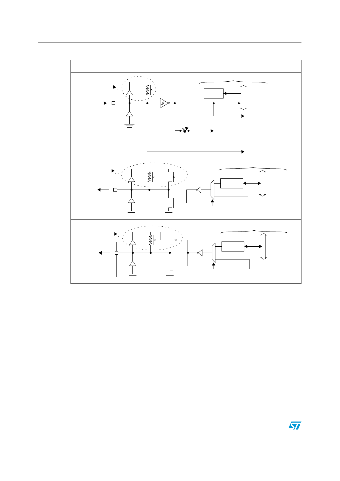
I/O ports ST72361xx-Auto
CONDITION
PAD
V
DD
R
PU
EXTERNAL INTERRUPT
DATA BU S
PULL-UP
INTERRUPT
DR REGISTER ACCESS
W
R
SOURCE (
eix)
DR
REGISTER
CONDITION
ALTERNATE INPUT
NOT IMPLEMENTED IN
TRUE OPEN DRAIN
I/O PORTS
ANALOG INPUT
PAD
R
PU
DATA BU S
DR
DR REGISTER ACCESS
R/W
V
DD
ALTERNATEALTERNATE
ENABLE OUTPUT
REGISTER
NOT IMPLEMENTED IN
TRUE OPEN DRAIN
I/O PORTS
PAD
R
PU
DATA BU S
DR
DR REGISTER ACCESS
R/W
V
DD
ALTERNATEALTERNATE
ENABLE OUTPUT
REGISTER
NOT IMPLEMENTED IN
TRUE OPEN DRAIN
I/O PORTS
Table 27. I/O port configurations
Hardware configuration
(1)
Input
(2)
Open-drain Output
2)
Push-pull Output
1. When the I/O port is in input configuration and the associated alternate function is enabled as an output,
reading the DR register will read the alternate function output status.
2. When the I/O port is in output configuration and the associated alternate function is enabled as an input,
the alternate function reads the pin status given by the DR register content.
Caution: The alternate function must not be activated as long as the pin is configured as input with
interrupt, in order to avoid generating spurious interrupts.
Analog alternate function
When the pin is used as an ADC input, the I/O must be configured as floating input. The
analog multiplexer (controlled by the ADC registers) switches the analog voltage present on
the selected pin to the common analog rail which is connected to the ADC input.
It is recommended not to change the voltage level or loading on any port pin while
conversion is in progress. Furthermore it is recommended not to have clocking pins located
close to a selected analog pin.
74/279 Doc ID 12468 Rev 3
ST72361xx-Auto I/O ports
01
floating/pull-up
interrupt
INPUT
00
floating
(reset state)
INPUT
10
open-drain
OUTPUT
11
push-pull
OUTPUT
XX
= DDR, OR
Warning: The analog input voltage level must be within the limits
stated in the absolute maximum ratings.
8.3 I/O port implementation
The hardware implementation on each I/O port depends on the settings in the DDR and OR
registers and specific feature of the I/O port such as ADC Input or true open drain.
Switching these I/O ports from one state to another should be done in a sequence that
prevents unwanted side effects. Recommended safe transitions are illustrated in Figure 33.
Other transitions are potentially risky and should be avoided, since they are likely to present
unwanted side-effects such as spurious interrupt generation.
Figure 33. Interrupt I/O port state transitions
8.4 I/O port register configurations
The I/O port register configurations are summarized as follows.
8.4.1 Standard ports
Table 28. Configuration of PB7:6, PC0, PC3, PC7:5, PD3:2, PD5, PE7:0, PF7:0
Mode DDR OR
Floating input
Pull-up input 1
Open drain output
Push-pull output 1
0
0
0
1
Doc ID 12468 Rev 3 75/279

I/O ports ST72361xx-Auto
8.4.2 Interrupt ports
Table 29. Configuration of PA0, 2, 4, 6; PB0, 2,4; PC1; PD0,6 (with pull-up)
Mode DDR OR
Floating input
0
0
Pull-up interrupt input 1
Open drain output
0
1
Push-pull output 1
Table 30. Configuration of PA1, 3, 5, 7; PB1,3,5; PC2; PD1, 4, 7 (without pull-up)
Mode DDR OR
Floating input
0
0
Floating interrupt input 1
Open drain output
0
1
Push-pull output 1
76/279 Doc ID 12468 Rev 3

ST72361xx-Auto I/O ports
8.4.3 Pull-up input port
Table 31. Configuration of PC4
Mode
pull-up input
The PC4 port cannot operate as a general purpose output. If DDR = 1 it is still possible to
read the port through the DR register.
Table 32. Port configuration
Input Output
Port Pin name
OR = 0 OR = 1 OR = 0 OR = 1
Por t A
Por t B
Por t C
PA 0
pull-up interrupt (ei0)
PA1 floating interrupt (ei0)
PA2 pull-up interrupt (ei0)
PA3 floating interrupt (ei0)
floating
PA4 pull-up interrupt (ei0)
PA5 floating interrupt (ei0)
PA6 pull-up interrupt (ei0)
PA7 floating interrupt (ei0)
PB0
pull-up interrupt (ei1)
PB1 floating interrupt (ei1)
PB2 pull-up interrupt (ei1)
floating
PB3 floating interrupt (ei1)
PB4 pull-up interrupt (ei1)
PB5 floating interrupt (ei1)
PC0
pull-up
PC1 pull-up interrupt (ei2)
floating
PC2 floating interrupt (ei2)
PC3 pull-up
open drain push-pull
open drain push-pull
open drain push-pull
PC4 pull-up
PC7:5 floating pull-up open drain push-pull
Doc ID 12468 Rev 3 77/279

I/O ports ST72361xx-Auto
Table 32. Port configuration (continued)
Input Output
Port Pin name
OR = 0 OR = 1 OR = 0 OR = 1
PD0
PD1 floating interrupt (ei3)
PD3:2 pull-up
Por t D
Port E PE7:0 floating (TTL) pull-up (TTL) open drain push-pull
Port F PF7:0 floating (TTL) pull-up (TTL) open drain push-pull
PD4 floating interrupt (ei3)
PD5 pull-up
PD6 pull-up interrupt (ei3)
PD7 floating interrupt (ei3)
8.5 Low power modes
Table 33. Effect of low power modes on I/O ports
Mode Description
WAIT No effect on I/O ports. External interrupts cause the device to exit from WAIT mode.
HALT No effect on I/O ports. External interrupts cause the device to exit from HALT mode.
floating
pull-up interrupt (ei3)
open drain push-pull
8.6 Interrupts
The external interrupt event generates an interrupt if the corresponding configuration is
selected with DDR and OR registers and the interrupt mask in the CC register is not active
(RIM instruction).
Table 34. I/O port interrupt control/wake-up capability
Interrupt event
External interrupt on selected
external event
Event
flag
-
Enable
control
bit
DDRx
ORx
Exit
from
wait
Exit
from
halt
Ye s
78/279 Doc ID 12468 Rev 3

ST72361xx-Auto I/O ports
Table 35. I/O port register map and reset values
Address
(Hex.)
Register
label
Reset value
of all IO port registers
0000h PADR
0002h PAOR
0003h PBDR
0005h PBOR
0006h PCDR
0008h PCOR
0009h PDDR
000Bh PDOR
000Ch PEDR
76543210
000 00000
MSB LSB0001h PADDR
MSB LSB0004h PBDDR
MSB LSB0007h PCDDR
MSB LSB000Ah PDDDR
MSB LSB000Dh PEDDR
000Eh PEOR
000Fh PFDR
0011h PFOR
MSB LSB0010h PFDDR
Doc ID 12468 Rev 3 79/279

Window watchdog (WWDG) ST72361xx-Auto
9 Window watchdog (WWDG)
9.1 Introduction
The Window Watchdog is used to detect the occurrence of a software fault, usually
generated by external interference or by unforeseen logical conditions, which causes the
application program to abandon its normal sequence. The Watchdog circuit generates an
MCU reset on expiry of a programmed time period, unless the program refreshes the
contents of the downcounter before the T6 bit becomes cleared. An MCU reset is also
generated if the 7-bit downcounter value (in the control register) is refreshed before the
downcounter has reached the window register value. This implies that the counter must be
refreshed in a limited window.
9.2 Main features
● Programmable free-running down counter
● Conditional reset
– Reset (if watchdog activated) when the downcounter value becomes less than 40h
– Reset (if watchdog activated) if the downcounter is reloaded outside the window
(see Figure 37)
● Hardware/Software Watchdog activation (selectable by option byte)
● Optional reset on HALT instruction (configurable by option byte)
9.3 Functional description
The counter value stored in the WDGCR register (bits T[6:0]), is decremented every 16384
f
cycles (approx.), and the length of the timeout period can be programmed by the user
OSC2
in 64 increments.
If the watchdog is activated (the WDGA bit is set) and when the 7-bit downcounter (T[6:0]
bits) rolls over from 40h to 3Fh (T6 becomes cleared), it initiates a reset cycle pulling low the
reset pin for typically 30µs. If the software reloads the counter while the counter is greater
than the value stored in the window register, then a reset is generated.
80/279 Doc ID 12468 Rev 3
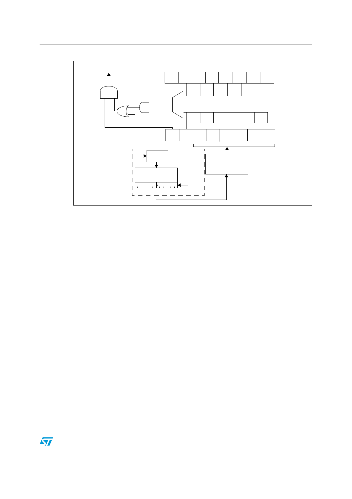
ST72361xx-Auto Window watchdog (WWDG)
RESET
WDGA
6-BIT DOWNCOUNTER (CNT)
T6
T0
WATCHDOG CONTROL REGISTER (WDGCR)
T1
T2
T3
T4
T5
-
W6
W0
WATCHDOG WINDOW REGISTER (WDGWR)
W1
W2
W3
W4
W5
comparator
T6:0 > W6:0
CMP
= 1 when
Write WDGCR
WDG PRESCALER
DIV 4
f
OSC2
12-BIT MCC
RTC COUNTER
MSB
LSB
DIV 64
0
5
6
11
MCC/RTC
TB[1:0] bits
(MCCSR
Register)
Figure 34. Watchdog block diagram
The application program must write in the WDGCR register at regular intervals during
normal operation to prevent an MCU reset. This operation must occur only when the counter
value is lower than the window register value. The value to be stored in the WDGCR register
must be between FFh and C0h (see Figure 35):
● Enabling the watchdog:
when Software Watchdog is selected (by option byte), the watchdog is disabled after a
reset. It is enabled by setting the WDGA bit in the WDGCR register, then it cannot be
disabled again except by a reset.
When Hardware Watchdog is selected (by option byte), the watchdog is always active
and the WDGA bit is not used.
● Controlling the downcounter:
this downcounter is free-running: It counts down even if the watchdog is disabled.
When the watchdog is enabled, the T6 bit must be set to prevent generating an
immediate reset.
The T[5:0] bits contain the number of increments which represents the time delay
before the watchdog produces a reset (see Figure 35). The timing varies between a
minimum and a maximum value due to the unknown status of the prescaler when
writing to the WDGCR register (see Figure 36).
The window register (WDGWR) contains the high limit of the window: To prevent a
reset, the downcounter must be reloaded when its value is lower than the window
register value and greater than 3Fh. Figure 37 describes the window watchdog
process.
Note: The T6 bit can be used to generate a software reset (the WDGA bit is set and the T6 bit is
cleared).
● Watchdog Reset on Halt option:
if the watchdog is activated and the watchdog reset on halt option is selected, then the
HALT instruction will generate a Reset.
Doc ID 12468 Rev 3 81/279

Window watchdog (WWDG) ST72361xx-Auto
CNT Value (hex.)
Watchdog timeout (ms) @ 8 MHz f
OSC2
3F
00
38
128
1.5 65
30
28
20
18
10
08
503418 82 98 114
9.4 Using halt mode with the WDG
If Halt mode with Watchdog is enabled by option byte (no watchdog reset on HALT
instruction), it is recommended before executing the HALT instruction to refresh the WDG
counter, to avoid an unexpected WDG reset immediately after waking up the microcontroller.
9.5 How to program the watchdog timeout
Figure 35 shows the linear relationship between the 6-bit value to be loaded in the
Watchdog Counter (CNT) and the resulting timeout duration in milliseconds. This can be
used for a quick calculation without taking the timing variations into account. If more
precision is needed, use the formulae in Figure 36.
Caution: When writing to the WDGCR register, always write 1 in the T6 bit to avoid generating an
immediate reset.
Figure 35. Approximate timeout duration
82/279 Doc ID 12468 Rev 3
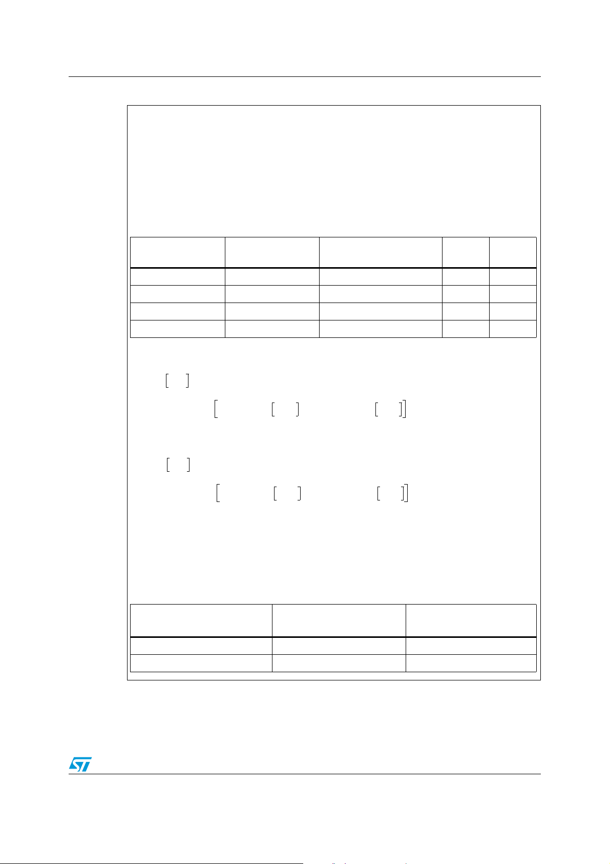
ST72361xx-Auto Window watchdog (WWDG)
WHERE:
t
min0
= (LSB + 128) x 64 x t
OSC2
t
max0
= 16384 x t
OSC2
t
OSC2
= 125ns if f
OSC2
=8 MHz
CNT = Value of T[5:0] bits in the WDGCR register (6 bits)
MSB and LSB are values from the table below depending on the timebase selected by the
TB[1:0] bits in the MCCSR register
To calculate the minimum watchdog timeout (t
min
):
IF THEN
ELSE
To calculate the maximum Watchdog Timeout (t
max
):
IF THEN
ELSE
Note: In the above formulae, division results must be rounded down to the next
integer value.
Example 1:
With 2ms timeout selected in MCCSR register
TB1 Bit
(MCCSR Reg.)
TB0 Bit
(MCCSR Reg.)
Selected MCCSR timebase MSB LSB
002ms 459
014ms 853
1 0 10ms 20 35
1 1 25ms 49 54
Value of T[5:0] bits in WDGCR
register (Hex.)
Min. watchdog timeout (ms)
t
min
Max. watchdog timeout (ms)
t
max
00 1.496 2.048
3F 128 128.552
CNT
MSB
4
-------------
<
t
mintmin0
16384 CN T t
osc2
+=
t
mintmin0
16384 C NT
4CNT
MSB
-----------------
–
192 LSB+64
4CNT
MSB
-----------------
+ t
osc2
+=
CNT
MSB
4
-------------
t
maxtmax0
16384 CN T t
osc2
+=
t
maxtmax0
16384 C NT
4CNT
MSB
-----------------
–
192 L SB+64
4CNT
MSB
-----------------
+ t
osc2
+=
Figure 36. Exact timeout duration (t
min
and t
max
)
Doc ID 12468 Rev 3 83/279

Window watchdog (WWDG) ST72361xx-Auto
T6 bit
Reset
WDGWR
T[5:0] CNT downcounter
time
Refresh WindowRefresh not allowed
(step = 16384/f
OSC2
)
3Fh
Figure 37. Window watchdog timing diagram
9.6 Low power modes
Table 36. Effect of low power modes on WDG
Mode Description
SLOW No effect on Watchdog: the downcounter continues to decrement at normal speed.
WAIT No effect on Watchdog: the downcounter continues to decrement.
OIE bit in
MCCSR
register
WDGHALT
bit in Option
Byte
No Watchdog reset is generated. The MCU enters Halt mode. The
Watchdog counter is decremented once and then stops counting and is
no longer able to generate a watchdog reset until the MCU receives an
HALT
00
external interrupt or a reset.
If an interrupt is received (refer to interrupt table mapping to see
interrupts which can occur in halt mode), the Watchdog restarts counting
after 256 or 4096 CPU clocks. If a reset is generated, the Watchdog is
disabled (reset state) unless Hardware Watchdog is selected by option
byte. For application recommendations see Section 9.8: Using halt
mode with the WDG (WDGHALT option) below.
0 1 A reset is generated instead of entering halt mode.
No reset is generated. The MCU enters Active Halt mode. The
ACTIVE
HALT
1x
Watchdog counter is not decremented. It stop counting. When the MCU
receives an oscillator interrupt or external interrupt, the Watchdog
restarts counting immediately. When the MCU receives a reset the
Watchdog restarts counting after 256 or 4096 CPU clocks.
9.7 Hardware watchdog option
If Hardware Watchdog is selected by option byte, the watchdog is always active and the
WDGA bit in the WDGCR is not used. Refer to the Option Byte description.
84/279 Doc ID 12468 Rev 3

ST72361xx-Auto Window watchdog (WWDG)
9.8 Using halt mode with the WDG (WDGHALT option)
The following recommendation applies if Halt mode is used when the watchdog is enabled.
● Before executing the HALT instruction, refresh the WDG counter, to avoid an
unexpected WDG reset immediately after waking up the microcontroller.
9.9 Interrupts
None.
9.10 Register description
9.10.1 Control register (WDGCR)
Read/Write
Reset value: 0111 1111 (7Fh)
7 0
WDGA T6 T5 T4 T3 T2 T1 T0
Bit 7 = WDGA Activation bit.
This bit is set by software and only cleared by hardware after a reset. When WDGA = 1, the
watchdog can generate a reset.
0: Watchdog disabled
1: Watchdog enabled
Note: This bit is not used if the hardware watchdog option is enabled by option byte.
Bits 6:0 = T[6:0] 7-bit counter (MSB to LSB).
These bits contain the value of the watchdog counter. It is decremented every 16384 f
cycles (approx.). A reset is produced when it rolls over from 40h to 3Fh (T6 becomes
cleared).
9.10.2 Window Register (WDGWR)
Read/ write
Reset value: 0111 1111 (7Fh)
7 0
- W6W5 W4W3W2W1W0
Bit 7 = Reserved
Bits 6:0 = W[6:0] 7-bit window value
These bits contain the window value to be compared to the downcounter.
OSC2
Doc ID 12468 Rev 3 85/279

Window watchdog (WWDG) ST72361xx-Auto
Table 37. Watchdog timer register map and reset values
Address
(Hex.)
2F
30
Register label 7 6543210
WDGCR
Reset value
WDGWR
Reset value
WDGA0T61T51T41T31T21T11T0
-
W61W51W41W31W21W11W0
0
1
1
86/279 Doc ID 12468 Rev 3

ST72361xx-Auto Main clock controller with real time clock MCC/RTC
DIV 2, 4, 8, 16
MCC/RTC INTERRUPT
SMSCP1 CP0 TB1 TB0 OIE OIF
CPU CLOCK
MCCSR
RTC
COUNTER
TO CPU AND
PERIPHERALS
f
OSC2
f
CPU
MCO
MCO
TO
WATCHDOG
TIMER
10 Main clock controller with real time clock MCC/RTC
The Main Clock Controller consists of three different functions:
●
a programmable CPU clock prescaler
●
a clock-out signal to supply external devices
●
a real time clock timer with interrupt capability
Each function can be used independently and simultaneously.
10.1
10.2
10.3
Programmable CPU clock prescaler
The programmable CPU clock prescaler supplies the clock for the ST7 CPU and its internal
peripherals. It manages SLOW power saving mode (See Section 7.2: Slow mode for more
details).
The prescaler selects the f
main clock frequency and is controlled by three bits in the
CPU
MCCSR register: CP[1:0] and SMS.
Clock-out capability
The clock-out capability is an alternate function of an I/O port pin that outputs a f
to drive external devices. It is controlled by the MCO bit in the MCCSR register.
OSC2
clock
Real time clock timer (RTC)
The counter of the real time clock timer allows an interrupt to be generated based on an
accurate real time clock. Four different time bases depending directly on f
The whole functionality is controlled by 4 bits of the MCCSR register: TB[1:0], OIE and OIF.
When the RTC interrupt is enabled (OIE bit set), the ST7 enters ACTIVE HALT mode when
the HALT instruction is executed. See Section 7.5: Active halt mode for more details.
Figure 38. Main clock controller (MCC/RTC) block diagram
are available.
OSC2
Doc ID 12468 Rev 3 87/279

Main clock controller with real time clock MCC/RTC ST72361xx-Auto
10.4
Table 38. Effect of low power modes on MCC/RTC
WAIT
ACTIVE HALT
HALT
and
AWUF HALT
10.5
Low power modes
Mode Description
No effect on MCC/RTC peripheral.
MCC/RTC interrupt cause the device to exit from WAIT mode.
No effect on MCC/RTC counter (OIE bit is set), the registers are frozen.
MCC/RTC interrupt cause the device to exit from ACTIVE HALT mode.
MCC/RTC counter and registers are frozen.
MCC/RTC operation resumes when the MCU is woken up by an interrupt with “exit from
HALT” capability.
Interrupts
The MCC/RTC interrupt event generates an interrupt if the OIE bit of the MCCSR register is
set and the interrupt mask in the CC register is not active (RIM instruction).
Table 39. MCC/RTC Interrupt control wake-up capability
Interrupt event
Time base overflow event OIF OIE Yes No
Event
flag
Enable
control
bit
Exit
from
wait
Exit
from
halt
1)
Note: The MCC/RTC interrupt wakes up the MCU from ACTIVE HALT mode, not from HALT or
AWUF HALT mode.
10.6
Register description
10.6.1 MCC control/status register (MCCSR)
Read/Write
Reset value: 0000 0000 (00h)
7 0
MCO CP1 CP0 SMS TB1 TB0 OIE OIF
Bit 7 = MCO Main clock out selection
This bit enables the MCO alternate function on the corresponding I/O port. It is set and
cleared by software.
0: MCO alternate function disabled (I/O pin free for general-purpose I/O)
1: MCO alternate function enabled (f
Bits 6:5 = CP[1:0] CPU clock prescaler
These bits select the CPU clock prescaler which is applied in the different slow modes. Their
action is conditioned by the setting of the SMS bit. These two bits are set and cleared by
software
OSC2
on I/O port)
88/279 Doc ID 12468 Rev 3
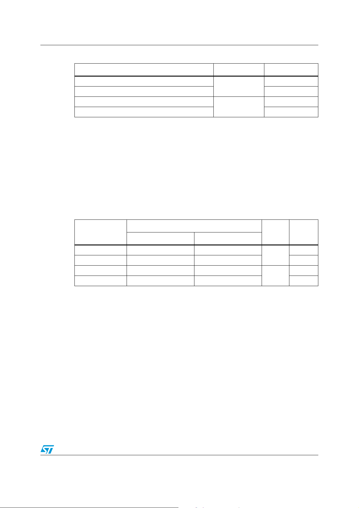
ST72361xx-Auto Main clock controller with real time clock MCC/RTC
Table 40. CPU clock frequency in SLOW mode
f
in SLOW mode CP1 CP0
CPU
f
/ 2
OSC2
/ 4 1
f
OSC2
/ 8
f
OSC2
f
/ 16 1
OSC2
0
1
0
0
Bit 4 = SMS Slow mode select
This bit is set and cleared by software.
0: Normal mode. f
1: Slow mode. f
= f
CPU
CPU
OSC2
is given by CP1, CP0
See Section 7.2: Slow mode and Section 10: Main clock controller with real time clock
MCC/RTC for more details.
Bits 3:2 = TB[1:0] Time base control
These bits select the programmable divider time base. They are set and cleared by
software.
Table 41. Time base selection
Time base
Counter prescaler
=4 MHz f
f
OSC2
16000 4ms 2ms
OSC2
=8 MHz
TB1 TB0
0
0
32000 8ms 4ms 1
80000 20ms 10ms
0
1
200000 50ms 25ms 1
A modification of the time base is taken into account at the end of the current period
(previously set) to avoid an unwanted time shift. This allows to use this time base as a real
time clock.
Bit 1 = OIE Oscillator interrupt enable
This bit set and cleared by software.
0: Oscillator interrupt disabled
1: Oscillator interrupt enabled
This interrupt can be used to exit from ACTIVE HALT mode.
When this bit is set, calling the ST7 software HALT instruction enters the ACTIVE HALT
power saving mode
.
Bit 0 = OIF Oscillator interrupt flag
This bit is set by hardware and cleared by software reading the CSR register. It indicates
when set that the main oscillator has reached the selected elapsed time (TB1:0).
0: Timeout not reached
1: Timeout reached
Doc ID 12468 Rev 3 89/279

Main clock controller with real time clock MCC/RTC ST72361xx-Auto
Caution:
The BRES and BSET instructions must not be used on the MCCSR register to avoid
unintentionally clearing the OIF bit.
Table 42. Main clock controller register map and reset values
Address
(Hex.)
002Dh
002Eh
Register
label
SICSR
Reset value
MCCSR
Reset value
76543210
0 AVDIE AVDF LVDRF 0
MCO0CP1
0
CP0
0
SMS
0
TB1
0
00
TB0
0
OIE
0
WDGRF
x
OIF
0
90/279 Doc ID 12468 Rev 3
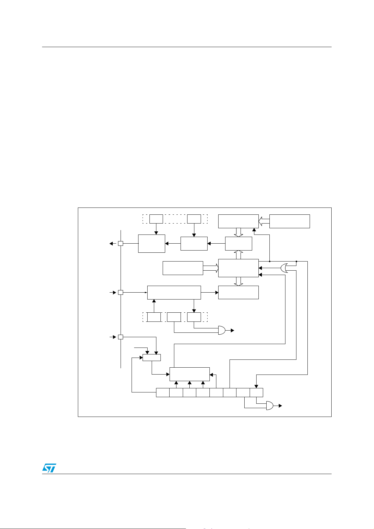
ST72361xx-Auto PWM auto-reload timer (ART)
OVF INTERRUPT
EXCL CC2 CC1 CC0 TCE FCRL OIE OVF
ARTCSR
f
INPUT
PWMx
PORT
FUNCTION
ALTERNATE
OCRx
COMPARE
REGISTER
PROGRAMMABLE
PRESCALER
8-BIT COUNTER
(CAR REGISTER)
ARR
REGISTER
ICRx
REGISTER
LOAD
OPx
POLARITY
CONTROL
OEx
PWMCR
MUX
f
CPU
DCRx
REGISTER
LOAD
f
COUNTER
ARTCLK
f
EXT
ARTICx
ICFxICSx
ICCSR
LOAD
ICx INTERRUPT
ICIEx
INPUT CAPTURE
CONTROL
11 PWM auto-reload timer (ART)
11.1 Introduction
The Pulse Width Modulated Auto-Reload Timer on-chip peripheral consists of an 8-bit autoreload counter with compare/capture capabilities and of a 7-bit prescaler clock source.
These resources allow five possible operating modes:
● Generation of up to four independent PWM signals
● Output compare and Time base interrupt
● Up to two input capture functions
● External event detector
● Up to two external interrupt sources
The three first modes can be used together with a single counter frequency.
The timer can be used to wake up the MCU from WAIT and HALT modes.
Figure 39. PWM auto-reload timer block diagram
Doc ID 12468 Rev 3 91/279

PWM auto-reload timer (ART) ST72361xx-Auto
11.2 Functional description
11.2.1 Counter
The free running 8-bit counter is fed by the output of the prescaler, and is incremented on
every rising edge of the clock signal.
It is possible to read or write the contents of the counter on the fly by reading or writing the
Counter Access register (ARTCAR).
When a counter overflow occurs, the counter is automatically reloaded with the contents of
the ARTARR register (the prescaler is not affected).
11.2.2 Counter clock and prescaler
The counter clock frequency is given by:
f
COUNTER
= f
INPUT
The timer counter’s input clock (f
selects one of the eight available taps of the prescaler, as defined by CC[2:0] bits in the
Control/Status Register (ARTCSR). Thus the division factor of the prescaler can be set to 2
(where n = 0, 1...7).
/ 2
CC[2:0]
) feeds the 7-bit programmable prescaler, which
INPUT
n
This f
can be either the f
frequency source is selected through the EXCL bit of the ARTCSR register and
INPUT
or an external input frequency f
CPU
The clock input to the counter is enabled by the TCE (Timer Counter Enable) bit in the
ARTCSR register. When TCE is reset, the counter is stopped and the prescaler and counter
contents are frozen. When TCE is set, the counter runs at the rate of the selected clock
source.
11.2.3 Counter and prescaler Initialization
After RESET, the counter and the prescaler are cleared and f
The counter can be initialized by:
● Writing to the ARTARR register and then setting the FCRL (Force Counter Re-Load)
and the TCE (Timer Counter Enable) bits in the ARTCSR register.
● Writing to the ARTCAR counter access register,
In both cases the 7-bit prescaler is also cleared, whereupon counting will start from a known
value.
Direct access to the prescaler is not possible.
11.2.4 Output compare control
The timer compare function is based on four different comparisons with the counter (one for
each PWMx output). Each comparison is made between the counter value and an output
compare register (OCRx) value. This OCRx register can not be accessed directly, it is
loaded from the duty cycle register (PWMDCRx) at each overflow of the counter.
EXT
.
INPUT
= f
CPU
.
This double buffering method avoids glitch generation when changing the duty cycle on the
fly.
92/279 Doc ID 12468 Rev 3

ST72361xx-Auto PWM auto-reload timer (ART)
COUNTER
FDh FEh FFh FDh FEh FFh FDh FEh
ARTARR=FDh
f
COUNTER
OCRx
PWMDCRx
FDh
FEh
FDh
FEh
FFh
PWMx
DUTY CYCLE
REGISTER
AUTO-RELOAD
REGISTER
PWMx OUTPUT
t
255
000
WITH OEx=1
AND OPx=0
(ARTARR)
(PWMDCRx)
WITH OEx=1
AND OPx=1
COUNTER
Figure 40. Output compare control
11.2.5 Independent PWM signal generation
This mode allows up to four Pulse Width Modulated signals to be generated on the PWMx
output pins with minimum core processing overhead. This function is stopped during HALT
mode.
Each PWMx output signal can be selected independently using the corresponding OEx bit
in the PWM Control register (PWMCR). When this bit is set, the corresponding I/O pin is
configured as output push-pull alternate function.
The PWM signals all have the same frequency which is controlled by the counter period and
the ARTARR register value.
f
PWM
= f
COUNTER
/ (256 - ARTARR)
When a counter overflow occurs, the PWMx pin level is changed depending on the
corresponding OPx (output polarity) bit in the PWMCR register. When the counter reaches
the value contained in one of the output compare register (OCRx) the corresponding PWMx
pin level is restored.
It should be noted that the reload values will also affect the value and the resolution of the
duty cycle of the PWM output signal. To obtain a signal on a PWMx pin, the contents of the
OCRx register must be greater than the contents of the ARTARR register.
The maximum available resolution for the PWMx duty cycle is:
Resolution = 1 / (256 - ARTARR)
Note: To have the maximum resolution (1/256), the ARTARR register must be 0. With this
maximum resolution, 0% and 100% can be obtained by changing the polarity.
Figure 41. PWM auto-reload timer function
Doc ID 12468 Rev 3 93/279
PWM auto-reload timer (ART) ST72361xx-Auto
COUNTER
PWMx OUTPUT
t
WITH OEx=1
AND OPx=0
FDh FEh FFh FDh FEh FFh FDh FEh
OCRx=FCh
OCRx=FDh
OCRx=FEh
OCRx=FFh
ARTARR
f
COUNTER
=FDh
COUNTER
t
FDh FEh FFh FDh
OVF
ARTCSR READ
INTERRUPT
ARTARR
f
EXT=fCOUNTER
FEh FFh FDh
IF OIE = 1
INTERRUPT
IF OIE = 1
ARTCSR READ
=FDh
Figure 42. PWM signal from 0% to 100% duty cycle
11.2.6 Output compare and Time base interrupt
On overflow, the OVF flag of the ARTCSR register is set and an overflow interrupt request is
generated if the overflow interrupt enable bit, OIE, in the ARTCSR register, is set. The OVF
flag must be reset by the user software. This interrupt can be used as a time base in the
application.
11.2.7 External clock and event detector mode
Using the f
external prescaler input clock, the auto-reload timer can be used as an
EXT
external clock event detector. In this mode, the ARTARR register is used to select the
n
n
number of events to be counted before setting the OVF flag.
EVENT
= 256 - ARTARR
EVENT
Caution: The external clock function is not available in HALT mode. If HALT mode is used in the
application, prior to executing the HALT instruction, the counter must be disabled by clearing
the TCE bit in the ARTCSR register to avoid spurious counter increments.
Figure 43. External event detector example (3 counts)
11.2.8 Input capture function
Input Capture mode allows the measurement of external signal pulse widths through
ARTICRx registers.
94/279 Doc ID 12468 Rev 3

ST72361xx-Auto PWM auto-reload timer (ART)
04h
COUNTER
t
01h
f
COUNTER
xxh
02h 03h 05h 06h 07h
05h
ARTICx PIN
CFx FLAG
ICAP SAMPLED
INTERRUPT
f
CPU
ICAP SAMPLED
Each input capture can generate an interrupt independently on a selected input signal
transition. This event is flagged by a set of the corresponding CFx bits of the Input Capture
Control/Status register (ARTICCSR).
These input capture interrupts are enabled through the CIEx bits of the ARTICCSR register.
The active transition (falling or rising edge) is software programmable through the CSx bits
of the ARTICCSR register.
The read only input capture registers (ARTICRx) are used to latch the auto-reload counter
value when a transition is detected on the ARTICx pin (CFx bit set in ARTICCSR register).
After fetching the interrupt vector, the CFx flags can be read to identify the interrupt source.
Note: After a capture detection, data transfer in the ARTICRx register is inhibited until the next
read (clearing the CFx bit).
The timer interrupt remains pending while the CFx flag is set when the interrupt is enabled
(CIEx bit set). This means, the ARTICRx register has to be read at each capture event to
clear the CFx flag.
The timing resolution is given by auto-reload counter cycle time (1/f
COUNTER
).
Note: During HALT mode, input capture is inhibited (the ARTICRx is never reloaded) and only the
external interrupt capability can be used.
The ARTICx signal is synchronized on CPU clock. It takes two rising edges until ARTICRx is
latched with the counter value. Depending on the prescaler value and the time when the
ICAP event occurs, the value loaded in the ARTICRx register may be different.
If the counter is clocked with the CPU clock, the value latched in ARTICRx is always the next
counter value after the event on ARTICx occurred (Figure 44).
If the counter clock is prescaled, it depends on the position of the ARTICx event within the
counter cycle (Figure 45).
Figure 44. Input capture timing diagram, f
COUNTER
= f
CPU
Doc ID 12468 Rev 3 95/279

PWM auto-reload timer (ART) ST72361xx-Auto
04h
COUNTER
t
f
COUNTER
xxh
03h
04h
ARTICx PIN
CFx FLAG
ICRx REGISTER
INTERRUPT
f
CPU
ICAP SAMPLED
05h
04h
COUNTER
t
f
COUNTER
xxh
03h
05h
ARTICx PIN
CFx FLAG
ICRx REGISTER
INTERRUPT
f
CPU
ICAP SAMPLED
05h
ARTICx PIN
CFx FLAG
t
INTERRUPT
Figure 45. Input capture timing diagram, f
COUNTER
= f
CPU
/ 4
11.2.9 External interrupt capability
This mode allows the Input capture capabilities to be used as external interrupt sources.
The interrupts are generated on the edge of the ARTICx signal.
The edge sensitivity of the external interrupts is programmable (CSx bit of ARTICCSR
register) and they are independently enabled through CIEx bits of the ARTICCSR register.
After fetching the interrupt vector, the CFx flags can be read to identify the interrupt source.
During HALT mode, the external interrupts can be used to wake up the micro (if the CIEx bit
is set). In this case, the interrupt synchronization is done directly on the ARTICx pin edge
(Figure 46).
Figure 46. ART external interrupt in halt mode
96/279 Doc ID 12468 Rev 3

ST72361xx-Auto PWM auto-reload timer (ART)
11.3 Register description
Control/status register (ARTCSR)
Read/Write
Reset value: 0000 0000 (00h)
7 0
EXCL CC2 CC1 CC0 TCE FCRL OIE OVF
Bit 7 = EXCL External Clock
This bit is set and cleared by software. It selects the input clock for the 7-bit prescaler.
0: CPU clock.
1: External clock.
Bit 6:4 = CC[2:0] Counter Clock Control
These bits are set and cleared by software. They determine the prescaler division ratio from
f
.
INPUT
Table 43. Counter clock control
f
COUNTER
f
INPUT
f
INPUT
f
INPUT
f
INPUT
f
INPUT
f
INPUT
f
INPUT
f
INPUT
/ 2
/ 4
/ 8
/ 16
/ 32
/ 64
/ 128
With f
=8 MHz CC2 CC1 CC0
INPUT
8 MHz
4 MHz
2 MHz
1 MHz
500 kHz
250 kHz
125 kHz
62.5 kHz
0
0
0
0
1
1
1
1
0
0
1
1
0
0
1
1
0
1
0
1
0
1
0
1
Bit 3 = TCE Timer Counter Enable
This bit is set and cleared by software. It puts the timer in the lowest power consumption
mode.
0: Counter stopped (prescaler and counter frozen).
1: Counter running.
Bit 2 = FCRL
Force Counter Re-Load
This bit is write-only and any attempt to read it will yield a logical zero. When set, it causes
the contents of ARTARR register to be loaded into the counter, and the content of the
prescaler register to be cleared in order to initialize the timer before starting to count.
Bit 1 = OIE
Overflow Interrupt Enable
This bit is set and cleared by software. It allows to enable/disable the interrupt which is
generated when the OVF bit is set.
0: Overflow Interrupt disable.
1: Overflow Interrupt enable.
Doc ID 12468 Rev 3 97/279
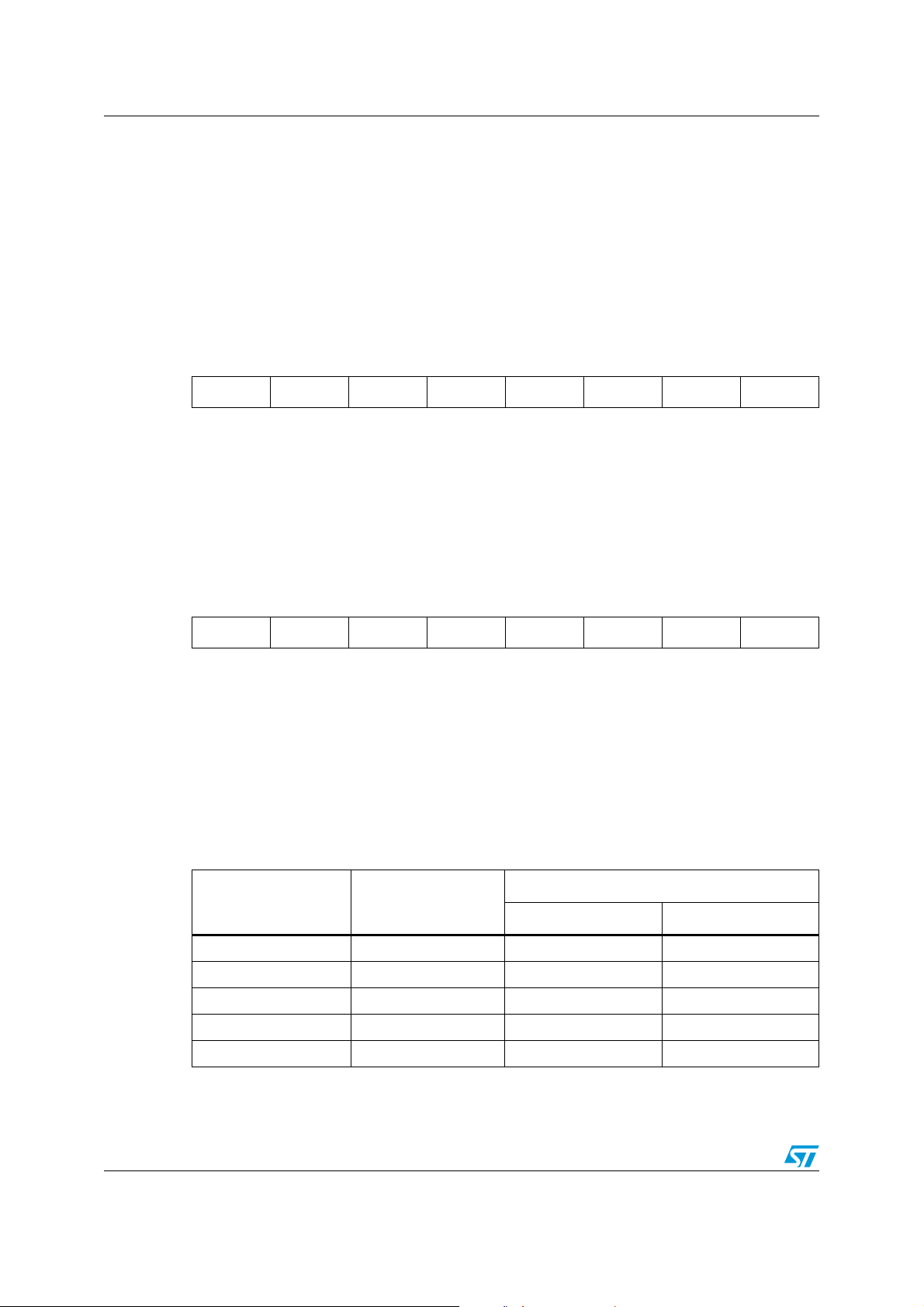
PWM auto-reload timer (ART) ST72361xx-Auto
Bit 0 = OVF Overflow Flag
This bit is set by hardware and cleared by software reading the ARTCSR register. It
indicates the transition of the counter from FFh to the ARTARR value
.
0: New transition not yet reached
1: Transition reached
Counter Access Register (ARTCAR)
Read/Write
Reset value: 0000 0000 (00h)
7 0
CA7 CA6 CA5 CA4 CA3 CA2 CA1 CA0
Bit 7:0 = CA[7:0] Counter Access Data
These bits can be set and cleared either by hardware or by software. The ARTCAR register
is used to read or write the auto-reload counter “on the fly” (while it is counting).
Auto-Reload Register (ARTARR)
Read/Write
Reset value: 0000 0000 (00h)
7 0
AR7 AR6 AR5 AR4 AR3 AR2 AR1 AR0
Bit 7:0 = AR[7:0] Counter Auto-Reload Data
These bits are set and cleared by software. They are used to hold the auto-reload value
which is automatically loaded in the counter when an overflow occurs. At the same time, the
PWM output levels are changed according to the corresponding OPx bit in the PWMCR
register.
This register has two PWM management functions:
● Adjusting the PWM frequency
● Setting the PWM duty cycle resolution
Table 44. PWM frequency vs resolution
f
ARTARR value Resolution
Min Max
0 8-bit ~0.244 kHz 31.25 kHz
[0..127] > 7-bit ~0.244 kHz 62.5 kHz
[128..191] > 6-bit ~0.488 kHz 125 kHz
[192..223] > 5-bit ~0.977 kHz 250 kHz
PWM
[224..239] > 4-bit ~1.953 kHz 500 kHz
98/279 Doc ID 12468 Rev 3

ST72361xx-Auto PWM auto-reload timer (ART)
PWM control register (PWMCR)
Read/write
Reset value: 0000 0000 (00h)
7 0
OE3 OE2 OE1 OE0 OP3 OP2 OP1 OP0
Bit 7:4 = OE[3:0] PWM Output Enable
These bits are set and cleared by software. They enable or disable the PWM output
channels independently acting on the corresponding I/O pin.
0: PWM output disabled.
1: PWM output enabled.
Bit 3:0 = OP[3:0] PWM Output Polarity
These bits are set and cleared by software. They independently select the polarity of the
four PWM output signals.
Table 45. PWMx output level and polarity
PWMx output level
OPx
Counter <= OCRx Counter > OCRx
100
011
Note: When an OPx bit is modified, the PWMx output signal polarity is immediately
reversed.
Duty cycle registers (PWMDCRx)
Read/write
Reset value: 0000 0000 (00h)
7 0
DC7 DC6 DC5 DC4 DC3 DC2 DC1 DC0
Bit 7:0 = DC[7:0] Duty Cycle Data
These bits are set and cleared by software.
A PWMDCRx register is associated with the OCRx register of each PWM channel to
determine the second edge location of the PWM signal (the first edge location is common to
all channels and given by the ARTARR register). These PWMDCR registers allow the duty
cycle to be set independently for each PWM channel.
Input Capture control / status register (ARTICCSR)
Read/Write
Reset value: 0000 0000 (00h)
Doc ID 12468 Rev 3 99/279

PWM auto-reload timer (ART) ST72361xx-Auto
7 0
0 0 CS2 CS1 CIE2 CIE1 CF2 CF1
Bit 7:6 = Reserved, always read as 0.
Bit 5:4 = CS[2:1] Capture Sensitivity
These bits are set and cleared by software. They determine the trigger event polarity on the
corresponding input capture channel.
0: Falling edge triggers capture on channel x.
1: Rising edge triggers capture on channel x.
Bit 3:2 = CIE[2:1] Capture Interrupt Enable
These bits are set and cleared by software. They enable or disable the Input capture
channel interrupts independently.
0: Input capture channel x interrupt disabled.
1: Input capture channel x interrupt enabled.
Bit 1:0 = CF[2:1] Capture Flag
These bits are set by hardware and cleared by software reading the corresponding
ARTICRx register. Each CFx bit indicates that an input capture x has occurred.
0: No input capture on channel x.
1: An input capture has occurred on channel x.
Input Capture Registers (ARTICRx)
Read only
Reset value: 0000 0000 (00h)
7 0
IC7 IC6 IC5 IC4 IC3 IC2 IC1 IC0
Bit 7:0 = IC[7:0] Input Capture Data
These read only bits are set and cleared by hardware. An ARTICRx register contains the 8bit auto-reload counter value transferred by the input capture channel x event.
Table 46. PWM auto-reload timer register map and reset values
Address
(Hex.)
0031h
0032h
0033h
0034h
Register label 7 6 5 4 3 2 1 0
PWMDCR3
Reset value
PWMDCR2
Reset value
PWMDCR1
Reset value
PWMDCR0
Reset value
DC70DC60DC50DC40DC30DC20DC10DC0
DC70DC60DC50DC40DC30DC20DC10DC0
DC70DC60DC50DC40DC30DC20DC10DC0
DC70DC60DC50DC40DC30DC20DC10DC0
0
0
0
0
100/279 Doc ID 12468 Rev 3
 Loading...