

3 A, 1.5 MHz PWM step-down switching regulator
Features
■ 1.5 MHz fixed frequency PWM with current
control mode
■ 3 A output current capability
■ Typical efficiency: > 90%
■ 2 % DC output voltage tolerance
■ Two versions available: power good or inhibit
■ Integrated output over-voltage protection
■ Non switching quiescent current: (typ) 1.5 mA
over temperature range
■ R
■ Utilizes tiny capacitors and inductors
■ Operating junction temp. -25 °C to 125 °C
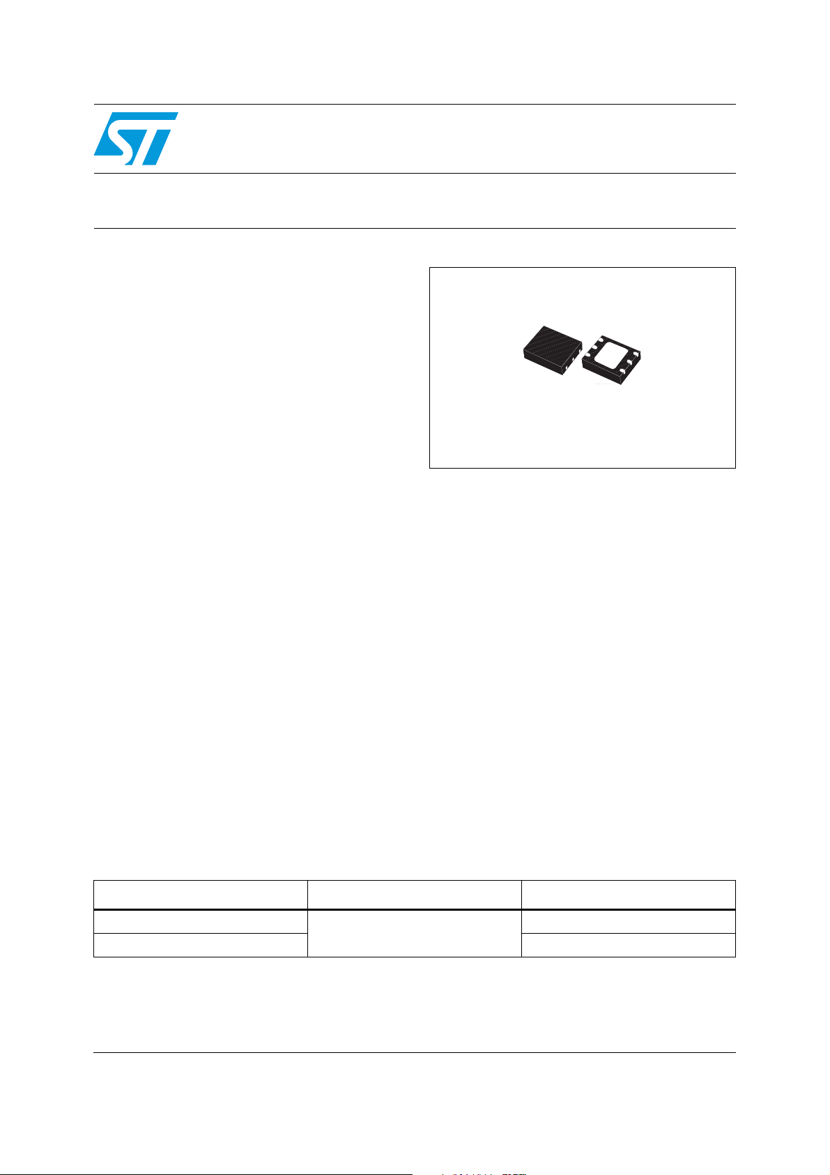
■ Available in DFN8 (4 x 4 mm) exposed pad
Description
The ST1S30 is a step-down DC-DC converter
optimized for powering low output voltage
applications. It supplies a current in excess of 3 A
over an input voltage range from 2.7 V to 6 V.
A high PWM switching frequency (1.5 MHz)
allows the use of tiny surface-mount components.
(typ) 100 mΩ
DSon
ST1S30
with synchronous rectification
DFN8 (4 x 4 mm)
Moreover, since the required synchronous
rectifier is integrated, the number of the external
components is reduced to minimum: a resistor
divider, an inductor and two capacitors. The
Power Good function continuously monitors the
output voltage. An open drain Power Good flag is
released when the output voltage is within
regulation. In addition, a low output ripple is
guaranteed by the current mode PWM topology
and by the use of low ESR SMD ceramic
capacitors. The device is thermally protected and
the output current limited to prevent damages due
to accidental short circuit. The ST1S30 is
available in the DFN8 (4 x 4 mm) package.
Table 1. Device summary
Order codes Package Note
ST1S30PUR
ST1S30IPUR INHIBIT version
1. Available on request.
September 2010 Doc ID 17927 Rev 1 1/11
(1)
DFN8 (4 x 4 mm)
PG version
www.st.com
11

Contents ST1S30
Contents
1 Diagram . . . . . . . . . . . . . . . . . . . . . . . . . . . . . . . . . . . . . . . . . . . . . . . . . . . 3
2 Pin configuration . . . . . . . . . . . . . . . . . . . . . . . . . . . . . . . . . . . . . . . . . . . . 4
3 Maximum ratings . . . . . . . . . . . . . . . . . . . . . . . . . . . . . . . . . . . . . . . . . . . . 5
4 Electrical characteristics . . . . . . . . . . . . . . . . . . . . . . . . . . . . . . . . . . . . . 6
5 Typical application circuits . . . . . . . . . . . . . . . . . . . . . . . . . . . . . . . . . . . 8
6 Package mechanical data . . . . . . . . . . . . . . . . . . . . . . . . . . . . . . . . . . . . . 9
7 Revision history . . . . . . . . . . . . . . . . . . . . . . . . . . . . . . . . . . . . . . . . . . . 10
2/11 Doc ID 17927 Rev 1
ST1S30 Diagram
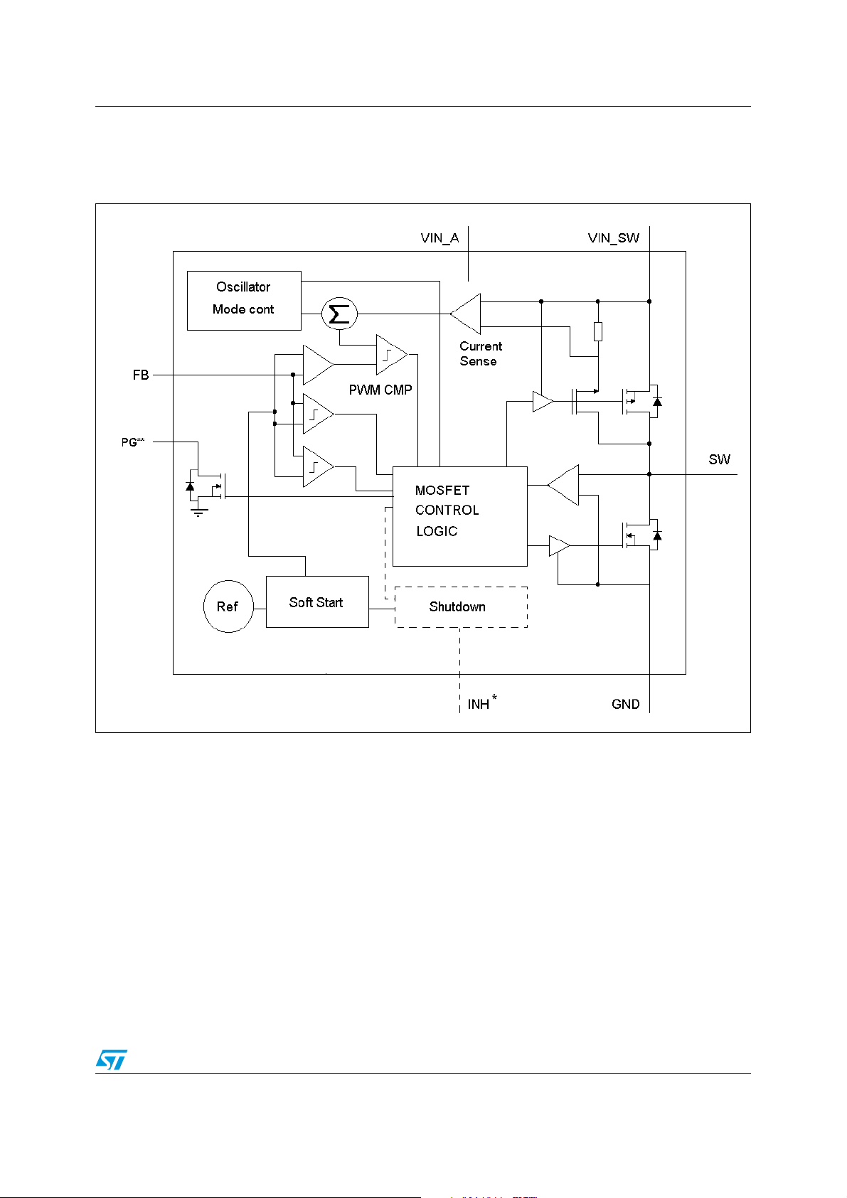
1 Diagram
Figure 1. Schematic diagram
(*) Only for ST1S30I
(**) Only for ST1S30
Doc ID 17927 Rev 1 3/11
Pin configuration ST1S30
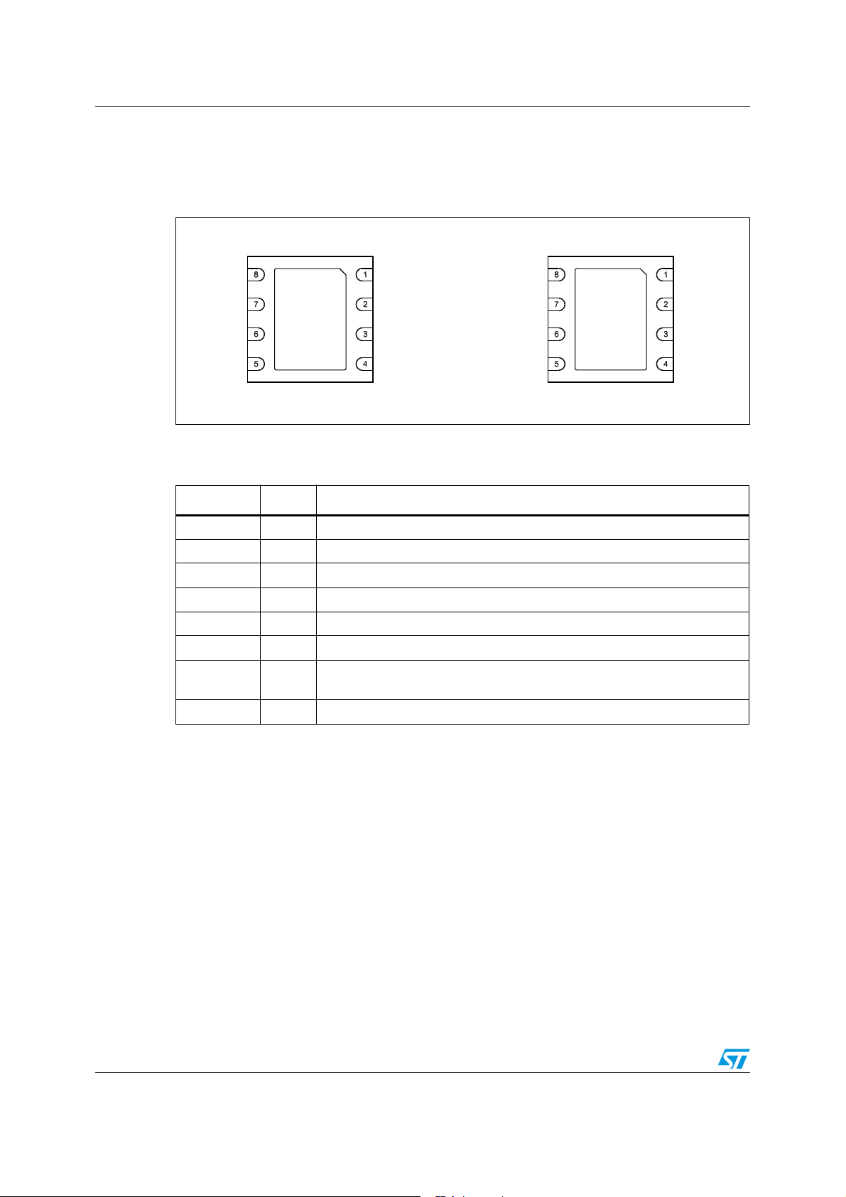
2 Pin configuration
Figure 2. Pin connections (top view)
ST1S30PUR
ST1S30IPUR
Table 2. Pin description
Pin n° Symbol Name and function
1 FB Feedback voltage
2 GND System ground
3 SW Switching pin
6V
IN_SW
7V
8 INH/PG Inhibit (INH) for ST1S30IPUR or Power Good (PG) for ST1S30PUR
Exposed pad GND
4, 5 NC Not internally connected. Can be connected to GND or left floating
Power supply for the MOSFET switch
Power supply for analog circuit
IN_A
To be connected to PCB ground plane for optimal electrical and thermal
performance
!-V
4/11 Doc ID 17927 Rev 1

ST1S30 Maximum ratings
3 Maximum ratings
Table 3. Absolute maximum ratings
Symbol Parameter Value Unit
V
IN_SW
V
V
IN_A
INH
Positive power supply voltage -0.3 to 7 V
Positive power supply voltage -0.3 to 7 V
Inhibit voltage (I version) -0.3 to VI + 0.3 V
SWITCH voltage Max. voltage of output pin -0.3 to 7 V
V
FB
Feedback voltage -0.3 to 3 V
PG Power Good open drain -0.3 to 7 V
T
T
T
J
STG
LEAD
Max junction temperature -40 to 150 °C
Storage temperature range -65 to 150 °C
Lead temperature (soldering) 10 sec 260 °C
Note: Absolute maximum ratings are those values beyond which damage to the device may occur.
Functional operation under these conditions is not implied.
Table 4. Thermal data
Symbol Parameter Value Unit
R
thJC
R
thJA
Thermal resistance junction-case 10 °C/W
Thermal resistance junction-ambient 40 °C/W
Table 5. ESD performance
Symbol Parameter Test conditions Value Unit
ESD ESD protection voltage HBM 2 kV
ESD ESD protection voltage MM 500 V
Doc ID 17927 Rev 1 5/11

Electrical characteristics ST1S30
4 Electrical characteristics
Refer to Figure 3 application circuit V
C
= 22 µF, L1 = 2.2 µH, TJ = -25 to 125 °C (unless otherwise specified. Typical values are
2
IN_SW
= V
= 5 V, VO = 1.2 V, C1 = 10 µF,
IN_A
referred to 25 °C)
Table 6. Electrical characteristics for ST1S30
Symbol Parameter Test conditions Min. Typ. Max. Unit
FB Feedback voltage 784 800 816 mV
I
FB
V
UV
OVP
I
OVP
I
Q
I
O
%VO/ΔVIOutput line regulation VI = 2.7 V to 5.5 V, IO = 100 mA
%VO/ΔIOOutput load regulation IO = 10 mA to 3 A
VFB pin bias current 600 nA
Input voltage IO = 10 mA to 3 A 2.7 5.5 V
I
Rising 2.3 V
V
Under voltage lock out
LO
threshold
Overvoltage protection
threshold
Overvoltage protection
hysteresis
I
Hysteresis 150 mV
V
rising 1.05 VO1.1 V
O
falling 5 %
V
O
O
Overvoltage clamping current VO = 1.2 V 300 mA
V
> 1.2 V, not switching 1.5 2.5
Quiescent current
Output current VI = 2.7 to 5.5 V
INH
< 0.0 V, T = - 30 °C to 85 °C 1
V
INH
(1)
(1)
3A
(1)
0.16
0.2 %
mA
%V
ΔV
V
/
O
I
PWMf
D
MAX
PWM switching frequency VFB = 0.65 V 1.2 1.5 1.8 MHz
S
Maximum duty cycle 80 87 %
Power good output threshold 0.92 V
PG
Power good output voltage low I
-N NMOS switch on resistance ISW = 750 mA 0.1 Ω
R
DSON
-P PMOS switch on resistance ISW = 750 mA 0.1 Ω
R
DSON
I
SWL
T
SHDN
T
ν
HYS
Switching current limitation
Efficiency
(1)
Thermal shutdown 150 °C
Thermal shutdown hysteresis 20 °C
%VO/ΔIOLoad transient response
%VO/ΔIOShort circuit removal response
1. Guaranteed by design, but not tested in production.
= 6 mA open drain output 0.4 V
SINK
(1)
IO = 10 mA to 100 mA, VO = 3.3 V 65
= 100 mA to 3 A, VO = 3.3 V 85
I
O
= 100 mA to 1 A, TA = 25 °C
I
O
= tF ≥ 200 ns
t
R
= 10 mA to IO = short,
I
O
TA = 25 °C
(1)
(1)
6/11 Doc ID 17927 Rev 1
O
3.7 4.4 5.1 A
%
-10 +10 %V
-10 +10 %V
V
O
O

ST1S30 Electrical characteristics
Refer to Figure 4 application circuit V
= 22, C3 = 1 µF, L1 = 2.2 µH, T
= -25 to 125 °C (unless otherwise specified. Typical values
J
IN_SW
= V
IN_A
= V
= 5 V, VO = 1.2 V, C1 = 10 µF, C2
INH
are referred to 25 °C)
Table 7. Electrical characteristics for ST1S30I
Symbol Parameter Test conditions Min. Typ. Max. Unit
FB Feedback voltage 784 800 816 mV
I
FB
V
OVP
I
Q
I
O
V
INH
I
INH
%VO/ΔVIOutput line regulation VI = 2.7 V to 5.5 V, IO = 100 mA
%VO/ΔIOOutput load regulation IO = 10 mA to 2 A
PWMfSPWM switching frequency VFB = 0.65 V 1.2 1.5 1.8 MHz
D
MAX
R
DSON
R
DSON
I
SWL
ν
T
SHDN
T
HYS
%VO/ΔIOLoad transient response
%VO/ΔIOShort circuit removal response
1. Guaranteed by design, but not tested in production.
VFB pin bias current 600 nA
Minimum input voltage IO = 10 mA to 2 A 2.7 V
I
Overvoltage protection
threshold
Overvoltage protection
hysteresis
Quiescent current
Output current VI = 2.7 to 5.5 V
Inhibit threshold
VO rising 1.05 VO1.1 V
V
falling 5 %
O
V
> 1.2 V, not switching 1.5 2.5 mA
INH
< 0.0 V, T = - 30 °C to 85 °C 1 µA
V
INH
Device ON, V
(1)
= 2.7 to 5.5 V 1.3
I
= 2.7 to 5 V 1.2
I
3A
O
Device OFF 0.4
Inhibit pin current 2µA
(1)
(1)
0.16
0.2 0.6
Maximum duty cycle 80 87 %
-N NMOS switch on resistance ISW = 750 mA 0.1 Ω
-P PMOS switch on resistance ISW = 750 mA 0.1 Ω
Switching current limitation
Efficiency
(1)
(1)
3.7 4.4 5.1 A
IO = 10 mA to 100 mA, VO = 3.3 V 65
= 100 mA to 3 A, VO = 3.3 V 85
I
O
Thermal shutdown 150 °C
Thermal shutdown hysteresis 20 °C
I
= 100 mA to 1 A, TA = 25 °C
O
tR = tF ≥ 200 ns
= 10 mA to IO = short,
I
O
= 25 °C
T
A
(1)
(1)
-10 +10 %V
-10 +10 %V
%V
ΔV
%V
ΔI
%
V
VDevice ON, V
/
O
I
/
O
O
O
O
Doc ID 17927 Rev 1 7/11

Typical application circuits ST1S30
5 Typical application circuits
Figure 3. Application circuit fot V
OUT
> 1.2 V
Figure 4. Application circuit for 0.8 V < V
OUT
< 1.2 V
Note: These typical application circuits are provided to help designing the external components.
However, we recommend to thoroughly validate any circuit solution in the real application
environment conditions.
8/11 Doc ID 17927 Rev 1

ST1S30 Package mechanical data
6 Package mechanical data
In order to meet environmental requirements, ST offers these devices in different grades of
ECOPACK
specifications, grade definitions and product status are available at: www.st.com.
ECOPACK
Table 8. DFN8 (4x4) mechanical data
®
packages, depending on their level of environmental compliance. ECOPACK®
®
is an ST trademark.
mm.
Dim.
Min. Typ. Max.
A 0.80 0.90 1.00
A1 0 0.02 0.05
A3 0.20
b 0.23 0.30 0.38
D 3.90 4.00 4.10
D2 2.82 3.00 3.23
E 3.90 4.00 4.10
E2 2.05 2.20 2.30
e 0.80
L 0.40 0.50 0.60
Figure 5. DFN8 (4x4) mechanical dimensions
"
Doc ID 17927 Rev 1 9/11

Revision history ST1S30
7 Revision history
Table 9. Document revision history
Date Revision Changes
09-Sep-2010 1 First release
10/11 Doc ID 17927 Rev 1

ST1S30
Please Read Carefully:
Information in this document is provided solely in connection with ST products. STMicroelectronics NV and its subsidiaries (“ST”) reserve the
right to make changes, corrections, modifications or improvements, to this document, and the products and services described herein at any
time, without notice.
All ST products are sold pursuant to ST’s terms and conditions of sale.
Purchasers are solely responsible for the choice, selection and use of the ST products and services described herein, and ST assumes no
liability whatsoever relating to the choice, selection or use of the ST products and services described herein.
No license, express or implied, by estoppel or otherwise, to any intellectual property rights is granted under this document. If any part of this
document refers to any third party products or services it shall not be deemed a license grant by ST for the use of such third party products
or services, or any intellectual property contained therein or considered as a warranty covering the use in any manner whatsoever of such
third party products or services or any intellectual property contained therein.
UNLESS OTHERWISE SET FORTH IN ST’S TERMS AND CONDITIONS OF SALE ST DISCLAIMS ANY EXPRESS OR IMPLIED
WARRANTY WITH RESPECT TO THE USE AND/OR SALE OF ST PRODUCTS INCLUDING WITHOUT LIMITATION IMPLIED
WARRANTIES OF MERCHANTABILITY, FITNESS FOR A PARTICULAR PURPOSE (AND THEIR EQUIVALENTS UNDER THE LAWS
OF ANY JURISDICTION), OR INFRINGEMENT OF ANY PATENT, COPYRIGHT OR OTHER INTELLECTUAL PROPERTY RIGHT.
UNLESS EXPRESSLY APPROVED IN WRITING BY AN AUTHORIZED ST REPRESENTATIVE, ST PRODUCTS ARE NOT
RECOMMENDED, AUTHORIZED OR WARRANTED FOR USE IN MILITARY, AIR CRAFT, SPACE, LIFE SAVING, OR LIFE SUSTAINING
APPLICATIONS, NOR IN PRODUCTS OR SYSTEMS WHERE FAILURE OR MALFUNCTION MAY RESULT IN PERSONAL INJURY,
DEATH, OR SEVERE PROPERTY OR ENVIRONMENTAL DAMAGE. ST PRODUCTS WHICH ARE NOT SPECIFIED AS "AUTOMOTIVE
GRADE" MAY ONLY BE USED IN AUTOMOTIVE APPLICATIONS AT USER’S OWN RISK.
Resale of ST products with provisions different from the statements and/or technical features set forth in this document shall immediately void
any warranty granted by ST for the ST product or service described herein and shall not create or extend in any manner whatsoever, any
liability of ST.
ST and the ST logo are trademarks or registered trademarks of ST in various countries.
Information in this document supersedes and replaces all information previously supplied.
The ST logo is a registered trademark of STMicroelectronics. All other names are the property of their respective owners.
© 2010 STMicroelectronics - All rights reserved
STMicroelectronics group of companies
Australia - Belgium - Brazil - Canada - China - Czech Republic - Finland - France - Germany - Hong Kong - India - Israel - Italy - Japan -
Malaysia - Malta - Morocco - Philippines - Singapore - Spain - Sweden - Switzerland - United Kingdom - United States of America
www.st.com
Doc ID 17927 Rev 1 11/11
 Loading...