查询ST1S03PM供应商
ST1S03
1.5A, 1.5 MHZ ADJUSTABLE,
STEP-DOWN SWITCHING REGULATOR IN DFN6
■ STEP-DOWN CURRENT MODE PWM
(1.5MHz) DC-DC CONVERTER
■ 2% DC OUTPUT VOLTAGE TOLERANCE
■ INTERNAL SOFT START FOR START-UP
CURRENT LIMITIATION AND POWER ON
DELAY OF 50-100µs
■ TYPICAL EFFICIENCY: > 70% OVER ALL
OPERATING C ON DITIONS
■ 1.5A OUTPUT CURRENT CAPAB ILITY
■ NOT SWITCHING QUIESCENT CURRENT:
MAX 2.5mA OVER TEMPERATURE RANGE
■ SWITCH V
■ USES TINY CAPACITO RS AND INDUCTORS
■ AVAILABLE IN DFN 3x3 EXPOSED PAD
: MAX 350mV @ISW=750mA
DS
DESCRIPTION
The ST1S03 is a step down DC-DC converter
optimized for powering low-voltage digital core in
HDD applications and, generally, to replace the
high current linear solution when the power
dissipation may cause an high heating of the
application environment. It provides up to 1.5A
over an input voltag e range o f 3V t o 16 V. A n hi gh
DFN6 (3x3)
switching frequency (1.5MHz) allows the use of
tiny surface-mount components: as well as the
resistor divider to set the output voltage value,
only an inductor, a schottky diode and two
capacitors are required. Besides, a low output
ripple is guaranteed by the current mode PWM
topology and by the use of low E.S.R. SMD
ceramic capacitors. The device is thermal
protected and current limited to prevent damages
due to accidental short circuit. The ST1S03 is
available in DFN6 package.
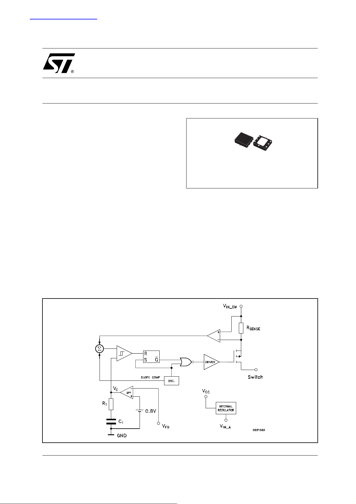
Figure 1: Schematic Diagram
Rev. 3
1/11March 2005
ST1S03
Table 1: Order Codes
SYMBOL DFN6 (Tape & Reel)
ST1S03 ST1S03PM ST1S03RPM
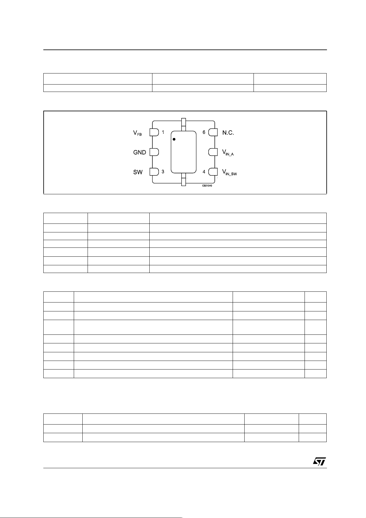
Figure 2: Pin Connec tion (top through view)
Table 2: Pin Description
PIN N° Symbol Name and Function
1
V
FB
2 GND Sistem Ground
3 SW Output of the internal Power Swithch
4
5
V
IN_SW
V
IN_A
6 N.C. Not Connected
Voltage of Feedback
Power Supply for the MOSFET Switch
Power Supply for the Analog Circuit
Table 3: Absolute Maximum Ratings
Symbol Parameter Value Unit
V
I_SW
V
I_SW
SWITCH
Voltage
V
I
VFB
T
T
STG
T
LEAD
Absolute Maximum Rat i ngs are thos e beyond which damage to the device may occ ur. Functional operati on under these condition is not implied.
Positive Power Supply Voltage
Positive Power Supply Voltage
Max Voltage of output pin
Feedback Voltage
FB
Common mode input voltage
Max Junction Temperature
J
Storage Temperature Range
Lead Temperature (Soldering) 10 Sec.
-0.3 to 16 V
-0.3 to 16 V
-0.3 to 16 V
2.5 V
±1 mA
150 °C
-25 to 150 °C
300 °C
Table 4: Thermal Data
Symbol Parameter DFN6 Unit
R
R
THJ-C
THJ-A
Thermal Resistance Junction-case
Thermal Resistance Junction-ambient
10 °C/W
55 °C/W
2/11
ST1S03
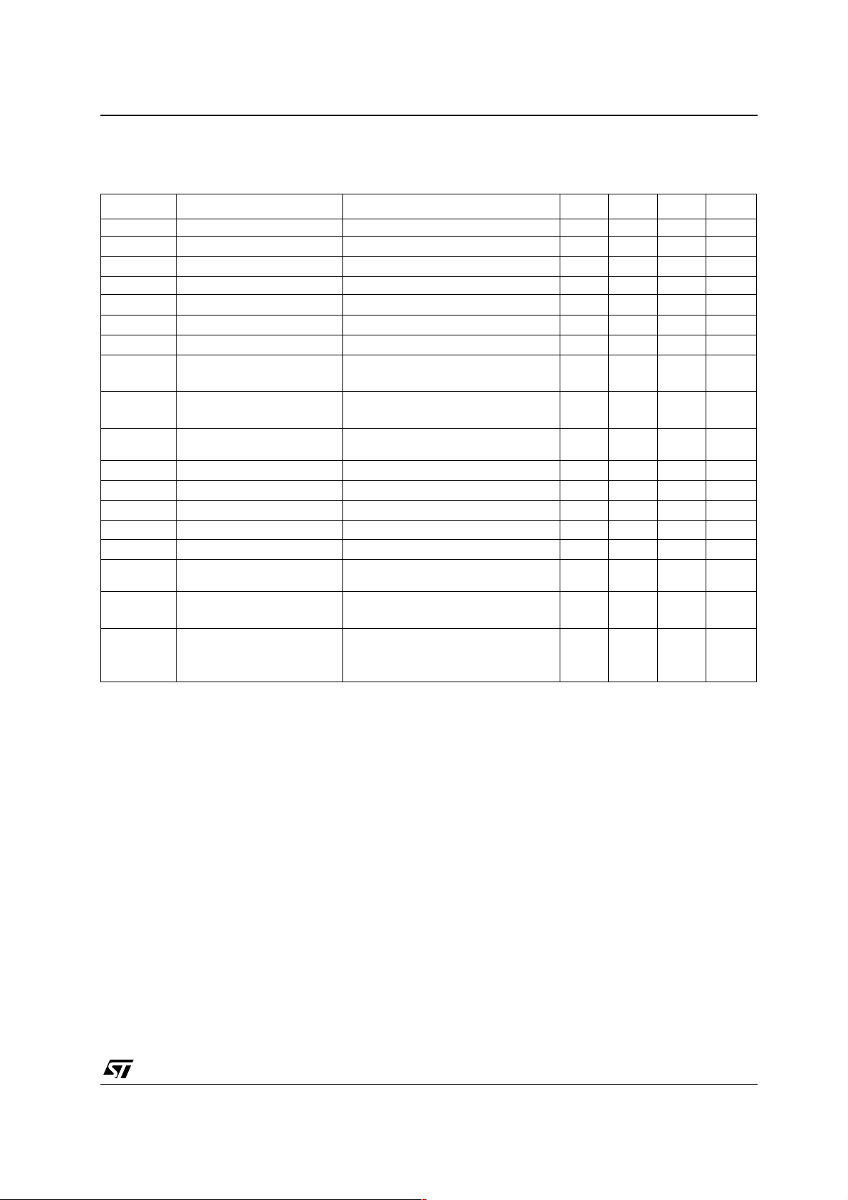
Table 5: Electrical Characteristics (V
IN_SW
= V
= 5V, CI = 4.7µF , CO = 22µF, L1 = 3.3µH, TJ = 0 to
IN_A
125°C, unless otherwise specified. Typical values are referred to 25°C)
Symbol Parameter Test Conditions Min. Typ. Max. Unit
FB Feedback Voltage 784 800 816 mV
PSRR Feedback PSRR 1Hz < Frequency V
I
FB
VFB Pin Bias Current 600 nA
IN
BW Bandwidth of Error Amplifier Closed Loop 300 KHz
I
Q
I
OUT
I
MIN
%V
OUT
∆V
%V
OUT
∆I
OUT
PWM f
D
MAX
I
SWL
V
DS
E Efficiency I
T
SHDN
T
HYS
∆V
OUT
∆I
OUT
∆V
OUT
∆I
OUT
Quiescent Current No Switching 2.5 mA
Output Current VIN =3V to 16V 1.5 A
Minimum Output Current 1 mA
/
Reference Line Regulation VIN = 3V to 16V 0.032 0.06 %V
IN
/
Reference Load Regulation I
PWM Switching Frequency
S
(1)
= 10mA to 1.2A 0.0014 0.003 %V
OUT
V
= 0.8V, TA =25°C 1.2 1.5 1.8 MHz
FB
Maximum Duty Cycle 87 %
Switching Current Limitation 1.65 A
Switch V
DS
ISW = 750 mA 200 350 mV
=10mA to 1.2A 70 %
OUT
Thermal Shut Down (1) 130 150 °C
Thermal Shut Down
Hysteresis (1)
/
Load Transient Response
(1)
Short Circuit Removal
/
Response (1)
I
= 100mA to 700mA
OUT
t
= tF ≥ 100ns, TA = 25°C
R
I
= 10mA to short, TA = 25°C +5 %V
OUT
-5 +5 %V
@IO = short
-60 dB
15 °C
/∆V
/mA
OUT
IN
OUT
O
O
NOTE 1: Guaranteed by design, not tes t ed i n production.
3/11
ST1S03
APPLICATION NOTES
The ST1S03 is an ad justable current m ode PWM
step-down DC/DC converter with internal 1.5A
power switch, packaged in a 6-lead DFN 3x3.
It’s a complete 1.5A switching regulator with its
internal compensation eliminating additional
component.
The constant frequency, current mode, PWM
architecture and stable operation with ceramic
capacitors results in low, predictable output ripple.
However, in order to keep the output regulated,
the devices goe s in pulse skipping m ode when a
very light load is required.
To clamp the error amplifier reference vol tage a
Soft Start control block generating a voltage ramp,
has been implemented. Besides an On-Chip
Power on Reset of 50 = 100µ s en sure the proper
operation when switching on the power supply.
Other circuits fitted to the device protection are the
Thermal Shut down block which turn off the
regulator when the junction tem perature exceeds
150°C typically and the Cycle-by-cycle Current
Limiting that provides protection against shorted
outputs.
Being the ST1S03 an adjustable regulator, the
output voltage is determined by an external
resistor divider. The desired valu e is given by t he
following equation:
V
= V
OUT
[1+R1/R2]
FB
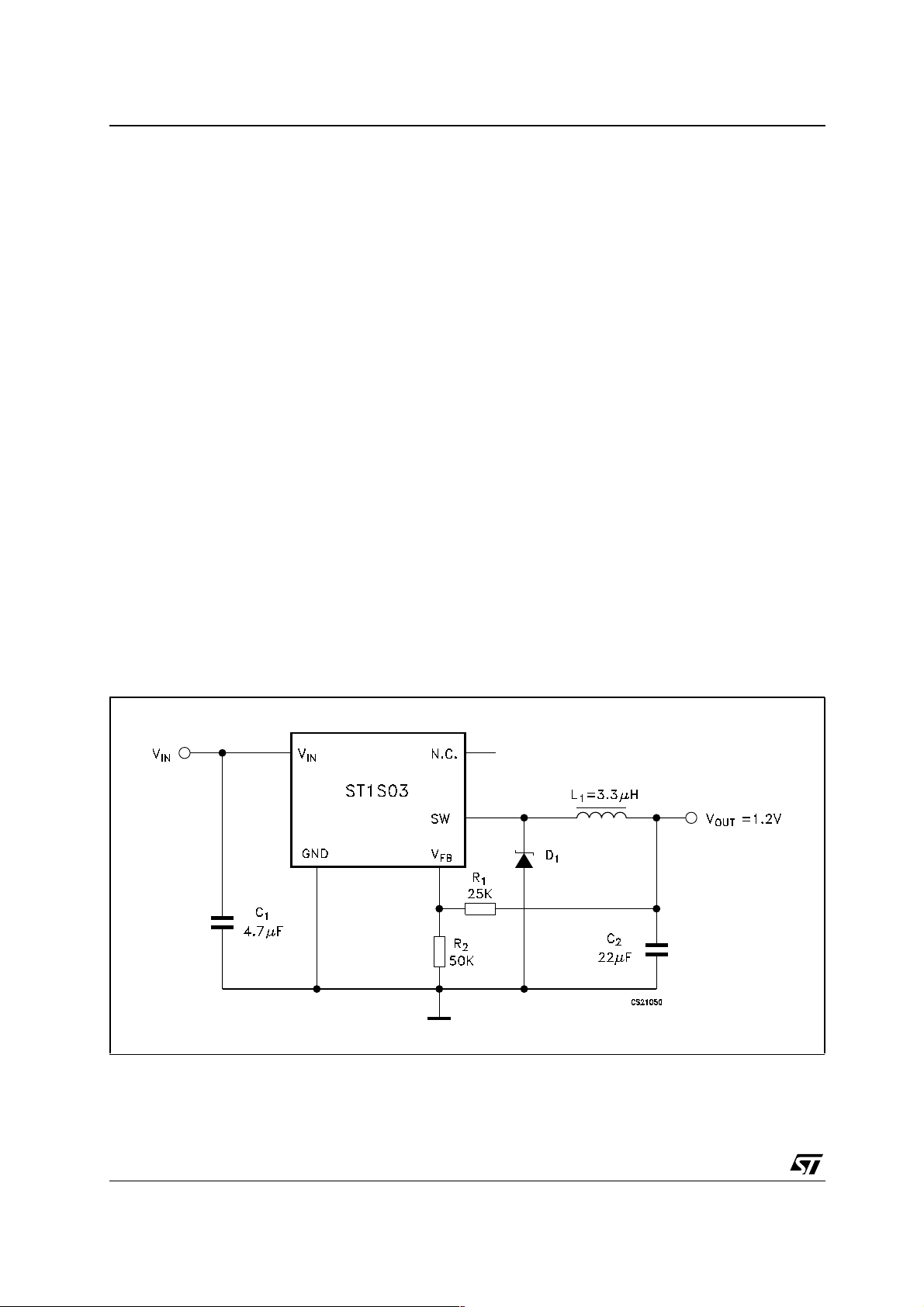
To make the device working, only other four
external components are required: a Schottky
diode, an inductor and two capacitors. The chosen
inductor must be able to not saturat e at the peak
current level. Besides, its value can be selected
keeping in account that a large inductor value
increases the efficiency at low ou tput current a nd
reduces output voltage ripple, while a smaller
inductor can be chosen when it is important to
reduce the pac kage s ize and the total cost of t he
application. Finally, the ST1S03 has been
designed to work p roperly with X5R or X7R SMD
ceramic capacitors both at the input and at the
output. this kind of capacitors, thanks to their very
low series resistance (ESR), minimize the output
voltage ripple. Other low ESR capacitors can be
used according to the need of the application
without invalidating the right functioning of the
device. Due to the high switching fr equency and
peak current, it is important to optimize the
application environment reducing the length of the
PCB traces and placing all the external
component near the device.
Figure 3: Applica tion Circuit
4/11
ST1S03
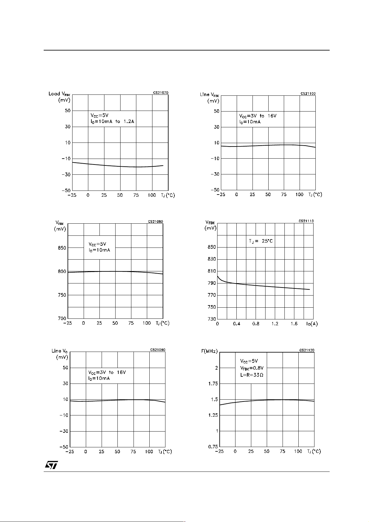
TYPICAL CHARACTERISTICS (CIN = 4.7µF, CO = 22µF, L1 = 3.3µH, unless otherwise specified)
Figure 4: Load Voltage Feedbac k vs
Temperature
Figure 5: Voltage Feedback vs Temperature
Figure 7: Line Voltage Feedback vs Temperature
Figure 8: Voltage Feedbac k vs Outp ut Current
Figure 6: Line Output Voltage Regulation vs
Temperature
Figure 9: PWM Switching Frequency vs
Temperature
5/11
ST1S03
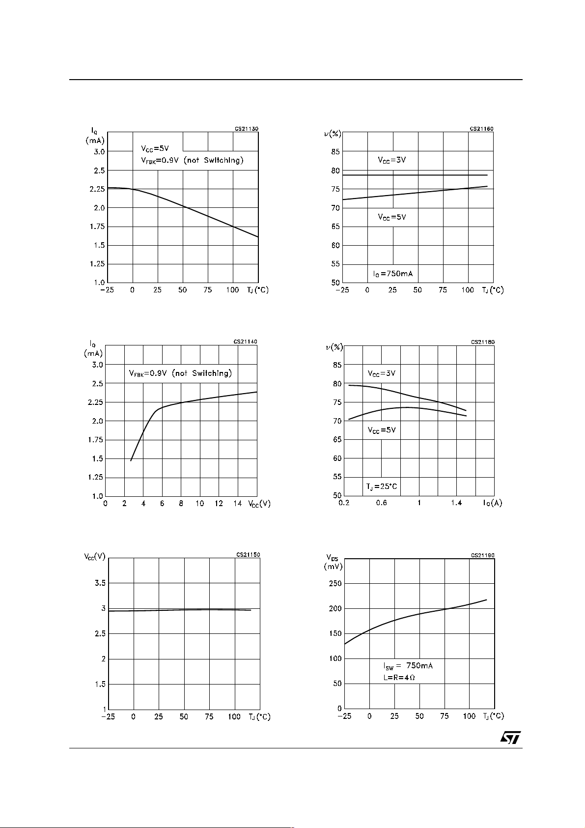
Figure 10: Quiescent Current vs Temperature
Figure 11: Quiescent Current vs Input Voltage
Figure 13: Efficiency vs Temperature
Figure 14: Efficiency vs Output Current
Figure 12: Minimum Operating Voltage vs Output
Voltage
6/11
Figure 15: Switch VDS vs Temperature
ST1S03
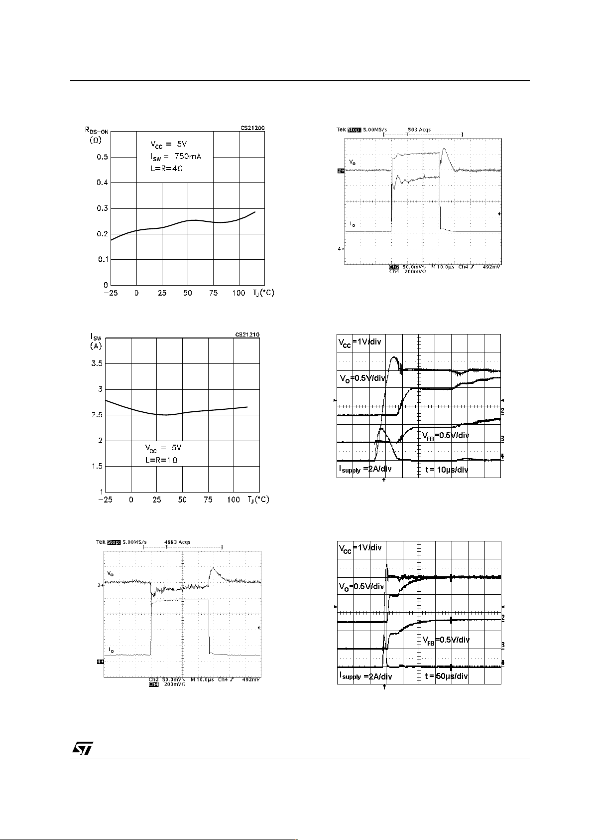
Figure 16: Switch RDS-ON vs Temperature
Figure 17: Switch Current Limitation vs
Temperature
Figure 19: Load Transient Response
VCC=5V, IO=200mA to 1.2A, CI=4.7µF, CO=22µF, L=3.3µH,
T
=38µs, TJ=25°C
ON
Figure 20: Start-Up Transient
Figure 18: Load Transient Response
VCC=5V, IO=100mA to 780mA, CI=4.7µF, CO=22µF, L=3.3µH,
=38µs, TJ=25°C
T
ON
VCC = 5V, TJ = 25°C
Figure 21: Start-Up Transient
VCC = 5V, TJ = 25°C
7/11

ST1S03
DFN6 (3x3) MECHANICAL DATA
mm. inch
DIM.
MIN. TYP MAX. MIN. TYP. MAX.
A 0.80 1.00 31.5 39.4
A1 0 0.05 0.0 2.0
A2 0.65 0.75 25.6 29.5
A3 0.20 7.9
b 0.33 0.43 13.0 16.9
D 2.90 3.00 3.10 114.2 118.1 122.0
D2 1.92 2.12 75.6 83.5
E 2.90 3.00 3.10 114.2 118.1 122.0
E2 1.11 1.31 43.7 51.6
e0.95 37.4
L 0.20 0.45 7.9 17.7
L1 0.24 9.4
L2 0.13 5.1
K 0.20 7.9
8/11
7387339A
ST1S03
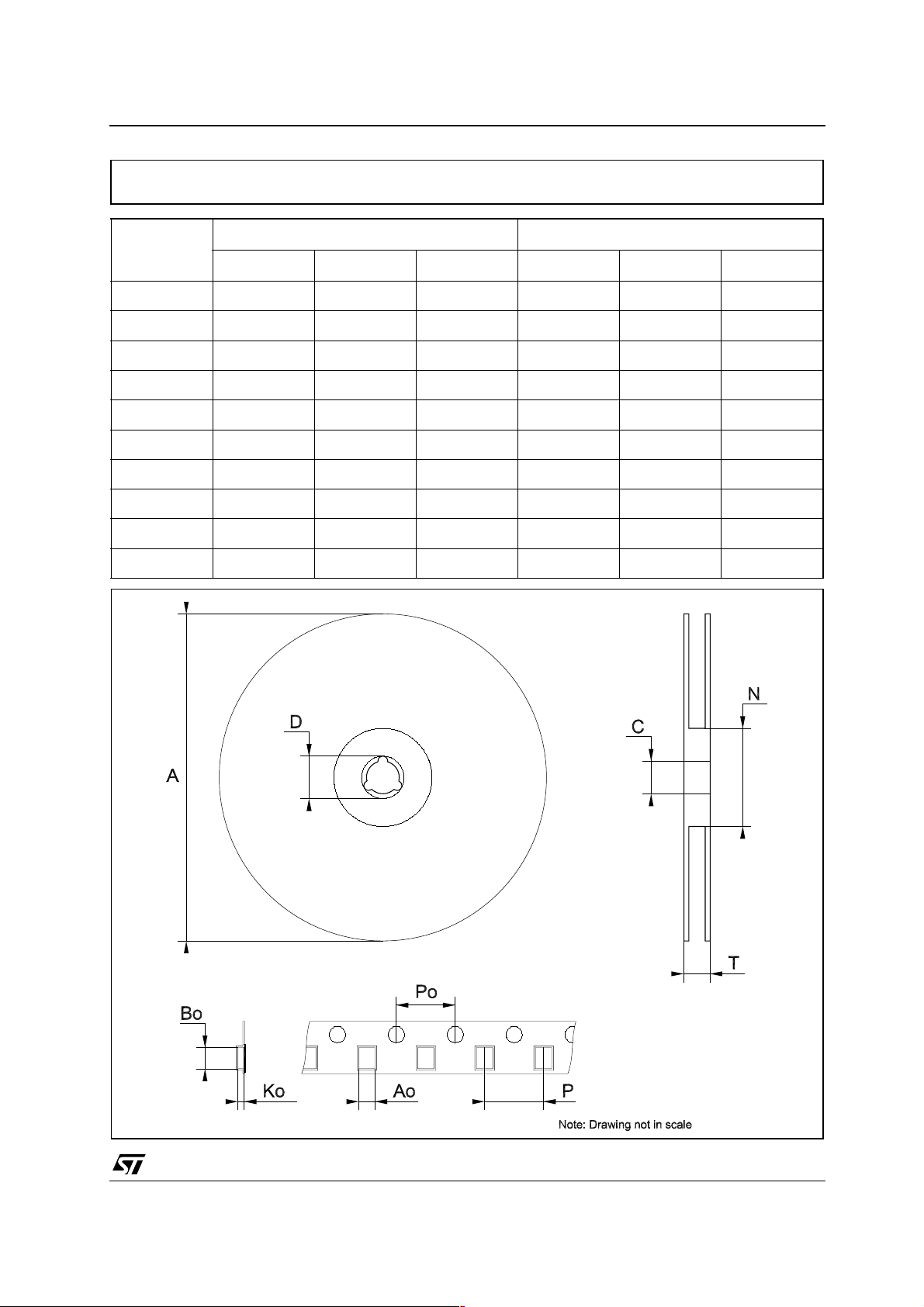
Tape & Reel QFNxx/DFNxx (3x3) MECHANICAL DATA
mm. inch
DIM.
MIN. TYP MAX. MIN. TYP. MAX.
A 330 12.992
C 12.8 13.2 0.504 0.519
D 20.2 0.795
N 99 101 3.898 3.976
T 14.4 0.567
Ao 3.3 0.130
Bo 3.3 0.130
Ko 1.1 0.043
Po 4 0.157
P 8 0.315
9/11

ST1S03
Table 6: Revision History
Date Revision Description of Change s
11-Nov-2004 1 First Release.
08-Feb-2005 2 Maturity Change.
03-Mar-2005 3
Mistake on Figure 1, T
is changed 125 ==> 150°C on Table 3.
J
10/11

ST1S03
Information furnished is believed to be accurate an d reliable. However, STMicroelectronics assumes no responsibility for the consequences
of use of such information nor for any infringement of patents or other rights of third parties which may result from its use. No license is granted
by implic ati o n or ot h er wis e und er an y pat ent or pa te nt r igh ts of STMi cr oe l ect ro ni cs . Sp ec if i cat i on s ment i o ned i n th is p ub li c ati on ar e s ubj ec t
to change without notice. This publication supersedes and replaces all information previously supplied. STMicroel ectronics products are not
authorized for use as critical components in life support devices or systems without express written approval of STMicroelectronics.
The ST logo is a registered trademark of STMicroelectronics
All other names are the property of their respective owners
© 2005 STMicroelectronics - All Rights Reserved
STMicroelectronics group of companies
Australia - Belgium - Brazil - Canada - China - Czech Republic - Finland - France - Germany - Hong Kong - India - Israel - Italy - Japan -
Malaysia - Malta - Morocco - Singapore - Spain - Sweden - Switzerland - United Kingdom - United States of America
www.st.com
11/11
 Loading...