

MEMS audio sensor omnidirectional digital microphone
Features
■ Single supply voltage
■ Low power consumption
■ 120 dBSPL acoustic overload point
■ 63 dB signal-to-noise ratio
■ Omnidirectional sensitivity
■ –26 dBFS sensitivity
■ PDM output
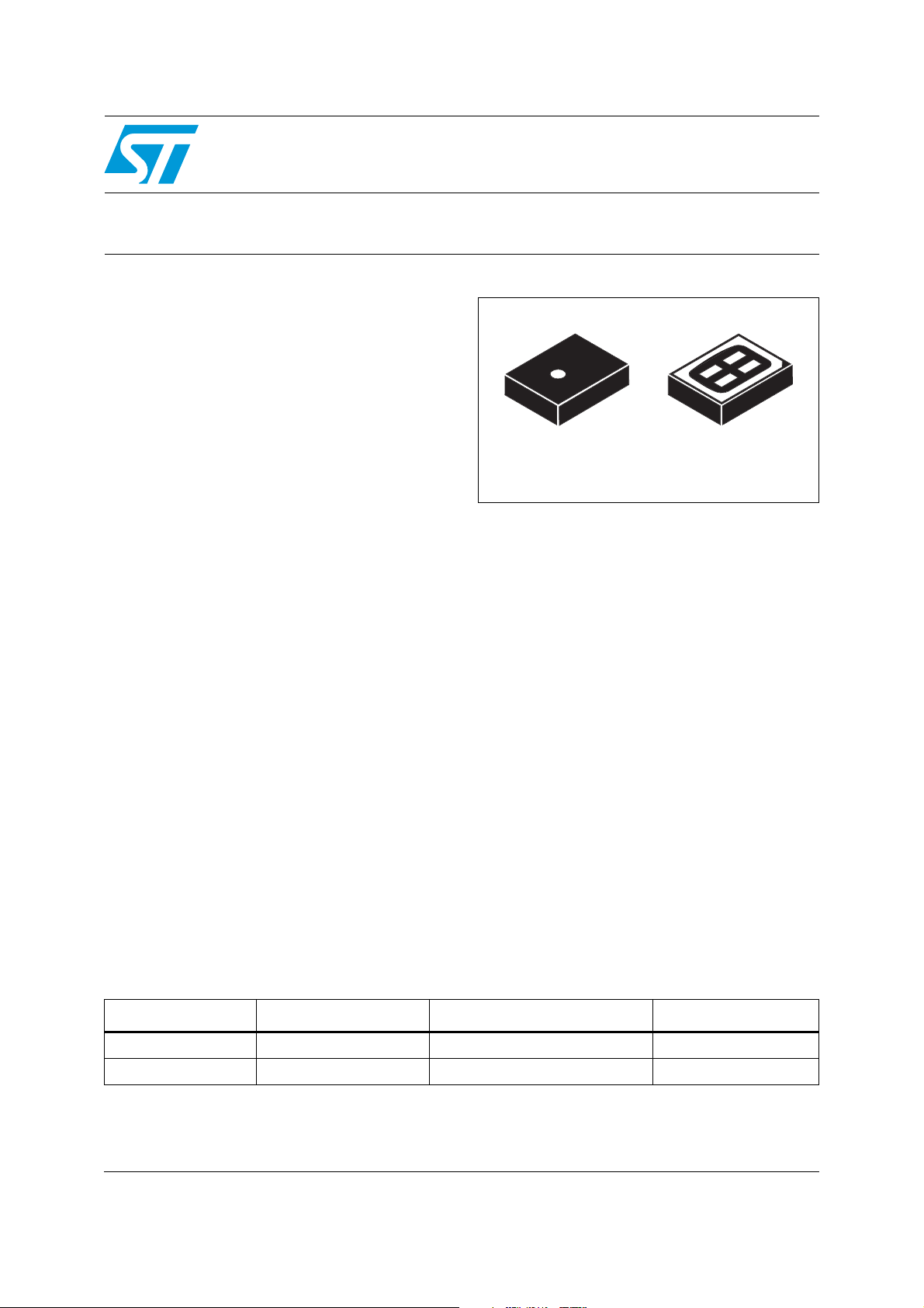
■ HCLGA package
– Top-port design
– SMD-compliant
– EMI-shielded
–ECOPACK
Applications
■ Mobile terminals
■ Laptop and notebook computers
■ Portable media players
■ VoIP
■ Speech recognition
■ A/V eLearning devices
■ Gaming and virtual reality input devices
■ Digital still and video cameras
■ Antitheft systems
Table 1. Device summary
®,
RoHS, and “Green” compliant
MP34DT01
Datasheet − production data
HCLGA 3x4x1 4LD
Description
The MP34DT01 is an ultra-compact, low-power,
omnidirectional, digital MEMS microphone built
with a capacitive sensing element and an IC
interface.
The sensing element, capable of detecting
acoustic waves, is manufactured using a
specialized silicon micromachining process
dedicated to produce audio sensors.
The IC interface is manufactured using a CMOS
process that allows designing a dedicated circuit
able to provide a digital signal externally in PDM
format.
The MP34DT01 has an acoustic overload point of
120 dBSPL with a 63 dB signal-to-noise ratio and
–26 dBFS sensitivity.
The MP34DT01 is available in a top-port, SMDcompliant, EMI-shielded package and is
guaranteed to operate over an extended
temperature range from -40 °C to +85 °C.
Part number Temperature range [°C] Package Packing
MP34DT01 -40 to +85 HCLGA (3 x 4 x 1) mm 4LD Tray
MP34DT01TR -40 to +85 HCLGA (3 x 4 x 1) mm 4LD Tape and reel
July 2012 Doc ID 022331 Rev 9 1/16
This is information on a product in full production.
www.st.com
1

Contents MP34DT01
Contents
1 Pin description . . . . . . . . . . . . . . . . . . . . . . . . . . . . . . . . . . . . . . . . . . . . . 5
2 Acoustic and electrical specifications . . . . . . . . . . . . . . . . . . . . . . . . . . 6
2.1 Acoustic and electrical characteristics . . . . . . . . . . . . . . . . . . . . . . . . . . . . 6
2.2 Timing characteristics . . . . . . . . . . . . . . . . . . . . . . . . . . . . . . . . . . . . . . . . 7
2.3 Frequency response . . . . . . . . . . . . . . . . . . . . . . . . . . . . . . . . . . . . . . . . . . 8
3 Sensing element . . . . . . . . . . . . . . . . . . . . . . . . . . . . . . . . . . . . . . . . . . . . 9
4 Absolute maximum ratings . . . . . . . . . . . . . . . . . . . . . . . . . . . . . . . . . . 10
5 Functionality . . . . . . . . . . . . . . . . . . . . . . . . . . . . . . . . . . . . . . . . . . . . . . 11
5.1 L/R channel selection . . . . . . . . . . . . . . . . . . . . . . . . . . . . . . . . . . . . . . . . 11
6 Package mechanical data . . . . . . . . . . . . . . . . . . . . . . . . . . . . . . . . . . . . 12
7 Revision history . . . . . . . . . . . . . . . . . . . . . . . . . . . . . . . . . . . . . . . . . . . 15
2/16 Doc ID 022331 Rev 9

MP34DT01 List of tables
List of tables
Table 1. Device summary . . . . . . . . . . . . . . . . . . . . . . . . . . . . . . . . . . . . . . . . . . . . . . . . . . . . . . . . . . 1
Table 2. Pin description . . . . . . . . . . . . . . . . . . . . . . . . . . . . . . . . . . . . . . . . . . . . . . . . . . . . . . . . . . . 5
Table 3. Acoustic and electrical characteristics . . . . . . . . . . . . . . . . . . . . . . . . . . . . . . . . . . . . . . . . . 6
Table 4. Distortion specifications . . . . . . . . . . . . . . . . . . . . . . . . . . . . . . . . . . . . . . . . . . . . . . . . . . . . 6
Table 5. Timing characteristics . . . . . . . . . . . . . . . . . . . . . . . . . . . . . . . . . . . . . . . . . . . . . . . . . . . . . . 7
Table 6. Frequency response mask for digital microphones . . . . . . . . . . . . . . . . . . . . . . . . . . . . . . . 8
Table 7. Absolute maximum ratings . . . . . . . . . . . . . . . . . . . . . . . . . . . . . . . . . . . . . . . . . . . . . . . . . 10
Table 8. L/R channel selection . . . . . . . . . . . . . . . . . . . . . . . . . . . . . . . . . . . . . . . . . . . . . . . . . . . . . 11
Table 9. Recommended soldering profile limits . . . . . . . . . . . . . . . . . . . . . . . . . . . . . . . . . . . . . . . . 12
Table 10. HCLGA 3 mm x 4 mm x 1 mm 4-lead package dimensions . . . . . . . . . . . . . . . . . . . . . . . . 13
Table 11. Document revision history . . . . . . . . . . . . . . . . . . . . . . . . . . . . . . . . . . . . . . . . . . . . . . . . . 15
Doc ID 022331 Rev 9 3/16

List of figures MP34DT01
List of figures
Figure 1. Pin connections . . . . . . . . . . . . . . . . . . . . . . . . . . . . . . . . . . . . . . . . . . . . . . . . . . . . . . . . . . 5
Figure 2. Timing waveforms. . . . . . . . . . . . . . . . . . . . . . . . . . . . . . . . . . . . . . . . . . . . . . . . . . . . . . . . . 7
Figure 3. Typical frequency response normalized at 1 kHz . . . . . . . . . . . . . . . . . . . . . . . . . . . . . . . . . 8
Figure 4. Recommended soldering profile limits . . . . . . . . . . . . . . . . . . . . . . . . . . . . . . . . . . . . . . . . 12
Figure 5. HCLGA 3 mm x 4 mm x 1 mm 4-lead package outline. . . . . . . . . . . . . . . . . . . . . . . . . . . . 13
Figure 6. Land pattern . . . . . . . . . . . . . . . . . . . . . . . . . . . . . . . . . . . . . . . . . . . . . . . . . . . . . . . . . . . . 14
4/16 Doc ID 022331 Rev 9

MP34DT01 Pin description
1 Pin description
Figure 1. Pin connections
(TOP VIEW)
Table 2. Pin description
Pin # Pin name Function
1 Vdd Power supply
2 LR Left/Right channel selection
3 CLK Synchronization input clock
4 DOUT Left/Right PDM data output
5 (ground ring) GND 0 V supply
LR
Vdd
2
3
1
4
GND
(BOTTOM VIEW)
CLK
DOUT
5
AM045273v1
Doc ID 022331 Rev 9 5/16

Acoustic and electrical specifications MP34DT01
2 Acoustic and electrical specifications
2.1 Acoustic and electrical characteristics
The values listed in the table below are specified for Vdd = 1.8 V, Clock = 2.4 MHz,
T = 25 °C, unless otherwise noted.
Table 3. Acoustic and electrical characteristics
Symbol Parameter Test condition Min. Typ.
Vdd Supply voltage 1.64 1.8 3.6 V
Idd
IddPdn
Current consumption in
normal mode
Current consumption in
power-down mode
(2)
Mean value 0.6 mA
Scc Short-circuit current 1 10 mA
AOP Acoustic overload point 120 dBSPL
So Sensitivity -29 -26 -23 dBFS
SNR Signal-to-noise ratio
A-weighted at 1 kHz,
1 Pa
PSR Power supply rejection Guaranteed by design -70 dBFS
Clock Input clock frequency
Ton Turn-on time
To p
V
V
1. Typical specifications are not guaranteed.
2. Input clock in static mode.
3. Duty cycle: min = 40% max = 60%.
4. Time from the first clock edge to valid output data.
Operating temperature
range
Low level logic
IOL
input/output voltage
High level logic
IOH
input/output voltage
(4)
(3)
1 2.4 3.25 MHz
Guaranteed by design 10 ms
-40 +85 °C
= 1 mA -0.3 0.35xVdd V
I
out
= 1 mA 0.65xVdd Vdd+0.3 V
I
out
(1)
Max. Unit
20 µA
63 dB
Table 4. Distortion specifications
Parameter Test condition Value
Distortion 100 dBSPL (50 Hz - 4 kHz) < 1% THD + N
Distortion 115 dBSPL (1 kHz) < 5% THD + N
6/16 Doc ID 022331 Rev 9

MP34DT01 Acoustic and electrical specifications
2.2 Timing characteristics
Table 5. Timing characteristics
Parameter Description Min Max Unit
f
CLK
f
PD
T
CLK
T
R,EN
T
R,DIS
T
L,EN
T
L,DIS
1. From design simulations
Clock frequency for normal mode 1 3.25 MHz
Clock frequency for power-down mode 0.23 MHz
Clock period for normal mode 308 1000 ns
Data enabled on DATA line, L/R pin = 1 18
Data disabled on DATA line, L/R pin = 1 16
Data enabled on DATA line, L/R pin = 0 18
Data disabled on DATA line, L/R pin = 0 16
Figure 2. Timing waveforms
CLK
T
R,EN
PDM R
T
R,DIS
High Z
(1)
(1)
(1)
(1)
T
CLK
T
L,DIS
High Z
ns
ns
ns
ns
PDM L
T
L,EN
High Z
High Z
AM045165v1
Doc ID 022331 Rev 9 7/16

Acoustic and electrical specifications MP34DT01
2.3 Frequency response
Figure 3. Typical frequency response normalized at 1 kHz
10
8
6
4
2
0
-2
Normalized Sensitivity [dB]
-4
-6
-8
-10
10 100 1000 10000
Frequency [Hz]
Table 6. Frequency response mask for digital microphones
Frequency / Hz
20...100 -5 +5 dBr 1kHz
100...8000 -2 +2 dBr 1kHz
8000...20000 -5 +5 dBr 1kHz
1. At T = 20 °C and acoustic stimulus = 1 Pa (94 dB SPL)
(1)
Lower limit Upper limit Unit
AM045317v1
8/16 Doc ID 022331 Rev 9

MP34DT01 Sensing element
3 Sensing element
The sensing element shall mean the acoustic sensor consisting of a conductive movable
plate and a fixed plate placed in a tiny silicon chip. This sensor transduces the sound
pressure into the changes of coupled capacity between those two plates.
Omron Corporation supplies this element for STMicroelectronics.
Doc ID 022331 Rev 9 9/16

Absolute maximum ratings MP34DT01
4 Absolute maximum ratings
Stresses above those listed as “absolute maximum ratings” may cause permanent damage
to the device. This is a stress rating only and functional operation of the device under these
conditions is not implied. Exposure to maximum rating conditions for extended periods may
affect device reliability.
Table 7. Absolute maximum ratings
Symbol Ratings Maximum value Unit
Vdd Supply voltage -0.3 to 6 V
Vin Input voltage on any control pin -0.3 to Vdd +0.3 V
T
ESD Electrostatic discharge protection 2 (HBM) kV
Storage temperature range -40 to +125 °C
STG
This device is sensitive to mechanical shock, improper handling can cause
permanent damage to the part.
This device is ESD-sensitive, improper handling can cause permanent damage to the
part.
10/16 Doc ID 022331 Rev 9

MP34DT01 Functionality
5 Functionality
5.1 L/R channel selection
The L/R digital pad lets the user select the DOUT signal pattern as shown in Tabl e 8 . The
L/R pin must be connected to Vdd or GND.
Table 8. L/R channel selection
L/R CLK low CLK high
GND Data valid High impedance
Vdd High impedance Data valid
Doc ID 022331 Rev 9 11/16

Package mechanical data MP34DT01
6 Package mechanical data
In order to meet environmental requirements, ST offers these devices in different grades of
ECOPACK
specifications, grade definitions and product status are available at: www.st.com.
ECOPACK
®
packages, depending on their level of environmental compliance. ECOPACK®
®
is an ST trademark.
Soldering information
The HCLGA 3x4 4LD package is also compliant with the RoHS and “Green” standards and
is qualified for soldering heat resistance according to JEDEC J-STD-020.
Landing pattern and soldering recommendations are available at www.st.com.
Figure 4. Recommended soldering profile limits
t
p
T
P
T
L
TEMPERATURE
RAMP-UP
T
SMAX
T
SMIN
t
s
PREHEAT
RAMP-DOWN
t
L
CRITICAL ZONE
TLto T
P
T25°C to PEAK
30 60 90 120 150 180 210 240 270 300 330 360 390
TIME
AM045166v1
Table 9. Recommended soldering profile limits
Description Parameter Pb free
Average ramp rate TL to T
P
Preheat
Minimum temperature
Maximum temperature
Time (T
SMIN
to T
SMAX
)
Ramp-up rate T
Time maintained above liquidous temperature
Liquidous temperature
Peak temperature T
T
SMIN
T
SMAX
SMAX
t
t
T
S
to T
L
L
P
L
Time within 5 °C of actual peak temperature 20 sec to 40 sec
Ramp-down rate 6 °C/sec max
Time 25 °C (t25 °C) to peak temperature 8 minutes max
3 °C/sec max
150 °C
200 °C
60 sec to 120 sec
60 sec to 150 sec
217 °C
260 °C max
12/16 Doc ID 022331 Rev 9

MP34DT01 Package mechanical data
Figure 5. HCLGA 3 mm x 4 mm x 1 mm 4-lead package outline
2
E1
K
E
D
1
D
1
R
E2
TOP VIEW
2
D
//
K C
K E
K D
C
K
1
G
1
N
Seating Plane
1
A
1
L
6
G
X
4
T
2
BOTTOM VIEW
L
N2
G5XG5 Pin 1 Indicator
1
1
4
2
3
T
1
T
M
T
2
3
G
2
G
G4
8053274_D
Table 10. HCLGA 3 mm x 4 mm x 1 mm 4-lead package dimensions
mm
Symbol
Min Typ Max
A1 0.900 1.000 1.100
D1 3.900 4.000 4.100
D2 0.300 0.500 0.700
R1 0.300 0.400 0.500
E1 2.900 3.000 3.100
E2 0.000 ±0.200
L1 1.300 1.350 1.400
L2 0.800 0.850 0.900
N1 0.625 0.675 0.725
N2 0.375 0.425 0.475
T1 0.900 0.950 1.000
T2 0.350 0.400 0.450
G1 3.050 3.100 3.150
G2 3.750 3.800 3.850
G3 2.050 2.100 2.150
G4 2.750 2.800 2.850
G5 0.250 0.300 0.350
G6 0.400
M0.100
K0.050
Doc ID 022331 Rev 9 13/16

Package mechanical data MP34DT01
Figure 6. Land pattern
0.85
GND
1.30
GND
CLK
DOUT
GND
0.35
0.40
LR
0.95
Vdd
Pad + solder paste
0.35
GND
0.85
2.30
14/16 Doc ID 022331 Rev 9

MP34DT01 Revision history
7 Revision history
Table 11. Document revision history
Date Revision Changes
06-Oct-2011 1 Initial release
18-Nov-2011 2 Removed “stereo” from title, Features, and Description
29-Nov-2011 3 Updated Features and Description
Updated Figure 3: Typical frequency response normalized at 1 kHz
04-Jan-2012 4
23-Mar-2012 5
Added So limits to Table 3: Acoustic and electrical characteristics
Minor textual updates
Updated Figure 5: HCLGA 3 mm x 4 mm x 1 mm 4-lead package outline
Pin 1 indicator removed from top view of package on page 1 and
Figure 1: Pin connections
Updated Table 10: HCLGA 3 mm x 4 mm x 1 mm 4-lead package
dimensions
06-Apr-2012 6
07-May-2012 7 Added V
Updated maximum supply voltage in Table 3: Acoustic and electrical
characteristics
, V
IOL
to Table 3: Acoustic and electrical characteristics
IOH
18-May-2012 8 Updated Table 5: Timing characteristics
Added Section 3: Sensing element
05-Jul-2012 9
Added Figure 6: Land pattern
Updated temperature range to -40 to +85 °C throughout datasheet
Doc ID 022331 Rev 9 15/16

MP34DT01
Please Read Carefully:
Information in this document is provided solely in connection with ST products. STMicroelectronics NV and its subsidiaries (“ST”) reserve the
right to make changes, corrections, modifications or improvements, to this document, and the products and services described herein at any
time, without notice.
All ST products are sold pursuant to ST’s terms and conditions of sale.
Purchasers are solely responsible for the choice, selection and use of the ST products and services described herein, and ST assumes no
liability whatsoever relating to the choice, selection or use of the ST products and services described herein.
No license, express or implied, by estoppel or otherwise, to any intellectual property rights is granted under this document. If any part of this
document refers to any third party products or services it shall not be deemed a license grant by ST for the use of such third party products
or services, or any intellectual property contained therein or considered as a warranty covering the use in any manner whatsoever of such
third party products or services or any intellectual property contained therein.
UNLESS OTHERWISE SET FORTH IN ST’S TERMS AND CONDITIONS OF SALE ST DISCLAIMS ANY EXPRESS OR IMPLIED
WARRANTY WITH RESPECT TO THE USE AND/OR SALE OF ST PRODUCTS INCLUDING WITHOUT LIMITATION IMPLIED
WARRANTIES OF MERCHANTABILITY, FITNESS FOR A PARTICULAR PURPOSE (AND THEIR EQUIVALENTS UNDER THE LAWS
OF ANY JURISDICTION), OR INFRINGEMENT OF ANY PATENT, COPYRIGHT OR OTHER INTELLECTUAL PROPERTY RIGHT.
UNLESS EXPRESSLY APPROVED IN WRITING BY TWO AUTHORIZED ST REPRESENTATIVES, ST PRODUCTS ARE NOT
RECOMMENDED, AUTHORIZED OR WARRANTED FOR USE IN MILITARY, AIR CRAFT, SPACE, LIFE SAVING, OR LIFE SUSTAINING
APPLICATIONS, NOR IN PRODUCTS OR SYSTEMS WHERE FAILURE OR MALFUNCTION MAY RESULT IN PERSONAL INJURY,
DEATH, OR SEVERE PROPERTY OR ENVIRONMENTAL DAMAGE. ST PRODUCTS WHICH ARE NOT SPECIFIED AS "AUTOMOTIVE
GRADE" MAY ONLY BE USED IN AUTOMOTIVE APPLICATIONS AT USER’S OWN RISK.
Resale of ST products with provisions different from the statements and/or technical features set forth in this document shall immediately void
any warranty granted by ST for the ST product or service described herein and shall not create or extend in any manner whatsoever, any
liability of ST.
ST and the ST logo are trademarks or registered trademarks of ST in various countries.
Information in this document supersedes and replaces all information previously supplied.
The ST logo is a registered trademark of STMicroelectronics. All other names are the property of their respective owners.
© 2012 STMicroelectronics - All rights reserved
STMicroelectronics group of companies
Australia - Belgium - Brazil - Canada - China - Czech Republic - Finland - France - Germany - Hong Kong - India - Israel - Italy - Japan -
Malaysia - Malta - Morocco - Philippines - Singapore - Spain - Sweden - Switzerland - United Kingdom - United States of America
www.st.com
16/16 Doc ID 022331 Rev 9
 Loading...