

Page 1
MP38115
Ultra Low Voltage, 4A, 5.5V Synchronous
The Future of Analog IC Technology
DESCRIPTION
The MP38115 is an internally compensated
1.5MHz fixed frequency PWM synchronous
step-down regulator. MP38115 operates from a
1.1V to 5.5V input and generates an output
voltage as low as 0.8V.
The MP38115 integrates a 60m high-side
switch and a 60m synchronous rectifier for
high efficiency without an external Schottky
diode. With peak current mode control and
internal compensation, the MP38115 based
solution delivers a very compact footprint with a
minimum component count.
The MP38115 is available in a small 3mm x
3mm 10-lead QFN package.
Step-Down Switching Regulator
FEATURES
• 4A Output Current
• Input Operation Range: 1.1V to 5.5V
• 60m Internal Power MOSFET Switches
• All Ceramic Capacitor Design
• Up to 95% Efficiency
• 1.5MHz Fixed Switching Frequency
• Adjustable Output from 0.8V to 0.9xV
IN
• Internal Soft-Start
• Frequency Synchronization Input
• Power Good Output
• Cycle-by-Cycle Current Limiting
• Hiccup Short Circuit Protection
• Thermal Shutdown
• 3mm x 3mm 10-lead QFN Package
APPLICATIONS
• µP/ASIC/DSP/FPGA Core and I/O Supplies
• Printers and LCD TVs
• Network and Telecom Equipment
• Point of Load Regulators
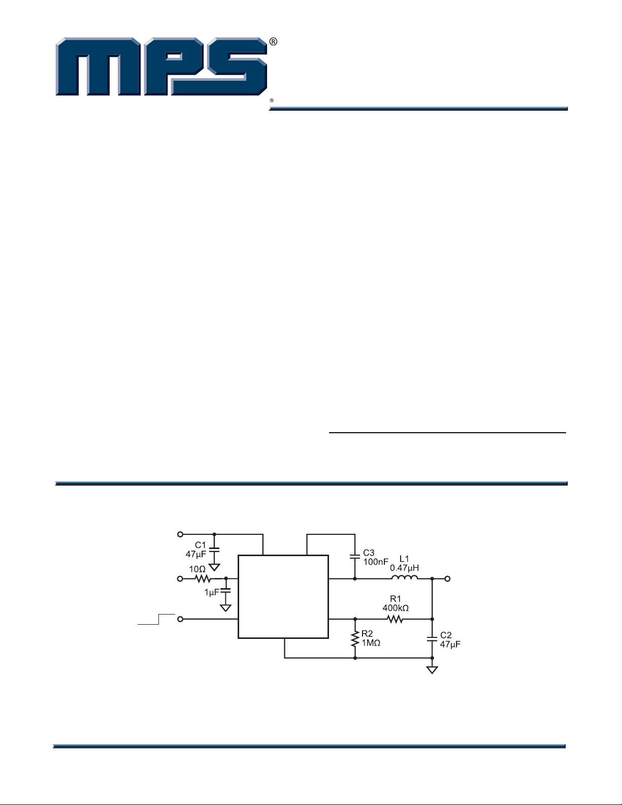
TYPICAL APPLICATION
V
1.1V to 5.5V
2.7V to 5.5V
IN
V
CC
OFF ON
VCC
MP38115
EN/SYNC
GND
“MPS” and “The Future of Analog IC Technology” are Registered Trademarks of
Monolithic Power Systems, Inc.
BSIN
SW
FB
V
OUT
1.1V / 4A
MP38115 Rev. 0.92 www.MonolithicPower.com 1
8/11/2009 MPS Proprietary Information. Unauthorized Photocopy and Duplication Prohibited.
© 2009 MPS. All Rights Reserved.
Page 2
MP38115 – 4A, 5.5V SYNCHRONOUS STEP-DOWN SWITCHING REGULATOR
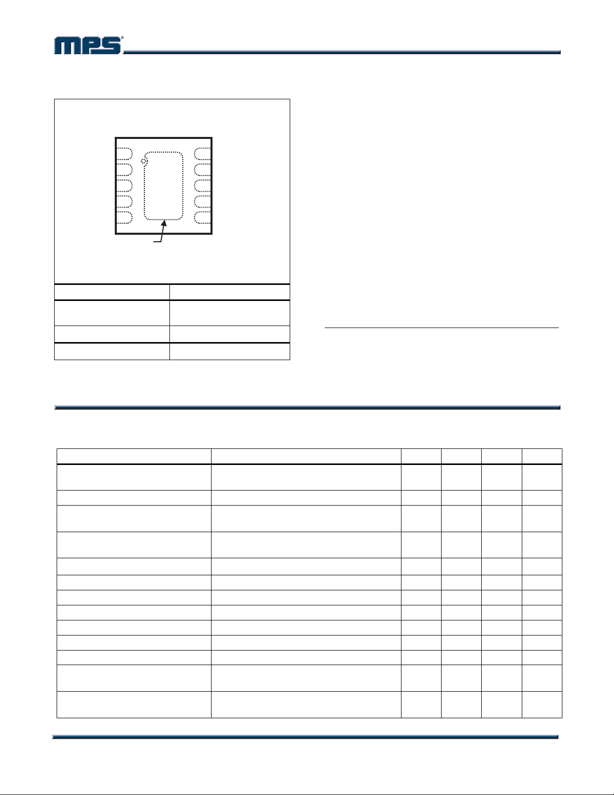
PACKAGE REFERENCE
TOP VIEW
FB
1
GND
2
SW
3
IN
4
BS
5
EXPOSED PAD
ON BACKSIDE
Part Number* Package
MP38115DQ
Temperature Top Marking
–40°C to +85°C
For Tape & Reel, add suffix –Z (e.g. MP38115DQ–Z)
*
For RoHS Compliant Packaging, add suffix –LF
(e.g. MP38115DQ–LF–Z)
EN/SYNC
10
GND
9
SW
8
IN
7
VCC
6
QFN10
(3mm x 3mm)
W2YW
ABSOLUTE MAXIMUM RATINGS
(1)
IN to GND ................................... –0.3V to +6.0V
VCC to GND ..............................
SW to GND..........................
............................
–2.5V to V
FB, EN/SYNC to GND ..................
BS to SW ....................................
–0.3V to + 6.0V
–0.3V to V
+ 2.5V for < 50ns
IN
+ 0.3V
IN
–0.3V to +6.5V
–0.3V to +6.5V
Junction Temperature............................... 150°C
Lead Temperature ....................................260°C
Storage Temperature ..............
Recommended Operating Conditions
–65°C to +150°C
(2)
Supply Volts VIN.............................. 1.1V to 5.5V
Supply Voltage V
Output Voltage V
......................... 2.7V to 5.5V
CC
................. 0.8V to 0.9 x VIN
OUT
Operating Temperature .............
Thermal Resistance
(3)
θ
–40°C to +85°C
θJC
JA
QFN10 (3mm x 3mm) ............. 50 ...... 12... °C/W
Notes:
1) Exceeding these ratings may damage the device.
2) The device is not guaranteed to function outside of its
operating conditions.
3) Measured on JESD51-7, 4-layer PCB..
ELECTRICAL CHARACTERISTICS
(4)
VCC = VEN = 3.6V, TA = +25°C, unless otherwise noted.
Parameters Condition Min Typ Max Units
V
= VCC
Supply Current
EN
VFB = 0.85V
Shutdown Current VEN = 0V, VCC = 5.5V 1 A
VCC Undervoltage Lockout
Threshold
VCC Undervoltage Lockout
Hysteresis
Rising Edge 2.59 2.69 V
210 mV
Regulated FB Voltage TA = +25°C 0.784 0.800 0.816 V
FB Input Current VFB = 0.85V ±50 nA
EN High Threshold –40°C TA +85°C 1.6 V
EN Low Threshold –40°C TA +85°C 0.4 V
Internal Soft-Start Time 120 µs
High-Side Switch On-Resistance ISW = 300mA 60 m
Low-Side Switch On-Resistance ISW = –300mA 60 m
V
= 0V; VCC = 5.5V, VIN = 5.5V
SW Leakage Current
BS Under Voltage Lockout
Threshold
EN
V
SW
1.8 V
= 0V or 5.5V
750 A
–10 10 A
MP38115 Rev. 0.92 www.MonolithicPower.com 2
8/11/2009 MPS Proprietary Information. Unauthorized Photocopy and Duplication Prohibited.
© 2009 MPS. All Rights Reserved.
Page 3
MP38115 – 4A, 5.5V SYNCHRONOUS STEP-DOWN SWITCHING REGULATOR
ELECTRICAL CHARACTERISTICS
(4)
(continued)
VIN = VEN = 3.6V, TA = +25°C, unless otherwise noted.
Parameters Condition Min Typ Max Units
High-Side Switch Current Limit Sourcing 6.5 A
Low-Side Switch Current Limit Sinking 3.5 A
Oscillator Frequency 1.2 1.5 1.8 MHz
Maximum Synch Frequency 2 MHz
Minimum Synch Frequency 1 MHz
Minimum On Time 50 ns
Maximum Duty Cycle 90 %
Thermal Shutdown Threshold Hysteresis = 20°C 150 °C
Note:
4) Production test at +25°C. Specifications over the temperature range are guaranteed by design and characterization.
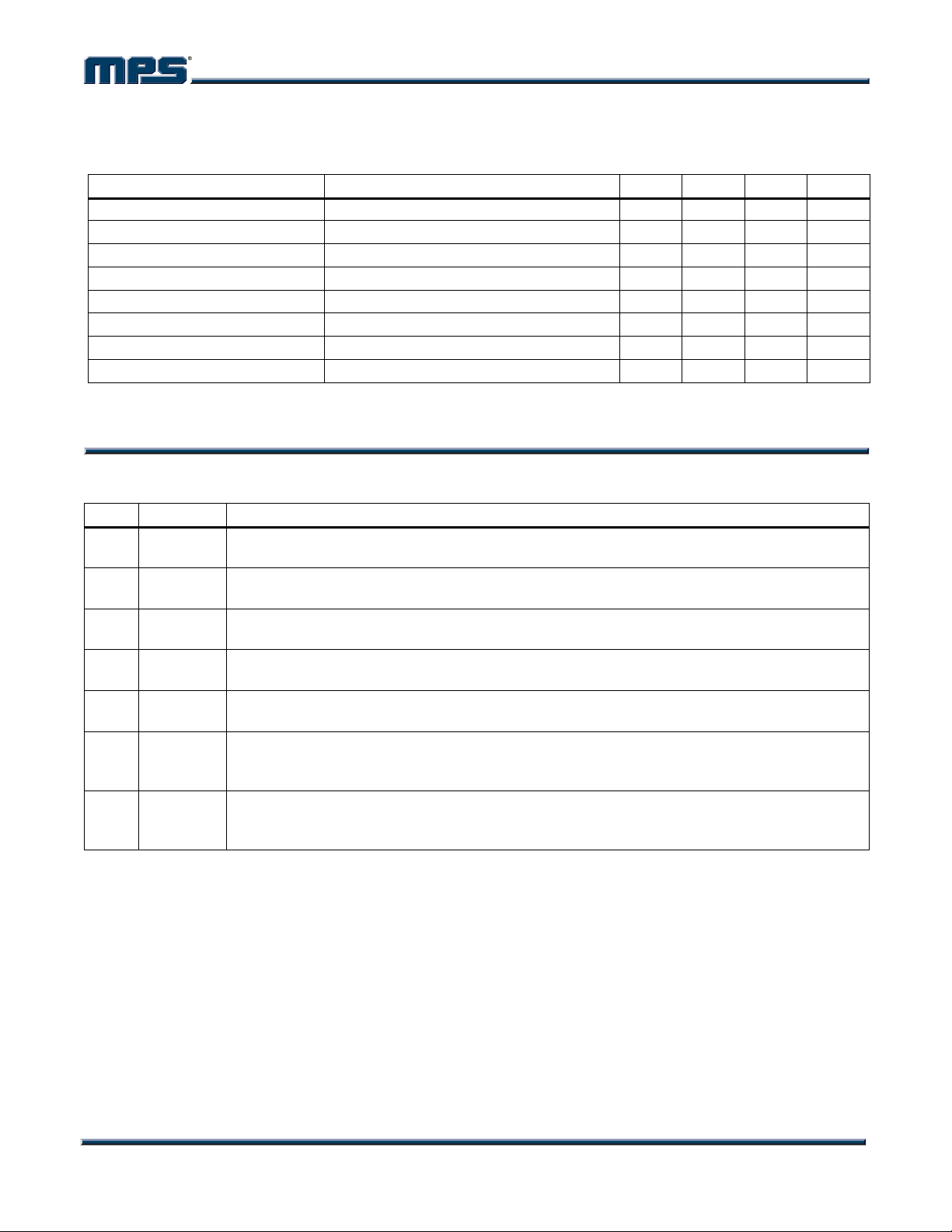
PIN FUNCTIONS
Pin # Name Description
6 VCC
4, 7 IN
3, 8 SW
2, 9 GND
5 BS
1 FB
10 EN/SYNC
Bias Supply. This supplies power to both the internal control circuit and the gate drivers. A
decoupling capacitor to ground is required close to this pin.
Input Supply. A decoupling capacitor to ground is required close to these pins to reduce
switching spikes.
Switch Node Connection to the Inductor. These pins connect to the internal high and lowside power MOSFET switches. All SW pins must be connected together externally.
Ground. Connect these pins with larger copper areas to the negative terminals of the input
and output capacitors.
Bootstrap. A capacitor between this pin and SW provides a floating supply for the high-side
gate driver.
Feedback. This is the input to the error amplifier. An external resistive divider connects this
pin between the output and GND. The voltage on the FB pin compares to the internal 0.8V
reference to set the regulation voltage.
Enable and Frequency Synchronization Input Pin. Forcing this pin below 0.4V shuts down
the part. Forcing this pin above 1.6V turns on the part. Applying a 1MHz to 2MHz clock
signal to this pin synchronizes the internal oscillator frequency to the external clock.
MP38115 Rev. 0.92 www.MonolithicPower.com 3
8/11/2009 MPS Proprietary Information. Unauthorized Photocopy and Duplication Prohibited.
© 2009 MPS. All Rights Reserved.
Page 4
MP38115 – 4A, 5.5V SYNCHRONOUS STEP-DOWN SWITCHING REGULATOR
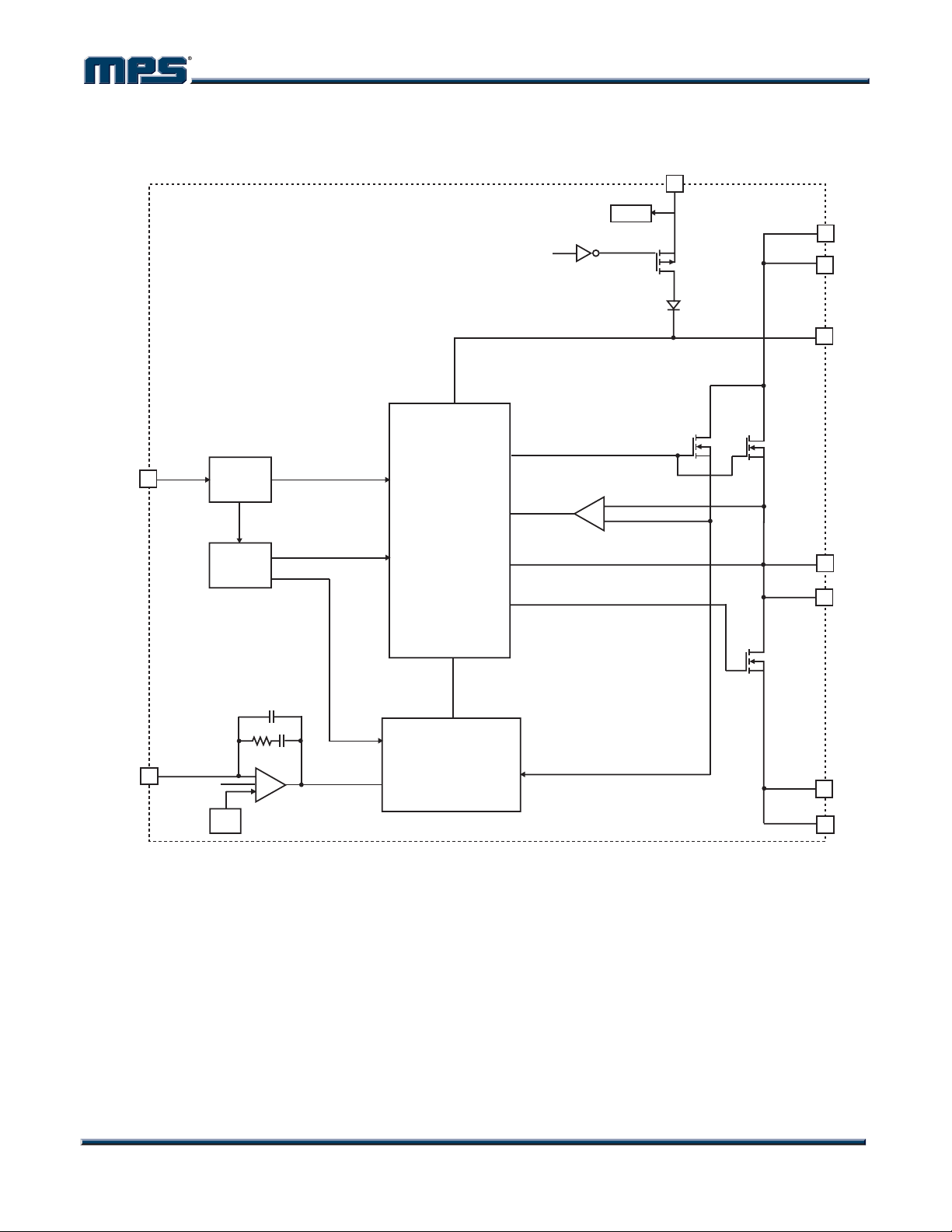
FUNCTIONAL BLOCK DIAGRAM
VCC
UVLO
IN
EN
IN
BS
EN/SYNC
FB
0.8V
SOFT
-START
EN/SYNC
LOGIC
EXCLK
OSC
1.2 MEG
EN
-+
0.5pF
CLK
SLOPE
17pF
LOGIC
PWM
CURRENT
COMPARATOR
SLOPE
COMPENSATION
-+
+
COMP
AND PEAK
CURRENT LIMIT
Figure 1—Functional Block Diagram (MP38115)
SW
SW
GND
GND
MP38115 Rev. 0.92 www.MonolithicPower.com 4
8/11/2009 MPS Proprietary Information. Unauthorized Photocopy and Duplication Prohibited.
© 2009 MPS. All Rights Reserved.
Page 5

MP38115 – 4A, 5.5V SYNCHRONOUS STEP-DOWN SWITCHING REGULATOR
FUNCTIONAL DESCRIPTION
PWM Control
The MP38115 is a constant frequency peakcurrent-mode control PWM switching regulator.
Refer to the functional block diagram. The high side
N-Channel DMOS power switch turns on at the
beginning of each clock cycle. The current in the
inductor increases until the PWM current
comparator trips to turn off the high side DMOS
switch. The peak inductor current at which the
current comparator shuts off the high side power
switch is controlled by the COMP voltage at the
output of feedback error amplifier. The
transconductance from the COMP voltage to the
output current is set at 11.25A/V.
This current-mode control greatly simplifies the
feedback compensation design by approximating
the switching converter as a single-pole system.
Only Type II compensation network is needed,
which is integrated into the MP38115. The loop
bandwidth is adjusted by changing the upper
resistor value of the resistor divider at the FB pin.
The internal compensation in the MP38115
simplifies the compensation design, minimizes
external component counts, and keeps the flexibility
of external compensation for optimal stability and
transient response.
Enable and Frequency Synchronization
(EN/SYNC PIN)
This is a dual function input pin. Forcing this pin
below 0.4V for longer than 4us shuts down the part;
forcing this pin above 1.6V for longer than 4µs turns
on the part. Applying a 1MHz to 2MHz clock signal
to this pin also synchronizes the internal oscillator
frequency to the external clock. When the external
clock is used, the part turns on after detecting the
first few clocks regardless of duty cycles. If any ON
or OFF period of the clock is longer than 4µs, the
signal will be intercepted as an enable input and
disables the synchronization.
exceeds the reference voltage of 0.8V. At this point
the reference voltage takes over at the noninverting error amplifier input. The soft-start time is
internally set at 120µs. If the output of the MP38115
is pre-biased to a certain voltage during startup, the
IC will disable the switching of both high-side and
low-side switches until the voltage on the internal
soft-start capacitor exceeds the sensed output
voltage at the FB pin.
Over Current Protection
The MP38115 offers cycle-to-cycle current limiting
for both high-side and low-side switches. The highside current limit is relatively constant regardless of
duty cycles. When the output is shorted to ground,
causing the output voltage to drop below 70% of its
nominal output, the IC is shut down momentarily
and begins discharging the soft start capacitor. It
will restart with a full soft-start when the soft- start
capacitor is fully discharged. This hiccup process is
repeated until the fault is removed.
Bootstrap (BST PIN)
The gate driver for the high-side N-channel DMOS
power switch is supplied by a bootstrap capacitor
connected between the BS and SW pins. When the
low-side switch is on, the capacitor is charged
through an internal boost diode. When the high-side
switch is off and the low-side switch turns on, the
voltage on the bootstrap capacitor is boosted above
the input voltage and the internal bootstrap diode
prevents the capacitor from discharging.
Soft-Start and Output Pre-Bias Startup
When the soft-start period starts, an internal current
source begins charging an internal soft-start
capacitor. During soft-start, the voltage on the softstart capacitor is connected to the non-inverting
input of the error amplifier. The soft-start period
lasts until the voltage on the soft-start capacitor
MP38115 Rev. 0.92 www.MonolithicPower.com 5
8/11/2009 MPS Proprietary Information. Unauthorized Photocopy and Duplication Prohibited.
© 2009 MPS. All Rights Reserved.
Page 6
MP38115 – 4A, 5.5V SYNCHRONOUS STEP-DOWN SWITCHING REGULATOR
APPLICATION INFORMATION
Output Voltage Setting
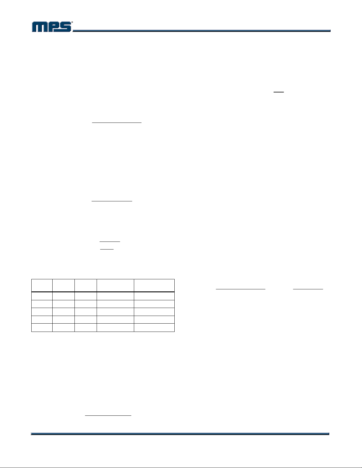
The external resistor divider sets the output
voltage (see Page 1, Schematic Diagram). The
feedback resistor R1 also sets the feedback loop
bandwidth with the internal compensation (refer
to description function). The relation between R1
and feedback loop bandwidth (f
capacitance (C
The feedback loop bandwidth (f
than 1/10
th
) is as follows:
O
1024.1
)K(1R
=Ω
×
O
of switching frequency of MP2107. In
the case of ceramic capacitor as C
set in the range of 50KHz and 150KHz for
optimal transient performance and good phase
margin. If an electrolytic capacitor is used, the
loop bandwidth is no higher than 1/4 of the ESR
zero frequency (f
For example, choose f
capacitor, C
O
). f
is given by:
ESR
1
2R C
π× ×
ESR O
=70KHz with a ceramic
C
f
ESR
ESR
=
=47F, R1 is estimated to be
400K. R2 is then given by:
R1
R2 =
V
0.8V
OUT
-1
Table 1—Resistor Selection vs.
Output Voltage Setting
Vout R1 R2 L
1.2V 400k 806k 0.47H-1H 47F
1.5V 400k 453k 0.47H-1H 47F
1.8V 400k 316k 0.47H-1H 47F
2.5V 400k 187k 0.47H-1H 47F
3.3V 400k 127k 0.47H-1H 47F
Inductor Selection
A 0.47µH to 1µH inductor with DC current rating at
least 25% higher than the maximum load current is
recommended for most applications. For best
efficiency, the inductor DC resistance shall be
<10m. See Table 2 for recommended inductors
and manufacturers. For most designs, the
inductance value can be derived from the following
equation:
OUT IN OUT
Vx(V-V)
L=
IN L OSC
VxIxf
), output
C
6
)F(C)KHz(fc
μ×
) is no higher
C
, it is usually
O
Cout
(Ceramic)
where I
L is Inductor Ripple Current. Choose
inductor ripple current approximately 30% of the
maximum load current, 4A.
The maximum inductor peak current is:
L
L(MAX) LOAD
I=I+
I
2
Under light load conditions, larger inductance is
recommended for improved efficiency.
Input Capacitor Selection
The input capacitor reduces the surge current
drawn from the input and the switching noise
from the device. The input capacitor impedance
at the switching frequency shall be less than
input source impedance to prevent high
frequency switching current passing to the input
source. Ceramic capacitors with X5R or X7R
dielectrics are highly recommended because of
their low ESR and small temperature coefficients.
For most applications, a 47µF capacitor is
sufficient.
Output Capacitor Selection
The output capacitor keeps output voltage ripple
small and ensures a stable regulation loop. The
output capacitor impedance shall be low at the
switching frequency. Ceramic capacitors with
X5R or X7R dielectrics are recommended. The
output ripple V
OUT
Δ≤
V x(ESR+ )
External Schottky Diode
For this part, an external schottky diode is
recommended to be placed close to "SW" and
"GND" pins, especially when the output current is
larger than 2A.
With the external schottky diode, the voltage
spike and negative kick on "SW" pin can be
minimized; moreover, the conversion efficiency
can also be improved a little.
For the external schottky diode selection, it's
noteworthy that the maximum reverse voltage
rating of the external diode should be larger than
the maximum input voltage. As for the current
rating of this diode, 0.5A rating should be
sufficient.
OUT is approximately:
OUT IN OUT
Vx(V-V) 1
IN OSC OSC 3
V xf xL 8xf xC
MP38115 Rev. 0.92 www.MonolithicPower.com 6
8/11/2009 MPS Proprietary Information. Unauthorized Photocopy and Duplication Prohibited.
© 2009 MPS. All Rights Reserved.
Page 7
MP38115 – 4A, 5.5V SYNCHRONOUS STEP-DOWN SWITCHING REGULATOR
Table 2—Suggested Surface Mount Inductors
Manufacturer
Wurth Electronics
TOKO
B1015AS-1R0N 1 11 6.9 8.4×8.3×4
Part
Number
744310055 0.55 4.5 14 7×6.9×3
744310095 0.95 7.4 11 7×6.9×3
Inductance
(μH)
Max DCR
(mΩ)
Current Rating
(A)
Dimensions
L x W x H (mm3)
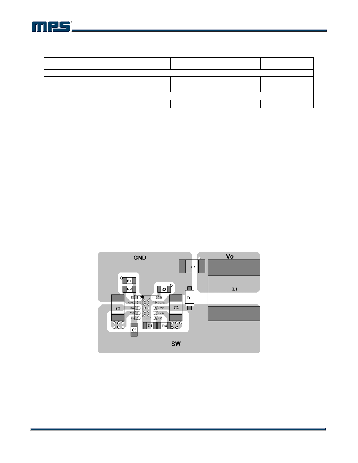
PCB Layout Guide
PCB layout is very important to achieve stable
operation. It is highly recommended to duplicate
EVB layout for optimum performance. If change
is necessary, please follow these guidelines as
follows. Here, the typical application circuit is
taken as an example to illustrate the key layout
rules should be followed.
1) For MP38115, a PCB layout with more than
(or) four layers is recommended.
2) The high current paths (GND, IN and SW)
should be placed very close to the device with
short, direct and wide traces.
3) For MP38115, two input ceramic capacitors (2
x (10F~22F)) are strongly recommended to be
placed on both sides of the MP38115 package
and keep them as close as possible to the “IN”
and “GND” pins.
4) An RC low pass filter is recommended for
VCC supply. The VCC decoupling capacitor must
be placed as close as possible to “VCC” pin and
“GND” pin.
5) The external feedback resistors shall be
placed next to the FB pin. Keep the FB trace as
short as possible. Don’t place test points on FB
trace if possible.
6) Keep the switching node SW short and away
from the feedback network.
Top Layer
MP38115 Rev. 0.92 www.MonolithicPower.com 7
8/11/2009 MPS Proprietary Information. Unauthorized Photocopy and Duplication Prohibited.
© 2009 MPS. All Rights Reserved.
Page 8
MP38115 – 4A, 5.5V SYNCHRONOUS STEP-DOWN SWITCHING REGULATOR
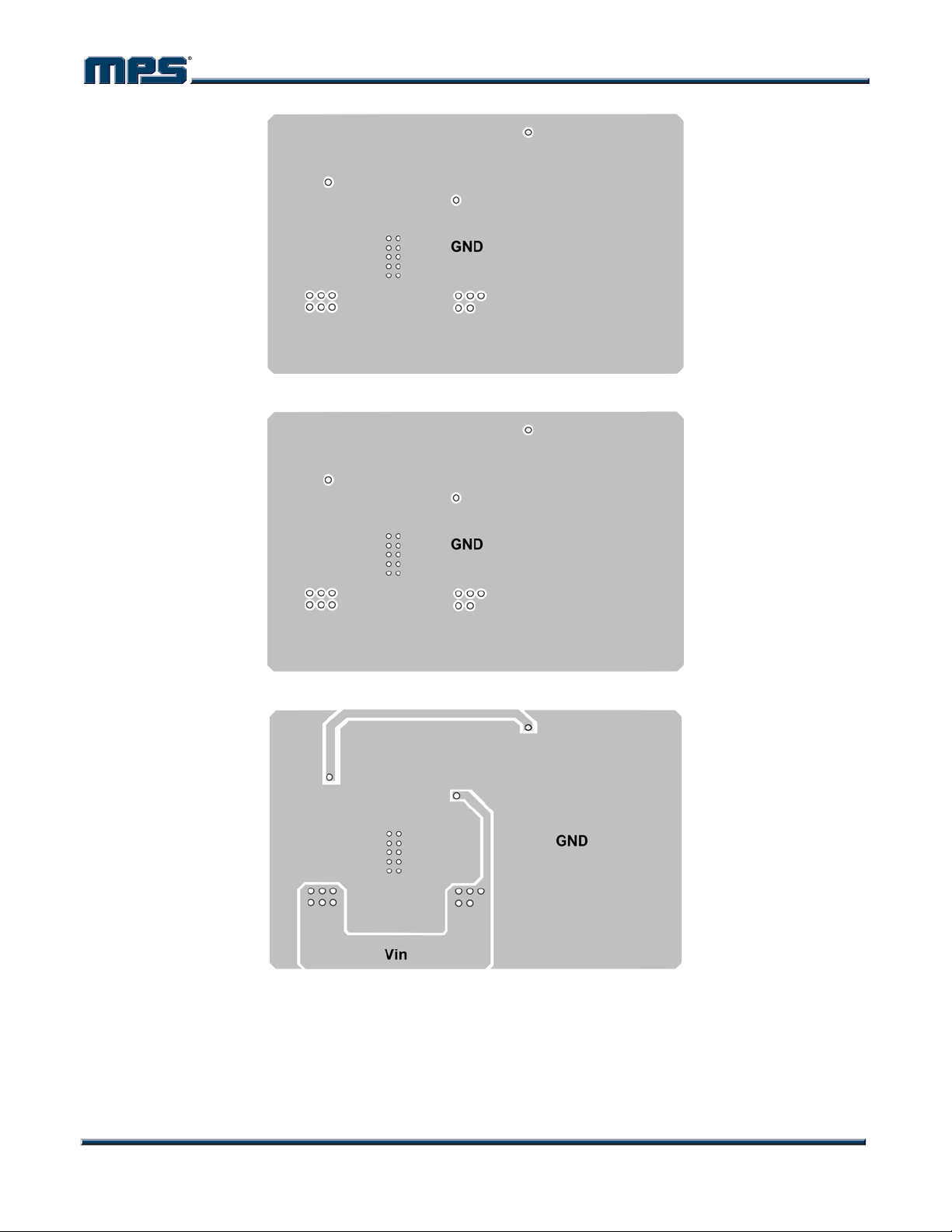
Inner Layer1
Inner Layer2
Bottom Layer
Figure2—Recommended PCB Layout of MP38115
MP38115 Rev. 0.92 www.MonolithicPower.com 8
8/11/2009 MPS Proprietary Information. Unauthorized Photocopy and Duplication Prohibited.
© 2009 MPS. All Rights Reserved.
Page 9
MP38115 – 4A, 5.5V SYNCHRONOUS STEP-DOWN SWITCHING REGULATOR
TYPICAL APPLICATION CIRCUITS
Vin
2.7V to 5.5V
R4
10
C1
22uF
C2
22uF
6
C4
1uF
10
R3
100k
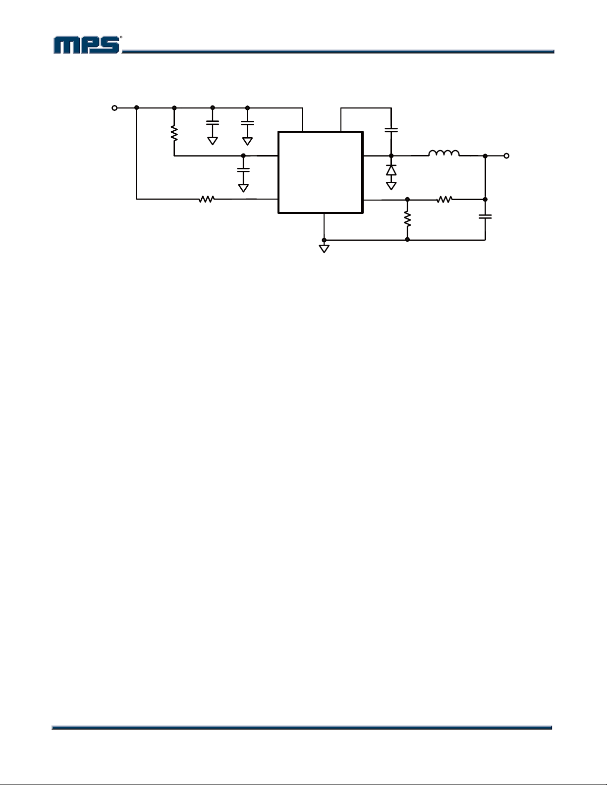
Figure3—Typical Application Circuit of MP38115
4,7 5
Vcc
MP38115
EN/SYNC
GND
2,9
C4
100nF
BSIN
SW
FB
3,8
D1
B0530
1
R2
316k
L1
1uH
Vout
1.8V/ 4A
R1
400k
C3
47uF
MP38115 Rev. 0.92 www.MonolithicPower.com 9
8/11/2009 MPS Proprietary Information. Unauthorized Photocopy and Duplication Prohibited.
© 2009 MPS. All Rights Reserved.
Page 10
MP38115 – 4A, 5.5V SYNCHRONOUS STEP-DOWN SWITCHING REGULATOR
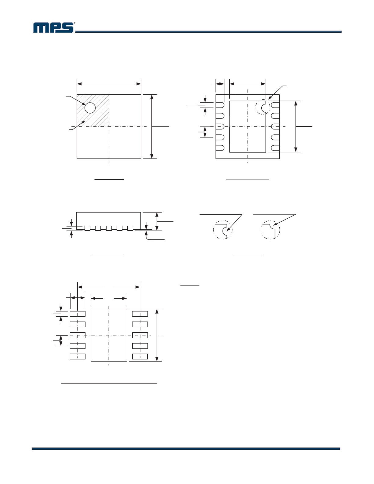
PACKAGE INFORMATION
2.90
3.10
PIN 1 ID
MARKING
QFN10 (3mm x 3mm)
0.30
0.50
0.18
0.30
1.45
1.75
PIN 1 ID
SEE DETAIL A
110
PIN 1 ID
INDEX AREA
0.20 REF
0.70
0.25
TOP VIEW
SIDE VIEW
2.90
1.70
0.00
0.05
2.90
3.10
0.50
BSC
6
5
BOTTOM VIEW
PIN 1 ID OPTION A
R0.20 TYP.
0.80
1.00
PIN 1 ID OPTION B
R0.20 TYP.
DETAIL A
NOTE:
1) ALL DIMENSIONS ARE IN MILLIMETERS.
2) EXPOSED PADDLE SIZE DOES NOT INCLUDE MOLD FLASH.
3) LEAD COPLANARITY SHALL BE 0.10 MILLIMETER MAX.
4) DRAWING CONFORMS TO JEDEC MO-229, VARIATION VEED-5.
5) DRAWING IS NOT TO SCALE.
2.25
2.55
0.50
RECOMMENDED LAND PATTERN
2.50
NOTICE: The information in this document is subject to change without notice. Users should warrant and guarantee that third
party Intellectual Property rights are not infringed upon when integrating MPS products into any application. MPS will not
assume any legal responsibility for any said applications.
MP38115 Rev. 0.92 www.MonolithicPower.com 10
8/11/2009 MPS Proprietary Information. Unauthorized Photocopy and Duplication Prohibited.
© 2009 MPS. All Rights Reserved.
Page 11

 Loading...