

Page 1

MP2625
All MPS parts are lead-free and adhere to the RoHS directive. For MPS green
status, please visit MPS website under Products, Quality Assurance page.
“MPS” and “The Future of Analog IC Technology” are registered trademarks of
Monolithic Power Systems, Inc.
2A Switching Charger with NVDC
Power Path Management
For Single Cell Li+ Battery
DESCRIPTION
The MP2625 is a monolithic switch mode
battery charger with power path management
for single-cell Li-ion batteries in a wide range of
tablet and other portable devices. It integrates a
synchronous BUCK regulator to provide
regulated voltage for powering the system
output and at the same time charging the
battery. This device supports both USB and
high power DC adapter input. In USB mode, the
input current limit can be programmed to
450mA or 825mA via the logic pins to cover the
USB2.0 and USB3.0 specifications. When the
adapter input is present, the input current can
also be limited in order to avoid overloading of
the DC adapter. Input current limit can be
programmed up to 2A.
The smart power path management allows
MP2625 to regulate the system voltage for
powering an external load and charging the
battery independently and simultaneously. This
allows immediate system operation even under
missing or deeply discharged battery. When the
input current limit is reached, the system load is
satisfied in priority, then the charger will take
the remaining current to charge the battery.
Additionally, the smart power path control
allows an internal connection from battery to the
system in order to supplement additional power
to the load in the event the system power
demand increases over the input limited power
or the input is removed.
FEATURES
4V to 14V Operating Input Voltage
Smart Power Path Management
Five Control Loops: Input Current Limit,
Input Voltage Limit, Constant Charge
Current, Terminal Battery Control and
Thermal Fold-Back.
1.6MHz Switching Frequency
Programmable Input Current Limit
Programmable Charge Current
Single Input for USB and AC adapter
Cover USB2.0 and USB3.0 Input
Specification
Fully Integrated Power Switches
No External Blocking Diode and Sense
Resistor Required
Charging Operation Indicator
Built-in Programmable Charging Timer
Thermal Limiting Regulation on Chip
Battery Temperature Monitor
Tiny Package Features Small Size
APPLICATIONS
Smart Phone
E-Book
GPS
Portable Media Player
Portable Hand-held Solution
Tablet PC
The MP2625 features high integration with all
the power switches included inside. No external
MOSFET, blocking diodes, or current sense
resistor is required.
Two status monitor output pins are provided to
indicate the battery charge status and power
source status. Other features include trickle
charge, battery temperature monitoring, timer
and thermal limiting regulation on chip.
MP2625 is available in QFN 3mmx4mm
package.
MP2625 Rev. 1.12 www.MonolithicPower.com 1
10/29/2013 MPS Proprietary Information. Patent Protected. Unauthorized Photocopy and Duplication Prohibited.
© 2013 MPS. All Rights Reserved.
Page 2
MP2625 – SINGLE CELL SWITCHING CHARGER WITH POWER PATH CONTROL
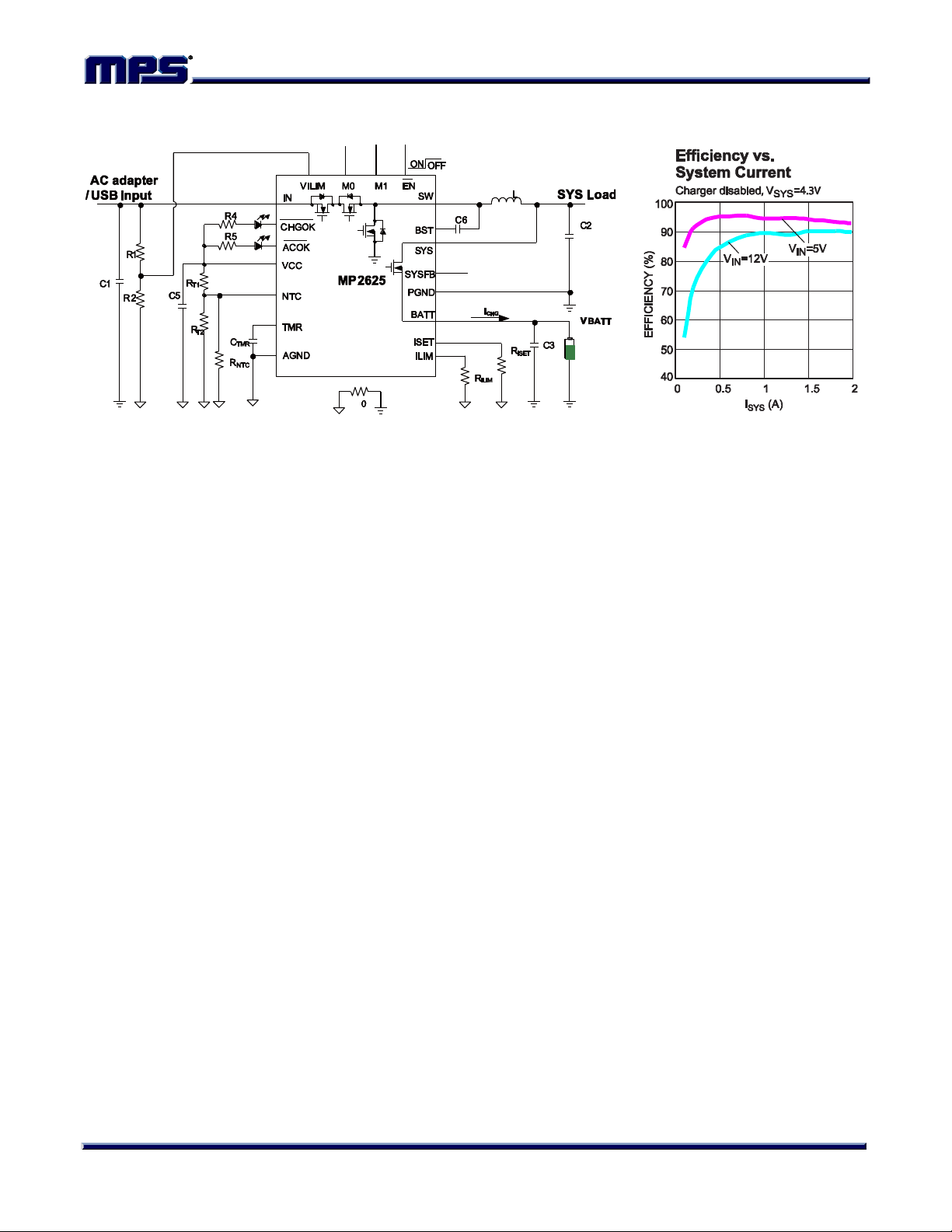
TYPICAL APPLICATION
MP2625 Rev. 1.12 www.MonolithicPower.com 2
10/29/2013 MPS Proprietary Information. Patent Protected. Unauthorized Photocopy and Duplication Prohibited.
© 2013 MPS. All Rights Reserved.
Page 3
MP2625 – SINGLE CELL SWITCHING CHARGER WITH POWER PATH CONTROL
Part Number*
Package
Top Marking
MP2625GL
QFN 3mmx4mm
MP2625
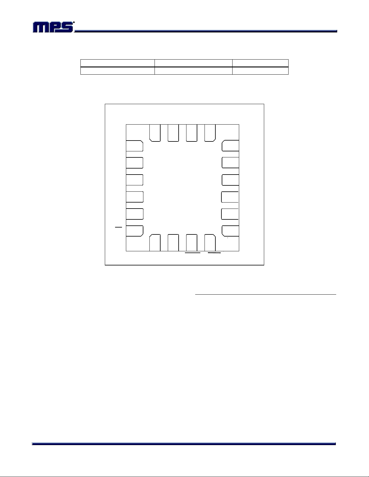
TOP VIEW
TMR
1
2
3
16
15
14
11
7 8 9 10
20
19
18
17
ILIM
PGND
EN
NTC
ISET
CHGOK ACOK
VCC
BST
VLIM
M0 M1
SYS
BATT
6
4
5
13
12
AGND
IN
SW
SW
SYSFB
Notes:
1) Exceeding these ratings may damage the device.
2) The maximum allowable power dissipation is a function of the
maximum junction temperature TJ (MAX), the junction-to-
ambient thermal resistance θ
JA
, and the ambient temperature
TA. The maximum allowable continuous power dissipation at
any ambient temperature is calculated by PD (MAX) = (T
J
(MAX)-T
A
)/θ
JA
. Exceeding the maximum allowable power
dissipation will cause excessive die temperature, and the
regulator will go into thermal shutdown. Internal thermal
shutdown circuitry protects the device from permanent
damage.
3) The device is not guaranteed to function outside of its
operating conditions.
4) Measured on JESD51-7, 4-layer PCB.
ORDERING INFORMATION
* For Tape & Reel, add suffix –Z (e.g. MP2625GL–Z);
PACKAGE REFERENCE
ABSOLUTE MAXIMUM RATINGS
IN, SW ........................................ -0.3V to +20V
BATT, SYS .................................... -0.3V to +6V
BST ............................................. -0.3V to +26V
All Other Pins ................................. -0.3V to +6V
Continuous Power Dissipation (TA = +25°C)
QFN20 3mmx4mm .................................... 2.6W
Junction Temperature .............................. 150C
Lead Temperature ................................... 260C
Storage Temperature.................–65°C to 150°C
Recommended Operating Conditions
Supply Voltage VIN .......................... 4.5V to 12V
Operating Junction Temp. (TJ) .... -40°C to +125°C
MP2625 Rev. 1.12 www.MonolithicPower.com 3
10/29/2013 MPS Proprietary Information. Patent Protected. Unauthorized Photocopy and Duplication Prohibited.
© 2013 MPS. All Rights Reserved.
(1)
Thermal Resistance
(4)
θ
JA
θ
JC
QFN20 3mmx4mm ................. 48 ...... 11 ... C/W
(2)
(3)
Page 4
MP2625 – SINGLE CELL SWITCHING CHARGER WITH POWER PATH CONTROL
Parameters
Symbol
Condition
Min
Typ
Max
Units
Input Power (IN)
IN Operating Range
VIN
4.0
14
(5)
V
IN Under Voltage Lockout
Threshold
Rising
3.65
3.8
3.95
V
Falling
3.35
3.5
3.65
V
IN vs. BATT Threshold
Rising
270
310
350
mV
Falling
70
110
150
mV
BST Voltage Threshold
V
BST-VSW
Rising
2.75
2.9
3.05
V
Falling
2.6
2.75
2.9
V
Switching Frequency
1.4
1.6
1.8
MHz
Input Current Limit
IIN
USB2.0 Mode
400
450
500
mA
USB3.0 Mode
750
825
900
mA
Default Mode
1840
2000
2160
mA
Programmable Mode,
R
ILIM
=23k
1840
2000
2160
mA
Input Current Limit Reference
Voltage
V
ILIM
1.1
1.14
1.18
V
High-side NMOS On Resistance
R
H_DS(ON)
Include the BLOCK FET
120
130
mΩ
Low-side NMOS On Resistance
RL_
DS(ON)
80
100
mΩ
High-side NMOS Peak Current limit
3 4 5 A Input Voltage Clamp Threshold
V
VLIM
Voltage on VLIM
1.49
1.52
1.55
V
Input Quiescent Current
IIN
Charger Enabled, USB2.0 Mode
2.4 5 mA
Charger Enabled, USB3.0
Mode
2.8 5 mA
Charger Enable, Programmable
Mode
3.8 5 mA
Charger Enabled, Default Mode
3.8 5 mA
Disabled, EN=0V
3 5
uA
SYS to IN reverse current
blocking
SYS=SW=4.5V,VIN=0V, monitor
VIN leakage
0.01
0.2
uA
SYS Output
Minimum SYS Regulation
Voltage
V
SYS
SYS voltage @ V
BATT
≤3.4V,
SYSFB float
3.45
3.6
3.75
V
SYS Regulation Voltage
V
SYS
3.4V<V
BATT
≤4.2V, SYSFB float
BATT Float
3.5
V
BATT
+
0.2V
4.5
V
User Programmed by SYSFB
3.5
4.4
V
SYS Reference Voltage
V
SYS_REF
1.135
1.152
1.170
V
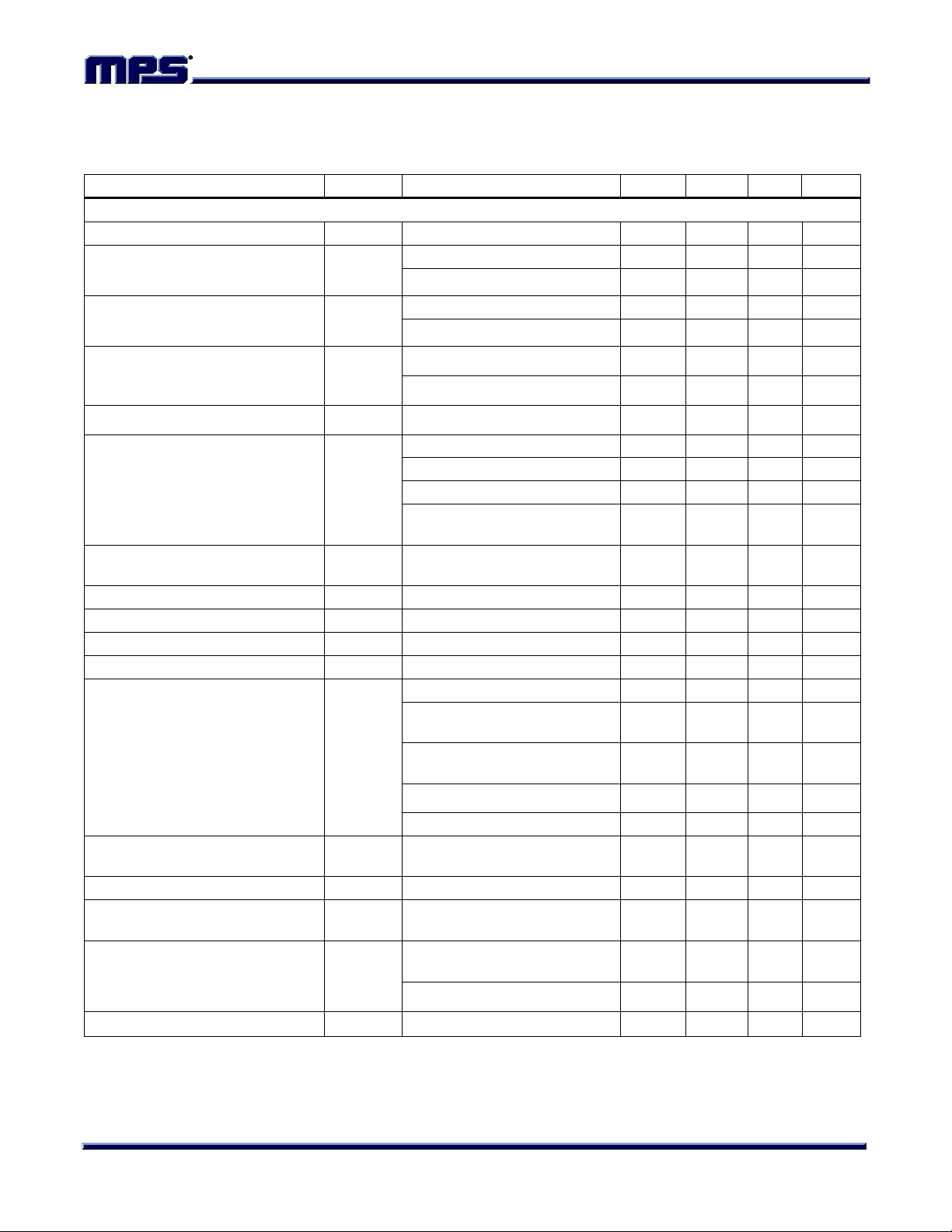
ELECTRICAL CHARACTERISTICS
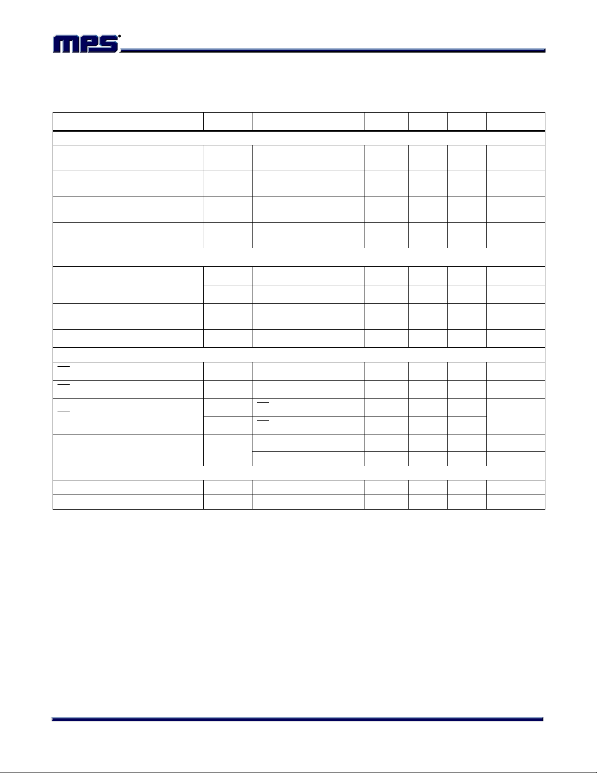
VIN = 5.0V, TA = 25C, unless otherwise noted.
MP2625 Rev. 1.12 www.MonolithicPower.com 4
10/29/2013 MPS Proprietary Information. Patent Protected. Unauthorized Photocopy and Duplication Prohibited.
© 2013 MPS. All Rights Reserved.
Page 5
MP2625 – SINGLE CELL SWITCHING CHARGER WITH POWER PATH CONTROL
Parameters
Symbol
Condition
Min
Typ
Max
Units
BATT to SYS Resistance
VIN=0V, I
SYS
=200mA,
V
BATT
=4.2V
0.04
0.05
Ω
BATT to SYS Current Limit
V
SYS>VBATT
–800mV
3 A
SYS short
200
mA
Battery Charger
Terminal Battery Voltage
V
BATT
V
BATT>VRECH
, I
CHG≤IBF,
SYSFB float
4.168
4.2
4.232
V
V
SYS
<4.2V Programmed
by SYSFB Pin
V
SYS
-
0.04 x IBF
V
Recharge Threshold at V
BATT
V
RECH
SYSFB Float
3.9
4.0
4.1
V
SYSFB programmed
3.85
3.95
4.05
V
Recharge Hysteresis
85
mV
Trickle Charge Threshold
2.9 3 3.1
V
Trickle Charger Hysteresis
200
mV
Trickle Charge Current
I
TRICKLE
10%
ICC
Termination Charger Current
IBF
5%
10%
15%
ICC
IBF Maximum Limit
150
200
mA
Constant Current Mode Charge
Current
ICC
R
ISET
=1.05k
1.8
2.0
2.2
A
R
ISET
=1.53k
1.26
1.4
1.54
A
R
ISET
=4.6k
0.405
0.45
0.495
A
ISET Reference Voltage
1.1
1.15
1.2
V
Battery UVLO
Rising
2.4
2.6
2.8 V
Falling
2.2
2.4
2.6
V
Idea Diode Regulation Voltage
V
SYS
Supplement Mode
V
BATT
-
65mV
mV
BATT Leakage Current
I
BATT
V
BATT
=4.2V, SYS float,
VIN=PGND
20
30
µA
ACOK
__________
, CHGOK
_____________
ACOK
__________
, CHGOK
_____________
Pin Output Low
Voltage
Sinking 5mA
270
350
mV
ACOK
__________
,CHGOK
_____________
Pin Leakage Current
Connected to 3.3V
0.1
0.5
uA
Timer
Trickle Charge Time
C
TMR
=0.1µF, I
CHG
=1A
45
Min
Total Charge Time
C
TMR
=0.1µF, I
CHG
=1A
6.5
Hour
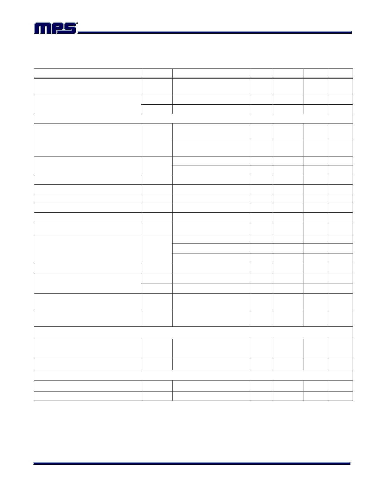
ELECTRICAL CHARACTERISTICS (continued)
VIN = 5.0V, TA = 25C, unless otherwise noted.
MP2625 Rev. 1.12 www.MonolithicPower.com 5
10/29/2013 MPS Proprietary Information. Patent Protected. Unauthorized Photocopy and Duplication Prohibited.
© 2013 MPS. All Rights Reserved.
Page 6
MP2625 – SINGLE CELL SWITCHING CHARGER WITH POWER PATH CONTROL
Parameters
Symbol
Condition
Min
Typ
Max
Units
Negative Temperature Coefficient (NTC) Control
NTC Low Temp Rising Threshold
V
THL
R
NTC
=NCP18XH103F
0°C
63
65
67
%VCC
Hysteresis on Low Temp
Threshold
35 mV
NTC High Temp Falling
Threshold
V
THH
R
NTC
=NCP18XH103F,
50°C
32
33.5
35
%VCC
Hysteresis on High Temp
Threshold
70 mV
VCC Supply
VCC UVLO
Rising
3.15
3.35
3.55
V
Falling
2.8 3 3.2
V
VCC Output Voltage
0mA<I
VCC
<25mA,
VIN=6V
4.3
4.5
4.6
V
VCC Short Circuit Current Limit
40 mA
Logic
EN
Input Low Voltage
0.4
V
EN
Input High Voltage
1.5
V
EN
Input Current
EN
=4V
4 8
μA
EN
=0V
-0.5
-0.1
M0, M1
Logic High
1.5
V
Logic Low
0.4
V
Protection
Thermal Limit Temperature
120 °C
Thermal Shutdown
150 °C
ELECTRICAL CHARACTERISTICS (continued)
VIN = 5.0V, TA = 25C, unless otherwise noted.
Notes:
5) Using a inductor with the saturation current larger than 6A when applying the part with higher than 12V input.
MP2625 Rev. 1.12 www.MonolithicPower.com 6
10/29/2013 MPS Proprietary Information. Patent Protected. Unauthorized Photocopy and Duplication Prohibited.
© 2013 MPS. All Rights Reserved.
Page 7

MP2625 – SINGLE CELL SWITCHING CHARGER WITH POWER PATH CONTROL
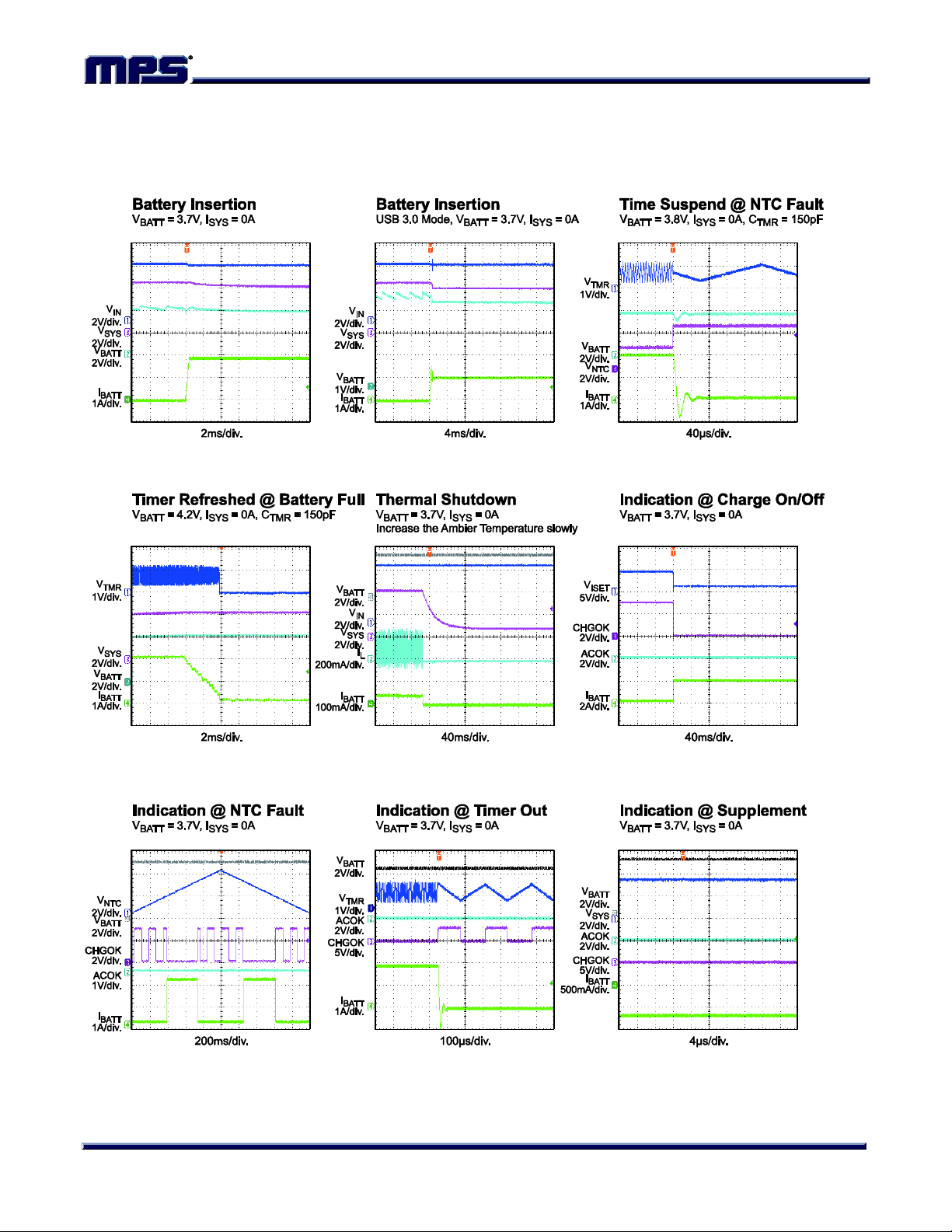
TYPICAL PERFORMANCE CHARACTERISTICS
VIN = 5.0V, V
V
Clamp=4.5V, L = 1.2 µH, TA = +25ºC, unless otherwise noted.
IN
= Full Range, Default Mode, IIN Limit=2A, V
BATT
SYS
=4.4V, R6 and R7 are float, I
CHG
=2A,
MP2625 Rev. 1.12 www.MonolithicPower.com 7
10/29/2013 MPS Proprietary Information. Patent Protected. Unauthorized Photocopy and Duplication Prohibited.
© 2013 MPS. All Rights Reserved.
Page 8
MP2625 – SINGLE CELL SWITCHING CHARGER WITH POWER PATH CONTROL
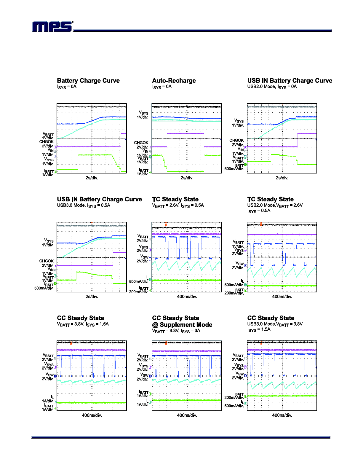
TYPICAL PERFORMANCE CHARACTERISTICS (continued)
VIN = 5.0V, V
V
Clamp=4.5V, L = 1.2 µH, TA = +25ºC, unless otherwise noted.
IN
= Full Range, Default Mode, IIN Limit=2A, V
BATT
=4.4V, R6 and R7 are float, I
SYS
CHG
=2A,
MP2625 Rev. 1.12 www.MonolithicPower.com 8
10/29/2013 MPS Proprietary Information. Patent Protected. Unauthorized Photocopy and Duplication Prohibited.
© 2013 MPS. All Rights Reserved.
Page 9
MP2625 – SINGLE CELL SWITCHING CHARGER WITH POWER PATH CONTROL
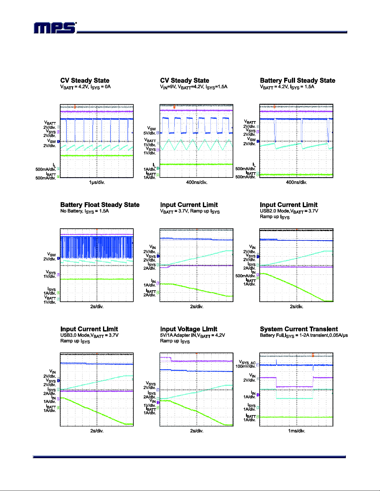
TYPICAL PERFORMANCE CHARACTERISTICS (continued)
VIN = 5.0V, V
L = 1.2 µH, TA = +25ºC, unless otherwise noted.
= Full Range, Default Mode, IIN Limit=2A, V
BATT
=4.4V, R6 and R7 are float, I
SYS
CHG
=2A,
MP2625 Rev. 1.12 www.MonolithicPower.com 9
10/29/2013 MPS Proprietary Information. Patent Protected. Unauthorized Photocopy and Duplication Prohibited.
© 2013 MPS. All Rights Reserved.
Page 10
MP2625 – SINGLE CELL SWITCHING CHARGER WITH POWER PATH CONTROL
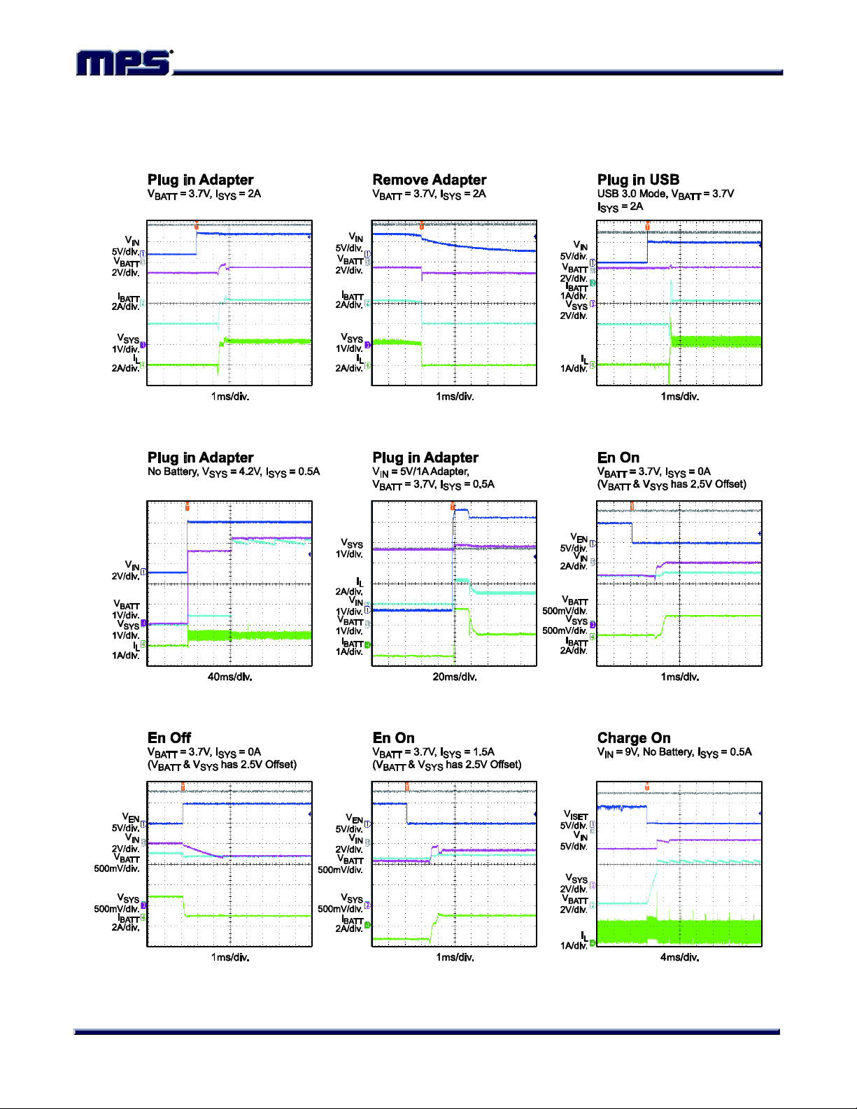
TYPICAL PERFORMANCE CHARACTERISTICS (continued)
VIN = 5.0V, V
L = 1.2 µH, TA = +25ºC, unless otherwise noted.
= Full Range, Default Mode, IIN Limit=2A, V
BATT
=4.4V, R6 and R7 are float, I
SYS
CHG
=2A,
MP2625 Rev. 1.12 www.MonolithicPower.com 10
10/29/2013 MPS Proprietary Information. Patent Protected. Unauthorized Photocopy and Duplication Prohibited.
© 2013 MPS. All Rights Reserved.
Page 11
MP2625 – SINGLE CELL SWITCHING CHARGER WITH POWER PATH CONTROL
TYPICAL PERFORMANCE CHARACTERISTICS (continued)
VIN = 5.0V, V
L = 1.2 µH, TA = +25ºC, unless otherwise noted.
= Full Range, Default Mode, IIN Limit=2A, V
BATT
=4.4V, R6 and R7 are float, I
SYS
CHG
=2A,
MP2625 Rev. 1.12 www.MonolithicPower.com 11
10/29/2013 MPS Proprietary Information. Patent Protected. Unauthorized Photocopy and Duplication Prohibited.
© 2013 MPS. All Rights Reserved.
Page 12
MP2625 – SINGLE CELL SWITCHING CHARGER WITH POWER PATH CONTROL
Package
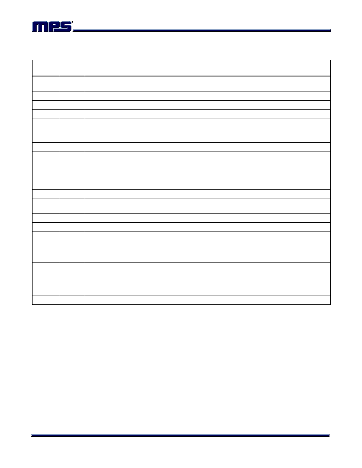
Pin #
Name
Description
1
BST
Bootstrap. A capacitor is connected between SW and BST pin to form a floating supply
across the power switch driver to drive the power switch’s gate above the supply voltage.
3
IN
Power input of the IC from adapter or USB.
2,4
SW
Switch output.
5
PGND
Power ground.
6
EN
_____
Function logic control pin of the IC. Logic low to enable the part and logic high to disable the
part. 7 M0
Mode Select Input Pin, in combination with M1 pin, setting the input current limit mode.
8
M1
Mode Select Input Pin, in combination with M0 pin, setting the input current limit mode.
9
CHGOK
_____________
Open drain output. It is pulled low during charging. And it is pulled high through an external
resistor to VCC to indicate charge completed.
10
ACOK
__________
Open drain output. It is pulled low to indicate the presence of a valid input power supply.
Otherwise, it is pulled high through an external resistor to VCC to indicate invalid input or
removed input.
11
AGND
Analog ground.
12
SYSFB
SYS voltage program pin. Connect a resistor divider from the pin to SYS and AGND to
program the system output voltage. Leave the pin float to disable the function.
13
SYS
DC-DC regulator output to power the system load and charge the battery.
14
BATT
Positive battery terminal.
15
ISET
Charge current program pin. A resistor from the pin to AGND can program the charge
current during CC charge. Float the pin will disable the charge function.
16
NTC
Thermistor input. Connect a resistor from this pin to VCC and the thermistor from this pin to
ground. The thermistor is usually inside the battery pack.
17
ILIM
Input current limit program pin. A resistor from the pin to AGND can program the input
current limit with adapter input.
18
TMR
Set timer out period. Connect TMR pin to AGND to disable the internal timer.
19
VLIM
Input voltage clamp program pin.
20
VCC
Supply voltage of the IC.
PIN FUNCTIONS
MP2625 Rev. 1.12 www.MonolithicPower.com 12
10/29/2013 MPS Proprietary Information. Patent Protected. Unauthorized Photocopy and Duplication Prohibited.
© 2013 MPS. All Rights Reserved.
Page 13
MP2625 – SINGLE CELL SWITCHING CHARGER WITH POWER PATH CONTROL
Driver
IN
SW
C
L
HSG
LSG
BST
SYS
V
BAT
x 2
Charge
Pump
BATT
SYS
EA
EA
SYSFB
SYSFB1
Max(A,B)
VBATT+200mV
EAO
Converter
control
4 0
mO
BATTFB
VREF
ILIM
M
1
M
0
Trim
SYS
BATT
Ideal diode
regulation
VTH
Battery switch
current limit
ISET
VIN
3.5 V coarse
LDO &
3.0 V UVLO
EN
VCC
4.5V LDO
VBG
3.8
V UVLO
VBG
VIN
UVLO
GND
NTCTMRACOKCHGOK
EN
EN
1.5V
EAO
VREF_CC
CC/ CV linear
charger
VLIM
3.6V
SYSFB1
SYSFB
BATTFB
Iref
Input current
limit reference
selector
Charger Control & Chip Logic
Bandgap
& Bias
EA
SYSFB
VBG
OPERATION
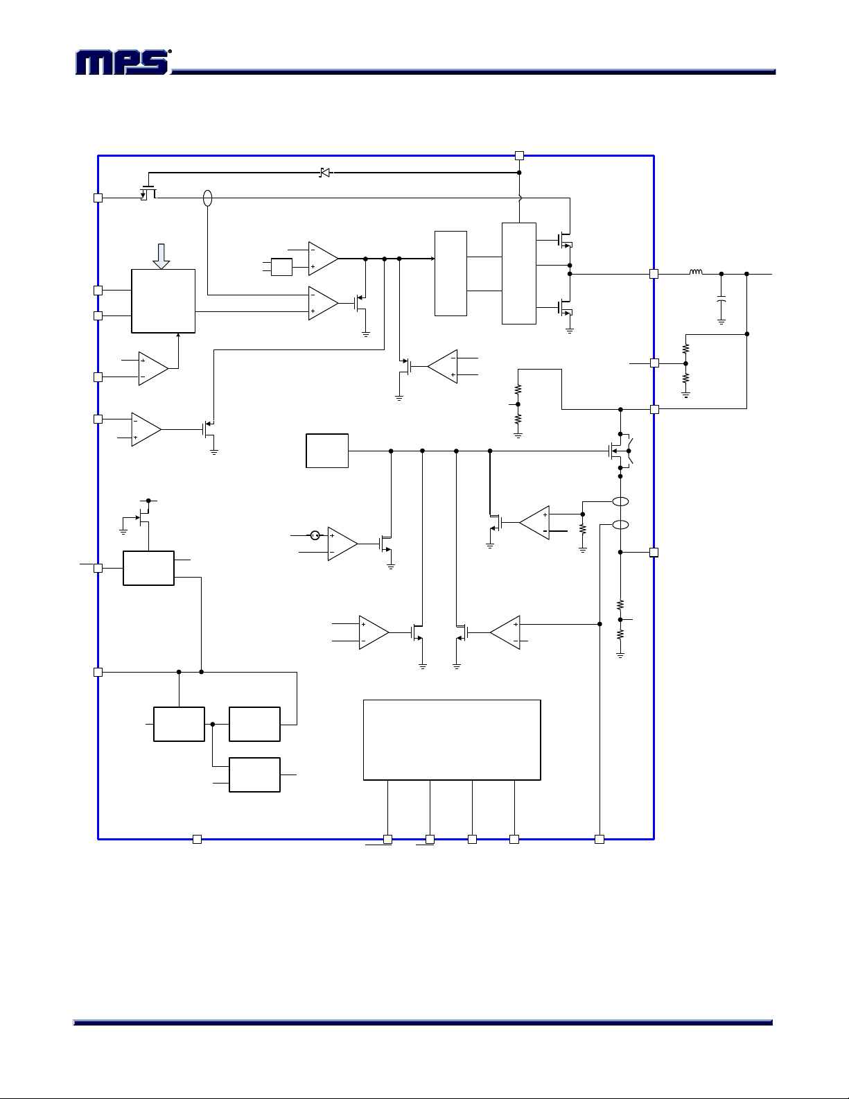
Figure 1—Function Block Diagram
MP2625 Rev. 1.12 www.MonolithicPower.com 13
10/29/2013 MPS Proprietary Information. Patent Protected. Unauthorized Photocopy and Duplication Prohibited.
© 2013 MPS. All Rights Reserved.
Page 14
MP2625 – SINGLE CELL SWITCHING CHARGER WITH POWER PATH CONTROL
4.4V
4.2V
3.6V
4.2V3.4V
200mV
V
BATT
V
SYS
Introduction
The MP2625 is a switching charger IC, with
integrated smart power path management for
powering the system and charging a single cell
battery simultaneously and independently.
The MP2625 includes a high-voltage (up to 14V)
input DC-DC step down converter for wide range
of DC sources and USB inputs. It has precision
average input current limit to make maximum use
of the allowable input power. This feature allows
fast charging when powering from an USB port,
and ensures the input current never exceeds the
input power specification especially when the
input power comes from a USB port. Additionally,
the input current limit threshold can be
programmed by logic inputs or a resistor to
ground from the ILIM pin.
The MP2625 implements an on-chip 40mΩ
MOSFET which works as a full-featured linear
charger with trickle charge, high accuracy
constant current and constant voltage charge,
charge termination, auto recharge, NTC monitor,
built-in timer control, charge status indication,
and thermal protection. The charge current can
be programmed by an external resistor
connected from the ISET pin to AGND. The IC
limits the charge current when the die
temperature exceeds 120°C.
The 40mΩ MOSFET works as an ideal diode to
connecting the battery to the system load when
the input power is not enough to power the
system load. When the input is removed, the
40mΩ MOSFET is turned on allowing the battery
to power up the system.
the combination of the system load and battery
charger. The regulator contains input current
measurement and control scheme to ensure the
average input current remains below the level
programmed via ILIM pin or logic inputs M0&M1.
This meets the adapter capacity limit or stays in
compliance with USB specification.
When the input voltage is higher than UVLO and
310mV higher than the battery voltage, input
voltage OK signal is active (ACOK
——————
turns low) and
the DC-DC converter soft-starts. If the input
power is sufficient to supply the combination of
the system load and battery charger, and the
input current limit loop is not triggered. The
converter output voltage V
1) If BATT>3.4V, V
SYS
will be regulated:
SYS
is approximately 0.2V
above the battery voltage to minimize the power
loss of the battery charger during fast charging.
2) If BATT<3.4V, V
is fixed at 3.6V to power
SYS
the system immediately even when a drained
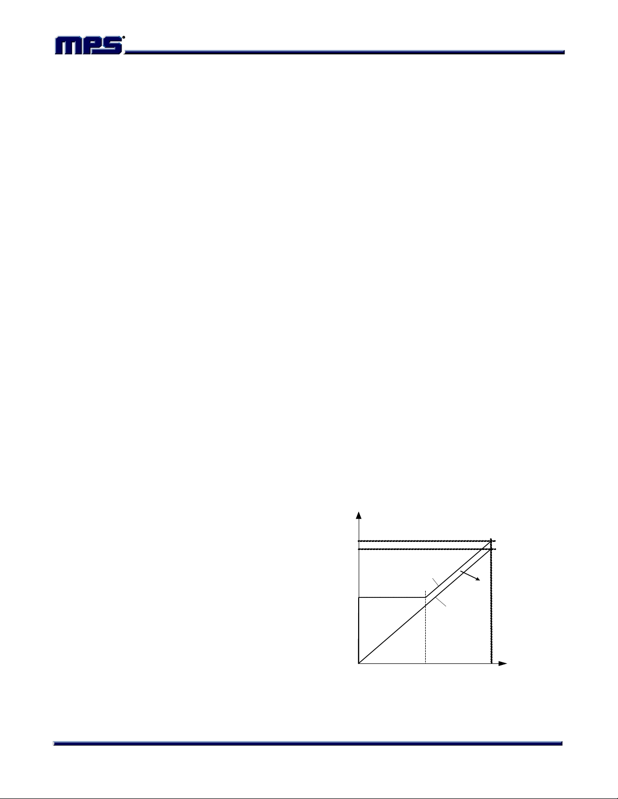
battery is inserted to be charged. Figure 2 shows
the relationship of V
SYS
vs. V
BATT.
System voltage can also be regulated to any
value between 3.6V to 4.4V by using a resistor
divider on the SYSFB pin. This is shown as R6
and R7 in Figure 9. If the SYSFB is left floating,
the system program is invalid, and V
SYS
is
regulated as Figure 2.
The converter adopts fixed off-time control to
extend the duty cycle (close to 100%) when the
input of the converter is close to V
SYS.
With smart power path management, the system
load is satisfied in priority then the remaining
current is used to charge the battery. The
MP2625 will reduce charging current or even use
power from the battery to satisfy the system load
when its demand is over the input power
capacity.
Figure 1 shows the function block diagram of
MP2625.
DC-DC Step Down Converter
The DC-DC converter is a 1.6MHz constant
frequency step-down switching regulator to
Figure 2 — SYS Regulation Output
provide the input power to the SYS, which drives
MP2625 Rev. 1.12 www.MonolithicPower.com 14
10/29/2013 MPS Proprietary Information. Patent Protected. Unauthorized Photocopy and Duplication Prohibited.
© 2013 MPS. All Rights Reserved.
Page 15

MP2625 – SINGLE CELL SWITCHING CHARGER WITH POWER PATH CONTROL
IN_LIM
ILIM
40000
I =1.14 (mA)
R (kΩ)
Close to 100% duty operation, BST refresh
operation makes sure the driver voltage of the
HS will be charged by turning on the LS until
negative IL hit about 400mA. If the input power is
insufficient to supply the combination of the
system load and battery charger, the DC-DC
converter will limit the total power requirement by
restricting the input voltage, input current and the
peak current through the MOSFET. The power
path management will reduce the charge current
to satisfy the external system load in priority.
According to this feature, the USB specification is
always satisfied first. Even if the charge current is
set larger than the USB input current limit, the
real charge current will be reduced as needed.
Input Limit State
If the input power is insufficient to supply the
combination of the system load and battery
charger, the MP2625 implements three input limit
control loops to reduce the charge current and
satisfy the external system load in priority. The
input in this case might be limited as follows:
input current limit, input voltage limit and DC-DC
peak current limit.
Input Current Limit: When the system current is
higher than the programmed input current limit
the input current limit loop takes the control of the
converter and regulates the input current at
constant value. When the battery voltage is over
3.4V, the output voltage (V
) will drop down
SYS
according to the increase of the system current,
and the charge current drops down after the
BATT-to-SYS switch (40mΩ MOSFET) is fully on
according to V
dropping down. During this
SYS
process, the system voltage is slightly higher
than V
. When the battery voltage is lower
BATT
than 3.4V, to maintain the minimum system
voltage and ensure the system operation, the
input current limit control will pull down the
charge current directly to reduce the load of the
converter so that the system current is satisfied
in priority.
Input Voltage Limit: A resistor divider from IN pin
to VLIM pin to AGND is used for the input voltage
limit control. When the voltage on VLIM pin hits
the reference voltage of 1.52V, the output of the
input voltage limit error amplifier will drop in
to control the operation duty. In this mode, the
input voltage will be clamped according to the
value set by the resistor divider. The control to
the system voltage and charge current is the
same as the one explained in the input current
limit. Charge current drops down to satisfy the
system current request first. This feature
provides a second protection to the input power
and ensures the safe operation of the input
adapter. Even if a wrong adapter is inserted, the
MP2625 can continue operation, providing the
maximum power to its load. User can program
the input voltage limit value through the resistor
divider from IN to VLIM to AGND.
Peak Current Limit: The peak current of the high
side switch of the DC-DC converter is sensed
during every cycle, it is compared to the
reference 4A, if the peak current hits the
threshold, the peak current limit mode is
triggered. The control of the charge current is the
same with the above two limits.
Input Current Limit Setting
The current at ILIM is a precise fraction of the
adapter input current. When a programming
resistor is connected from ILIM to AGND, the
voltage on ILIM represents the average input
current of the PWM converter. And the input
current approaches the programmed limit, ILIM
voltage reaches 1.14V.
The average input current limit can be set
through the resistor connecting from ILIM to
AGND according to the following expression:
When USB input, the input current limit is set
internally and the programmed value is invalid.
The MP2625 provides typical of 450mA input
current limit for USB2.0 specification and a
typical of 825mA for USB3.0 specification
respectively.
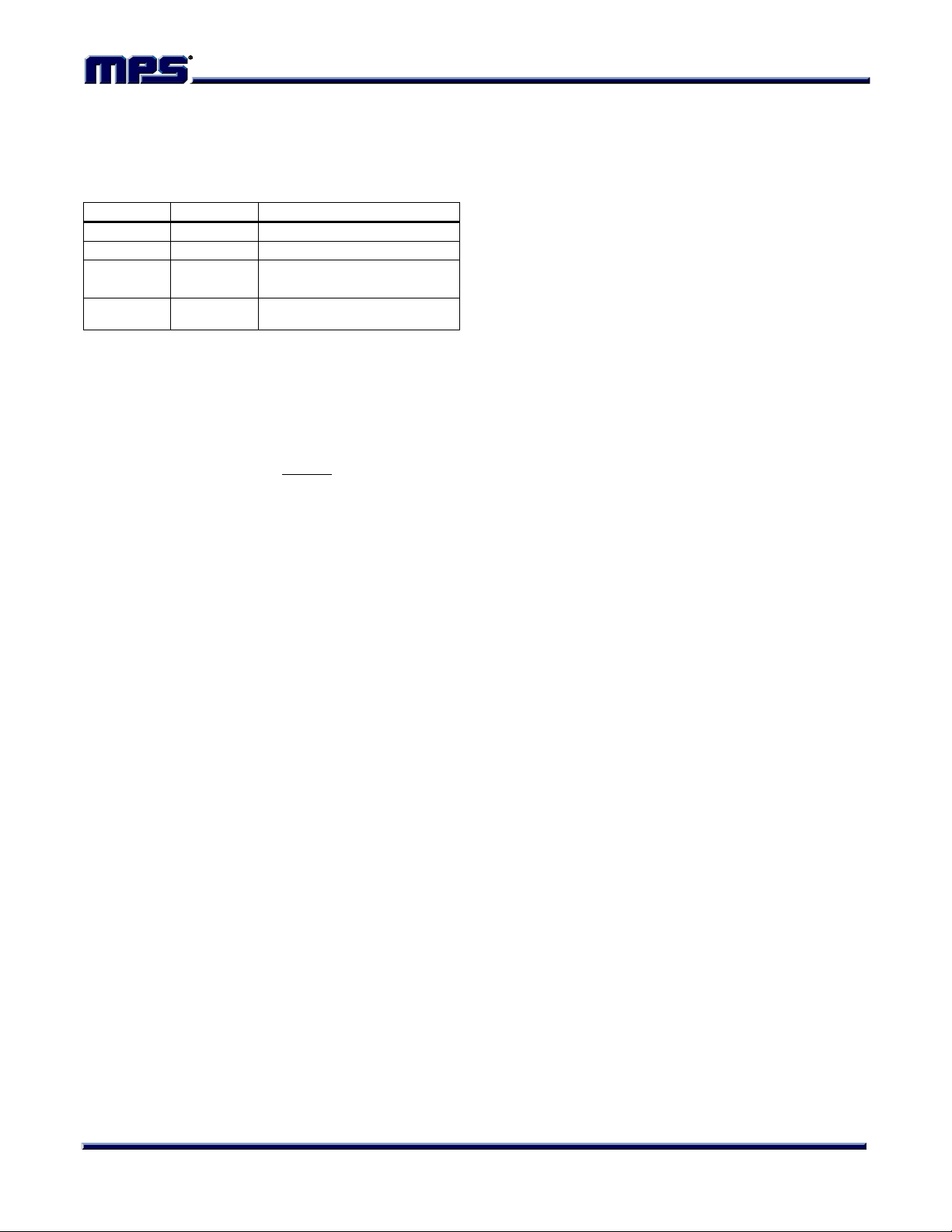
The user can choose to set the input current limit
through the two logic pins M0 and M1 as shown
in Table 1 according to its input specification.
MP2625 Rev. 1.12 www.MonolithicPower.com 15
10/29/2013 MPS Proprietary Information. Patent Protected. Unauthorized Photocopy and Duplication Prohibited.
© 2013 MPS. All Rights Reserved.
Page 16
MP2625 – SINGLE CELL SWITCHING CHARGER WITH POWER PATH CONTROL
M0
M1
Mode
Low
Low
USB2.0 Mode
Low
High
USB3.0 Mode
High
Low
Programmable Mode
High/Float
High/Float
Default Mode
IN_LIM
R1+R2
V =1.52 (V)
R2
When both M0 and M1 are float, they are pulled
to the logic high, under this condition, the input
current is limited to a default value of 2A.
Table 1―Input Current Limit Setting
Input Voltage Limit Setting
The input voltage can be limited at a value set by
a resistor divider from IN pin to VLIM pin to
AGND according to the following expression
(Typical Application Circuit):
When the voltage on VLIM pin drops and hits the
reference voltage 1.52V, the input voltage will be
clamped to the setting value.
the battery charger may or may not be able to
charge at the full programmed rate. The system
load is always satisfied first over the battery
charge current. If the system load requirement is
low, the battery can be charged at full constant
current.
When the battery voltage reaches the battery full
threshold, the charger enters the “constant
voltage mode” operation.
End of Charge (EOC) and Indication
In constant voltage charge mode, the battery
voltage is regulated at 4.2V (when SYSFB is float
or SYS is programmed higher than battery full
threshold) and the charge current decreases
naturally. Once the charge current hits the
battery full threshold IBF (1/10 programmed
charge current), the battery is fully charged and
charge cycle is terminated.
If the charge current drops below IBF because of
any limit condition, the MP2625 will come out of
CV mode, and the charge full detection is invalid.
Battery Charger
The MP2625 completes charge operation consist
of trickle charge, automatic charge termination,
charge status indication, timer control, NTC
indication, automatic recharge, and thermal
limiting.
When the PWM converter is out of soft start, the
battery charge cycle begins, the MP2625 first
determines if the battery is deeply discharged. If
the battery voltage is lower than the trick charge
threshold (typical 3.0V), the battery charger starts
in “trickle charge mode”. The trickle charge
current is limited to 10% of the programmed
charge current until the battery voltage reaches
3.0V. If the charge stays in the “trickle charging
mode” for longer than 45 minutes, the “timer out”
condition is triggered, the charge is terminated
_____________
and CHGOK
will start blinking to indicate that the
battery is unresponsive. When the battery
voltage is above 3.0V, the charger is operating at
“constant current mode.” The current delivered to
the battery will try to reach the value
programmed by the ISET pin. Depending on the
available input power and system load
conditions,
A safe timer starts at the beginning of each new
charge cycle and it monitors if the whole charge
period is within the programmed time limit. After
each charge cycle, when the battery is indicated
as full, the timer counter will be reset. If the time
is expired while the charging is still on going, the
timer will force the MP2625 to terminate charging
_____________
CHGOK
is blinking to indicate the fault condition.
If system voltage is programmed lower than 4.2V
by the resistor divider at the SYSFB pin, the
battery will be charged most close to V
SYS
until
the charge current reaches the IBF threshold.
During charging, the PWM converter continues to
power the system at the same time, if the system
load increases over the input current limit, the
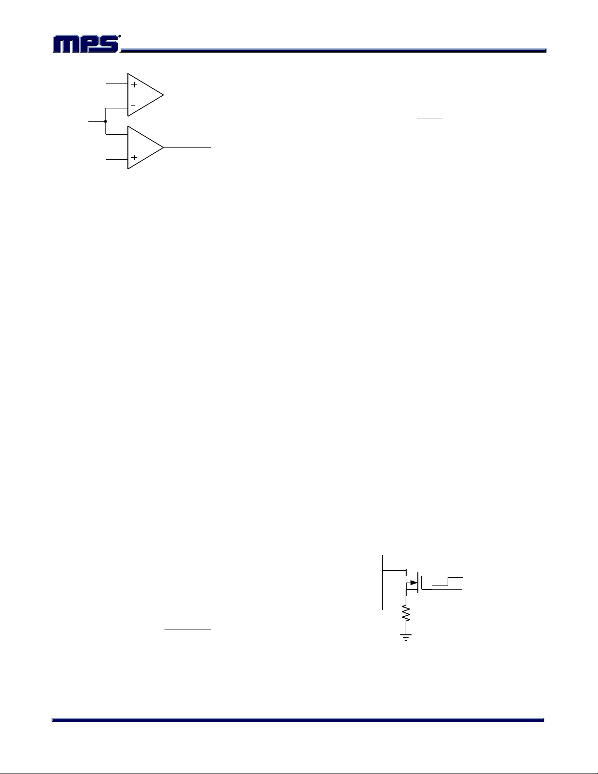
battery charger will change to “ideal diode mode”.
Two comparators between V
used to detect this condition. If V
and V
SYS
SYS<VBATT
are
BATT
-40mV
is triggered, the ideal diode mode is enabled,
else, if V
increases back to V
SYS
SYS>VBATT
+40mV,
the ideal diode mode is disabled as shown in
Figure 3.
MP2625 Rev. 1.12 www.MonolithicPower.com 16
10/29/2013 MPS Proprietary Information. Patent Protected. Unauthorized Photocopy and Duplication Prohibited.
© 2013 MPS. All Rights Reserved.
Page 17
MP2625 – SINGLE CELL SWITCHING CHARGER WITH POWER PATH CONTROL
V
BATT
+40mV
Enable Ideal Diode Mode
V
SYS
Disable Ideal Diode Mode
V
BATT
-40mV
CHG
SET
1800
I 1.15 (mA)
R (k )
CHG
ISET
BATT
I×
1.15
V
=I
ISET
R
ISET
OFF ON
Figure 3— Ideal Diode Mode Enable/Disable
In summary, the terminal battery voltage is 4.2V
(typical) when SYSFB is float or programmed
higher than battery full threshold-4.2V, and V
SYS
IBF40mΩ when SYSFB is connected to the
resistor divider- programmed lower than 4.2V.
can be calculated by monitoring the ISET pin
voltage with the following formula:
Additionally, the actual battery charge current
may be lower than the programmed current due
to limited input power available and prioritization
of the system load.
Battery charge full current threshold IBF is set
internally at 10% of the programmed charge
current. However, IBF has a 150mA maximum
-
limit which can not be exceeded.
Logic Control
Automatic Recharge
Once the battery charge cycle is completed, the
MP2625 turns off indicating the battery full status.
During this process, the battery power may be
consumed by the system load or self discharge.
If the input power is always on, to ensure the
battery not to be exhausted, the new charge
cycle will automatically begin when the battery
voltage falls below the auto-recharge threshold
V
which is typically 4V when the SYSFB is
RCHG
float, and 50mV lower if the SYSFB is connected
to a resistor divider. The timer will re-start when
the auto-recharge cycle begins.
During the charge off state when the battery is
fully charged, if the input power is recycled, or
the EN signal is refreshed, the charge cycle will
re-start and the timer will refresh even if the
battery voltage is above the auto-recharge
threshold.
Charge Current Setting
The charge current of the MP2625 is
programmed using a single resistor from ISET
pin to ground. The program resistor and charge
current are calculated using the following
equations:
The MP2625 has two separate enable control
pins.
_____
EN
is a logic control pin that controls the
operation of the whole IC. When EN
IC is enabled and the PWM converter output
powers the system and the charger. When EN
_____
is low, the
_____
is
high, both the PWM converter and the charger
are disabled. The BATT to SYS switch turns fully
on to connect the battery to power the system.
The ISET pin can be also used to control the
operation of the charger. Setting ISET pin floating
will disable the charger function while the output
of PWM converter will continue supply power to
system. On the other hand, a resistor from ISET
to AGND will enable the charging at the
programmed charge current.
The logic control of the ISET pin of the MP2625
can be realized as Figure 4. In this way, the user
can choose logic low to be “on” signal or logic
high to be ”off” signal with a N-MOSFET.
At either constant current mode or constant
voltage mode, the voltage at the ISET pin is
proportional to the actual charge current
delivered to the battery, I
MP2625 Rev. 1.12 www.MonolithicPower.com 17
10/29/2013 MPS Proprietary Information. Patent Protected. Unauthorized Photocopy and Duplication Prohibited.
© 2013 MPS. All Rights Reserved.
. The charge current
BATT
Figure 4— ISET Logic Control
Page 18
MP2625 – SINGLE CELL SWITCHING CHARGER WITH POWER PATH CONTROL
ACOK
CHGOK
Charger Status
low
low
In charging, supplement
mode
low
high
End of charge, ISET
disable charger only.
low
blinking at
6Hz
NTC fault, timer out
high
high
VIN absent, EN disable,
thermal shutdown
TMR
Trickle_TMR
C
t 45 (min)
0.1μF
CHG
(I 1A)
TMR
Total_TMR
C
t 6.5 (hr)
0.1μF
CHG
(I 1A)
Input Power Status Indication (ACOK
__________
)
An internal under voltage lockout circuit monitors
the input voltage and keeps the IC in off state
until the input rises over the rising threshold
(3.8V). When the input voltage decreases below
threshold (3.5V), the IC will turn off, and the
system load will be powered by the battery
automatically. ACOK
__________
is an open-drain, activelow output that indicates the status of input
power. The input is considered valid when the
input voltage is over the UVLO rising threshold,
and 310mV higher than the battery voltage to
ensure both the converter and the charger can
operate normally. If the input voltage from an
adapter or from a USB port is indicated OK,
__________
ACOK
During EN
the ACOK
will turn low.
_____
__________
off or thermal shutdown conditions,
turns high to indicate no power is
__________
provided by the input to the system. The ACOK
signal indicates if input supplies power to the
system load or not. Any other condition can not
affect the ACOK
__________
indication as long as the input
power is present.
Charge Status Indication (CHGOK
_____________
CHGOK
is an open-drain, active-low output that
indicates the status of charge. CHGOK
_____________
)
_____________
will be
low during normal charging operation, turn high
after charge full, and blink if a fault condition
happens including NTC fault (battery temperature
invalid) and timer out (bad battery).
In the event of a fault condition, CHGOK
_____________
switches at 6Hz with the 50% duty cycle and
enter “blinking” mode. The user should check the
application circuit to find out the root cause of the
fault condition if the “blinking” signal is asserted.
For no battery condition, CHGOK
_____________
is blinking
according to the transition between charging and
charge full. The blinking frequency is determined
by the cycle of charge and discharge of the
output capacitor.
When the charge current to the battery is low or
in the event the battery is in supplement mode
_____________
caused by the insufficient input power, CHGOK
keeps low to avoid providing false charge full
indication.
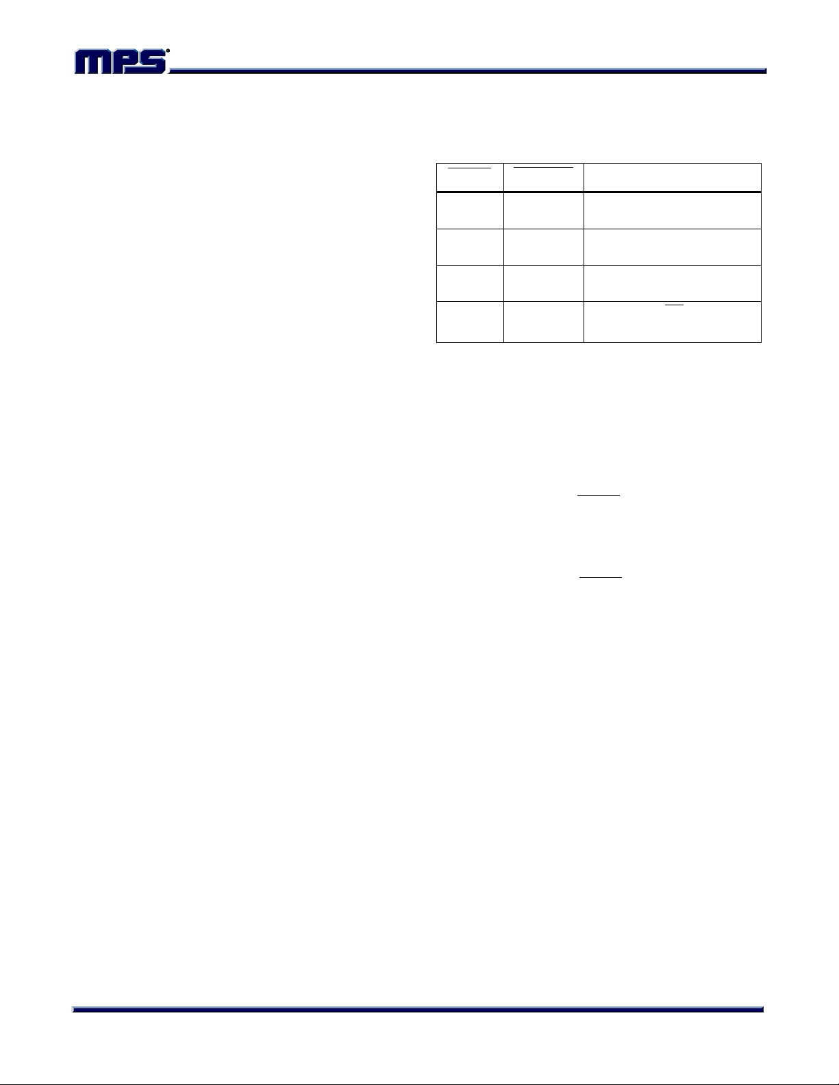
Table 2 shows the ACOK
__________
_____________
and CHGOK
under different charge conditions.
Table 2―Charger Status Indication
Timer Setting
The MP2625 uses an internal timer to terminate
charge if the timer times out. The timer duration
is programmed by an external capacitor at the
TMR pin and related to the real charge current.
The trickle mode charge time is:
The total charge time is:
The above equations are based on 1A charge
current. As a result of power path management
control, charge current might vary during normal
operation, under this condition, the MP2625
automatically takes into account this variation
and adjust the timer period accordingly.
When the charge current is set larger than 1A,
the safe timer period is reduced accordingly with
the same TMR capacitor. If the charge current is
reduced because of insufficient input power, the
timer period is increased proportionally by the
same rate at which the charge current is reduced.
If charge is stopped due to high system load, the
timer is temporarily suspended.
This feature avoids indicating a false trigger
indication for bad battery indication when there is
little charge current delivered to the battery as a
result of the insufficient input power.
status
MP2625 Rev. 1.12 www.MonolithicPower.com 18
10/29/2013 MPS Proprietary Information. Patent Protected. Unauthorized Photocopy and Duplication Prohibited.
© 2013 MPS. All Rights Reserved.
Page 19

MP2625 – SINGLE CELL SWITCHING CHARGER WITH POWER PATH CONTROL
When the timer out condition occurs, the MP2625
_____________
terminates the charge at once and CHGOK
blinks to indicate the fault status. If one of the
following events happens, the timer is refreshed
and MP2625 re-starts the charge cycle.
Input re-startup
Refresh EN
_____
/ISET signal
Auto-Recharge
NTC Thermistor
The NTC pin allows MP2625 to sense the battery
temperature using the Negative Thermal
Coefficient (NTC) thermistor usually available in
the battery pack to ensure safe operating
environment of the battery. A resistor with
appropriate value should be connected from VCC
to NTC and the NTC resistor is from NTC pin to
AGND. The voltage on NTC pin is determined by
the resistor divider whose divide ratio as the
different resistance of the NTC thermistor
depends on the ambient temperature of the
battery.
The MP2625 has an internal NTC voltage
comparator to set the upper and lower limit of the
divide ratio. If NTC pin voltage falls out of this
range it means the temperature is outside the
safe operating range,
As a result, The MP2625 will stop charging and
report it on indication pins. Charging will
automatically resume after the temperature falls
back into the safe range.
Thermal Protection
The MP2625 implements thermal protection to
prevent the thermal damage to the IC or
surrounding components. An internal thermal
sense and feedback loop will automatically
decrease the charge current when the dietemperature rises to about 120oC. This function is
referred as charge current thermal fold-back.
This feature protects the MP2625 from excessive
temperature due to high power operation or high
ambient thermal conditions. Another benefit of
this feature is charge current can be set
according to the requirement rather than worstcase conditions for a given application with the
assurance of safe operation. The MP2625 will
stop charging if the junction temperature rises
above 150oC as the IC enters thermal shutdown
protection.
Ideal Diode Mode
If the system current requirement increases over
the preset limit of the PWM converter, the
additional current will be drawn from the battery
via the BATT-to-SYS switch. To avoid very large
currents being drawn from the battery which
might affect the reliability of the device, the
MP2625 controls the charge switch to work at the
ideal diode mode regulating V
when V
Only when V
is 40mV lower than V
SYS
is 40mV higher than V
SYS
SYS
to V
BATT
BATT
is detected.
charger switch exits the ideal diode mode, and
the charge cycle softly restarts.
Battery Discharge Protection
When the input power is removed or invalid, the
system load will draw power from the battery via
the battery switch. Under this condition, the
battery switch is fully on to minimize the power
loss. The MP2625 integrates battery discharge
protection. If the battery discharge current is
larger than the discharge current limit threshold
I
(3.3A), the current will be regulated at the
DIS
preset limited value. And if the current increases
further, the SYS voltage starts to decrease.
When V
V
, SYS short condition is detected. Under this
BATT
drops to about 800mV lower than
SYS
condition, the discharge current is limited at
200mA. In the event of a short from system to
GND the discharge current from the battery to
the system is also limited to 200mA.
Furthermore, battery voltage UVLO is always
monitored. If the battery voltage is lower than the
battery UVLO threshold, the battery switch is
turned off immediately. This feature makes sure
the battery from over-discharged.
Dynamic Power Path Management (DPPM)
In the presence of a valid input source, the PWM
converter will supply the current to both the
system and the battery charger.
The voltage V
of the battery voltage. When V
3.4V, V
SYS
charge the battery. When V
is regulated based on the value
SYS
is higher than
BATT
is regulated 200mv above V
is lower than
BATT
3.4V, to ensure the system can still be powered
-65mV
BATT
BATT
, the
to
MP2625 Rev. 1.12 www.MonolithicPower.com 19
10/29/2013 MPS Proprietary Information. Patent Protected. Unauthorized Photocopy and Duplication Prohibited.
© 2013 MPS. All Rights Reserved.
Page 20

MP2625 – SINGLE CELL SWITCHING CHARGER WITH POWER PATH CONTROL
up even with a drained battery connected, V
SYS
is
regulated at constant 3.6V.
When the input source is overloaded, either the
current exceeds the input current limit or the
voltage falls below the input voltage limit, the
MP2625 then reduces the charge current until
the input current falls below the input current limit
and the input voltage rises above the input
voltage limit. If the system current increases
beyond the power allowed by the input source,
additional power will be drawn from the battery
via an on-chip 40mΩ MOSFET working as an
ideal diode.
Additionally, if the input source is removed, the
MP2625 will turn on the 40mΩ MOSFET allowing
the battery to power the system load to keep the
operation of the portable device.
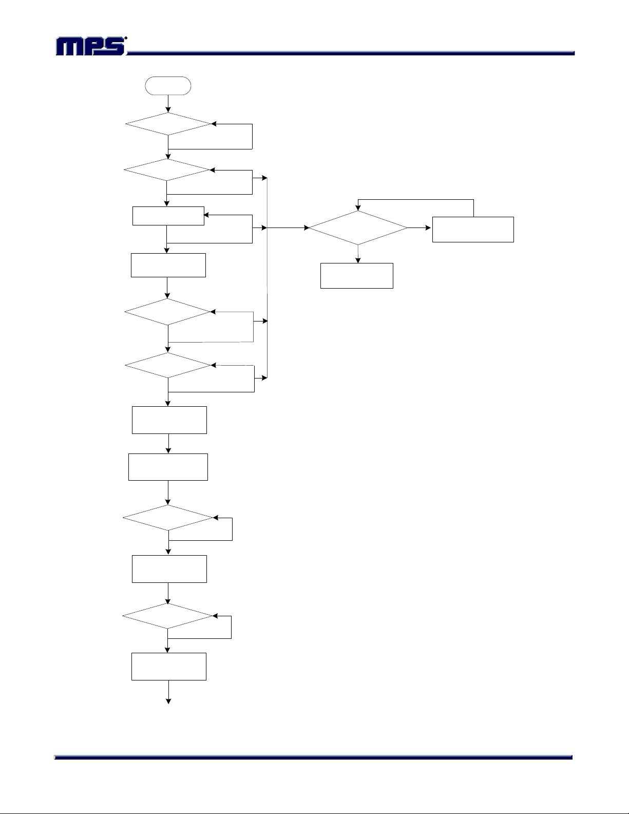
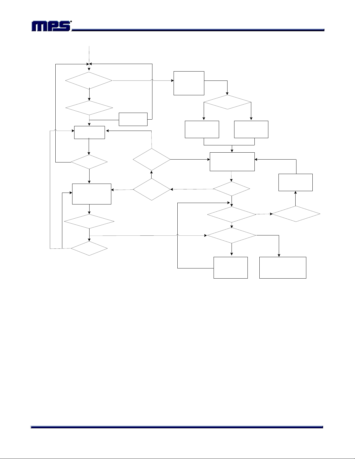
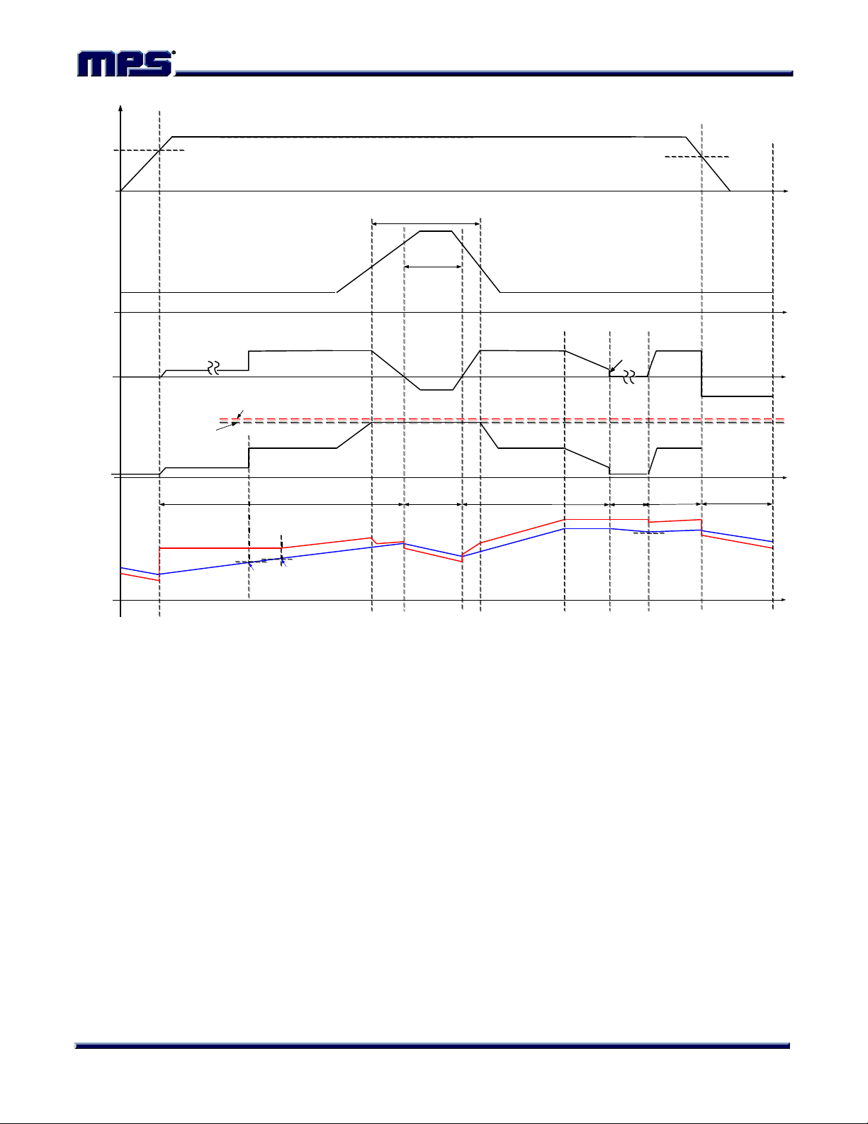
Operation Flow Chart
Figure 5 shows the operation flow chart of the
MP2625.
Figure 6 shows the operation process.
MP2625 Rev. 1.12 www.MonolithicPower.com 20
10/29/2013 MPS Proprietary Information. Patent Protected. Unauthorized Photocopy and Duplication Prohibited.
© 2013 MPS. All Rights Reserved.
Page 21
MP2625 – SINGLE CELL SWITCHING CHARGER WITH POWER PATH CONTROL
VIN>3.0V?
POR
Chip Enable?
No
Enable BG
Yes,
POR="0"
Yes
BGOK="1"
BGOK="0"
No,
POR="1"
Enable VREF LDO
Yes,
UVLO="0"
No,
UVLO="1"
VIN>V
BATT
+310mV ?
Yes
Enable DC-DC
DC-DC soft starts
V
SYS_REF
=max(V
BATT
+
200mV,3.6V)
DC-DC starts ready?
Enable Battery
Charger
V
SYS>VBATT
?
ISET OK?
BATT-to-SYS
switch turns off
Yes
No
Yes
No
V
BATT>VBATT_UVLO
?
Yes
System shuts down
No power to system
Battery power system
Enable discharge limit
No
No
VIN>V
IN_UVLO(VTH
)?
MP2625 Rev. 1.12 www.MonolithicPower.com 21
10/29/2013 MPS Proprietary Information. Patent Protected. Unauthorized Photocopy and Duplication Prohibited.
© 2013 MPS. All Rights Reserved.
Page 22
MP2625 – SINGLE CELL SWITCHING CHARGER WITH POWER PATH CONTROL
Any Limit condition
triggered?
No
Yes
V
BATT
>3.0V?
No
CC/CV Charge
I
CHG=IBF
?
Yes
Charge Full, EOC=1
TMR off,
clear the counter
DC-DC keeps work
V
BATT<VRCHG
?
Yes
V
SYS<VBATT
-40mV?
No
Yes
No
Clamp DC-DC
EAO to regulate
the part
at the limit state
Yes
Trickle Charge
I
CHG
=10%I
CC
V
BATT
<3.4V?
V
SYS
drops down,
Charge switch
is fully on
Yes
Decrease I
CHG
,
Keep V
SYS
=3.6V
No
I
CHG
=0?
Yes
V
SYS<VBATT
-40mV?
Yes
Ideal Diode Mode:
V
SYS=VBATT
-65mV,
Enable discharge
current limit
V
BATT>VBATT_UVLO
?
Yes
V
SYS>VBATT
+40mV?
No
Battery switch shuts down,
DC-DC in over load
condition,
V
SYS
drops down
No
Charge in
CV mode and
I
CHG<IBF
?
No
Yes
No
No
No
Satisfy System current
Charge the battery with
remaining current
Limit condition
Removed?
Yes
No
Yes
Disable
Ideal Diode Mode
Figure 5— MP2625 Operation Flow Chart under No Fault Condition
MP2625 Rev. 1.12 www.MonolithicPower.com 22
10/29/2013 MPS Proprietary Information. Patent Protected. Unauthorized Photocopy and Duplication Prohibited.
© 2013 MPS. All Rights Reserved.
Page 23
MP2625 – SINGLE CELL SWITCHING CHARGER WITH POWER PATH CONTROL
V
IN
Normal
operation
voltage
UVLO
Thresohold
UVLO
Threshold-Hys
0
0
0
I
BATT
V
BATT
0
Power Path Management
I
SYS-IIN_LIM
0
I
IN_AVE
Input Power
Current Limit
CV Charge
Battery
Supplement
Mode
Charging
Supplement
Mode-
Discharging
Charging
Auto-
Recharging
Trickle Charge
CC Charge
Battery
Full
Self-
discharging
V
BATT
=3.0V
V
BATT=3.4V
=4.0V
Power off-
discharging
V
SYS
V
BATT
I
IN_LIM
I
SYS
Figure 6— MP2625 Operation Process under No Fault Condition
MP2625 Rev. 1.12 www.MonolithicPower.com 23
10/29/2013 MPS Proprietary Information. Patent Protected. Unauthorized Photocopy and Duplication Prohibited.
© 2013 MPS. All Rights Reserved.
Page 24
MP2625 – SINGLE CELL SWITCHING CHARGER WITH POWER PATH CONTROL
IN
ILIM
40000
I 1.14 (mA)
R (k )
CHG
SET
1800
I 1.15 (mA)
R (k )
)A(
V
IV
I
TC
ILIMIN
MAX_CC
Ilim
=
1
A
Ilim
=0
.
825
A
3V 4.2V
Battery Voltage
Charge Current
1A
2A
Ilim
=
1
.
44
A
(V)
R2+R1
R2
×V=V
IN_LIMVLIM
(V)
R2
R2+R1
×V=V
VLIMIN_LIM
(V)
V
V-V
×R2=R1
VLIM
VLIMIN_LIM
7R
7R6R
VV
REF_SYSSYS
APPLICATION INFORMATION
COMPONENT SELECTION
Setting the Input Current Limit
Connect a resistor from the ILIM pin to AGND
to program the input current limit for different
input ports. The relationship between the input
current limit and setting resistor is as following:
(1)
Where RILIM is greater than 22.8k, so that IILIM is
not over 2A.
For USB input, the input current limit is set by
the M0 and M1 logic, the setting resistor by
ILIM pin is invalid.
Setting the Charge Current
R
connecting from the ISET pin to AGND
ISET
sets the charge current (ICHG). The relationship
between the charge current and setting resistor
is as following:
(2)
Assume I
=2A, thus: R
CHG
=1.05kΩ.
ISET
Usually in USB mode, the charge current is
always set over the USB input limit specification.
Then the MP2625 regulates the input current
constant at the limitation value. Thus the real
CC charge current is not the setting value, it
varies with different input and battery voltages.
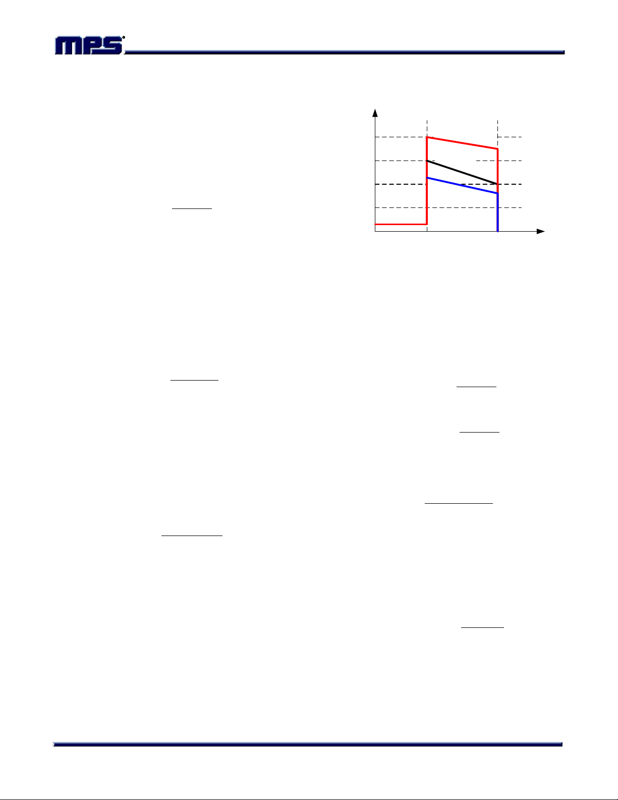
The maximum CC charge value can be
calculated as:
(3)
Where VTC is trickle charge threshold (3V) and η
is the current charge efficiency. Assume
VIN=5.5V, IILIM=1A, η=83%, thus ICC_MAX=1.52A.
Figure 7 shows a calculating charge current
curve by limiting the input current limit.
Figure 7—I
Variation with Different Input
CHG
Current Limit
Setting the Input Voltage Limit
The input clamp voltage is set using a resistive
voltage divider from the input voltage to VLIM
pin. The voltage divider divides the input
voltage down to the limit voltage by the ratio:
(4)
Thus the input voltage is:
(5)
The voltage clamp reference voltage V
VLIM
is
1.52V, and a typical value for R2 can be 10kΩ.
With this value, R1 can be determined by:
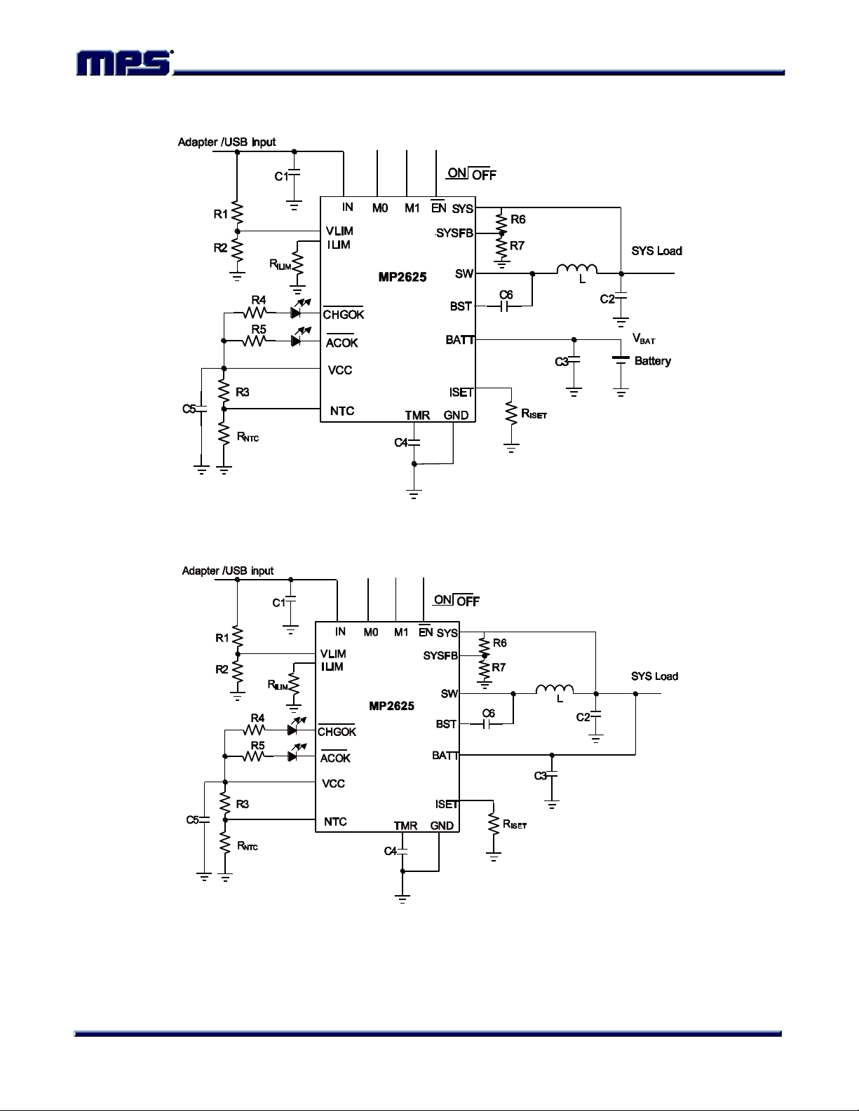
(6)
For example, for a 4.65V input limit voltage, R2
is 10kΩ, and R1 is 20.6kΩ.
Setting the System Voltage
The system voltage can be regulated to any
value between 3.6V to 4.4V by the resistor
divider on SYSFB pin as R6 and R7 in Figure 9.
(7)
MP2625 Rev. 1.12 www.MonolithicPower.com 24
10/29/2013 MPS Proprietary Information. Patent Protected. Unauthorized Photocopy and Duplication Prohibited.
© 2013 MPS. All Rights Reserved.
Where V
SYS_REF
is 1.152V, the reference voltage
of SYS. With a typical value for R7, 10kΩ, R6
can be determined by:
Page 25

MP2625 – SINGLE CELL SWITCHING CHARGER WITH POWER PATH CONTROL
)V(
V
VV
7R6R
REF_SYS
REF_SYSSYS
)MHz(fV
V
I
VV
L
SIN
BATT
MAX_L
BATTIN
)
2
ripple%
1(II
)MAX(LOADPEAK
MAX_IN
TCMAX_INTC
MAX_CCMAX_RMS
V
)VV(V
II
%
Lf2C8
V
V
1
V
V
r
2
S
IN
SYS
SYS
SYS
rLf8
V
V
1
2C
2
S
IN
MIN_SYS
(8)
For example, for a 4.2V system voltage, R7 is
10kΩ, and R6 is 26.5kΩ.
Selecting the Inductor
Inductor selection trades off among cost, size,
and efficiency. A lower inductance value
corresponds to a smaller size, but results in
higher ripple currents, higher magnetic
hysteretic losses, and higher output
capacitances. Choosing a higher inductance
value benefits from lower ripple current and
smaller output filter capacitors, but results in
higher inductor DC resistance (DCR) loss. From
a practical standpoint, the inductor ripple
current does not exceed 30% of the maximum
load current under worst cases conditions. For
the MP2625 operating with a typical 5V input
voltage, the maximum inductor current ripple
occurs at the corner point between trickle
charge and CC charge (VBATT=3V). Estimate the
required inductance as:
(H) (9)
(mA) (10)
capacitors so that the temperature rise due to
the ripple current does not exceed 10°C. Use
ceramic capacitors with X5R or X7R dielectrics
because of their low ESR and small
temperature coefficients. For most applications,
use a 22µF capacitor.
Selecting the Output Capacitor
The output capacitor C2 from the typical
application circuit is in parallel with the SYS
load. C2 absorbs the high-frequency switching
ripple current and smoothes the output voltage.
Its impedance must be much less than that of
the system load to ensure it properly absorbs
the ripple current.
Use a ceramic capacitor because it has lower
ESR and smaller size that allows us to ignore
the ESR of the output capacitor. Thus, the
output voltage ripple is given by:
(12)
In order to guarantee the ±0.5% system voltage
accuracy, the maximum output voltage ripple
must not exceed 0.5% (e.g. 0.1%). The
maximum output voltage ripple occurs at the
minimum system voltage and the maximum
input voltage.
Where VIN, VBATT, and fS are the typical input
voltage, the TC to CC charge threshold, and the
switching frequency, respectively. ΔI
L_MAX
is the
maximum inductor ripple current, which is
usually 30% of the CC charge current.
For ICHG=2A, VIN=5V, VBATT=3V and fs=1.6MHz,
the calculated inductance is 1.3µH. The
maximum inductor peak current exceeds 2.3A.
To optimize efficiency, chose an inductor with a
DC resistance less than 50mΩ. Choose the
inductor 7447745012 from Wurth with ratings at
L=1.2µH/4.6A /21mΩ.
Selecting the Input Capacitor
The input capacitor C1 from the typical
application circuit absorbs the maximum ripple
current from the PWM converter, which is given
by
(A) (11)
For ICC_MAX=2A, VTC=3V, VIN_MAX=14V, the
maximum ripple current is 1A. Select the input
For VIN=14V, V
SYS_MIN
=3.6V, L=1.2µH,
fS=1.6MHz, r =0.1%, the output capacitor can
be calculated as:
(13)
We can then choose a 22µF ceramic capacitor.
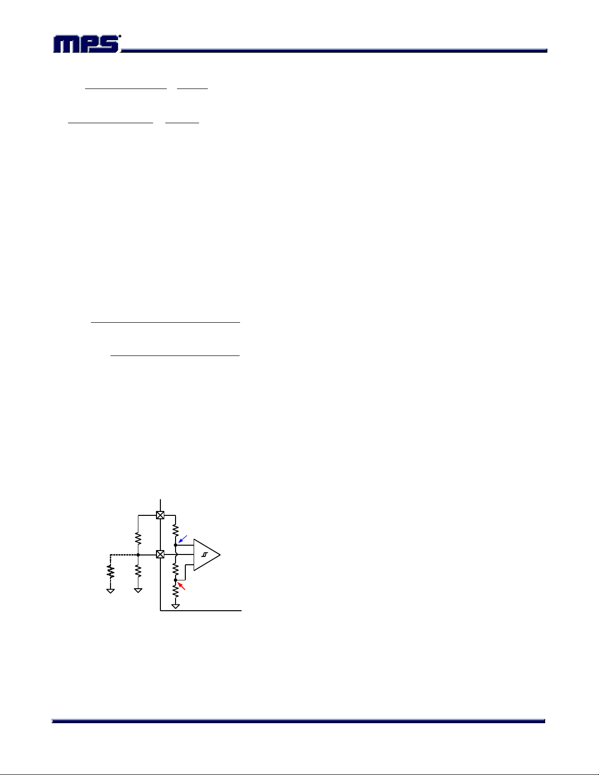
Resistor Choose for NTC Sensor
Figure 8 shows an internal resistor divider
reference circuit to limit the low temperature
threshold and high temperature threshold at
65%·VCC and 33.5%·VCC, respectively. For a
given NTC thermistor, select appropriate RT1
and RT2 to set the NTC window.
MP2625 Rev. 1.12 www.MonolithicPower.com 25
10/29/2013 MPS Proprietary Information. Patent Protected. Unauthorized Photocopy and Duplication Prohibited.
© 2013 MPS. All Rights Reserved.
Page 26
MP2625 – SINGLE CELL SWITCHING CHARGER WITH POWER PATH CONTROL
%65=
VCC
V
=
//RR+R
//RR
TH_Low
NTC_ColdT2T1
NTC_ColdT2
33.5%=
VCC
V
=
//RR+R
//RR
TH_High
NTC_HotT2T1
NTC_HotT2
NTC_HotNTC_Cold
NTC_HotNTC_Cold
T2
R.42250-R1225.0
RR.30
R
)RR(2275.0
RR0.3
R
NTC_HotNTC_Cold
NTC_ColdNTC_Hot
T1
NTC
VCC
Low Temp Threshold
High Temp Threshold
R
NTC
R
T1
R
T2
V
TH_Low
V
TH_High
(14)
(15)
R
is the value of the NTC resistor at high
NTC_Hot
temperature of the required temperature
operation range, and R
NTC_Cold
is the value of
the NTC resistor at low temperature.
The two resistors, RT1 and RT2, allow the high
temperature limit and low temperature limit to
be programmed independently. With this
feature, the MP2625 can fit most type of NTC
resistor and different temperature operation
range requirements.
RT1 and RT2 values depend on the type of the
NTC resistor:
(16)
(17)
For example, for the thermistor NCP18XH103,
it has the following electrical characteristic:
PCB Layout Guideline
It is important to pay special attention to the
PCB layout to meet specified noise, efficiency
and stability requirements. The following design
considerations can improve circuit performance:
1) Route the power stage adjacent to their
grounds. Aim to minimize the high-side
switching node (SW, inductor), trace lengths in
the high-current paths and the current sense
resistor trace.
Keep the switching node short and away from
all small control signals, especially the feedback
network.
Place the input capacitor as close as possible
to the IN and PGND pins.
Place the output inductor close to the IC and
connect the output capacitor between the
inductor and PGND of the IC.
2) For high-current applications, the balls for the
power pads (IN, SW, SYS, BATT and PGND)
should be connected to as much copper in the
board as possible. This improves thermal
performance because the board conducts heat
away from the IC.
At 0°C, R
NTC_Cold
At 50°C, R
The following equations are derived assuming
that the NTC window is between 0°C and 50°C.
According to the above equations to calculate
RT1=6.47kΩ and RT2=21.35kΩ.
= 27.445kΩ;
= 4.1601kΩ.
NTC_Hot
3) The PCB should have a ground plane
connected directly to the return of all
components through vias (two vias per
capacitor for power-stage capacitors, one via
per capacitor for small-signal components). It is
also recommended to put vias inside the PGND
pads for the IC, if possible. A star ground
design approach is typically used to keep circuit
block currents isolated (high-power/low-power
small-signal) which reduces noise-coupling and
ground-bounce issues. A single ground plane
for this design gives good results. With this
small layout and a single ground plane, there is
no ground-bounce issue, and having the
components segregated minimizes coupling
between signals.
Figure 8—NTC Function Block
MP2625 Rev. 1.12 www.MonolithicPower.com 26
10/29/2013 MPS Proprietary Information. Patent Protected. Unauthorized Photocopy and Duplication Prohibited.
© 2013 MPS. All Rights Reserved.
Page 27
MP2625 – SINGLE CELL SWITCHING CHARGER WITH POWER PATH CONTROL
TYPICAL APPLICATION CIRCUITS
Figure 9—Typical Charge Application Circuit with V
Programmed by SYSFB Pin
SYS
Figure 10—Application with Charger Disabled under No Battery Condition
MP2625 Rev. 1.12 www.MonolithicPower.com 27
10/29/2013 MPS Proprietary Information. Patent Protected. Unauthorized Photocopy and Duplication Prohibited.
© 2013 MPS. All Rights Reserved.
Page 28
MP2625 – SINGLE CELL SWITCHING CHARGER WITH POWER PATH CONTROL
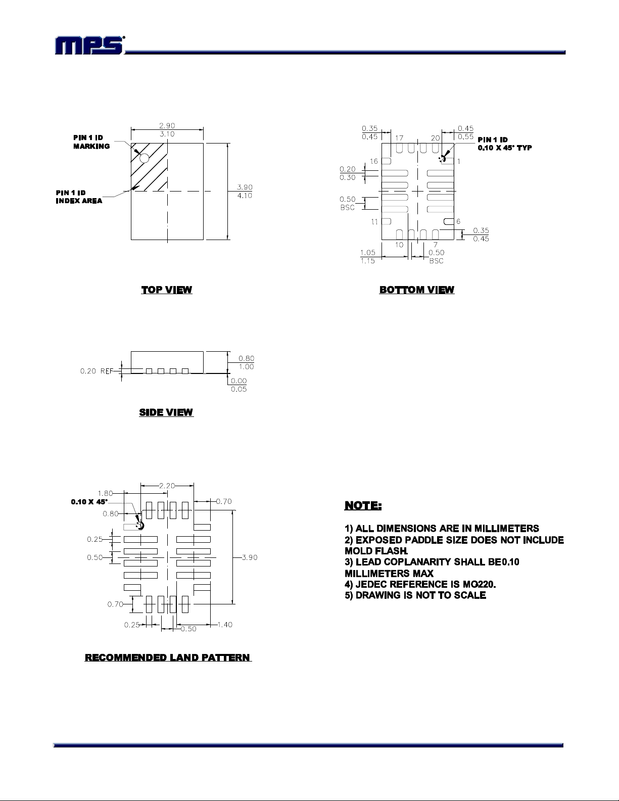
PACKAGE INFORMATION
QFN20-3X4mm
NOTICE: The information in this document is subject to change without notice. Users should warrant and guarantee that third
party Intellectual Property rights are not infringed upon when integrating MPS products into any application. MPS will not
assume any legal responsibility for any said applications.
MP2625 Rev. 1.12 www.MonolithicPower.com 28
10/29/2013 MPS Proprietary Information. Patent Protected. Unauthorized Photocopy and Duplication Prohibited.
© 2013 MPS. All Rights Reserved.
Page 29

 Loading...