

Page 1

Working Instruction /Electrical
Working Instruction, Electrical
Applicable for W760
CONTENTS
1 Read this first!........................................................................................2
2 Lead-free soldering................................................................................3
3 BGA equipment reflow profiles.............................................................5
3.1 General.................................................................................................. 5
3.2 Temperature Measurements ................................................................. 5
3.3 Reflow Profiles ...................................................................................... 6
4 Replacement of components ................................................................7
4.1 D2404: IC IF 3.5X3.5X0.8 ..................................................................... 7
4.2 N1400: Module Bluetooth + FM STLC2592 .......................................... 8
4.3 N1200: RF-Module Thor Pre-bumped................................................... 9
4.4 N1200: RF-Module Thor Pre-bumped Continued ............................. 10
4.5 N1210: RF-Module Mammoth Pre-bumped ........................................11
4.6 N1210: RF-Module Mammoth Pre-bumped Continued..................... 12
4.7 X2200: Battery Connector ................................................................... 13
4.8 X2400: System Connector .................................................................. 14
5 Revision History...................................................................................16
1211-1562 Rev 2 1211-1562
© Sony Ericsson Mobile Communications AB
Page 2

Working Instruction/ Electrical
1 Read this first!
CAUTION
Before you start replacing any components, make sure you have read and fully understood the
contents of section 2 and 3!
Use Electrostatic Discharge (ESD) equipment to avoid damaging the PBA.
Use gloves or finger cots to avoid contaminating the PBA with skin oil.
EQUIPMENT
For equipment information, refer to the Electrical and Mechanical Equipment Lists.
MECHANICAL INSTRUCTIONS
For phone disassembly and reassembly information, refer to the Mechanical Working
Instruction.
1211-1562 Rev 2 2(16)
© Sony Ericsson Mobile Communications AB
Page 3
Working Instruction/ Electrical
2 Lead-free soldering
THIS PRODUCT IS MANUFACTURED WITH LEAD-FREE SOLDER
AND LEAD
During electrical repair, it is critical to make sure that no lead is
introduced.
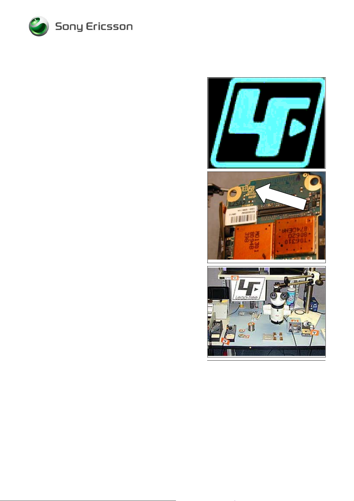
This symbol indicates that the product is lead- free.
-FREE COMPONENTS!
The lead-free symbol is located on the PCB as shown.
A lead-free work area must be set up completely separated
from work areas that are used to make lead repairs. The leadfree work area must also be clearly labeled with the lead free
symbol as shown in the adjacent picture. The items on this
desk must remain lead-free. They must be adequately labeled
to make their lead-free status clearly and easily recognized.
1211-1562 Rev 2 3(16)
© Sony Ericsson Mobile Communications AB
Page 4
Working Instruction/ Electrical
Lead-free soldering continued
LFS (lead-free solder) characteristics:
• High melting point (typically 217°C)
• Low wetting
• High surface tension
• Difficult to spread
• Recommended tip temperature = 370°C
WHEN SERVICING PBAS THAT HAVE BEEN MANUFACTURED
LFS (LEAD-FREE SOLDER), LFS MUST BE USED!
WITH
F NOT, THERE IS A HIGH RISK OF UNRELIABLE SOLDERING
I
JOINTS
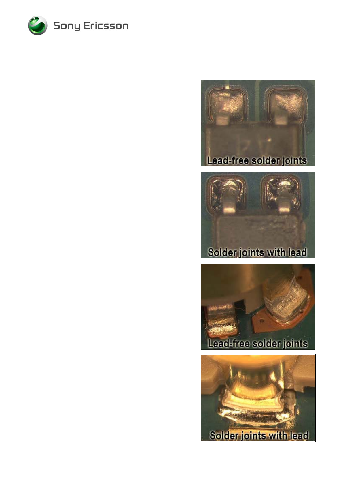
Lead-free solder joints are more difficult to inspect because they
do not have shiny surfaces like leaded solder joints. Also, leadfree solder does not flow as well as leaded solder, so some of
the solder pad areas may remain exposed.
!
1211-1562 Rev 2 4(16)
© Sony Ericsson Mobile Communications AB
Page 5

Working Instruction/ Electrical
3 BGA equipment reflow profiles
3.1 General
This section contains reflow profile recommendations for mobile phones and similar products.
They are just general recommendations and considerations have to be taken for every single product.
The solder is secondary but could also affect the parameters.
In this document one alloy is specified: SnAgCu (Lead free) melting point 217°C
3.2 Temperature Measurements
At least four probes should be used.
They should be placed on components with the highest and lowest thermal mass.
The probes shall be located in the beginning, in the middle, and at the end of the board/panel.
It is recommended that the probes are soldered on the board, but glue and Kapton tape can be used.
At least one probe shall be placed in the air or on top of a component.
These values are strongly dependent on the BGA replacement equipment.
Select a nozzle size that is the same size or slightly larger than the part being replaced.
Make sure the nozzle does not affect any nearby placed components.
T
HESE VALUES ARE RECOMMENDATIONS AND MAY HAVE TO BE CHANGED DEPENDING ON THE TYPE OF
EQUIPMENT
HE MAXIMUM TEMPERATURE FOR ANY COMPONENT MUST NOT EX CEED 260°C!
T
!
1211-1562 Rev 2 5(16)
© Sony Ericsson Mobile Communications AB
Page 6

Working Instruction/ Electrical
3.3 Reflow Profiles
Sn/Ag/Cu (lead-free)
Ramp rate < 4°C/sec
Ramp rate cooling zone < 6°C/sec
Time above liquidus 60-150 sec
Minimum temperature 235°C
Maximum temperature 245°C or 260°C for 10 sec. (the higher
temperature in case the board has
extremely high ΔT)
Bottom heat temperature 125°C-150°C
Total time Approx. 4-7 min
1211-1562 Rev 2 6(16)
© Sony Ericsson Mobile Communications AB
Page 7

Working Instruction/ Electrical
4 Replacement of components
4.1 D2404: IC IF 3.5X3.5X0.8
Locate the small, round, tabs around the perimeter of shield
E1000.
Use a dental pick to pry the lid up at each of the tabs. Be
careful to not damage the lid.
Use clippers to trim the overhang as shown.
Make sure the remaining fence metal does not touch parts
on the board, and make sure the metal does not prevent the
lid from assembling properly.
1211-1562 Rev 2 7(16)
© Sony Ericsson Mobile Communications AB
Page 8

Working Instruction/ Electrical
4.2 N1400: Module Bluetooth + FM STLC2592
After removing the lid of shield E1000 as shown in the
D2404 section, cut the crossbar as shown.
Remove the cut section and discard it.
1211-1562 Rev 2 8(16)
© Sony Ericsson Mobile Communications AB
Page 9

Working Instruction/ Electrical
4.3 N1200: RF-Module Thor Pre-bumped
Remove yellow tape from N1200 and N1210.
Apply heat-resistant tape to X4200, X1501, and X2200.
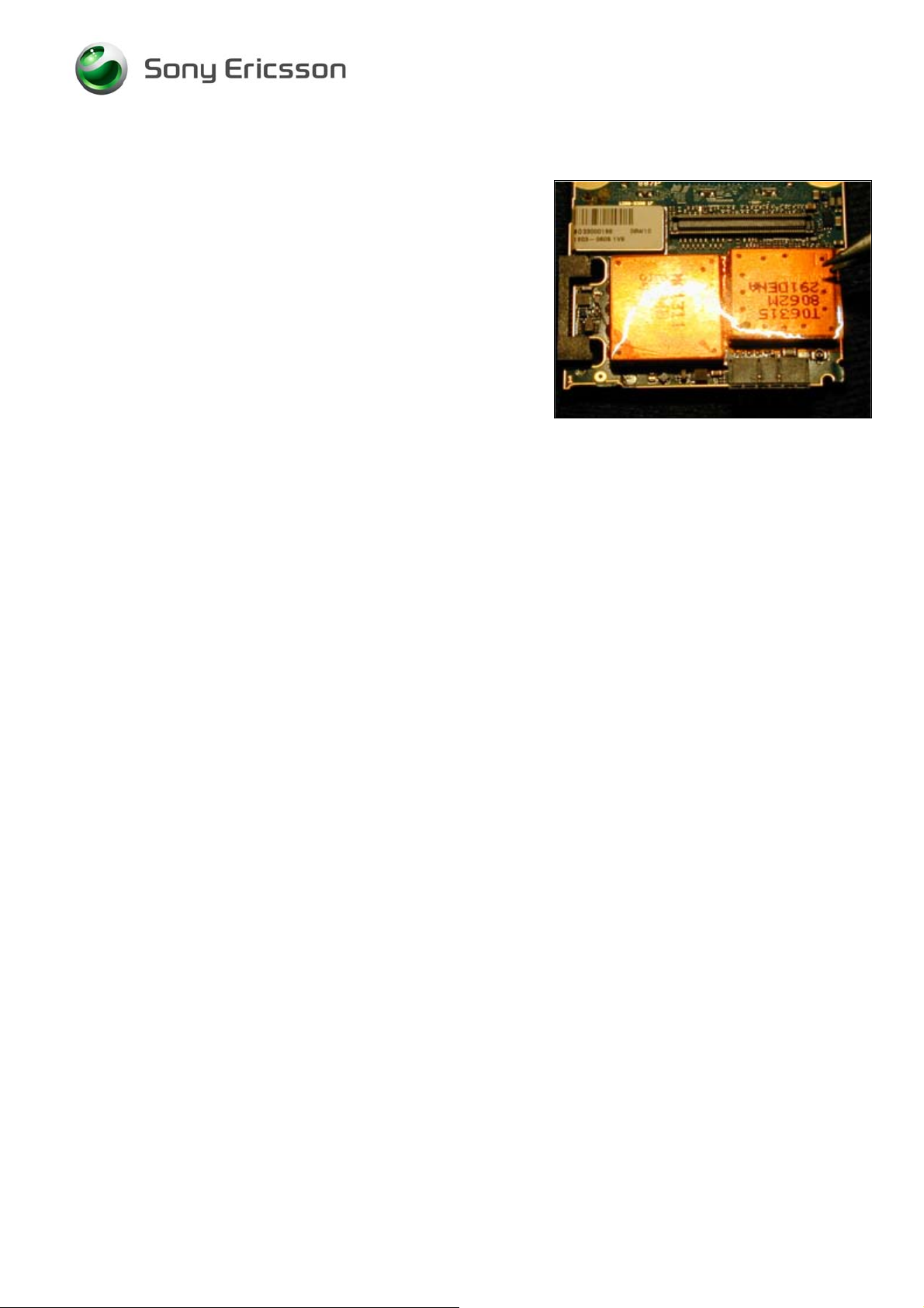
Use a Large Hot Air Device to melt the solder.
Slide the part off the board while the solder is hot.
1211-1562 Rev 2 9(16)
© Sony Ericsson Mobile Communications AB
Page 10

Working Instruction/ Electrical
4.4 N1200: RF-Module Thor Pre-bumped Continued
After installing the new part, apply a new piece of tape to
N1200 and N1210.
1211-1562 Rev 2 10(16)
© Sony Ericsson Mobile Communications AB
Page 11

Working Instruction/ Electrical
4.5 N1210: RF-Module Mammoth Pre-bumped
Remove yellow tape from N1200 and N1210.
Apply heat-resistant tape to X2200 and X2400.
Use a Large Hot Air Device to melt the solder.
Insert tweezers from the left side of the part. Slide the part
toward N1200 and lift it off the board.
1
1211-1562 Rev 2 11(16)
2
© Sony Ericsson Mobile Communications AB
Page 12
Working Instruction/ Electrical
4.6 N1210: RF-Module Mammoth Pre-bumped Continued
After installing the new part, apply a new piece of tape to
N1200 and N1210.
1211-1562 Rev 2 12(16)
© Sony Ericsson Mobile Communications AB
Page 13

Working Instruction/ Electrical
4.7 X2200: Battery Connector
Use heat-resistant tape to protect X1200.
Use a Large Hot Air Device to melt the solder.
Remove the excess solder from the holes.
Insert a new part and solder the pins in the holes.
1211-1562 Rev 2 13(16)
© Sony Ericsson Mobile Communications AB
Page 14
Working Instruction/ Electrical
4.8 X2400: System Connector
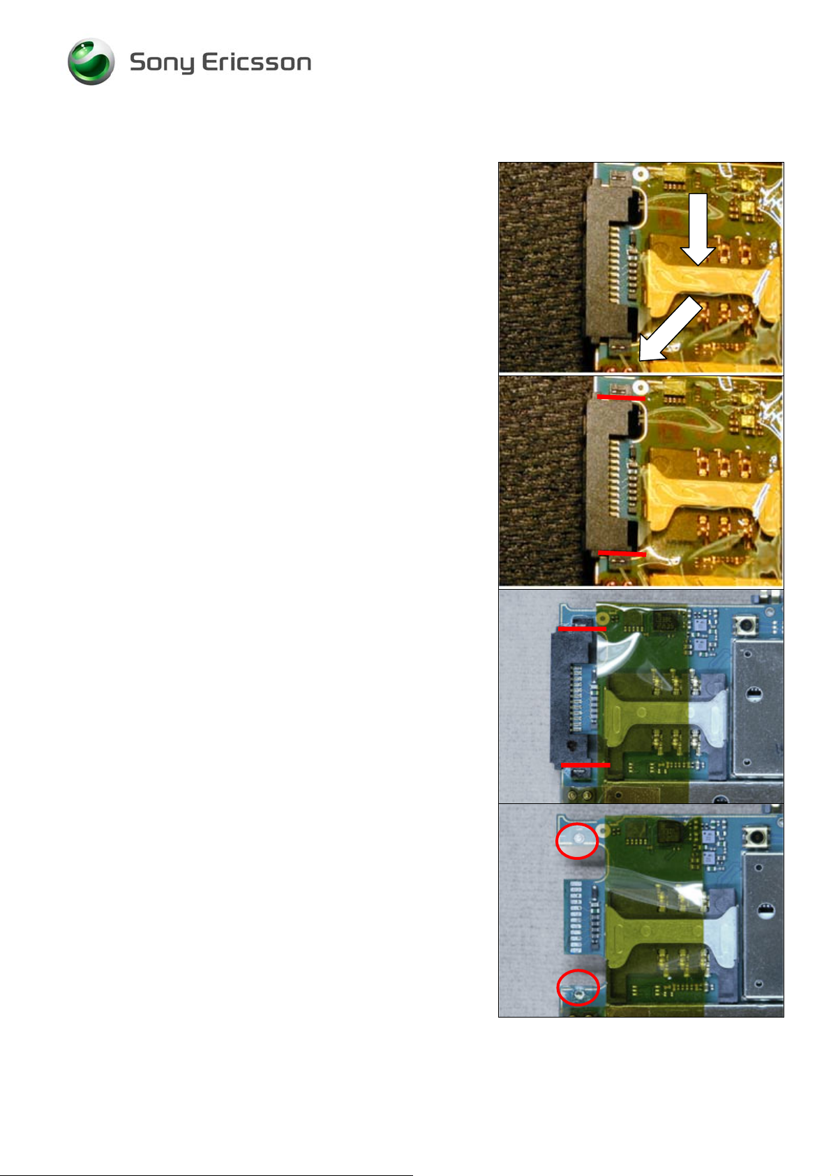
Apply heat-resistant tape to X2410, X1503, and X4100 (not
shown).
CAREFUL NOT TO DAMAGE THE PCB WHEN CUTTING THE
SYSTEM CONNECTOR
Cut the system connector with a cutting pliers as shown by
red line in picture
Use hot air to remove the connector
NOTE: UNDERFILL IS ADDED ON PHONES PRODUCED AFTER
838
W
Use hot air and a dentist hook to remove the underfill
located as shown in pictures.
1211-1562 Rev 2 14(16)
© Sony Ericsson Mobile Communications AB
Page 15

Working Instruction/ Electrical
X2400: System Connector Continued
Remove excess solder from holes and pads.
Use BGA equipment and soldering paste to mount the new
connector.
1211-1562 Rev 2 15(16)
© Sony Ericsson Mobile Communications AB
Page 16

Working Instruction/ Electrical
5 Revision History
Rev. Date Changes / Comments
1 2008-May-26 Initial Release
2 2008-12-09 X2400 System Connector: Method changed
1211-1562 Rev 2 16(16)
© Sony Ericsson Mobile Communications AB
 Loading...