

Page 1
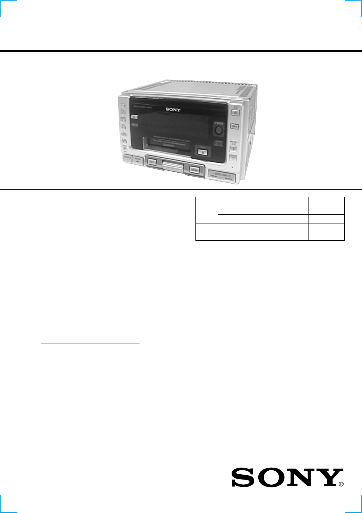
WX-C5000
SERVICE MANUAL
Dolby noise reduction manufactured under license from Dolby Laboratories Licensing Corporation.
“DOLBY” and the double-D symbol ; are trademarks of Dolby
Laboratories Licensing Corporation.
CD
Section
TC
Section
E Model
Model Name Using Similar Mechanism WX-C55
CD Drive Mechanism Type MG-378X-121
Optical Pick-up Name KSS-521A
Model Name Using Similar Mechanism WX-C55
Tape Transport Mechanism Type MG-25E-136
CD player section
Signal-to-noise ratio 94 dB
Frequency response 5 – 20,000 Hz
Wow and flutter Below measurable limit
Cassette player section
Tape track 4-track 2-channel stereo
Wow and flutter 0.08 % (WRMS)
Frequency response 30 – 20,000 Hz
Signal-to-noise ratio
Cassette type Dolby B NR Dolby NR off
TYPE II, IV 67 dB 58 dB
TYPE I 64 dB 55 dB
SPECIFICATIONS
Tuner section
FM
Tuning range FM tuning interval:
50 kHz/200 kHz switchable
87.5 – 108.0 MHz
(at 50 kHz step)
87.5 – 107.9 MHz
(at 200 kHz step)
Aerial terminal External aerial connector
Intermediate frequency 10.7 MHz
Usable sensitivity 9 dBf
Selectivity 75 dB at 400 kHz
Signal-to-noise ratio 65 dB (stereo),
68 dB (mono)
Harmonic distortion at 1 kHz
0.7% (stereo),
0.4% (mono)
Separation 35 dB at 1 kHz
Frequency response 30 – 15,000 Hz
– Continued on next page –
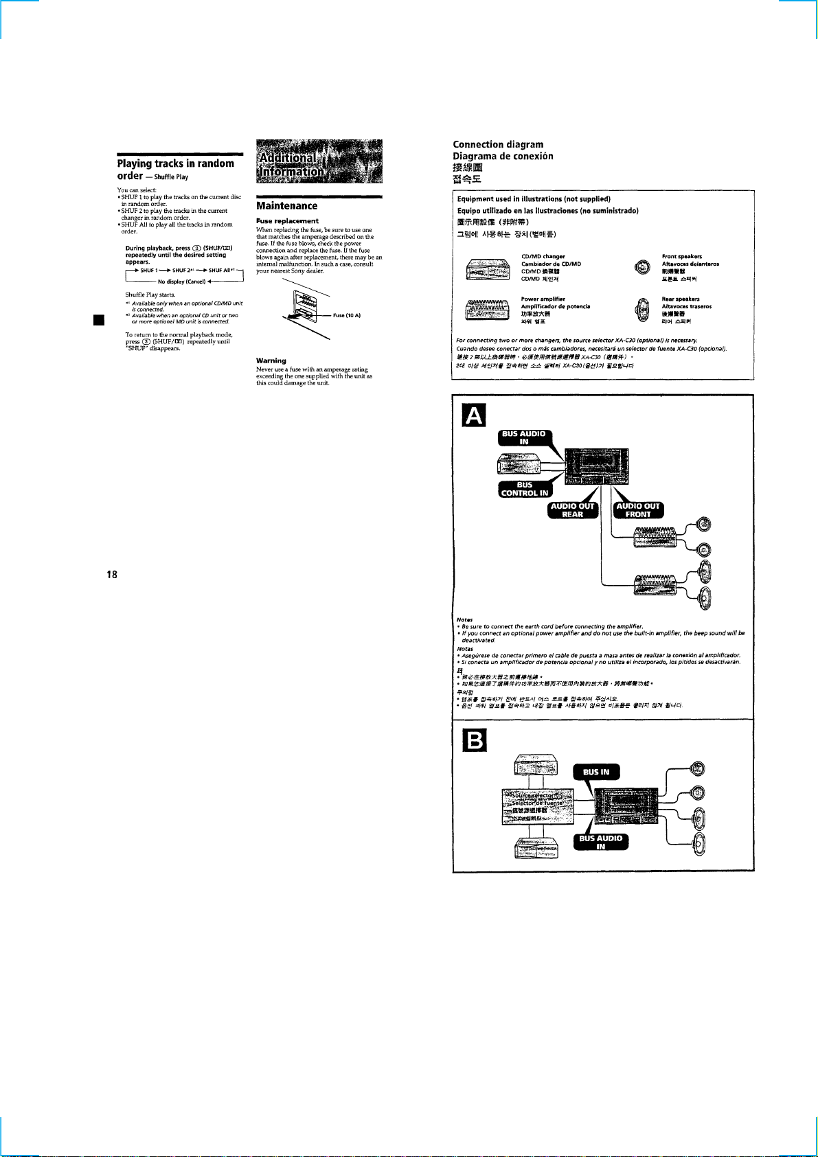
CHANGER CONTROL AUDIO MASTER
1
Page 2

AM
Tuning range AM tuning interval:
9 kHz/10 kHz switchable
531 - 1,602 kHz
(at 9 kHz step)
530 – 1,710 kHz
(at 10 kHz step)
Aerial terminal External aerial connector
Intermediate frequency 10.71 MHz/450 kHz
Sensitivity 30 µV
Power amplifier section
Outputs Speaker outputs
(sure seal connectors)
Speaker impedance 4 – 8 ohms
Maximum power output 45 W × 4 (at 4 ohms)
SERVICE NOTE
CAUTION
Use of controls or adjustments or performance of procedures other than those specified herein may result in hazardous radiation exposure.
Notes on Chip Component Replacement
• Never reuse a disconnected chip component.
• Notice that the minus side of a tantalum capacitor may be dam-
aged by heat.
General
Outputs Audio outputs (2)
Power aerial relay
control lead
Power amplifier control
lead
Intputs Telephone ATT control
lead
Illumination control lead
Bus audio input connector
Bus control input
Power requirements 12 V DC car battery
(negative ground)
Dimensions Approx. 178 × 100 × 181 mm
(w/h/d)
Mounting dimension Approx. 178 × 100 × 160 mm
(w/h/d)
Mass Approx. 2.2 kg
Supplied accessories Parts for installation and
connections (1 set)
Dummy cover (1)
Design and specifications are subject to change without
notice.
NOTES ON HANDLING THE OPTICAL PICK-UP BLOCK
OR BASE UNIT
The laser diode in the optical pick-up block may suffer electrostatic
breakdown because of the potential difference generated by the
charged electrostatic load, etc. on clothing and the human body.
During repair, pay attention to electrostatic breakdown and also use
the procedure in the printed matter which is included in the repair
parts.
The flexible board is easily damaged and should be handled with
care.
NOTES ON LASER DIODE EMISSION CHECK
The laser beam on this model is concentrated so as to be focused on
the disc reflective surface by the objective lens in the optical pickup block. Therefore, when checking the laser diode emission, observe from more than 30 cm away from the objective lens.
NOTES ON PICK-UP FLEXIBLE BOARD
The pick-up flexible board in this set is secured to the optical pickup with an adhesive tape. Once the tape is removed, an adhering
force becomes weak, and it cannot be reused.
Therefore, if the optical pick-up is replaced, replace also the pickup flexible board with a new one.
SAFETY-RELATED COMPONENT WARNING!!
COMPONENTS IDENTIFIED BY MARK 0 OR DOTTED LINE
WITH MARK 0 ON THE SCHEMATIC DIAGRAMS AND IN
THE PARTS LIST ARE CRITICAL TO SAFE OPERATION.
REPLACE THESE COMPONENTS WITH SONY PARTS WHOSE
P ART NUMBERS APPEAR AS SHOWN IN THIS MANU AL OR
IN SUPPLEMENTS PUBLISHED BY SONY.
2
Page 3

TABLE OF CONTENTS
1. GENERAL
Location of Controls............................................................... 4
Getting Started........................................................................ 4
CD Player ............................................................................... 4
Cassette Player ....................................................................... 5
Radio ...................................................................................... 5
Other Functions ...................................................................... 5
CD/MD Unit ........................................................................... 6
Additional Information ........................................................... 7
Connections ............................................................................ 8
2. DISASSEMBLY
2-1. Cover ................................................................................ 10
2-2. Front Panel Assy .............................................................. 10
2-3. CD Mechanism Block ...................................................... 11
2-4. TR Board, Heat Sink ........................................................ 11
2-5. CD Board ......................................................................... 12
2-6. Chassis (U) ....................................................................... 12
2-7. Tape Mechanism Block .................................................... 13
2-8. Main Board ...................................................................... 13
2-9. Chassis (TM) Assy ........................................................... 14
2-10. Sensor Board .................................................................... 14
2-11. Servo Board...................................................................... 15
2-12. Roller Assy....................................................................... 15
2-13. Chassis (OP) (O/S) Assy .................................................. 16
2-14. Optical Pick-up Block ...................................................... 16
3. ASSEMBLY OF MECHANISM DECK
3-1. Housing ............................................................................ 17
3-2. Arm (Suction)................................................................... 17
3-3. Lever (LDG-A)/(LDG-B) ................................................ 18
3-4. Gear (Loading FT) ........................................................... 18
3-5. Guide (C).......................................................................... 19
3-6. Capstan/Reel Motor (M904) ............................................ 19
4. MECHANICAL ADJUSTMENTS.............................. 20
5. ELECTRICAL ADJUSTMENTS
Tape Section ......................................................................... 21
Tuner Section........................................................................ 21
CD Section ........................................................................... 24
6. DIAGRAMS
6-1. IC Pin Descriptions .......................................................... 25
6-2. Block Diagram –CD Section–.......................................... 29
6-3. Block Diagram –Tape Section– ....................................... 30
6-4. Block Diagram –Main Section–....................................... 31
6-5. Circuit Boards Location ................................................... 32
6-6. Printed Wiring Boards –CD Mechanism Section–........... 33
6-7. Schematic Diagram –CD Mechanism Section (1/2)– ...... 34
6-8. Schematic Diagram –CD Mechanism Section (2/2)– ...... 35
6-9. Printed Wiring Board –TR Section– ................................ 36
6-10. Schematic Diagram –TR Section– ................................... 36
6-11. Printed Wiring Board –CD Section–................................ 36
6-12. Schematic Diagram –CD Section–................................... 37
6-13. Printed Wiring Board –Main Section– ............................. 38
6-14. Schematic Diagram –Main Section (1/4)– ....................... 40
6-15. Schematic Diagram –Main Section (2/4)– ....................... 41
6-16. Schematic Diagram –Main Section (3/4)– ....................... 42
6-17. Schematic Diagram –Main Section (4/4)– ....................... 43
6-18. Printed Wiring Board –Control Section– ......................... 44
6-19. Schematic Diagram –Control Section– ............................ 46
6-20. Printed Wiring Board –Jog Section–................................ 47
6-21. Schematic Diagram –Jog Section–................................... 47
7. EXPLODED VIEWS
7-1. Cover Section ................................................................... 53
7-2. Front Panel Section .......................................................... 54
7-3. Chassis Section ................................................................ 55
7-4. Tape Mechanism Section ................................................. 56
7-5. CD Mechanism Section (1) .............................................. 57
7-6. CD Mechanism Section (2) .............................................. 58
7-7. CD Mechanism Section (3) .............................................. 59
8. ELECTRICAL PARTS LIST ................................... 60
3
Page 4
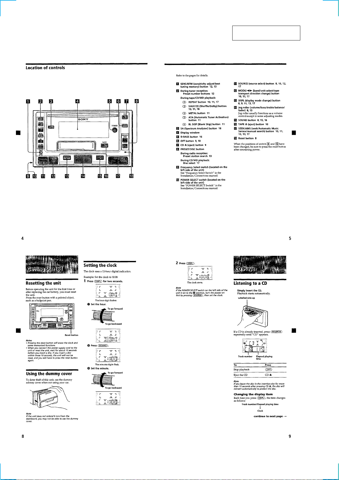
SECTION 1
GENERAL
This section extracted from
instruction manual.
4
Page 5
56789
Page 6
Page 7
Page 8
Page 9
Page 10
SECTION 2
DISASSEMBLY
Note : Follow the disassembly procedure in the numerical order given.
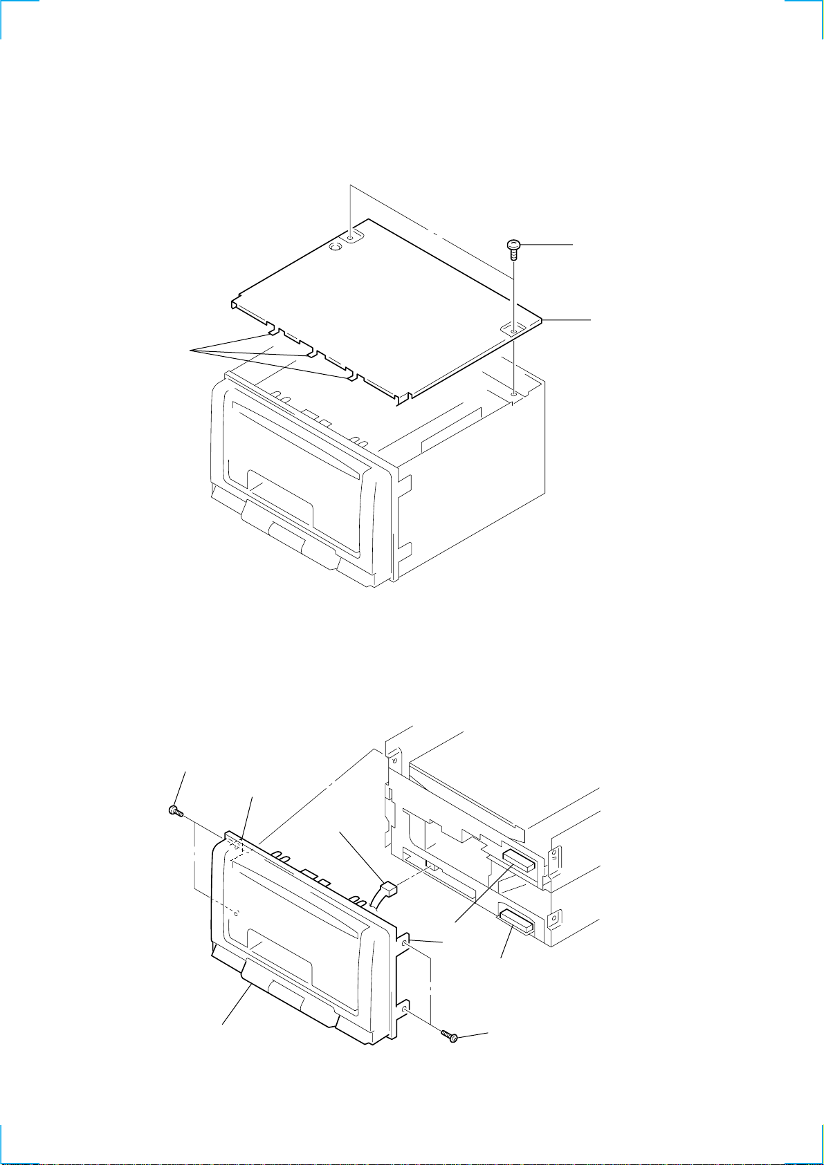
2-1. COVER
2 claws
1 PTT 2.6x5
3 cover
2-2. FRONT PANEL ASSY
1 PTT 2.6x5
3 claw
8 front panel assy
7 CN501
5 CN801
4 claw
6 CN500
2 PTT 2.6x5
10
Page 11
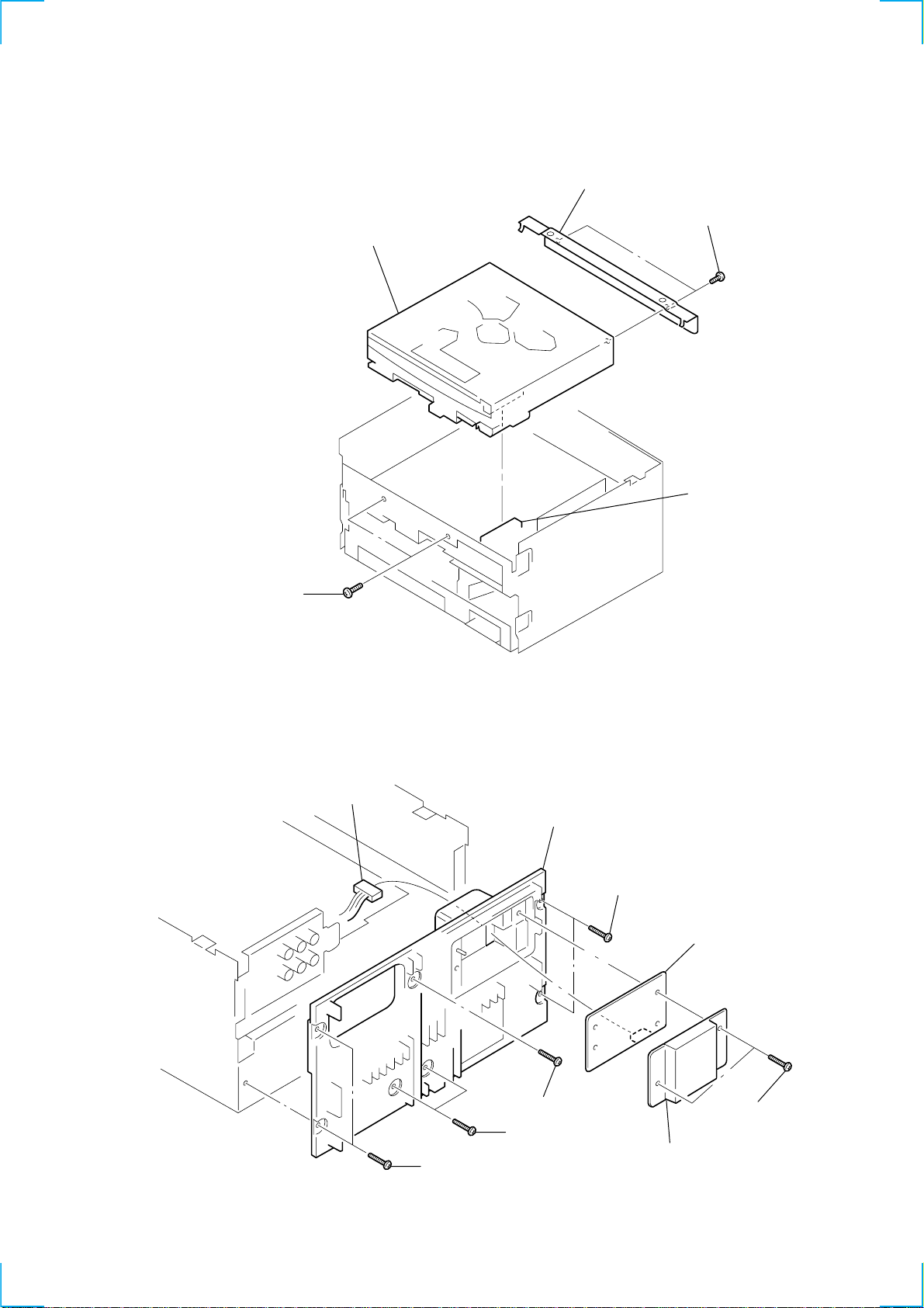
2-3. CD MECHANISM BLOCK
5 bracket (CD)
4 PTT 2.6x5
3 CD mechanism block
2 CN802
1 PTT 2.6x5
2-4. TR BOARD, HEAT SINK
4 CN901
9 heat sink
8 PTT 2.6x12
3 TR board
5 PTT 2.6x12
7 PTT 2.6x12
6 PTT 2.6x12
1 PTT 2.6x10
2 cover (D/D converter)
11
Page 12
2-5. CD BOARD
ground point screw
4
(PTT2.6x6)
3 ground point screw
(PTT2.6x6)
1 CN803
2 CN402
5 CD board
6 insulating sheet (U)
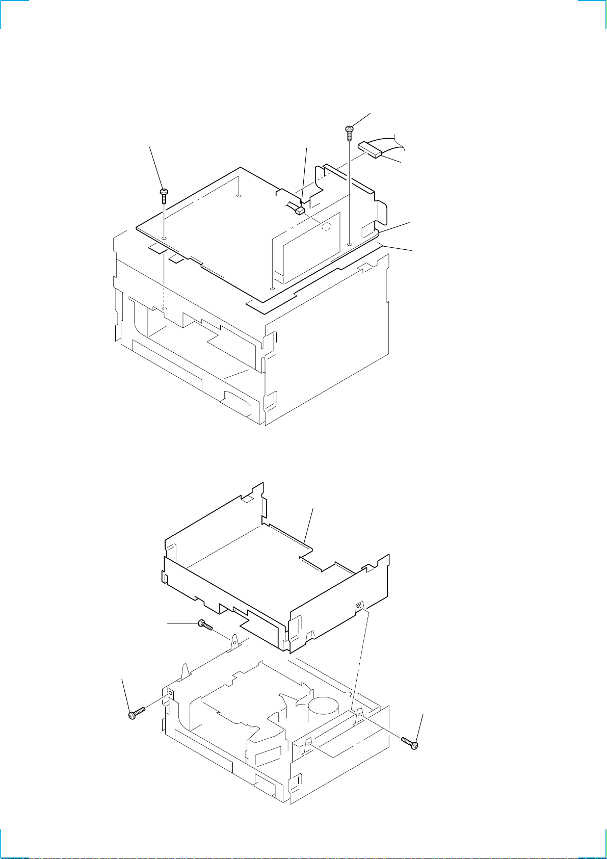
2-6. CHASSIS (U)
4 chassis (U)
2 PTT 2.6x5
1 PTT 2.6x5
3 PTT 2.6x5
12
Page 13
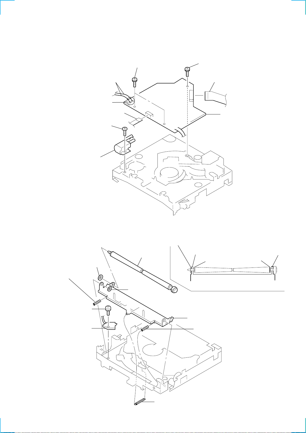
2-7. TAPE MECHANISM BLOCK
5 tape mechanism block
3 CN600
2 PTT 2.6x5
4 CN300
1 PTT 2.6x5
2-8. MAIN BOARD
ground point screw
1
(PTT2.6x6)
ground point screw
2
(PTT2.6x6)
3 MAIN board
4 insulating sheet (L)
13
Page 14
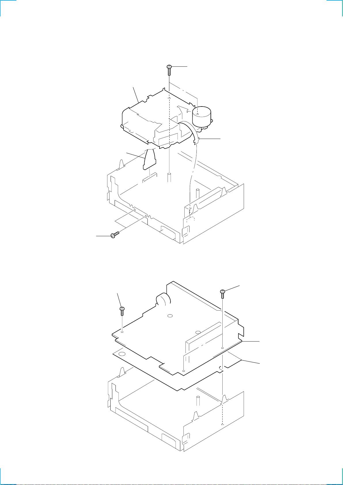
2-9. CHASSIS (TM) ASSY
1 P 2x3
6 chassis (TM) assy
2 P 2x3
3 P 2x3
4 claw
5 CN4
2-10. SENSOR BOARD
1 claw
3 guide (DISC M)
2 claw
4 PS 2x3
5 SENSOR board
14
Page 15
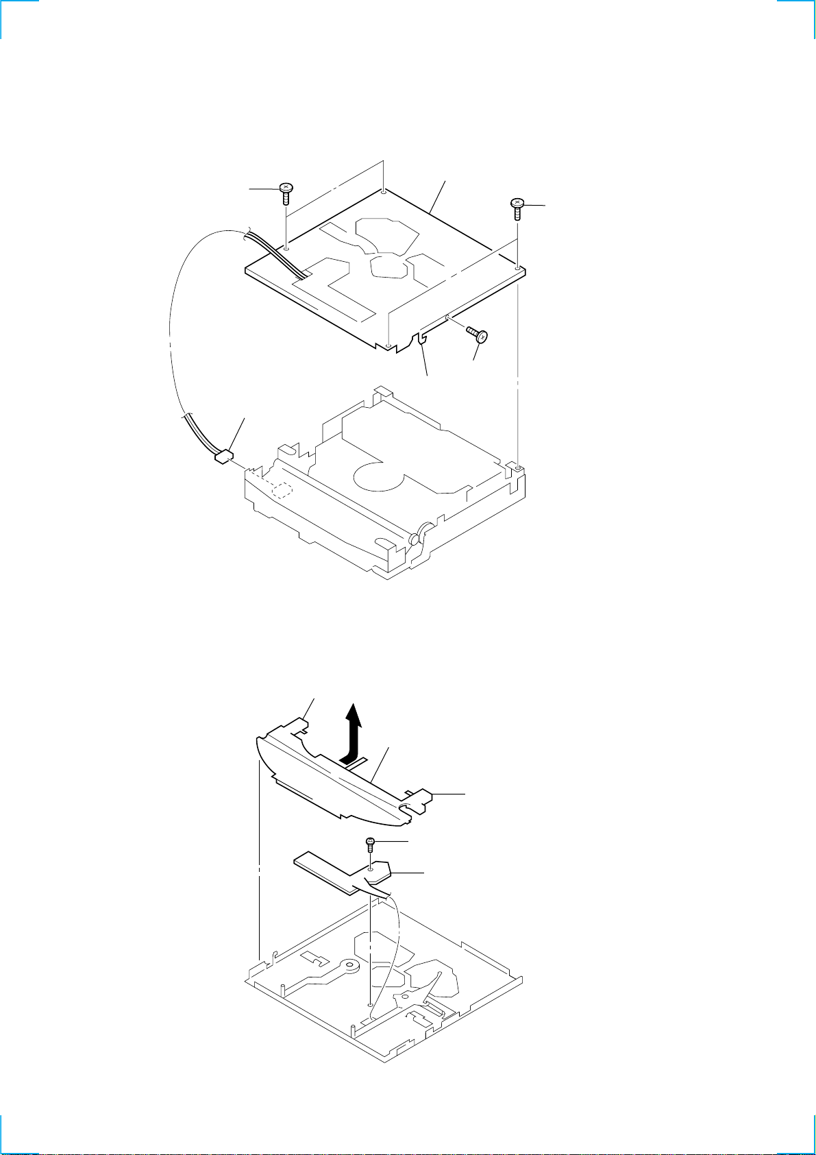
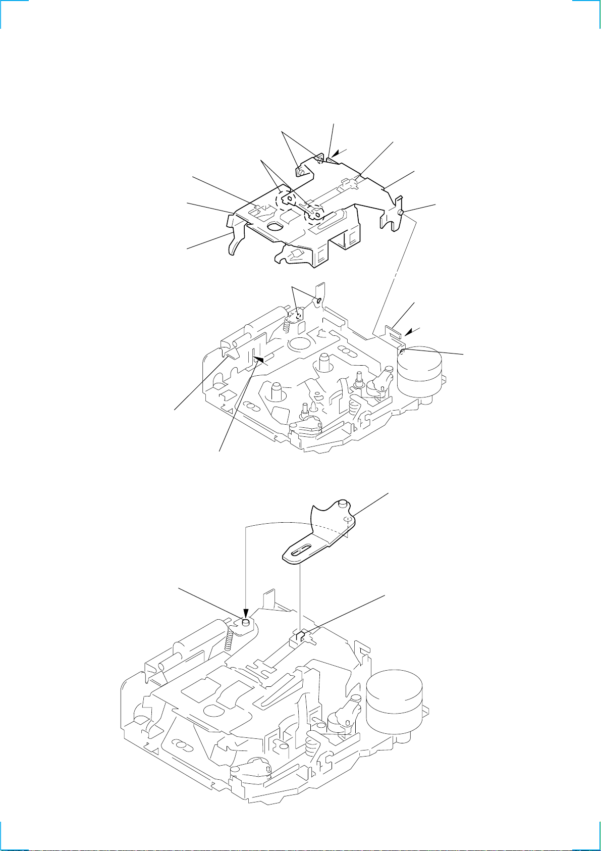
2-11. SERVO BOARD
6
loading motor assy
3
Removal the
two solders.
5
P 2x3
1
4
wires
CN3
7
PS 2x5
8
PS 2x5
2
CN2
9
SERVO board
2-12. ROLLER ASSY
• When installing, take note of the positions
arm (roller) and washers. (Fig. 1)
6 retaining ring (roller)
3 compression spring (RA-L)
8 PS 2x3
9 LOAD board
7 roller assy
4 washer
retaining ring (roller)
arm (roller)
5 arm (roller)
2 compression spring (RA-R)
arm (roller)
washer washer
Fig. 1
1 tension spring (RA-E)
15
Page 16
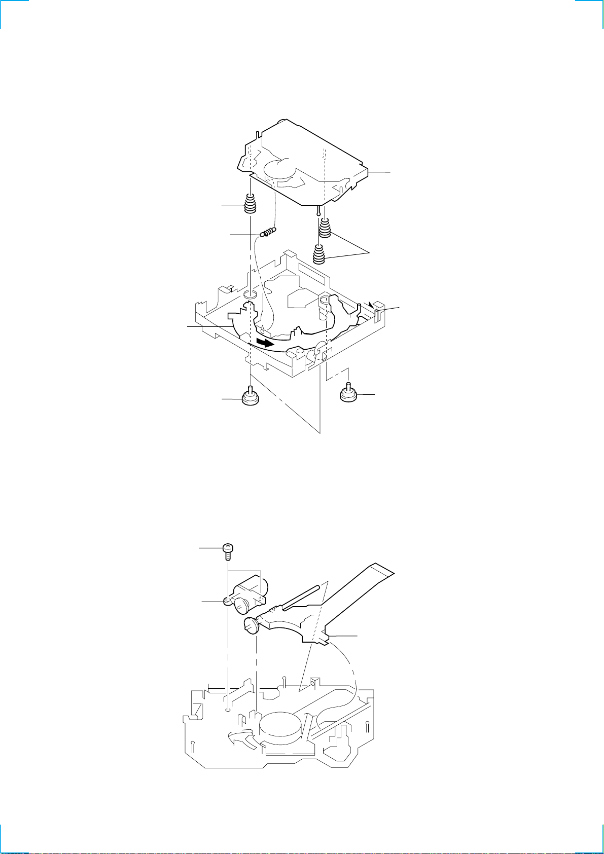
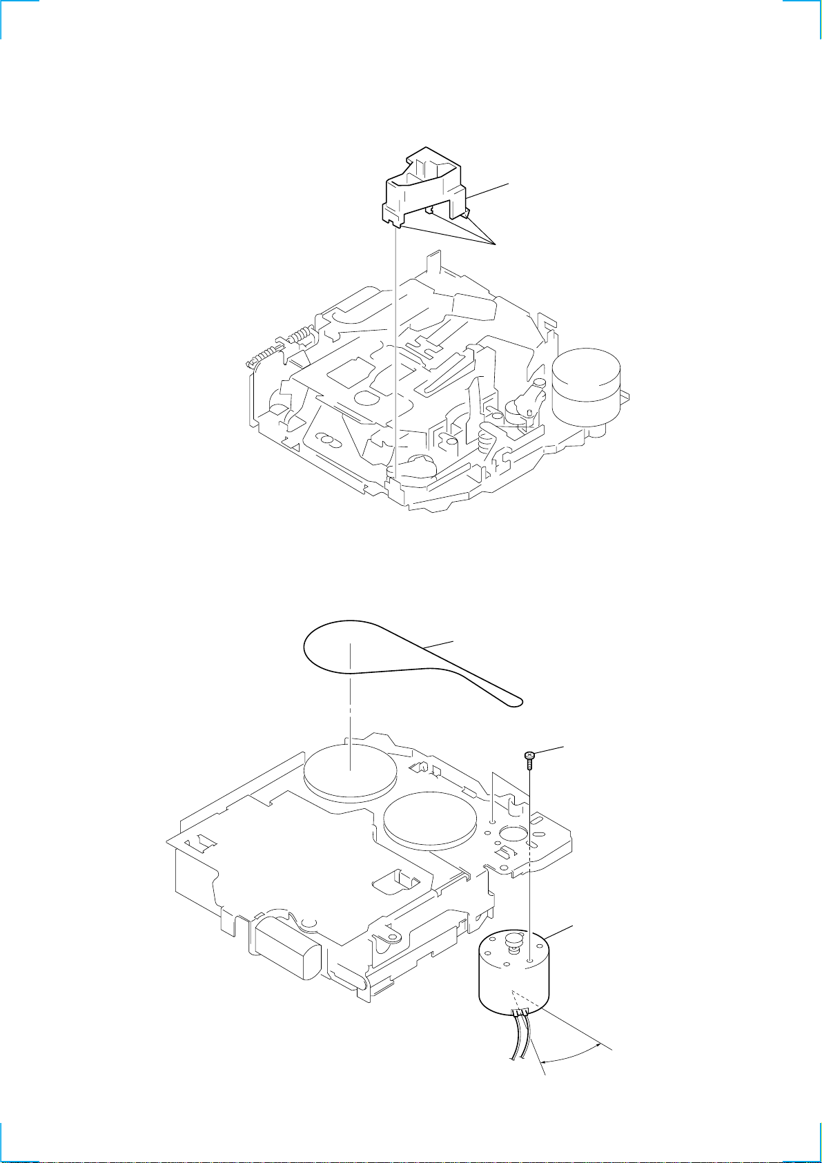
2-13. CHASSIS (OP) (O/S) ASSY
8 compression spring (FL)
1 tension spring (KF8)
5 Turn loading ring in the
direction of the arrow.
6 chassis (OP) (O/S) assy
7 compression spring (FL)
4 Fit lever (D) in the
direction of the arrow.
2 damper (T)
2-14. OPTICAL PICK-UP BLOCK
1 P 2x3
2 sled motor assy
3 damper (T)
3 optical pick-up block
16
Page 17
SECTION 3
ASSEMBLY OF MECHANISM DECK
Note : Follow the assembly procedure in the numerical order given.
3-1. HOUSING
4 Fit claw on B part.
3 Put the housing
under A part.
housing
5 Fit projection on C part.
2 Install the hanger onto
two claws of the housing.
7 Holder the hanger by bending the claw.
1 Install the catcher to the hanger.
hanger
6 Fit projection on D part.
C part
8 Hold the hanger by
bending the claw.
D part
3-2. ARM (SUCTION)
projection
A part
B part
2 Move the arm (suction) in the arrow
Direction and fit on projection.
1 Fit the arm (suction) on the shaft.
17
Page 18
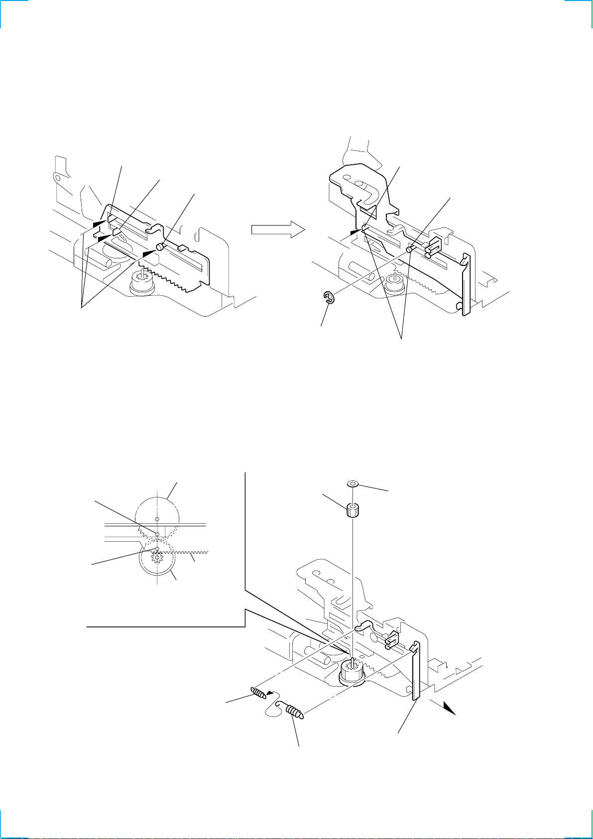
3-3. LEVER (LDG-A) / (LDG-B)
shaft A
1 Fit the lever (LDG-A) on
shafts A to C and install it.
3-4. GEAR (LOADING FT)
shaft B
shaft C
shaft A
shaft B
3 type-E stop ring 2.0
2 Fit the lever (LDG-B) on
shafts A and B and install it.
hole
hole
4 Align hole in the gear (LDG-D)
with hole the lever (LDG-A).
2 tension spring (LD-2)
gear (LDG-D)
lever (LDG-A)
gear (LDG-FB)
5 gear (loading FT)
1
2 tension spring (LD-1)
6 polyethylene washer
3 Move the lever (LDG-B)
in the arrow direction.
18
Page 19
3-5. GUIDE (C)
2 guide (C)
1 claws
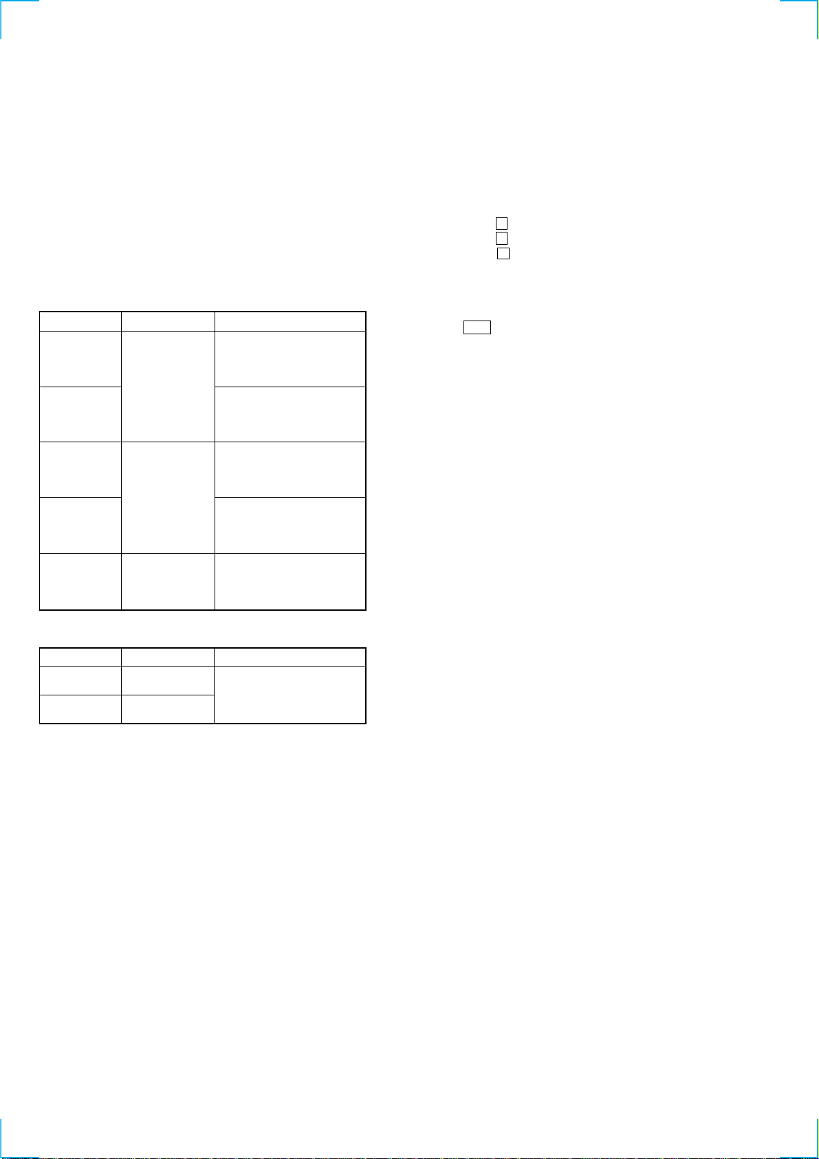
3-6. CAPSTAN / REEL MOTOR (M904)
3 belt (25)
2 precision screws P 2x3
1 main motor assy
(CAPSTAN/REEL) (M904)
30°
19
Page 20
SECTION 4
MECHANICAL ADJUSTMENTS
SECTION 5
ELECTRICAL ADJUSTMENTS
PRECAUTION
1. Wipe the following components with an absorbent cotton cloth
moistened with alcohol before adjustment :
PB head Pinch roller
Idler Rubber belt
Capstan
2. Demagnetize the PB head using a head demagnetizer.
3. Be careful not to use a magnetized screwdriver.
4. After the adjustment is completed, lock the adjustment parts
using screws.
5. Unless otherwise specified, make adjustments at the specified
voltage (14.4 V).
Torque Measurement
Mode Torque Meter Meter Reading
2.95 – 6.37 mN • m
FWD (30 – 65 g • cm)
CQ-102C
FWD
Back T ension
REV (30 – 65 g • cm)
CQ-102RC
REV
Back T ension
FF, REW CQ-201B (60 – 200 g • cm)
(0.42 – 0.90 oz • inch)
0.05 – 0.44 mN • m
(0.5 – 4.5 g • cm)
(0.01 – 0.06 oz • inch)
2.95 – 6.37 mN • m
(0.42 – 0.90 oz • inch)
0.05 – 0.44 mN • m
(0.5 – 4.5 g • cm)
(0.01 – 0.06 oz • inch)
5.89 – 19.61 mN • m
(0.83 – 2.78 oz • inch)
TEST MODE
This set have the test mode function. In the test mode, FM Auto
Scan/Stop Level and AM Auto Scan/Stop Le vel adjustments can be
performed easier than it in ordinary procedure.
<Set the Test Mode>
1. Turn ON the regulated power supply to ACC and BATT
terminals is “OFF” position (display 1:00).
2. Push the preset 4 button.
3. Push the preset 5 button.
4. Press the preset 1 button for more than two seconds.
5. Then the display and LED on the front panel indicates all lights,
the test mode is set.
<Release the Test Mode>
1. Push the OFF button.
T ape T ension Measurement
Mode Tension Meter Meter Reading
FWD CQ-403A
REV CQ-403R
882.60 mN
(more than 90 g)
(more than 3.17 oz)
20
Page 21
See the adjustment location from on page 23 for the
adjustment.
TAPE SECTION
0 dB = 0.775 V
Tape Speed Adjustment
Procedure :
1. Put the set into the FWD PB mode.
test tape
WS-48A
(3 kHz, 0 dB)
set
AUDIO OUT REAR
frequency counter
10 kΩ
TUNER SECTION
0 dB = 1 µV
Cautions during repair
When the tuner unit is defective, replace it by a new one because
its internal block is difficult to repair.
Note on Adjustment
The adjustments of tuner section, should be performed according
to the following sequence.
1. FM Auto Scan/Stop Level Adjustment
2. FM Stereo Separation Adjustment
3. AM Auto Scan/Stop Level Adjustment
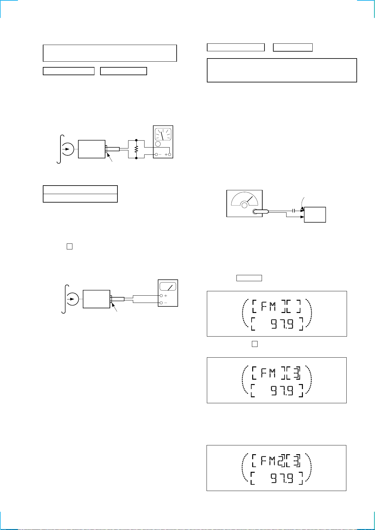
FM Auto Scan/Stop Level Adjustment
Setting :
SOURCE button : FM
FREQUENCY SELECT switch : FM 200k
Specification : Constant speed
Frequency counter
3,010 to 3,030 Hz
Adjustment Location : Capstan motor internal volume
(See page 23)
DOLBY Level Adjustment
Setting :
Preset 3 (SHUF/;) button : Light down mark ;
(DOLBY OFF)
test tape
P-4-D400
(400 Hz, 0 dB)
set
main board
TP-L
TP-R
level meter
Procedure :
1. Put the set into the FWD PB mode.
2. Adjust RV100 (L-CH) and RV200 (R-CH) on main board so
that level meter reading is – 6 ± 0.5 dB (0.37 to 0.41 V).
Adjustment Location : See page 23.
FM RF signal
generator
antenna
0.01 µF
Carrier frequency : 97.9 MHz
Output level : 22 dB (12.6 µV)
Mode : mono
Modulation : 1 kHz, 22.5 kHz deviation (30%)
terminal
Procedure :
1. Set to the test mode.
2. Push the SOURCE button and set to FM.
Display
SHUF1
3. Push the preset 3 button.
Display
PRESET
SHUF1
set
4. Adjust with the volume RV2 on TU1 so that the “FM”
indication turns to “2” indication on the display window.
But, in case of already indicated “2”, turn the RV2 so that put
out light “2” indication and adjustment.
Display
PRESET
SHUF1
Adjustment Location : See page 23.
21
Page 22

FM Stereo Separation Adjustment
Setting :
SOURCE button : FM
FREQUENCY SELECT switch : FM 200k
FM RF signal
generator
0.01 µF
Carrier frequency : 97.9 MHz
Output level : 70 dB (3.2 mV)
Mode : stereo
Modulation : main :1 kHz, 33.75 kHz deviation (45%)
sub :1 kHz, 33.75 kHz deviation (45%)
19 kHz pilot : 7.5 kHz deviation (10%)
antenna
terminal
set
AUDIO OUT REAR
level meter
10 kΩ
AM Auto Scan/Stop Level Adjustment
Note : This adjustment should be performed after the FM Auto
Scan / Stop Level Adjustment is done.
Setting :
SOURCE t MODE button : AM
FREQUENCY SELECT switch : AM 10k
15 pF
30 Ω
65 pF
AM RF signal
generator
AM dummy
antenna (50 Ω)
set
set
Procedure :
FM stereo
signal generator
output channel
Level meter Level meter
connection reading (dB)
L-CH L-CH A
R-CH L-CH Adjust RV4 on TU1 for
maximum reading.
R-CH R-CH C
L-CH R-CH Adjust RV4 on TU1 for
maximum reading.
L-CH stereo separation : A – B
R-CH stereo separation : C – D
The separations of both channels should be equal.
Specification : Separation more than 28 dB
Adjustment Location : See page 23.
B
D
Carrier frequency : 1000 kHz
Output level : 30 dB (44.7 µV)
Mode : mono
Modulation : 1 kHz, 22.5 kHz deviation (30%)
Procedure :
1. Set to the test mode. (See page 20.)
2. Push the SOURCE button.
3. Push the MODE button and set to AM.
Display
SHUF1
4. Push the preset 3 button.
Display
PRESET
SHUF1
antenna
terminal
22
5. Adjust with the volume RV1 on TU1 so that the “AM”
indication turns to “2” indication on the display window. But,
in case of already indicated “2”, turn the RV1 so that put out
light “2” indication and adjustment.
Display
PRESET
SHUF1
Adjustment Location : See page 23.
Page 23

J
Adjustment Location :
– set lower view –
DOLBY
LEVEL
ADJ
RV200
(R-CH)
RV100
(L-CH)
– set upper view –
TP-R
DOLBY LEVEL
TP-L
TAPE SPEED ADJ
TU1
ADJ
RV1 AM AUTO SCAN/STOP LEVEL AD
RV2 FM AUTO SCAN/STOP LEVEL ADJ
RV200 (R-CH) DOLBY LEVEL ADJ
RV4 FM STEREO SEPARATION ADJ
RV100 (L-CH) DOLBY LEVEL ADJ
23
Page 24

CD SECTION
Note :
1. CD Block basically constructed to operate without adjustment.
Therefore, check each item in order given.
2. Use YEDS-18 disc (3-702-101-01) unless otherwise indicated.
3. Use the oscilloscope with more than 10 MΩ impedance.
4. Clean an objective lens by an applicator with neutral detergent
when the signal level is low than specified value with the
following checks.
Focus Bias Adjustment
Setting :This adjustment is performed with the set placed
horizontally.
oscilloscope
(DC range)
servo board
TP (RF)
TP (RF GND)
Procedure :
1. Connect an oscilloscope between TP (RF) and TP (RF GND)
on the servo board.
2. Connect the power supply.
3. Push the RESET button (SW701) on the control board.
4. Insert the disc (YEDS-18) and playback.
5. Adjust RV1 so tha t the oscilloscope waveform is clear and check
RF signal level is correct or not.
Note : Clear RF signal waveform means that the sharp “ ” can be
clearly distinguished at the center of the waveform.
Focus Gain Adjustment (Coarse adjustment)
This adjustment is not required unless the following parts are
replaced:
• Optical pick-up
•RV4
Procedure :
1. Set RV4 to the standard position. (mechanical center)
2. Check whether operation noise (while noise type) caused by
the 2-axis device (lens section of the optical pick-up) is
abnormally loud.
If the operation noise is too loud, turn RV4 slightly counterclockwise.
• If the gain is too low :
Focus does not function and no music is selected.
• If the gain is too high :
Noise caused by scratches and dust is heard and the operation
becomes unstable.
Adjustment Location : servo board (component side)
FOCUS GAIN ADJ
RV4
IC3
CN2
RF signal waveform
VOLT/DIV : 200 mV
TIME/DIV : 500 nS
RF level :
1.0 – 1.5 Vp-p
• When observing the eye pattern, set the oscilloscope to A C range
and raise the vertical sensitivity so that it may be easily seen.
CN1
IC1
TP
(RF GND)
IC2
TP
(RF)
CN3
RV1
FOCUS BIAS ADJ
24
Page 25

SECTION 6
DIAGRAMS
6-1. IC PIN DESCRIPTIONS
• IC500 µPD78058GC-B51-8BT (SYSTEM CONTROL)
Pin No. Pin Name I/O Pin Description
1 VSM I FM, AM common signal meter A/D conversion input
2 NIL I Not used. (Connect to ground in this set.)
3 SD-IN I Station detecter input (“H” : with SD)
4 AVSS — Analog ground
5 FM-ST I FM stereo input pin (“L” : stereo)
6 AM-ST I AM stereo input pin (“L” : stereo)
7 AVREF — Reference power supply for D/A conversion.
8 PLL-SI I PLL serial data input
9 PLL-SO O PLL serial data output
10 PLL-CKO O PLL serial clock output
11 PLL-CE O PLL serial chip enable output
12 AMS I Music with/without detection input at AMS. (“L” : with music, “H” : without music)
13 PLAY/AMS O Tape AMS control output
14 F/R O FWD/REV detection output (“H” : FWD, “L” : REV)
15 MTL O Metal control output (“H” : metal)
16 BUS-SI I Uni-link serial interface data input
17 BUS-SO O Uni-link serial interface data output
18 BUS-CKI I Uni-link serial interface clock input
19 BUS-CKO O Uni-link serial interface clock output
20 TAPE-MUTE O Tape mute control output
21 DOLON I/O Dolby control input/output
22 EQ-CE O Equalizer serial chip enable output (Not used in this set.)
23 EQ-CLK O Equalizer serial clock output (Not used in this set.)
24 DATA O Serial data output
25 VOL-CLK O Electronic volume serial clock output
26 VOL-CE O Electronic volume serial chip enable output
27 MUT O System mute control output
28 AMP-ON O Power amplifier power supply control output
29 AUX-MUT O AUX mute control output
30 C/B I/O Dolby B/C select control output (Not used in this set.)
31 PWR-SEL I Power select initial setting input
32 TEST I Test mode setting input
33 VSS — Ground
34 NIL I Not used. (Connect to ground in this set.)
35 POWER-ON O System power supply control output
36 TUN-ON O Tuner power supply control output
37 FM-ON O FM power supply control output
38 AM-ON O AM power supply control output (Not used in this set.)
39 NIL I Not used. (Connect to ground in this set.)
40 CM-ON O Capstan motor control output
41 TP-ON O Tape power supply control output
42 LM-EJ O Loading motor control output (Eject direction)
43 LM-LOD O Loading motor control output (Loading direction)
44, 45 POS1, 0 I Position signal detection input 1, 0
46 BEEP O Buzzer control output
47, 48 POS2, 3 I Position signal detection input 2, 3
49 REL I Reel stand rotation detection input
50 RC-IN1 I Rotary commander A/D conversion input 1
51 SUB-CE O Sub serial chip enable output (Not used in this set.)
52 SUB-DATA O Sub serial data output (Not used in this set.)
53 SUB-CLK O Sub serial clock output (Not used in this set.)
25
Page 26

Pin No. Pin Name I/O Pin Description
54 SYS-RST O System reset signal output
55 BUS-ON O Bus ON control output
56, 57 RE1, 0 I Rotary encoder input 1, 0
58 AD-ON O Power supply output for A/D conversion.
59 RAMBU I RAM reset detection input
60 RESET — Reset input
61 SIRCS I Remote control input (Not used in this set.)
62 BU-IN I Backup power detection input
63 NIL — Not used (Connect to ground in this set.)
64 ACC-IN I Accessory power supply detection input
65 DIMMER I Dimmer control input
66 TEL-MUTE I Telephone mute control input
67 KEY-ACK I Key input acknowledge
68 VDD — µ-con power supply
69 X2 O Main ceramic oscillator output (5 MHz)
70 X1 I Main ceramic oscillator input (5 MHz)
71 IC — Connect to ground in this set.
72 XT2 O Sub crystal oscillator output (32.768 kHz)
73 XT1 I Sub crystal oscillator input (32.768 kHz)
74 AVDD — Power supply for A/D conversion.
75 AVREF — Reference power supply for A/D conversion.
76, 77 KEY-IN0, 1 I Key input 0, 1
78 KEY-IN2 I Key input 2 (Not used in this set.)
79 RC-IN0 I Rotary commander A/D conversion input 0
80 DSTSEL I Initial setting input of destination.
26
Page 27

• IC801 µPD78054GC-A32-8BT (CD SYSTEM CONTROL)
Pin No. Pin Name I/O Pin Description
1 LEDCLK — Not used in this set.
2 LEDCKO — Not used in this set.
3 LEDSO — Not used in this set.
4 AVSS — Analog ground
5 FL-CE0 O Display driver chip select output 0
6 FL-CE1 O Display driver chip select output 1 (Not used in this set.)
7 AVREF1 — Reference power supply for D/A conversion.
8 FL-RST O Display driver reset output (Not used in this set.)
9 FL-SO O Display driver data output
10 FL-CKO O Display driver clock output
11 SRDT — Not used in this set.
12 NCO — Not used.
13 SCLK — Not used in this set.
14 FL-BLK O Display driver blank control output
15 NIL — Not used. (Connect to ground in this set.)
16 UNISI I Uni-link serial interface data input
17 UNISO O Uni-link serial interface data output
18 UNICKI I Uni-link serial interface clock input
19 LINKOFF O Link off output
20 ILLON O Illumination power supply control output
21 CMDON O CD mechanism power supply control output
22 CD-ON O CD power supply control output
23 SP-SEL O Signal (L/R channel) select control signal output to spectrum analyzer control IC.
24 SP-C O Frequency select control signal output to spectrum analyzer control IC.
25 SP-B O Frequency select control signal output to spectrum analyzer control IC.
26 SP-A O Frequency select control signal output to spectrum analyzer control IC.
27 CDMUT O CD mute control output
28 EMPH-O O Emphasis control output
29 CD-RST O CD signal process IC reset output
30 XMODE — Not used in this set.
31, 32 NIL — Not used. (Connect to ground in this set.)
33 VSS — Ground
34 TBTGSEL I CD tracking balance, tracking gain auto adjustment select input.
35 – 39 NIL — Not used. (Connect to ground in this set.)
40 GFS I GFS signal detection input
41 SQ-SI I SUB Q data input
42 SQ-CKO O SUB Q clock output
43 NIL — Not used. (Connect to ground in this set.)
44 CD-SO O CD signal process serial data output
45 CD-LAT O CD signal process latch output
46 CD-CKO O CD signal process serial clock output
47 PH2 I 8/12 cm disc detection input
48 F-OK I Focus signal detection input
49 LD-ON O Laser on/off select control output
50 D-SW I Down switch detection input
51 PH1 I Disc insert detection input
52 L-SW I Sled limit switch input
53 LM-LOD O Loading motor control output (Loading direction)
54 LM-EJ O Loading motor control output (Eject direction)
55 PH3 I Disc detect sensor input
56 CTL1 O Driver IC control output
57 NCO — Not used.
27
Page 28

Pin No. Pin Name I/O Pin Description
58 EESIO O Not used in this set.
59 EECKO O Not used in this set.
60 RESET — Reset input
61 SCOR I SCOR signal detection input
62 CNIN I Track jump count input
63 SELF-SW I Disc self store detection input
64 SENS I SENS signal detection input
65 DQSY — Not used in this set.
66 BUIN I Backup power supply detection input
67 BUSON I Bus on control input
68 VDD — µ-con power supply
69 X2 O Main ceramic oscillator output (5 MHz)
70 X1 I Main ceramic oscillator input (5 MHz)
71 IC — Not used. (Not used in this set.)
72 XT2 O Sub crystal oscillator output (Not used in this set.)
73 XT1 I Sub crystal oscillator input (Connect to ground in this set.)
74 AVDD — Power supply for A/D conversion.
75 AVREF — Reference power supply for A/D conversion.
76 NIL — Not used. (Connect to ground in this set.)
77 SP-IN I Spectrum analyzer control signal input from spectrum analyzer control IC.
78 TSTIN0 I LOAD/EJECT prohibition setting input
79 NCO — Not used.
80 LEDOE — Not used in this set.
28
Page 29

WX-C5000
MAIN
1
SECTION
(Page 31)
: CD
Signal path
IC801(1/2)
CD SYSTEM CONTROL
28 EMPHOD
27 CDMUT
DET
DISC IN
51
PH1
Q11,D12
DET
Q12,D11
DISC SIZE
47
PH255PH3
LOADING
COMPLETION
SCOR
GFS
40
61
Q13,D10
BATT
8V REG
Q851,852
MD8V
5V REG
Q853,854
SERVO 5V
Q807
22
CD ON
SQ SI42SQ CKO64SENS44SO
41
21
CMDON
Q803
CD
LAT46CKO
45
SW1
63
SELFSW
CDRST
29
(SELF)
F OK
48
CNIN
62
SW4
50
DSW
LDON
49
(DOWN)
LMLOD
53
LMEJ
54
52
LSW
SW3
(LIMIT)
CTL1
56
Q806
R-CH
9ROUT
12LOUT
IC401
D/A CONVERTER
DATA
CLKO
XTI
1
4 LRCK
5
6 BCK
19
21PCMD
20LRCK
22BCK
34XTAI
IC1
57 XLTO
14 RF
59 CLKO
56 DATO
DIGITAL SIGNAL PROCESSOR
IC2
RF AMP, SERVO CONTROL
50 XRST
31RFO
19CLK
20XLT
21DATA
22XRST
E
PD2
F
39
35 PD1
36
38
SERVO 5V
X401
17
EMPH
16.9MHz
55 CNIN
23
C. OUT
FE BIAS
37
RV1
Q804
18
MUTE
XTO
20
1FOK
3 MDP
54 SEIN
24SENS
25FOK
FEO
1
RV4
FOCUS BIAS
FEI
2
34 PD
FOCUS GAIN
29 29
43
27
GFS
SCOR
6FEO
16SLO
13TAO
LD DRIVE
33 LD
Q1,2
19CH1 IN
22CH2 IN
IC3
DRIVE, MOTOR DRIVE
FOCUS/TRACKING COIL
16 CH2+
15 CH2–
24CH3 IN
18 CH1+
3CH4 IN
17 CH1–
13 CH3+
M902
M
46
SQSO
14 CH3–
(SLED)
47
SQCK
49
51
SENS52DATA
12 CH4+
M
M901
XLAT
11 COM
(SPINDLE)
53
CLOK
M
M903
10 CH5+
(LOADING)
6FWD
4CTL1
7REV
5CTL2
04
I - V
AMP
KSS-521A
OPTICAL PICK-UP
6-2. BLOCK DIAGRAM — CD SECTION —
PD
LD
TRACKING
FOCUS
Page 30

MAIN
SECTION
(Page 31)
IC701
FL DRIVER
CE
98
5
CEO
)
2/2
(
IC801
CD SYSTEM CONTROL
IC802
SA CONTROL
3
SA
)
2/2
(
IC500
SYSTEM CONTROL
F/R
MTL
14
18
19
FWD/REV
MTL/NORMAL
IC300
TAPE EQ/DOLBY NR
32
FL701
FL
DRIVER
Q702-704
2
3
2GB
3GB
CL 1GB
BLK
DATA
99 1
97
100
9
14
SO
BLK
FL FL
SP IN CKO
17 77 10
AIN AOUT
8
DOL ON
211315
MAIN SECTION
TAPE L-CH
24
16
L OUT
NR ON
DOLBY
EQ
R-CH
ABCSEL
2
NR
FL+
11 12 1410
TAPE MUTE
20
(Page 31)
17
MUTE/TAPE
AMS OUT
AUTO
34
23
AMS
12
14
MUSIC
+3V REG
POWER
SP
SENSOR
Q901
Q856
CONTROL
BU5V
A26B25C24SEL
PLAY/AMS
20
AMS/PLAY
R-CH
R-CH
DRIVER +5V
Q701
+5V REG
KEY
76
IN0
27 29
MATRIX
77
IN1
KEY
+10V REG
Q857, 858
BATT
KEY
ACTIVE
58
AD ON
POS0
POS1
45
44
RV100
DOLBY LEVEL
CONTROL
Q859, 860
ILL POWER
Q504, 505
67
KEY ACK
POS2
POS3
47
48
TAPE
MECHANISM
(L-CH)
REF VOLTAGE
REL
49
BLOCK
AVREF
Q805
CONTROL
BU5V
J500
(REMOTE IN)
50
IN179IN0
RC
LM EJ
LM LOD
424340
4
2
DRIVE
MOTOR
LOADING
7
9
BATT
MOTOR DRIVE
CAPSTAN/REEL
M
M904
(CAPSTAN/REEL)
Q802
IC600
Q603, 604
20
ILL ON
UNISI
BUS ON
16
67
55ON16SI17SO18
BUS
CM ON
VR771
TAPE POWER
UNICKI
66
18
19
62
CKI
CKO
BU IN
RE1
RE0
565741
JOG
ENCODER
BATT
CONTROL
Q601, 602
Q600
+8.5V REG
+8.5V
X801
RESET X2X1BU IN
60 69
54
60
RESET
SYS RST
TP ON
5MHz
70
35
POWER ON
RST
IC620
BUS INTERFACE
RST
BATT
Q620
DET
Q620
BATT
IC501
RESET
1
RESET
UNISO
17
LINK OFF
19
SW701
3030
Q801
9
8
11
IN
IN
564
231
OUT
BUS
DATA
6
CN620
(BUS CONTROL IN)
ON
BUS
ON
1 12
Q621
8
CLK
BATT
CHECK
CLK
2 13
3 10
4
D622
7
BATT
6-3. BLOCK DIAGRAM — TAPE SECTION —
WX-C5000
HP901
L
PLAYBACK HEAD
FWD
L
R
R
Signal path
REV
: TAPE (PB)
04
Page 31

WX-C5000
FL+
FL–
RL+
IC331
31
TONE
383635
18
ANT AM L-CH OUT
1
RL–4FR+12FR–3RR+11RR–
2
10
9
7
RL+
RL–
RL IN
11
Q190
(Page 30)
20
RL
OUT
SEL OUT
L
R
SEL OUT
CE
CL
DI
37
TAPE L-CH
2
CD
TAPE
SECTION
(Page 30)
R-CH
16
12
AM DET
R-CH OUT
ANT FM R-CH
2
4 22
STNBY MUTE
TAPE
VC BUFFER
17 16 18 44 34
CD L-CH
1
SECTION
R-CH
3
SECTION
SA
1
IC341
2
3
(Page 29)
FM8V
D1
8
9
+8V TU
+8V FM
D657
Q340
SA MUTE
IC500 (1/2)
SYSTEM CONTROL
VSM DATA
1 24
Q3
S-METER
AM8V
10
19
+8V AM
S-METER
BATT
DET
MUTE
Q651,652
25
26
VOL CE
VOL CLK
FM ST5SD IN
3
20SD22ST13
R654
Q655
MUTE
DRIVE
Q500
MUTE
SWITCH
46
27
MUT
BEEP
X1
1
XI
IC1
PLL
SEEK
7
SEEK
1
9
CN651
AUDIO OUT
REAR
FRONT
L
R CN401(2/2)
L
-3
-6
-5
R-CH
-4
R
POWER AMP
R-CH
5
3
FL+
FL–
IC751
FL IN
12
Q180
21
FL
OUT
IC350
ELECTRONIC VOLUME
R-CH
–2
–1
CN401(1/2)
BUS AUDIO IN
L
R
LPF
TU1
TUNER INIT
D659
BATT
7.2MHz
20
XO
AM IF
13
11
IFC AM
BATT
DET
Q653
28
29
AMP ON
AUX MUT
21
IFC FM
15
TEST
32
TEST
AM OSC15FM OSC SI
6
VCO
D663
8
6
DATA OUT
16
ACC14ILL13ATT16BATT
7
F901
Q654
Q501
ACC DET
Q503
SWITCH
DIMMER
64
65
66
ACC IN
DIMMER
TEL MUTE
PLL
SD
CKO
CE
9
10
11
5
4
2
CE
CLK
DATA IN
LO/DX
PD
9
18
LPF
Q1, 2
4
5
VT
LO/DX
BATT
BATT
IC680
POWER SUPPLY
MODE2 VCC
2 7
36
TUN ON
X269X1
70
X500
5MHz
ANT REM5AMP REM
6
8
ANT+B
AMP+B
BU+B9COM8V
MODE1
3
5
BU5V
PULL-UP+5V
RAM
RESET
1
37
59
FM ON
RAMBU
XT2
XT173PWR SEL
72
X501
32.768KHz
Signal path
: FM
: AM
6
AM8V11FM8V
10
FM8V
AM8V
COM8V
FM200K
IC502
BU.5V
31
B
A
S501
(POWER SELECT)
: TAPE (PB)
: CD
S502
FREQUENCY
( )
AM10K
80
DSTSEL
SELECT
FM50K
AM9K
31 31
J1
6-4. BLOCK DIAGRAM — MAIN SECTION —
(ANTENNA)
04
Page 32

Ref. No. Location
IC1 D-2
Location
(SERVO Board)
• Semiconductor
IC2 D-5
IC3 B-2
Q1 F-4
Q2 F-5
Q11 E-4
Q12 F-3
Q13 F-1
W or less unless otherwise
4
/
1
: Through hole.
: internal component.
f
a
(The other layer’s patterns are not indicated.)
Caution:
Pattern face side: Parts on the pattern face side seen from the
(Side B) pattern face are indicated.
Parts face side: Parts on the parts face side seen from the
•
THIS NOTE IS COMMON FOR PRINTED WIRING BOARDS
AND SCHEMATIC DIAGRAMS.
(In addition to this, the necessary note is
printed in each block.)
Note on Printed Wiring Boards:
• b : Pattern from the side which enables seeing.
• X : parts extracted from the component side.
• Y : parts extracted from the conductor side.
•
(Side A) parts face are indicated.
Note on Schematic Diagram:
• All capacitors are in µF unless otherwise noted. pF: µµF
CD board
LIMIT board
TR board
SUB board
: internal component.
f
specified.
50 WV or less are not indicated except for electrolytics
and tantalums.
• % : indicates tolerance.
•
• All resistors are in Ω and
Replace only with part number specified.
with mark 0 are critical for safety.
Note: The components identified by mark 0 or dotted line
• C : panel designation.
supply from ACC and BATT cords.
• U : B+ Line.
• H : adjustment for repair.
• Power voltage is dc 14.4V and fed with regulated dc power
• Voltage and waveforms are dc with respect to ground
under no-signal conditions.
Voltage variations may be noted due to normal produc-
tion tolerances.
• Voltages are taken with a VOM (Input impedance 10 MΩ).
SERVO board
MAIN board
CONTROL board
Voltage variations may be noted due to normal produc-
tion tolerances.
F : FM
f : AM
E : TAPE (PB)
• Signal path.
J : CD
• Waveforms are taken with a oscilloscope.
• Circled numbers refer to waveforms.
3232
6-5. CIRCUIT BOARDS LOCATION
SENSOR board
LOAD board
JOG board
Page 33

WX-C5000
6-6. PRINTED WIRING BOARDS — CD MECHANISM SECTION —
SW1
PICK-UP
OPTICAL
11
1-659-881-
PICK-UP FLEXIBLE BOARD
JR05
(CHASSIS)
C40
SERVO BOARD
A
D12
SW1
(SELF)
ON:WHEN THE DISC IS
IN/OUT OPERATION
KSS-521A
1
5
1
7
C39
IC3
28 22 2125 15
DISC IN
DETECT
D12
CN2
JR07
CN1
6
BLU
BLU
SW4
(DOWN)
ON:WHEN COMPLETION
SW4
JR58
B C E
Q2
R16
R17
R19
JR53
JR52
L2
TP(RF)
JR30
JR28
JR29
RED
12
(31)
1
1-659-834-
OF THE DISC
CHUKING OPERATION.
7
WHT
WHT
JR59
JR57
JR56
JR55
R7
B C E
Q1
C9
16
JR54
F
M
3
8
JR02JR31
WHT
-
Q12
Q13
9
5
WHT
WHT
CN3
BLK
RED
YEL
M M
WHT
11
6
1
M903
(LOADING)
M901
M902
(31)
11
(11)
1-660-796-
(CHASSIS)
(CHASSIS)
(SPINDLE)
(SLED)
33 33
234 5 6
1
04
11
1-659-880-
BOARD
(31)
C18
353025
Q11
R47
C36
JR39
L1
521
C17
R20
C16
C23
JR40
JR42 JR43
C7
C1
MOTOR FLEXIBLE
SUB BOARD
LOAD BOARD
BLU
BLK
RED
CN4
13
R9 R8
RV1
JR60
R5
JR41
JR25
R21 R10
R11
R14
R15
C10
C13
C15
C14
C12
JR50
JR47
JR49JR48
JR51
JR45 JR46
JR44
JR37
JR36JR34
JR35
JR22
JR15
JR24
JR27
JR26
E
21
(31)
R12
3
1
2
BLU
BLK
RED
1-660-797-
SW3
(LIMIT)
ON:WHEN THE OPTICAL PICK-UP
IS INNER POSITION.
SW3
1-659-835-
12
LIMIT BOARD
R10
D11
D11
DETECT
DISC SIZE
(8CM/12CM)
R11
D10
DETECT
D10
LOADING COMPLETION
SENSOR BOARD
TP
(RF GND)
R30
R31
C20
C22
R34
C24
R36
C26C27
C30
L3
JR16
51
1
0
1 5 7 8 10 14
JR06
JR08
R23
R24
R22
R51
JR09
JR10
B
C11
JR18
JR17
R40
C38
JR11
C31
JR12
C2
R1 R2
R49 R48
R50
JR03
JR13
JR14
C
R32
R33
BL2
RV4
C25 R35
R37
R38
R39
C28
C29
C32
R41
R42
JR19
JR20
C3
JR23
R3 C4
15
202530
30
10
IC1
40
35
20
25
JR21
D
BLU
BLU
R27
R29
R28
BL1
C19
C21
45
40
1510
IC2
15
20
C35
R46
C34
R45
R43
C33
R44
C5
R6 C6
R4
JR38
5
1
6055
45
50
10
CN1
15
1
CD
CN802
BOARD
(Page 36)
Page 34

(Page 35)
: Impossible to measure
∗
under no-signal conditions.
no mark : CD PLAY
Note:
• Voltage and waveforms are dc with respect to ground
34 34
6-7. SCHEMATIC DIAGRAM — CD MECHANISM SECTION (1/2) — • Refer to page 35 for Waveforms and page 48 for IC Block Diagrams.
WX-C5000
Page 35

WX-C5000
(MODE : CD PLAY)
• Waveforms
1
0V
Approx. 620mVp-p
(FEO)
1
IC2
2
1.2Vp-p
(RFO)
ea
IC2
3
0V
(TEO)
Approx. 200mVp-p
rs
IC2
4
2.6Vp-p
7.6µsec
(MDP)
3
IC1
5
5.8Vp-p
22.7µsec
(LRCK)
w;
IC1
6
5.7Vp-p
(BCK)
474nsec
ws
IC1
(Page 37)
7
3.2Vp-p
(XTAI)
ef
16.89MHz
IC1
under no-signal conditions.
no mark : CD PLAY
Note:
• Voltage and waveforms are dc with respect to ground
35 35
6-8. SCHEMATIC DIAGRAM — CD MECHANISM SECTION (2/2) — • Refer to page 48 for IC Block Diagrams.
(Page 34)
Page 36

(Page 38)
(Page 33)
(Page 45)
36 36
6-11. PRINTED WIRING BOARD — CD SECTION —
6-9. PRINTED WIRING BOARD — TR SECTION —
WX-C5000
(Page 39)
6-10. SCHEMATIC DIAGRAM — TR SECTION —
Location (CD board)
• Semiconductor
(Page 37)
Ref. No. Location
D401 F-4
D801 G-8
D802 G-10
D851 H-2
(Page 37)
D852 I-2
D853 E-2
D854 E-2
D855 E-2
D856 F-3
D857 F-3
D858 F-2
D859 K-3
D860 I-11
D862 J-11
D865 K-10
IC401 F-5
IC801 I-7
IC802 F-8
Q801 G-8
Q802 G-9
Q803 G-7
Q804 F-8
Q805 I-9
Q806 H-3
Q807 G-7
Q811 F-10
Q812 E-10
Q851 H-1
Q852 G-3
Q853 I-1
Q854 H-3
Q856 D-4
Q857 G-1
Q858 F-2
Q859 J-2
Q860 K-2
no-signal conditions.
no mark : CD PLAY
Note:
• Voltage is dc with respect to ground under
Page 37

WX-C5000
(Page 41)
(Page 35)
condition.
no mark : CD PLAY
Note:
• Voltage is dc with respect to ground under no-signal
37 37
6-12. SCHEMATIC DIAGRAM — CD SECTION — • Refer to page 51 for IC Block Diagrams.
(Page 41)
(Page 36)
(Page 36)
(Page 46)
Page 38

(Page 36)
6-13. PRINTED WIRING BOARD — MAIN SECTION —
38 38
WX-C5000
D756 C-8
D757 B-7
D758 B-7
IC1 E-11
IC300 H-10
Ref. No. Location
(D1) F-11
(D500) I-2
Ref. No. Location
• Semiconductor Location
IC331 J-11
(D501) I-3
(D502) F-5
(D503) F-5
D504 K-6
D505 H-6
IC341 F-10
D506 B-12
IC350 H-8
D507 B-12
IC500 J-4
D508 K-11
(IC501) J-3
D509 K-11
IC502 I-2
D510 K-11
(IC600) F-2
(D511) L-4
IC620 F-3
(D512) L-5
(IC680) D-6
D513 H-5
(IC751) A-9
(D514) I-3
D600 D-2
(Q1) D-11
D601 G-2
(Q2) D-12
D602 F-2
Q3 H-13
(D603) E-2
(Q4) F-6
D620 E-2
(Q5) E-6
(D621) E-3
Q180 E-8
(D622) E-3
Q190 E-8
D623 B-2
Q280 E-9
D624 D-3
Q290 E-9
D625 B-2
Q340 D-9
(D651) C-3
Q500 G-5
D652 B-6
Q501 G-4
D653 A-6
Q503 G-4
D654 B-6
Q504 K-6
D656 D-3
Q505 K-6
D657 D-7
(Q600) G-2
D659 E-7
Q601 G-2
D660 C-6
Q602 G-2
D661 C-6
(Q603) E-3
D662 D-3
(Q604) E-2
D663 D-4
Q620 E-2
D664 F-5
Q621 E-3
D680 E-8
Q651 B-7
(D681) E-9
Q652 B-7
D751 C-9
Q653 E-7
D752 C-9
Q654 E-4
D753 C-9
(Q655) E-8
D754 C-8
D755 B-8
( ) : SIDE B
Page 39

WX-C5000
(Page 36)
(Page 47)
39 39
(Page 45)
Page 40

(Page 41)
condition.
no mark : FM
(): AM
Note:
• Voltage is dc with respect to ground under no-signal
(Page 42)
40 40
6-14. SCHEMATIC DIAGRAM — MAIN SECTION (1/4) — • Refer to page 50 for IC Block Diagrams.
WX-C5000
Page 41

WX-C5000
(Page 37)
(Page 37)
(detuned) condition.
no mark : FM
Note:
• Voltage is dc with respect to ground under no-signal
(Page 43)
(Page 42)
41 41
6-15. SCHEMATIC DIAGRAM — MAIN SECTION (2/4) —
(Page 40)
Page 42

(Page 41)
(Page 43)
condition.
no mark : FM
( ) : TAPE PLAY
Note:
• Voltage is dc with respect to ground under no-signal
(Page 40)
42 42
6-16. SCHEMATIC DIAGRAM — MAIN SECTION (3/4) — • Refer to page 50 for IC Block Diagrams.
WX-C5000
Page 43

WX-C5000
(Page 41)
(Page 47)
(Page 46)
condition.
no mark : FM
(): AM
Note:
• Voltage is dc with respect to ground under no-signal
43 43
6-17. SCHEMATIC DIAGRAM — MAIN SECTION (4/4) — • Refer to page 50 for IC Block Diagrams.
(Page 42)
Page 44

(IC701) C-7
Ref. No. Location
(Q701) C-9
(Q702) C-10
(Q703) D-10
44 44
(Q704) C-9
6-18. PRINTED WIRING BOARD — CONTROL SECTION —
WX-C5000
(D701) B-8
(D704) C-10
(D705) C-10
(D706) C-9
D730 F-6
D731 A-7
Ref. No. Location
• Semiconductor Location
D732 F-6
D733 B-12
( ) : SIDE B
Page 45

WX-C5000
(Page 36)
45 45
(Page 39)
Page 46

(Page 37)
(Page 43)
(detuned) condition.
no mark : FM
Note:
• Voltage is dc with respect to ground under no-signal
6-19. SCHEMATIC DIAGRAM — CONTROL SECTION —
46 46
WX-C5000
Page 47

6-20. PRINTED WIRING BOARD — JOG SECTION —
WX-C5000
(Page 39)
6-21. SCHEMATIC DIAGRAM — JOG SECTION —
(Page 43)
47
Page 48

• IC Block Diagrams
IC1 CXD2507AQ (SERVO BOARD)
FOK
MON
MDP
MDS
LOCK
TEST
FILO
FILI
PCO
VSS
AVSS
CLTV
AVDD
BIAS
ASYI
ASYO
ASYE
WDCK
XLON
SPOC
SPOD
63
62
64
1
2
3
4
5
6
7
8
9
10
11
12
13
RF
14
15
16
17
18
19
SERVO AUTO
SEQUENCER
CPU
INTERFACE
14
DIGITAL
PLL
ASYMMETRY
CORRECTOR
5
20 21 22 23 24 25 26 27 293031 3228
BCLK
LRCK
PCMD
16K
RAM
GTOP
VDD
CLKO
SPOB
SPOA
58596061
5
SUB CODE
PROCESSOR
EFM
DEMODULATOR
3
ERROR
CORRECTOR
K
S
D
F
C
D
G
P
V
XUGF
X
XLTO
DATO
5657
4
D/A
INTERFACE
3
K
C
F
C2PO
R
CNIN
5455
XROF
SEIN
53
6
MNT3
CLOK
52
MNT1
XLAT
DIGITAL
CLV
DIGITAL
OUT
CLOCK
GENERATOR
51
DATA
50
XRST
49
SENS
48
MUTE
47
SQCK
SQSO
46
45
EXCK
44
SBSO
43
SCOR
42
VSS
41
WFCK
40
EMPH
39
DOUT
C4M
38
37
FSTT
36
XTSL
35
XTAO
34
XTAI
MNTO
33
IC3 BA6796FP-T1
OP IN –
OP IN +
VREF
CH3
28
1
OPOUT
26
27
THERMAL
CTL1 CTL2 FWD REV
23 4
CH4
CH4-IN
CTL1
SHUT
DOWN
CH1
LEVEL
SHIFT
V/I
TRAY
21
VCC
LEVEL
SHIFT
9
VCC
GND
DRIVE
BUFFER
10
CH5 –
CH2
CH3-IN
2425
LEVEL
SHIFT
LOGIC
5
CTL2
23
6
FWD
CH2-IN
22
78
REV
1920
CH1-IN
DRIVE
BUFFER
DRIVE
BUFFER
11
CH1 +
LEVEL
SHIFT
COM
CH1 –
DRIVE
BUFFER
DRIVE
BUFFER
12 13
CH4 +
161718
DRIVE
BUFFER
DRIVE
BUFFER
CH2 +
CH3 +
15
DRIVE
BUFFER
DRIVE
BUFFER
14
CH2 –
CH3 –
48
Page 49

IC2 CXA1782BQ
FE BIAS
PHD 2
36 35 34
37
F
38
E
39
PHD 1
RF IV AMP1
APC
RF IV AMP2
F IV AMP
PHD
33
FE AMP
LD
RF M
32
FOK
RF O
31
LEVEL S
TTL
IIL
FZC COMP
RF I
30 29 28 27 26 25
MIRR
IIL DATA REGISTER
TOG1-3
FS1-4 TG1-2 TM1-7 PS1-4
BAL1-3
CP
DFCT
INPUT SHIFT REGISTER
ADDRESS DECODER
OUTPUT DECODER
CB
CC1
TTL
TTL
FOK
CC2
IIL
IIL
24
SENS
C.OUT
23
XRST
22
21
DATA
20
XLT
19
CLK
VCC
18
VEE
TED
LPFI
TEI
ATSC
TZC
TDFCT
BAL2
TOG1
TOG2
WINDOW COMP
E IV AMP
BAL 3
ATSC
TOG3
TE AMP
TG1
FS1
TRACKING
PHASE
COMPENSATION
987
TGU
SRCH
TG2
TM7
TM6
TM5
TM4
TM3
TA M
ISET
17
SL O
16
SL M
15
SL P
14
13
TA O
ISET
TM2
F SET
11
10
TG2
12
FSET
HPF COMP
TZC COMP
DFCT
TM1
DFCT
FS4
2
1
FEI
FEO
FDFCT
43
FGD
FCS PHASE
COMPENSATION
5
6
FLB
FE O
LPF COMP
FS2
FE M
EI
40
BAL1
41
42
43
44
45
46
47
VC
48
49
Page 50

IC1 BU2624FV-E2 (MAIN BOARD)
XIN
XOUT
20
19
VSS
PHASE
DET
I/O
CTL
REFERENCE
DIVIDER
SHIFT REGISTER LATCH
MAIN
COUNT
PRESCALER
IF COUNT
CTL
20BIT COUNT
1
2
CE
CK
4
DA
5
CD
6
7
P0
9
P1
10
P3
18
PD
17
VDD
FMIN
16
AMIN
15
P2
14
13
IFIN
12
SD
P4
11
IC331, 341 NJM4558M-T1
A OUT
A IN–
A IN+
VEE
1
A
+–
2
3
4
B
+–
8
VCC
7
B OUT
6
B IN–
5
B IN+
IC300 CXA2510AQ-T4
PBEQ1
–
PBFB1
31
32
PBRIN1
PBREF1
PBFIN1
VCT
PBGND
PBFIN2
PBREF2
PBRIN2
PBFB2
33
34
35
36
37
38
39
40
F2
VCT
F1
1
PBEQ2
AUXIN1
TAPEIN1
PBOUT1
GND
282930
27
120µ/
70µ
+
–
+
120µ/
70µ
345 6 7 8 9 10
2
VCC
PBOUT2
X1
+
X1
TAPEIN2
T1
AUXIN2
T2
NR BIAS
TAPE/AUX
TAPE EQ
FWD/RVS
VCC
LPF
+
–
F3
–
+
MSLPF
LINEOUT2
25
DIREF
OFF/B
+
NR
LINEOUT1
24
–
NC
TCH2
NR
OFF/B
PLAY
TCH1
NC
MSSW
21222326
MS
MODE
NR
MODE
DETECT
MS ON/
OFF
20
19
18
17
16
15
14
13
12
11
MSMODE
DRSW
TAPESW
INSW
NRSW
NC
MSOUT
DGND
MSTC
FF
IC620 BA8270F-E2
BUS ON
1
2
RST
BATT
3
4
CLK
5
VREF
6
DATA
GND
7 8
BUS ON
SWITCH
SWITCH
BATTERY
SWITCH
RESET
14
13
12
11
10
9
VCC
RST
BUS ON
CLK IN
BU IN
DATA IN
DATA OUT
50
Page 51

IC350 LC75374E
LVRIN
34
LSELO
35
L4
L3
36
L2
37
L1
38
39
VDD
R1
40
41
R2
R3
42
R4
43
44
RSELO
1
RVRIN
LT3
LT2
+
–
–
+
LT1
–
+
+
–
+
–
DECODER LATCH
+
–
RT1
RT2
RT3
LCOM
+
–
+
–
–
+
–
+
2 345 6 7 8 9
RCOM
LSIN
LTOUT
CONTROL
REGISTER
RSIN
RTOUT
NC
2627282930313233
SHIFT
NC
LSB2
LSB1
NC
2324
25
22
LFIN
+
–
+
+
–
10
11
NC
RSB1
RSB2
–
+
–
–
+
–
+
LFOUT
21
LROUT
20
19
VREF
18
CE
17
DI
16
CL
15
VSS
14
RROUT
RFOUT
13
12
RFIN
IC401 PCM1717E-ST2
1
XTI
2
DGND
3
VDD
4
LRCIN
DIN
BCKIN
ZERO
D/C R
VOUTR
AGND
5
6
7
8
9
10
INTERFACE
5LEVE DAC
LOWPASS FILTER
CMOS
AMP
CONTROL
INPUT
DIGITAL
FILTER
NOISE SHAPER
CLK
5LEVEL DAC
LOWPASS FILTER
CMOS
AMP
MODE
CONT
ROL
20
19
18
17
16
15
14
13
12
11
XTO
CLKO
ML/MUTE
MC/DM1
MD/DM0
RSTB
MODE
D/C L
VOUTL
VCC
IC502 RN5VD23AA-TL
CD
5
RESET
2 3
1
OUT
VDD
IC600 LB1930M-TLM
VCC
1
BUFFER
NC
2
IN1
IN2
S-GND
3
4
BUFFER
5
CONTROL
CIRCUIT
4
NC
GND
MOTOR
DRIVE
CIRCUIT
NC
10
OUT1
9
8
NC
7
OUT2
P-GND
6
51
Page 52

T
IC802 BA3834F
PEAK
HOLD
68Hz
B.P.F.
1
2
BIASC
VREFC
REGISTER
3
4
RREF
REGISTER
PEAK
HOLD
170Hz
B.P.F.
5
NC
IFOUT
IC680 BA3918-V2
18
PEAK
HOLD
420Hz
B.P.F.
DIFFERENTIAL
AMPLIFIER
6
NC
GND
MULTIPLEXER
REGISTER
7
8
CIN
AIN
PEAK
HOLD
1kHz
B.P.F.
AOU
9
VCC
REGISTER
TEST
1617
PEAK
HOLD
2.4kHz
B.P.F.
NC
15
REGISTER
PEAK
HOLD
5.9kHz
B.P.F.
SEL
13
14
DECODER
REGISTER
C
A
B
NC
1011
12
REGISTER
PEAK
HOLD
14.4kHz
B.P.F.
REGULATOR
OVER VOLTAGE
PROTECT
–
+
2 3
4
1
NC
STB
MODE2
MODE1
5 6 7 8 9
ANT
VCC
VDD
AMP
COM
–
+
10
AM
–
+
11
FM
–
+
12
GND
52
Page 53

NOTE:
• The mechanical parts with no reference
number in the exploded views are not supplied.
• Items marked “*” are not stocked since
they are seldom required for routine service.
Some delay should be anticipated
when ordering these items.
7-1. COVER SECTION
SECTION 7
EXPLODED VIEWS
• -XX and -X mean standardized parts, so
they may have some difference from the
original one.
• Color Indication of Appearance Parts
Example :
KNOB, BALANCE (WHITE) ... (RED)
R
Parts Color Cabinet’s Color
#1
• Accessories and packing materials and
hardware (# mark) list are given in
the last of this parts list.
The components identified by
mark 0 or dotted line with mark
R
0 are critical for safety.
Replace only with part number
specified.
#1
2
6
5
4
#2
#11
1
#2
F901
#2
#2
3
#1
Ref. No. Part No. Description Remark
1 1-791-457-11 CORD (WITH CONNECTOR) (POWER)
* 2 3-024-092-21 COVER
* 3 3-024-091-21 HEAT SINK
* 4 1-676-336-11 TR BOARD
Ref. No. Part No. Description Remark
* 5 3-025-964-01 SHEET (TRANSFORMER), INSULATING
* 6 3-025-584-01 COVER (D/D CONVERTER)
F901 1-532-877-11 FUSE (BLADE TYPE) (AUTO FUSE) 10A
53
Page 54

7-2. FRONT PANEL SECTION
56
57
59
53
66
53
53
FL701
53
53
68
67
58
60
54
VR771
53
52
51
51 3-036-193-11 PANEL (VOL)
52 3-036-185-01 PLATE (VOL), LIGHT GUIDE
53 3-029-975-01 SCREW (2X8), +P TITE
* 54 1-673-785-12 JOG BOARD
55 X-3379-666-1 PANEL ASSY, FRONT
61
62
63
65
55
Ref. No. Part No. Description RemarkRef. No. Part No. Description Remark
61 3-036-182-01 DOOR, CASSETTE
62 3-036-183-01 PLATE (CASSETTE), LIGHT GUIDE
63 3-036-186-02 BUTTON (D-BASS)
64 3-036-181-11 BUTTON (OFF)
65 3-036-180-11 BUTTON (S.A.S)
64
56 3-036-178-31 BUTTON (1-6)
* 57 A-3283-037-A CONTROL BOARD, COMPLETE
58 3-036-179-31 BUTTON (M, T)
59 3-036-184-01 PLATE (CD), LIGHT GUIDE
60 3-036-198-01 SPRING (C DOOR), TORSION
54
66 3-036-194-01 SHEET (FL)
67 3-037-479-01 SHEET (LIGHT INTERCEPTION)
68 4-926-578-01 PLATE (P), RUBBER
FL701 1-517-885-11 INDICATOR TUBE, FLUORESCENT
VR771 1-418-378-12 ENCODER, JOG
Page 55

7-3. CHASSIS SECTION
MG-25E-136
102
TU1
#1
#4
MG-378X-121
105
113
102
#4
112
106
102
109
111
101
#1
102
103
#3
104
#4
#1
#1
108
107
#1
#1
#1
Ref. No. Part No. Description Remark Ref. No. Part No. Description Remark
* 101 3-024-109-02 BRACKET (CD)
102 3-376-464-11 SCREW (+PTT 2.6X6), GROUND POINT
* 103 3-024-107-11 BRACKET (U)
* 104 3-024-222-01 HEAT SINK (3 TERMINAL)
* 105 A-3283-035-A CD BOARD, COMPLETE
* 106 3-024-113-01 SHEET (U), INSULATING
* 107 3-024-097-12 CHASSIS (U)
110
* 108 3-027-592-01 SHEET (L), INSULATING
* 109 A-3283-034-A MAIN BOARD, COMPLETE
* 110 X-3377-429-1 CHASSIS (L) ASSY
* 111 3-342-925-01 CUSHION, RUBBER
112 3-924-145-01 CUSHION (TU), RUBBER
113 3-563-691-01 CUSHION
TU1 A-3282-029-A TUNER UNIT (TUX-006/2 (E))
55
Page 56

7-4. TAPE MECHANISM SECTION
(MG-25E-136)
165
154
153
#5
155
158
152
157
156
159
160
163
HP901
161
162
M904
164
not supplied
#8
168
168
166
167
151
Ref. No. Part No. Description Remark Ref. No. Part No. Description Remark
151 A-3291-667-A CLUTCH (FR) ASSY
* 152 3-019-130-01 LEVER (LDG-A)
153 3-019-131-01 LEVER (LDG-B)
154 3-020-539-01 SPRING (LD-1), TENSION
155 3-020-540-01 SPRING (LD-2), TENSION
156 3-020-542-01 GEAR (LOADING FT)
157 3-341-753-11 WASHER, POLYETHYLENE
158 3-020-533-01 HOUSING
* 159 3-020-532-01 ARM (SUCTION)
160 3-020-534-01 HANGER
162 3-933-344-01 GUIDE (C)
163 3-014-798-01 SCREW (HEAD), SPECIAL
164 3-364-151-01 WASHER
165 A-3220-607-A DECK ASSY, MECHANISM
166 3-017-302-01 BELT (25)
167 3-936-853-01 FLYWHEEL (F)
168 3-701-437-21 WASHER
HP901 1-500-157-21 HEAD, MAGNETIC (PLAYBACK)
M904 A-3291-665-A MOTOR ASSY, MAIN (CAPSTAN/REEL)
161 3-933-346-01 CATCHER
56
Page 57

7-5. CD MECHANISM SECTION (1)
(MG-378X-121)
207
206
201
203
204
205
#6
#6
#6
202
204
210
209
215
A
A
208
211
212
#7
Ref. No. Part No. Description Remark Ref. No. Part No. Description Remark
201 X-3376-767-2 CHASSIS (TM) ASSY
* 202 1-660-797-21 SENSOR BOARD
203 3-032-474-02 GUIDE (DISC M)
204 3-338-737-01 SCREW (2X3), +PS
* 205 1-659-837-11 LOAD BOARD
209 3-321-813-01 WASHER, COTTER POLYETHYLENE
210 3-025-419-01 ARM (ROLLER)
211 3-937-561-01 SPRING (RA-E), TENSION
* 212 A-3313-563-A SERVO BOARD, COMPLETE
* 213 3-007-530-01 BRACKET (MOTOR)
#7
214
#6
M903
#8
213
206 A-3301-204-A ROLLER ASSY
207 3-931-913-11 RING (ROLLER), RETAINING
208 3-040-324-01 SPRING (RA-R), COMPRESSION
* 214 3-939-139-01 SPACER
215 3-040-323-01 SPRING (RA-L), COMPRESSION
M903 A-3291-676-A MOTOR SUB ASSY, LO (LOADING)
57
Page 58

7-6. CD MECHANISM SECTION (2)
(MG-378X-121)
#8
252
253
251
258
256
265
264
260
B
259
257
254
260
261
255
256
269
263
262
B
267
266
268
Ref. No. Part No. Description Remark Ref. No. Part No. Description Remark
251 X-3372-203-1 ARM ASSY, CHUCKING
252 3-931-894-01 BRACKET (CP)
* 253 3-027-767-01 RETAINER (DISC)
254 3-021-326-01 SPRING (8)
255 3-931-895-11 SPRING (CH), TENSION
256 3-931-898-11 SPRING (FL), COMPRESSION
257 3-023-470-01 SPRING (KF8), TENSION
258 A-3277-813-I CHASSIS (M) COMPLETE ASSY
259 3-931-883-01 SPRING (TR), TENSION
260 3-018-272-01 WASHER
261 3-014-727-01 WHEEL (LW), WORM
262 3-931-881-03 LEVER (LOCK)
263 3-935-828-05 LEVER (D)
264 3-931-882-02 GEAR (MDL)
265 3-007-537-11 WHEEL (U), WORM
266 3-931-897-41 DAMPER (T)
267 3-931-897-31 DAMPER (T)
268 4-926-578-01 PLATE (P), RUBBER
269 3-025-418-11 RING, LOADING
266
58
Page 59

7-7. CD MECHANISM SECTION (3)
(MG-378X-121)
#9
M901
307
301
302
#8
M902
309
308
305
306
310
#6
303
#10
304
313
312
#6
Ref. No. Part No. Description Remark Ref. No. Part No. Description Remark
* 301 X-3379-646-1 CHASSIS (OP) (O/S) ASSY
302 3-931-829-01 SPRING (SL), PLATE
303 X-3375-832-1 BASE (DRIVING) ASSY
304 3-931-832-01 GEAR (SL MIDWAY)
* 305 1-659-835-12 LIMIT BOARD
311
The components identified by
mark 0 or dotted line with mark
0 are critical for safety.
Replace only with part number
specified.
309 3-909-607-01 SCREW
0310 8-820-010-06 PICK-UP, OPTICAL KSS-521A/K1RP
311 3-025-743-01 SPRING (FEED), LEAF
312 1-659-881-11 PICK-UP FLEXIBLE BOARD
313 A-3291-669-A SHAFT (FEED) ASSY
306 3-338-737-01 SCREW (2X3), +PS
307 1-659-880-11 MOTOR FLEXIBLE BOARD
* 308 1-659-834-11 SUB BOARD
M901 X-3373-664-2 MOTOR ASSY (SPINDLE)
M902 A-3291-674-A MOTOR ASSY, SLED (SLED)
59
Page 60

SECTION 8
CD
NOTE:
• Due to standardization, replacements in
the parts list may be different from the
parts specified in the diagrams or the
components used on the set.
• -XX and -X mean standardized parts, so
they may have some difference from the
original one.
• RESISTORS
All resistors are in ohms.
METAL:Metal-film resistor.
METAL OXIDE: Metal oxide-film resistor.
F:nonflammable
Ref. No. Part No. Description Remark Ref. No. Part No. Description Remark
* A-3283-035-A CD BOARD, COMPLETE
*******************
* 3-024-107-11 BRACKET (U)
* 3-024-222-01 HEAT SINK (3 TERMINAL)
7-685-792-09 SCREW +PTT 2.6X6 (S)
7-685-793-09 SCREW +PTT 2.6X8 (S)
< CAPACITOR >
C401 1-124-589-11 ELECT 47uF 20% 16V
C402 1-124-584-00 ELECT 100uF 20% 10V
C403 1-164-004-11 CERAMIC CHIP 0.1uF 10% 25V
C404 1-124-584-00 ELECT 100uF 20% 10V
C405 1-164-004-11 CERAMIC CHIP 0.1uF 10% 25V
C406 1-163-243-11 CERAMIC CHIP 47PF 5% 50V
C407 1-163-233-11 CERAMIC CHIP 18PF 5% 50V
C408 1-163-133-00 CERAMIC CHIP 470PF 5% 50V
C409 1-163-133-00 CERAMIC CHIP 470PF 5% 50V
C410 1-163-235-11 CERAMIC CHIP 22PF 5% 50V
C411 1-163-209-00 CERAMIC CHIP 0.0015uF 10% 50V
C412 1-124-234-00 ELECT 22uF 20% 16V
C413 1-126-160-11 ELECT 1uF 20% 50V
C421 1-163-011-11 CERAMIC CHIP 0.0015uF 10% 50V
C422 1-124-234-00 ELECT 22uF 20% 16V
ELECTRICAL PARTS LIST
• Items marked “*” are not stocked since
they are seldom required for routine service.
Some delay should be anticipated
when ordering these items.
• SEMICONDUCTORS
In each case, u : µ, for example:
uA.. : µA.. uPA.. : µPA..
uPB.. : µPB.. uPC.. : µPC.. uPD.. : µPD..
• CAPACITORS
uF : µF
• COILS
uH : µH
C822 1-124-233-11 ELECT 10uF 20% 16V
C823 1-164-004-11 CERAMIC CHIP 0.1uF 10% 25V
C824 1-164-004-11 CERAMIC CHIP 0.1uF 10% 25V
C825 1-164-004-11 CERAMIC CHIP 0.1uF 10% 25V
C826 1-163-077-00 CERAMIC CHIP 0.1uF 10% 25V
C827 1-164-004-11 CERAMIC CHIP 0.1uF 10% 25V
C851 1-126-941-11 ELECT 470uF 20% 25V
C852 1-124-234-00 ELECT 22uF 20% 16V
C853 1-164-004-11 CERAMIC CHIP 0.1uF 10% 25V
C854 1-164-004-11 CERAMIC CHIP 0.1uF 10% 25V
C855 1-124-589-11 ELECT 47uF 20% 16V
C856 1-124-589-11 ELECT 47uF 20% 16V
C857 1-163-021-91 CERAMIC CHIP 0.01uF 10% 50V
C858 1-124-233-11 ELECT 10uF 20% 16V
C859 1-124-589-11 ELECT 47uF 20% 16V
C860 1-124-589-11 ELECT 47uF 20% 16V
C861 1-164-004-11 CERAMIC CHIP 0.1uF 10% 25V
C862 1-124-233-11 ELECT 10uF 20% 16V
C863 1-164-004-11 CERAMIC CHIP 0.1uF 10% 25V
C864 1-124-234-00 ELECT 22uF 20% 16V
C865 1-164-004-11 CERAMIC CHIP 0.1uF 10% 25V
C866 1-163-251-11 CERAMIC CHIP 100PF 5% 50V
C867 1-163-251-11 CERAMIC CHIP 100PF 5% 50V
The components identified by
mark 0 or dotted line with mark
0 are critical for safety.
Replace only with part number
specified.
When indicating parts by reference
number, please include the board.
C423 1-126-160-11 ELECT 1uF 20% 50V
C433 1-163-181-00 CERAMIC CHIP 100PF 5% 50V
C434 1-163-181-00 CERAMIC CHIP 100PF 5% 50V
C443 1-163-181-00 CERAMIC CHIP 100PF 5% 50V
C444 1-163-181-00 CERAMIC CHIP 100PF 5% 50V
C451 1-124-257-00 ELECT 2.2uF 20% 50V
C461 1-124-257-00 ELECT 2.2uF 20% 50V
C481 1-164-004-11 CERAMIC CHIP 0.1uF 10% 25V
C482 1-163-251-11 CERAMIC CHIP 100PF 5% 50V
C483 1-163-251-11 CERAMIC CHIP 100PF 5% 50V
C484 1-163-251-11 CERAMIC CHIP 100PF 5% 50V
C485 1-163-009-11 CERAMIC CHIP 0.001uF 10% 50V
C801 1-124-259-11 ELECT 4.7uF 20% 35V
C802 1-164-004-11 CERAMIC CHIP 0.1uF 10% 25V
C803 1-163-077-00 CERAMIC CHIP 0.1uF 10% 25V
C805 1-163-021-91 CERAMIC CHIP 0.01uF 10% 50V
C807 1-163-133-00 CERAMIC CHIP 470PF 5% 50V
C809 1-124-259-11 ELECT 4.7uF 20% 35V
C810 1-128-057-11 ELECT 330uF 20% 6.3V
C813 1-163-287-11 CERAMIC CHIP 10PF 5% 50V
C814 1-163-009-11 CERAMIC CHIP 0.001uF 10% 50V
60
< JACK >
CN401 1-774-700-11 JACK, PIN 6P (BUS AUDIO IN,
AUDIO OUT FRONT/REAR)
< CONNECTOR >
* CN402 1-564-728-11 PIN, CONNECTOR (SMALL TYPE) 12P
CN801 1-784-988-11 CONNECTOR 20P
CN802 1-764-617-12 PIN, CONNECTOR (PC BOARD) 30P
* CN803 1-506-999-11 PIN, CONNECTOR (PC BOARD) 3P
< DIODE >
D401 8-719-911-19 DIODE 1SS119-25TD
D801 8-719-911-19 DIODE 1SS119-25TD
D802 8-719-911-19 DIODE 1SS119-25TD
D851 8-719-422-97 DIODE MA8091-M-TX
D852 8-719-977-03 DIODE MA8056-M-TX
D853 8-719-035-39 DIODE MA4027-H(TA)
D854 8-719-911-19 DIODE 1SS119-25TD
D855 8-719-200-82 DIODE 11ES2-TA1B
D856 8-719-911-19 DIODE 1SS119-25TD
D857 8-719-911-19 DIODE 1SS119-25TD
Page 61

CD
Ref. No. Part No. Description Remark Ref. No. Part No. Description Remark
D858 8-719-110-17 DIODE MA4100-L(TA)
D859 8-719-911-19 DIODE 1SS119-25TD
D860 8-719-053-18 DIODE 1SR154-400TE-25
D862 8-719-053-18 DIODE 1SR154-400TE-25
D865 8-719-053-18 DIODE 1SR154-400TE-25
R402 1-216-037-00 METAL CHIP 330 5% 1/10W
R411 1-216-049-11 RES-CHIP 1K 5% 1/10W
R412 1-216-296-91 SHORT 0
R421 1-216-049-11 RES-CHIP 1K 5% 1/10W
R422 1-216-296-91 SHORT 0
< IC >
IC401 8-759-464-81 IC PCM1717E-ST2
IC801 8-759-637-89 IC uPD78054GC-A32-8BT
IC802 8-759-392-22 IC BA3834F
< JUMPER RESISTOR >
JC401 1-216-296-91 SHORT 0
JC431 1-216-295-11 SHORT 0
JC441 1-216-295-11 SHORT 0
JC481 1-216-295-11 SHORT 0
JC801 1-216-295-11 SHORT 0
JC804 1-216-296-91 SHORT 0
JC806 1-216-296-91 SHORT 0
JC807 1-216-296-91 SHORT 0
< COIL >
L401 1-410-946-31 INDUCTOR 22uH
L402 1-410-946-31 INDUCTOR 22uH
L801 1-410-946-31 INDUCTOR 22uH
< EARTH TERMINAL >
* LUG1 1-537-738-21 TERMINAL, EARTH
* LUG3 1-537-738-21 TERMINAL, EARTH
* LUG4 1-537-738-21 TERMINAL, EARTH
R451 1-216-073-00 METAL CHIP 10K 5% 1/10W
R452 1-216-067-00 METAL CHIP 5.6K 5% 1/10W
R461 1-216-073-00 METAL CHIP 10K 5% 1/10W
R462 1-216-067-00 METAL CHIP 5.6K 5% 1/10W
R801 1-216-049-11 RES-CHIP 1K 5% 1/10W
R802 1-216-049-11 RES-CHIP 1K 5% 1/10W
R803 1-216-049-11 RES-CHIP 1K 5% 1/10W
R804 1-216-049-11 RES-CHIP 1K 5% 1/10W
R805 1-249-437-11 CARBON 47K 5% 1/4W
R806 1-216-097-11 RES-CHIP 100K 5% 1/10W
R807 1-216-073-00 METAL CHIP 10K 5% 1/10W
R808 1-216-073-00 METAL CHIP 10K 5% 1/10W
R809 1-216-049-11 RES-CHIP 1K 5% 1/10W
R810 1-216-049-11 RES-CHIP 1K 5% 1/10W
R811 1-216-049-11 RES-CHIP 1K 5% 1/10W
R812 1-216-049-11 RES-CHIP 1K 5% 1/10W
R813 1-216-049-11 RES-CHIP 1K 5% 1/10W
R814 1-216-049-11 RES-CHIP 1K 5% 1/10W
R815 1-216-049-11 RES-CHIP 1K 5% 1/10W
R816 1-216-049-11 RES-CHIP 1K 5% 1/10W
R817 1-216-049-11 RES-CHIP 1K 5% 1/10W
R818 1-216-105-91 RES-CHIP 220K 5% 1/10W
R819 1-216-097-11 RES-CHIP 100K 5% 1/10W
R820 1-216-105-91 RES-CHIP 220K 5% 1/10W
R821 1-249-441-11 CARBON 100K 5% 1/4W
< TRANSISTOR >
Q801 8-729-230-49 TRANSISTOR 2SC2712L-TE85L
Q802 8-729-230-49 TRANSISTOR 2SC2712L-TE85L
Q803 8-729-421-22 TRANSISTOR UN2211-TX
Q804 8-729-421-22 TRANSISTOR UN2211-TX
Q805 8-729-424-08 TRANSISTOR UN2111-TX
Q806 8-729-421-22 TRANSISTOR UN2211-TX
Q807 8-729-421-22 TRANSISTOR UN2211-TX
Q811 8-729-216-22 TRANSISTOR 2SA1162-YG-TE85L
Q812 8-729-230-49 TRANSISTOR 2SC2712L-TE85L
Q851 8-729-019-00 TRANSISTOR 2SD2394-G
Q852 8-729-424-08 TRANSISTOR UN2111-TX
Q853 8-729-019-00 TRANSISTOR 2SD2394-G
Q854 8-729-424-08 TRANSISTOR UN2111-TX
Q856 8-729-019-03 TRANSISTOR 2SB1202FA-T-TL
Q857 8-729-019-00 TRANSISTOR 2SD2394-G
Q858 8-729-424-08 TRANSISTOR UN2111-TX
Q859 8-729-106-60 TRANSISTOR 2SB1122-T-TD
Q860 8-729-421-22 TRANSISTOR UN2211-TX
< RESISTOR >
R401 1-216-037-00 METAL CHIP 330 5% 1/10W
R822 1-216-105-91 RES-CHIP 220K 5% 1/10W
R823 1-216-089-11 RES-CHIP 47K 5% 1/10W
R824 1-216-097-11 RES-CHIP 100K 5% 1/10W
R825 1-216-057-00 METAL CHIP 2.2K 5% 1/10W
R826 1-216-097-11 RES-CHIP 100K 5% 1/10W
R827 1-216-049-11 RES-CHIP 1K 5% 1/10W
R828 1-249-411-11 CARBON 330 5% 1/4W
R829 1-216-049-11 RES-CHIP 1K 5% 1/10W
R830 1-216-049-11 RES-CHIP 1K 5% 1/10W
R831 1-249-417-11 CARBON 1K 5% 1/4W
R832 1-249-417-11 CARBON 1K 5% 1/4W
R833 1-249-417-11 CARBON 1K 5% 1/4W
R834 1-249-417-11 CARBON 1K 5% 1/4W
R835 1-249-417-11 CARBON 1K 5% 1/4W
R836 1-249-417-11 CARBON 1K 5% 1/4W
R838 1-216-295-11 SHORT 0
R839 1-216-049-11 RES-CHIP 1K 5% 1/10W
R840 1-216-049-11 RES-CHIP 1K 5% 1/10W
R841 1-216-049-11 RES-CHIP 1K 5% 1/10W
R842 1-216-699-91 METAL CHIP 100K 0.5% 1/10W
R843 1-216-061-00 METAL CHIP 3.3K 5% 1/10W
R851 1-249-385-11 CARBON 2.2 5% 1/6W
R852 1-249-417-11 CARBON 1K 5% 1/4W
61
Page 62

CD CONTROL
Ref. No. Part No. Description Remark Ref. No. Part No. Description Remark
R853 1-249-417-11 CARBON 1K 5% 1/4W
R854 1-249-417-11 CARBON 1K 5% 1/4W
R855 1-249-421-11 CARBON 2.2K 5% 1/4W
R856 1-249-413-11 CARBON 470 5% 1/4W
R857 1-249-417-11 CARBON 1K 5% 1/4W
LSW711 1-762-618-21 SWITCH, KEY BOARD (WITH LED) (1)
LSW721 1-762-618-21 SWITCH, KEY BOARD (WITH LED) (OFF)
LSW722 1-762-618-21 SWITCH, KEY BOARD (WITH LED) (Z (CD))
LSW724 1-762-618-21 SWITCH, KEY BOARD (WITH LED) (SA)
LSW725 1-762-618-21 SWITCH, KEY BOARD (WITH LED) (SENS)
R858 1-249-385-11 CARBON 2.2 5% 1/6W
R859 1-216-073-00 METAL CHIP 10K 5% 1/10W
R860 1-249-421-11 CARBON 2.2K 5% 1/4W
< VIBRATOR >
X401 1-579-280-31 VIBRATOR, CRYSTAL (16.9MHz)
X801 1-579-233-11 VIBRATOR, CERAMIC (5MHz)
*************************************************************
* A-3283-037-A CONTROL BOARD, COMPLETE
*************************
< CAPACITOR >
C701 1-163-037-11 CERAMIC CHIP 0.022uF 10% 25V
C702 1-164-004-11 CERAMIC CHIP 0.1uF 10% 25V
C703 1-163-110-00 CERAMIC CHIP 51PF 5% 50V
C704 1-164-004-11 CERAMIC CHIP 0.1uF 10% 25V
< CONNECTOR >
CN701 1-779-170-11 SOCKET, CONNECTOR 20P
CN702 1-774-276-21 SOCKET, CONNECTOR 16P
< DIODE >
D701 8-719-977-03 DIODE MA8056-M-TX
D704 8-719-073-01 DIODE MA111-TX
D705 8-719-073-01 DIODE MA111-TX
D706 8-719-073-01 DIODE MA111-TX
D730 8-719-991-27 LED CL-170G-CD-T (TAPE WINDOW)
D731 8-719-991-27 LED CL-170G-CD-T (CD WINDOW)
D732 8-719-991-27 LED CL-170G-CD-T (TAPE WINDOW)
D733 8-719-991-27 LED CL-170G-CD-T (D-BASS)
LSW726 1-762-618-21 SWITCH, KEY BOARD (WITH LED) (SOUND)
LSW727 1-762-618-21 SWITCH, KEY BOARD (WITH LED)
(SEEK/AMS . m –)
LSW728 1-762-618-21 SWITCH, KEY BOARD (WITH LED)
(SEEK/AMS M > +)
LSW729 1-762-618-21 SWITCH, KEY BOARD (WITH LED)
(PRESET/DISC –)
LSW730 1-762-618-21 SWITCH, KEY BOARD (WITH LED)
(PRESET/DISC +)
< TRANSISTOR >
Q701 8-729-230-49 TRANSISTOR 2SC2712-YG-TE85L
Q702 8-729-271-31 TRANSISTOR 2SC2713G-TE85L
Q703 8-729-271-31 TRANSISTOR 2SC2713G-TE85L
Q704 8-729-271-31 TRANSISTOR 2SC2713G-TE85L
< RESISTOR >
R701 1-216-057-00 METAL CHIP 2.2K 5% 1/10W
R702 1-216-075-00 METAL CHIP 12K 5% 1/10W
R703 1-216-029-00 METAL CHIP 150 5% 1/10W
R704 1-216-097-11 RES-CHIP 100K 5% 1/10W
R705 1-216-029-00 METAL CHIP 150 5% 1/10W
R706 1-216-097-11 RES-CHIP 100K 5% 1/10W
R707 1-216-029-00 METAL CHIP 150 5% 1/10W
R708 1-216-097-11 RES-CHIP 100K 5% 1/10W
R711 1-216-017-00 RES-CHIP 47 5% 1/10W
R712 1-216-186-00 RES-CHIP 330 5% 1/8W
R713 1-216-295-11 SHORT 0
R716 1-216-295-11 SHORT 0
R718 1-216-295-11 SHORT 0
R719 1-216-017-00 RES-CHIP 47 5% 1/10W
R721 1-216-295-11 SHORT 0
< INDICATOR TUBE >
FL701 1-517-885-11 INDICATOR TUBE, FLUORESCENT
< IC >
IC701 8-759-528-30 IC LC75750EHS
< SWITCH >
LSW701 1-762-618-21 SWITCH, KEY BOARD (WITH LED) (Z (TAPE))
LSW702 1-762-618-21 SWITCH, KEY BOARD (WITH LED) (DSPL)
LSW703 1-762-618-21 SWITCH, KEY BOARD (WITH LED) (MODE o)
LSW704 1-762-618-21 SWITCH, KEY BOARD (WITH LED) (SOURCE)
LSW706 1-762-618-21 SWITCH, KEY BOARD (WITH LED) (6/BL SKIP)
LSW707 1-762-618-21 SWITCH, KEY BOARD (WITH LED) (5/ATA)
LSW708 1-762-618-21 SWITCH, KEY BOARD (WITH LED) (4/METAL)
LSW709 1-762-618-21 SWITCH, KEY BOARD (WITH LED) (3/SHUF/ ;)
LSW710 1-762-618-21 SWITCH, KEY BOARD (WITH LED) (2/REPEAT)
R722 1-216-295-11 SHORT 0
R724 1-216-021-00 METAL CHIP 68 5% 1/10W
R725 1-216-032-00 METAL CHIP 200 5% 1/10W
R726 1-216-019-00 METAL CHIP 56 5% 1/10W
R727 1-216-186-00 RES-CHIP 330 5% 1/8W
R728 1-216-295-11 SHORT 0
R740 1-216-647-11 METAL CHIP 680 0.5% 1/10W
R741 1-216-647-11 METAL CHIP 680 0.5% 1/10W
R742 1-216-647-11 METAL CHIP 680 0.5% 1/10W
R743 1-208-437-61 RES-CHIP 1K 2% 1/10W
R744 1-208-441-61 RES-CHIP 1.5K 2% 1/10W
R745 1-208-441-61 RES-CHIP 1.5K 2% 1/10W
R746 1-216-659-11 METAL CHIP 2.2K 0.5% 1/10W
R747 1-208-449-61 RES-CHIP 3.3K 2% 1/10W
R748 1-208-453-61 RES-CHIP 4.7K 2% 1/10W
R751 1-216-647-11 METAL CHIP 680 0.5% 1/10W
R752 1-216-647-11 METAL CHIP 680 0.5% 1/10W
62
Page 63

MAINCONTROL JOG LIMIT LOAD
Ref. No. Part No. Description Remark Ref. No. Part No. Description Remark
R753 1-216-647-11 METAL CHIP 680 0.5% 1/10W
R754 1-208-437-61 RES-CHIP 1K 2% 1/10W
R755 1-208-441-61 RES-CHIP 1.5K 2% 1/10W
R756 1-208-441-61 RES-CHIP 1.5K 2% 1/10W
R757 1-216-659-11 METAL CHIP 2.2K 0.5% 1/10W
C2 1-163-037-11 CERAMIC CHIP 0.022uF 10% 25V
C3 1-124-584-00 ELECT 100uF 20% 10V
C4 1-164-004-11 CERAMIC CHIP 0.1uF 10% 25V
C5 1-124-584-00 ELECT 100uF 20% 10V
C6 1-164-004-11 CERAMIC CHIP 0.1uF 10% 25V
R758 1-208-449-61 RES-CHIP 3.3K 2% 1/10W
R759 1-208-453-61 RES-CHIP 4.7K 2% 1/10W
R760 1-216-671-11 METAL CHIP 6.8K 0.5% 1/10W
R782 1-216-295-11 SHORT 0
R784 1-216-295-11 SHORT 0
< SWITCH >
SW701 1-771-027-21 SWITCH, KEY BOARD (WITH LED) (RESET)
SW702 1-771-027-21 SWITCH, KEY BOARD (WITH LED) (D-BASS)
*************************************************************
* 1-673-785-12 JOG BOARD
**********
< DIODE >
D771 8-719-991-27 LED CL-170G-CD-T
D772 8-719-991-27 LED CL-170G-CD-T
D773 8-719-991-27 LED CL-170G-CD-T
< RESISTOR >
R771 1-216-295-11 SHORT 0
R772 1-216-295-11 SHORT 0
R773 1-216-033-00 METAL CHIP 220 5% 1/10W
< JOG ENCODER >
VR771 1-418-378-12 ENCODER, JOG
*************************************************************
* 1-659-835-12 LIMIT BOARD
***********
< SWITCH >
SW3 1-572-688-11 SWITCH, PUSH (1 KEY) (LIMIT)
*************************************************************
* 1-659-837-11 LOAD BOARD
***********
< SWITCH >
SW4 1-572-288-21 SWITCH, PUSH (DOWN)
*************************************************************
C7 1-124-584-00 ELECT 100uF 20% 10V
C8 1-164-004-11 CERAMIC CHIP 0.1uF 10% 25V
C9 1-163-021-11 CERAMIC CHIP 0.01uF 10% 50V
C10 1-124-584-00 ELECT 100uF 20% 10V
C11 1-164-489-11 CERAMIC CHIP 0.22uF 10% 16V
C12 1-136-177-00 FILM 1uF 5% 50V
C13 1-136-287-11 MYLAR 0.0047uF 5% 50V
C14 1-163-251-11 CERAMIC CHIP 100PF 5% 50V
C15 1-163-251-11 CERAMIC CHIP 100PF 5% 50V
C16 1-163-251-11 CERAMIC CHIP 100PF 5% 50V
C17 1-163-251-11 CERAMIC CHIP 100PF 5% 50V
C18 1-124-233-11 ELECT 10uF 20% 16V
C19 1-163-009-11 CERAMIC CHIP 0.001uF 10% 50V
C20 1-163-234-11 CERAMIC CHIP 20PF 5% 50V
C21 1-163-243-11 CERAMIC CHIP 47PF 5% 50V
C22 1-163-021-11 CERAMIC CHIP 0.01uF 10% 50V
C23 1-163-037-11 CERAMIC CHIP 0.022uF 10% 25V
C24 1-163-021-11 CERAMIC CHIP 0.01uF 10% 50V
C100 1-163-263-11 CERAMIC CHIP 330PF 5% 50V
C101 1-163-263-11 CERAMIC CHIP 330PF 5% 50V
C102 1-163-227-11 CERAMIC CHIP 10PF 0.5PF 50V
C103 1-163-227-11 CERAMIC CHIP 10PF 0.5PF 50V
C104 1-163-227-11 CERAMIC CHIP 10PF 0.5PF 50V
C105 1-163-021-11 CERAMIC CHIP 0.01uF 10% 50V
C106 1-124-465-00 ELECT 0.47uF 20% 50V
C107 1-164-004-11 CERAMIC CHIP 0.1uF 10% 25V
C108 1-164-344-11 CERAMIC CHIP 0.068uF 10% 25V
C109 1-124-259-11 ELECT 4.7uF 20% 35V
C131 1-126-160-11 ELECT 1uF 20% 50V
C132 1-164-161-11 CERAMIC CHIP 0.0022uF 10% 100V
C133 1-163-022-00 CERAMIC CHIP 0.012uF 10% 50V
C134 1-163-139-00 CERAMIC CHIP 820PF 5% 50V
C135 1-163-135-00 CERAMIC CHIP 560PF 5% 50V
C136 1-164-343-11 CERAMIC CHIP 0.056uF 10% 25V
C141 1-163-251-11 CERAMIC CHIP 100PF 5% 50V
C142 1-124-259-11 ELECT 4.7uF 20% 35V
C150 1-126-160-11 ELECT 1uF 20% 50V
C151 1-124-233-11 ELECT 10uF 20% 16V
C152 1-115-419-11 CERAMIC CHIP 3300PF 5% 25V
C153 1-163-037-11 CERAMIC CHIP 0.022uF 10% 25V
* A-3283-034-A MAIN BOARD, COMPLETE
*********************
* 3-026-742-01 SPACER (PWR)
7-685-792-09 SCREW +PTT 2.6X6 (S)
< CAPACITOR >
C1 1-163-235-11 CERAMIC CHIP 22PF 5% 50V
C154 1-124-233-11 ELECT 10uF 20% 16V
C155 1-164-492-11 CERAMIC CHIP 0.15uF 10% 16V
C156 1-164-492-11 CERAMIC CHIP 0.15uF 10% 16V
C157 1-124-233-11 ELECT 10uF 20% 16V
C180 1-124-233-11 ELECT 10uF 20% 16V
C181 1-163-009-11 CERAMIC CHIP 0.001uF 10% 50V
C182 1-164-004-11 CERAMIC CHIP 0.1uF 10% 25V
C190 1-124-233-11 ELECT 10uF 20% 16V
63
Page 64

MAIN
Ref. No. Part No. Description Remark Ref. No. Part No. Description Remark
C191 1-163-009-11 CERAMIC CHIP 0.001uF 10% 50V
C192 1-164-004-11 CERAMIC CHIP 0.1uF 10% 25V
C200 1-163-263-11 CERAMIC CHIP 330PF 5% 50V
C201 1-163-263-11 CERAMIC CHIP 330PF 5% 50V
C202 1-163-227-11 CERAMIC CHIP 10PF 0.5PF 50V
C500 1-163-251-11 CERAMIC CHIP 100PF 5% 50V
C501 1-164-004-11 CERAMIC CHIP 0.1uF 10% 25V
C502 1-124-233-11 ELECT 10uF 20% 16V
C503 1-124-233-11 ELECT 10uF 20% 16V
C504 1-163-021-11 CERAMIC CHIP 0.01uF 10% 50V
C203 1-163-227-11 CERAMIC CHIP 10PF 0.5PF 50V
C204 1-163-227-11 CERAMIC CHIP 10PF 0.5PF 50V
C205 1-163-021-11 CERAMIC CHIP 0.01uF 10% 50V
C206 1-124-465-00 ELECT 0.47uF 20% 50V
C207 1-164-004-11 CERAMIC CHIP 0.1uF 10% 25V
C208 1-164-344-11 CERAMIC CHIP 0.068uF 10% 25V
C209 1-124-259-11 ELECT 4.7uF 20% 35V
C231 1-126-160-11 ELECT 1uF 20% 50V
C232 1-164-161-11 CERAMIC CHIP 0.0022uF 10% 100V
C233 1-163-022-00 CERAMIC CHIP 0.012uF 10% 50V
C234 1-163-139-00 CERAMIC CHIP 820PF 5% 50V
C235 1-163-135-00 CERAMIC CHIP 560PF 5% 50V
C236 1-164-343-11 CERAMIC CHIP 0.056uF 10% 25V
C241 1-163-251-11 CERAMIC CHIP 100PF 5% 50V
C242 1-124-259-11 ELECT 4.7uF 20% 35V
C250 1-126-160-11 ELECT 1uF 20% 50V
C251 1-124-233-11 ELECT 10uF 20% 16V
C252 1-115-419-11 CERAMIC CHIP 3300PF 5% 25V
C253 1-163-037-11 CERAMIC CHIP 0.022uF 10% 25V
C254 1-124-233-11 ELECT 10uF 20% 16V
C255 1-164-492-11 CERAMIC CHIP 0.15uF 10% 16V
C256 1-164-492-11 CERAMIC CHIP 0.15uF 10% 16V
C257 1-124-233-11 ELECT 10uF 20% 16V
C280 1-124-233-11 ELECT 10uF 20% 16V
C281 1-163-009-11 CERAMIC CHIP 0.001uF 10% 50V
C505 1-163-021-11 CERAMIC CHIP 0.01uF 10% 50V
C506 1-163-005-11 CERAMIC CHIP 470PF 10% 50V
C507 1-163-021-11 CERAMIC CHIP 0.01uF 10% 50V
C508 1-163-021-11 CERAMIC CHIP 0.01uF 10% 50V
C509 1-163-021-11 CERAMIC CHIP 0.01uF 10% 50V
C510 1-124-584-00 ELECT 100uF 20% 10V
C511 1-164-004-11 CERAMIC CHIP 0.1uF 10% 25V
C512 1-163-234-11 CERAMIC CHIP 20PF 5% 50V
C513 1-163-234-11 CERAMIC CHIP 20PF 5% 50V
C514 1-124-233-11 ELECT 10uF 20% 16V
C515 1-164-004-11 CERAMIC CHIP 0.1uF 10% 25V
C516 1-164-346-11 CERAMIC CHIP 1uF 16V
C517 1-164-004-11 CERAMIC CHIP 0.1uF 10% 25V
C518 1-124-584-00 ELECT 100uF 20% 10V
C519 1-125-701-11 DOUBLE LAYERS 0.047F 5.5V
C520 1-126-153-11 ELECT 22uF 20% 6.3V
C521 1-164-004-11 CERAMIC CHIP 0.1uF 10% 25V
C523 1-163-009-11 CERAMIC CHIP 0.001uF 10% 50V
C524 1-163-009-11 CERAMIC CHIP 0.001uF 10% 50V
C525 1-163-009-11 CERAMIC CHIP 0.001uF 10% 50V
C600 1-126-941-11 ELECT 470uF 20% 25V
C601 1-164-004-11 CERAMIC CHIP 0.1uF 10% 25V
C602 1-164-004-11 CERAMIC CHIP 0.1uF 10% 25V
C603 1-124-233-11 ELECT 10uF 20% 16V
C604 1-164-489-11 CERAMIC CHIP 0.22uF 10% 16V
C282 1-164-004-11 CERAMIC CHIP 0.1uF 10% 25V
C290 1-124-233-11 ELECT 10uF 20% 16V
C291 1-163-009-11 CERAMIC CHIP 0.001uF 10% 50V
C292 1-164-004-11 CERAMIC CHIP 0.1uF 10% 25V
C300 1-124-584-00 ELECT 100uF 20% 10V
C301 1-164-004-11 CERAMIC CHIP 0.1uF 10% 25V
C302 1-164-004-11 CERAMIC CHIP 0.1uF 10% 25V
C303 1-131-360-41 TANTALUM 15uF 10% 25V
C304 1-163-009-11 CERAMIC CHIP 0.001uF 10% 50V
C305 1-107-823-11 CERAMIC CHIP 0.47uF 10% 16V
C306 1-163-809-11 CERAMIC CHIP 0.047uF 10% 25V
C307 1-163-037-11 CERAMIC CHIP 0.022uF 10% 25V
C308 1-124-259-11 ELECT 4.7uF 20% 35V
C331 1-164-004-11 CERAMIC CHIP 0.1uF 10% 25V
C332 1-124-233-11 ELECT 10uF 20% 16V
C341 1-163-021-11 CERAMIC CHIP 0.01uF 10% 50V
C342 1-164-004-11 CERAMIC CHIP 0.1uF 10% 25V
C343 1-124-233-11 ELECT 10uF 20% 16V
C344 1-109-982-11 CERAMIC CHIP 1uF 10% 10V
C350 1-164-004-11 CERAMIC CHIP 0.1uF 10% 25V
C351 1-124-584-00 ELECT 100uF 20% 10V
C352 1-124-234-00 ELECT 22uF 20% 16V
C353 1-164-004-11 CERAMIC CHIP 0.1uF 10% 25V
C605 1-124-234-00 ELECT 22uF 20% 16V
C620 1-164-004-11 CERAMIC CHIP 0.1uF 10% 25V
C622 1-164-004-11 CERAMIC CHIP 0.1uF 10% 25V
C651 1-111-233-11 ELECT 5600uF 20% 16V
C654 1-163-009-11 CERAMIC CHIP 0.001uF 10% 50V
C655 1-163-009-11 CERAMIC CHIP 0.001uF 10% 50V
C656 1-163-009-11 CERAMIC CHIP 0.001uF 10% 50V
C657 1-163-205-00 CERAMIC CHIP 0.001uF 5% 50V
C658 1-163-009-11 CERAMIC CHIP 0.001uF 10% 50V
C659 1-163-009-11 CERAMIC CHIP 0.001uF 10% 50V
C660 1-163-009-11 CERAMIC CHIP 0.001uF 10% 50V
C661 1-126-933-11 ELECT 100uF 20% 16V
C662 1-124-233-11 ELECT 10uF 20% 16V
C663 1-124-233-11 ELECT 10uF 20% 16V
C664 1-124-589-11 ELECT 47uF 20% 16V
C665 1-124-259-11 ELECT 4.7uF 20% 35V
C666 1-124-257-00 ELECT 2.2uF 20% 50V
C667 1-124-589-11 ELECT 47uF 20% 16V
C680 1-124-233-11 ELECT 10uF 20% 16V
C681 1-124-234-00 ELECT 22uF 20% 16V
C682 1-163-251-11 CERAMIC CHIP 100PF 5% 50V
C683 1-124-233-11 ELECT 10uF 20% 16V
C684 1-163-037-11 CERAMIC CHIP 0.022uF 10% 25V
64
Page 65

MAIN
Ref. No. Part No. Description Remark Ref. No. Part No. Description Remark
C685 1-124-233-11 ELECT 10uF 20% 16V
C686 1-124-229-00 ELECT 33uF 20% 10V
C687 1-124-229-00 ELECT 33uF 20% 10V
C688 1-124-242-00 ELECT 33uF 20% 25V
C751 1-163-009-11 CERAMIC CHIP 0.001uF 10% 50V
D653 8-719-053-18 DIODE 1SR154-400TE-25
D654 8-719-053-18 DIODE 1SR154-400TE-25
D656 8-719-057-80 DIODE MA8180-M-TX
D657 8-719-073-01 DIODE MA111-TX
D659 8-719-022-90 DIODE MA8160-M-TX
C752 1-137-194-11 FILM 0.47uF 5% 50V
C753 1-124-233-11 ELECT 10uF 20% 16V
C754 1-164-004-11 CERAMIC CHIP 0.1uF 10% 25V
C755 1-164-004-11 CERAMIC CHIP 0.1uF 10% 25V
C756 1-136-165-00 FILM 0.1uF 5% 50V
< CONNECTOR >
CN300 1-766-260-11 CONNECTOR, FFC/FPC (ZIF) 7P
CN350 1-778-965-21 CONNECTOR 12P
CN500 1-778-832-11 CONNECTOR 16P
* CN501 1-564-720-11 PIN, CONNECTOR (SMALL TYPE) 4P
* CN600 1-506-995-11 PIN, CONNECTOR (PC BOARD) 13P
CN620 1-580-907-31 PLUG, CONNECTOR (BUS CONTROL IN)
CN651 1-774-701-11 PIN, CONNECTOR 16P
* CN652 1-506-985-11 PIN, CONNECTOR (PC BOARD) 3P
< DISCHARGE GAP >
CP1 1-519-504-11 GAP, DISCHARGE
< DIODE >
D1 8-719-991-65 DIODE SB02W03C-TB
D500 8-719-073-01 DIODE MA111-TX
D501 8-719-073-01 DIODE MA111-TX
D502 8-719-991-65 DIODE SB02W03C-TB
D503 8-719-073-01 DIODE MA111-TX
D504 8-719-400-20 DIODE MA152WA-TX
D505 8-719-073-01 DIODE MA111-TX
D506 8-719-422-64 DIODE MA8062-M-TX
D507 8-719-422-64 DIODE MA8062-M-TX
D508 8-719-422-64 DIODE MA8062-M-TX
D509 8-719-977-12 DIODE MA8068-M-TX
D510 8-719-977-12 DIODE MA8068-M-TX
D511 8-719-422-64 DIODE MA8062-M-TX
D512 8-719-422-64 DIODE MA8062-M-TX
D513 8-719-073-01 DIODE MA111-TX
D660 8-719-053-18 DIODE 1SR154-400TE-25
D661 8-719-053-18 DIODE 1SR154-400TE-25
D662 8-719-801-78 DIODE MA152WK-TX
D663 8-719-422-62 DIODE MA8062-L-TX
D664 8-719-053-18 DIODE 1SR154-400TE-25
D680 8-719-073-01 DIODE MA111-TX
D681 8-719-422-16 DIODE MA8039-L-TX
D751 8-719-079-29 DIODE PTZ-TE25-22B
D752 8-719-079-29 DIODE PTZ-TE25-22B
D753 8-719-079-29 DIODE PTZ-TE25-22B
D754 8-719-079-29 DIODE PTZ-TE25-22B
D755 8-719-079-29 DIODE PTZ-TE25-22B
D756 8-719-079-29 DIODE PTZ-TE25-22B
D757 8-719-079-29 DIODE PTZ-TE25-22B
D758 8-719-079-29 DIODE PTZ-TE25-22B
< IC >
IC1 8-759-448-85 IC BU2624FV-E2
IC300 8-752-079-79 IC CXA2510AQ-T4
IC331 8-759-100-96 IC NJM4558M-T1
IC341 8-759-100-96 IC NJM4558M-T1
IC350 8-759-487-82 IC LC75374E
IC500 8-759-590-59 IC uPD78058GC-B51-8BT
IC501 8-759-363-81 IC XC61AN4002PR
IC502 8-759-344-91 IC RN5VD23AA-TL
IC600 8-759-527-33 IC LB1930M-TLM
IC620 8-759-449-89 IC BA8270F-E2
IC680 8-759-347-49 IC BA3918-V2
IC751 8-759-690-99 IC TA8268HS
< JACK >
J1 1-764-808-21 JACK (ANTENNA)
J500 1-566-822-41 JACK (REMOTE IN)
< JUMPER RESISTOR >
D514 8-719-073-01 DIODE MA111-TX
D600 8-719-053-18 DIODE 1SR154-400TE-25
D601 8-719-422-97 DIODE MA8091-M-TX
D602 8-719-073-01 DIODE MA111-TX
D603 8-719-073-01 DIODE MA111-TX
D620 8-719-022-90 DIODE MA8160-M-TX
D621 8-719-057-80 DIODE MA8180-M-TX
D622 8-719-422-67 DIODE MA8062-H-TX
D623 8-719-057-80 DIODE MA8180-M-TX
D624 8-719-033-43 DIODE RB751H-TT11
D625 8-719-057-80 DIODE MA8180-M-TX
D651 8-719-049-38 DIODE 1N5404TU
D652 8-719-977-03 DIODE MA8056-H-TX
JC1 1-216-295-11 SHORT 0
JC2 1-216-295-11 SHORT 0
JC3 1-216-296-00 SHORT 0
JC4 1-216-295-11 SHORT 0
JC351 1-216-296-00 SHORT 0
JC500 1-216-295-11 SHORT 0
JC501 1-216-295-11 SHORT 0
JC502 1-216-295-11 SHORT 0
JC651 1-216-295-11 SHORT 0
< COIL >
L1 1-410-509-61 INDUCTOR 10uH
L500 1-410-509-61 INDUCTOR 10uH
65
Page 66

MAIN
Ref. No. Part No. Description Remark Ref. No. Part No. Description Remark
L651 1-411-669-12 COIL, CHOKE (TROIDAL-S)
< EARTH TERMINAL >
* LUG1 1-537-738-21 TERMINAL, EARTH
* LUG2 1-537-738-21 TERMINAL, EARTH
* LUG3 1-537-738-21 TERMINAL, EARTH
< THERMISTOR (POSITIVE) >
PS620 1-801-792-21 THERMISTOR, POSITIVE
R13 1-216-025-11 RES-CHIP 100 5% 1/10W
R14 1-216-073-00 METAL CHIP 10K 5% 1/10W
R15 1-216-061-00 METAL CHIP 3.3K 5% 1/10W
R16 1-216-073-00 METAL CHIP 10K 5% 1/10W
R17 1-216-081-00 METAL CHIP 22K 5% 1/10W
R18 1-216-073-00 METAL CHIP 10K 5% 1/10W
R19 1-216-073-00 METAL CHIP 10K 5% 1/10W
R20 1-216-073-00 METAL CHIP 10K 5% 1/10W
R21 1-216-065-00 RES-CHIP 4.7K 5% 1/10W
R100 1-216-097-11 RES-CHIP 100K 5% 1/10W
< TRANSISTOR >
Q1 8-729-230-49 TRANSISTOR 2SC2712-YG-TE85L
Q2 8-729-021-94 FET 2SK1657-T1B
Q3 8-729-230-49 TRANSISTOR 2SC2712-YG-TE85L
Q4 8-729-216-22 TRANSISTOR 2SA1162-YG-TE85L
Q5 8-729-421-22 TRANSISTOR UN2211-TX
Q180 8-729-021-95 TRANSISTOR RN1441-A(TE85L)
Q190 8-729-021-95 TRANSISTOR RN1441-A(TE85L)
Q280 8-729-021-95 TRANSISTOR RN1441-A(TE85L)
Q290 8-729-021-95 TRANSISTOR RN1441-A(TE85L)
Q340 8-729-021-95 TRANSISTOR RN1441-A(TE85L)
Q500 8-729-021-94 FET 2SK1657-T1B
Q501 8-729-230-49 TRANSISTOR 2SC2712-YG-TE85L
Q503 8-729-230-49 TRANSISTOR 2SC2712-YG-TE85L
Q504 8-729-424-08 TRANSISTOR UN2111-TX
Q505 8-729-424-08 TRANSISTOR UN2111-TX
Q600 8-729-807-12 TRANSISTOR 2SD1802FAT-TL
Q601 8-729-424-08 TRANSISTOR UN2111-TX
Q602 8-729-421-22 TRANSISTOR UN2211-TX
Q603 8-729-106-60 TRANSISTOR 2SB1122-T-TD
Q604 8-729-421-22 TRANSISTOR UN2211-TX
Q620 8-729-421-22 TRANSISTOR UN2211-TX
Q621 8-729-216-22 TRANSISTOR 2SA1162-YG-TE85L
Q651 8-729-424-08 TRANSISTOR UN2111-TX
Q652 8-729-421-22 TRANSISTOR UN2211-TX
Q653 8-729-421-22 TRANSISTOR UN2211-TX
Q654 8-729-230-49 TRANSISTOR 2SC2712-YG-TE85L
Q655 8-729-424-52 TRANSISTOR UN211F-TX
< RESISTOR >
R1 1-216-037-00 METAL CHIP 330 5% 1/10W
R2 1-216-134-00 METAL CHIP 2.2 5% 1/8W
R3 1-216-049-11 RES-CHIP 1K 5% 1/10W
R4 1-216-049-11 RES-CHIP 1K 5% 1/10W
R5 1-216-061-00 METAL CHIP 3.3K 5% 1/10W
R6 1-216-049-11 RES-CHIP 1K 5% 1/10W
R7 1-216-057-00 METAL CHIP 2.2K 5% 1/10W
R8 1-216-134-00 METAL CHIP 2.2 5% 1/8W
R9 1-216-057-00 METAL CHIP 2.2K 5% 1/10W
R10 1-216-073-00 METAL CHIP 10K 5% 1/10W
R11 1-216-097-11 RES-CHIP 100K 5% 1/10W
R12 1-216-097-11 RES-CHIP 100K 5% 1/10W
R101 1-216-097-11 RES-CHIP 100K 5% 1/10W
R102 1-216-027-00 METAL CHIP 120 5% 1/10W
R103 1-216-109-00 METAL CHIP 330K 5% 1/10W
R104 1-216-075-00 METAL CHIP 12K 5% 1/10W
R105 1-216-079-00 METAL CHIP 18K 5% 1/10W
R106 1-216-077-00 RES-CHIP 15K 5% 1/10W
R131 1-216-065-00 RES-CHIP 4.7K 5% 1/10W
R132 1-216-091-00 METAL CHIP 56K 5% 1/10W
R133 1-216-089-11 RES-CHIP 47K 5% 1/10W
R134 1-216-113-00 METAL CHIP 470K 5% 1/10W
R135 1-216-091-00 METAL CHIP 56K 5% 1/10W
R136 1-216-089-11 RES-CHIP 47K 5% 1/10W
R137 1-216-073-00 METAL CHIP 10K 5% 1/10W
R141 1-216-089-11 RES-CHIP 47K 5% 1/10W
R150 1-216-061-00 METAL CHIP 3.3K 5% 1/10W
R182 1-216-073-00 METAL CHIP 10K 5% 1/10W
R183 1-216-069-11 METAL CHIP 6.8K 5% 1/10W
R184 1-216-129-00 METAL CHIP 2.2M 5% 1/10W
R185 1-216-033-00 METAL CHIP 220 5% 1/10W
R186 1-216-081-00 METAL CHIP 22K 5% 1/10W
R192 1-216-073-00 METAL CHIP 10K 5% 1/10W
R193 1-216-069-00 METAL CHIP 6.8K 5% 1/10W
R194 1-216-129-00 METAL CHIP 2.2M 5% 1/10W
R195 1-216-033-00 METAL CHIP 220 5% 1/10W
R196 1-216-081-00 METAL CHIP 22K 5% 1/10W
R200 1-216-097-11 RES-CHIP 100K 5% 1/10W
R201 1-216-097-11 RES-CHIP 100K 5% 1/10W
R202 1-216-027-00 METAL CHIP 120 5% 1/10W
R203 1-216-109-00 METAL CHIP 330K 5% 1/10W
R204 1-216-075-00 METAL CHIP 12K 5% 1/10W
R205 1-216-079-00 METAL CHIP 18K 5% 1/10W
R206 1-216-077-00 RES-CHIP 15K 5% 1/10W
R231 1-216-065-00 RES-CHIP 4.7K 5% 1/10W
R232 1-216-091-00 METAL CHIP 56K 5% 1/10W
R233 1-216-089-11 RES-CHIP 47K 5% 1/10W
R234 1-216-113-00 METAL CHIP 470K 5% 1/10W
R235 1-216-091-00 METAL CHIP 56K 5% 1/10W
R236 1-216-089-11 RES-CHIP 47K 5% 1/10W
R237 1-216-073-00 METAL CHIP 10K 5% 1/10W
R241 1-216-089-11 RES-CHIP 47K 5% 1/10W
R250 1-216-061-00 METAL CHIP 3.3K 5% 1/10W
R282 1-216-073-00 METAL CHIP 10K 5% 1/10W
R283 1-216-069-11 METAL CHIP 6.8K 5% 1/10W
66
Page 67

MAIN
Ref. No. Part No. Description Remark Ref. No. Part No. Description Remark
R284 1-216-129-00 METAL CHIP 2.2M 5% 1/10W
R285 1-216-033-00 METAL CHIP 220 5% 1/10W
R286 1-216-081-00 METAL CHIP 22K 5% 1/10W
R292 1-216-073-00 METAL CHIP 10K 5% 1/10W
R293 1-216-069-11 METAL CHIP 6.8K 5% 1/10W
R538 1-216-097-11 RES-CHIP 100K 5% 1/10W
R539 1-216-085-00 METAL CHIP 33K 5% 1/10W
R540 1-216-073-00 METAL CHIP 10K 5% 1/10W
R541 1-216-073-00 METAL CHIP 10K 5% 1/10W
R542 1-216-089-11 RES-CHIP 47K 5% 1/10W
R294 1-216-129-00 METAL CHIP 2.2M 5% 1/10W
R295 1-216-033-00 METAL CHIP 220 5% 1/10W
R296 1-216-081-00 METAL CHIP 22K 5% 1/10W
R300 1-216-080-00 METAL CHIP 20K 5% 1/10W
R301 1-216-057-00 METAL CHIP 2.2K 5% 1/10W
R302 1-216-061-00 METAL CHIP 3.3K 5% 1/10W
R303 1-216-113-00 METAL CHIP 470K 5% 1/10W
R304 1-216-073-00 METAL CHIP 10K 5% 1/10W
R305 1-216-298-00 METAL CHIP 2.2 5% 1/10W
R331 1-216-025-11 RES-CHIP 100 5% 1/10W
R341 1-216-069-00 METAL CHIP 6.8K 5% 1/10W
R342 1-216-295-11 SHORT 0
R345 1-216-049-11 RES-CHIP 1K 5% 1/10W
R500 1-216-097-11 RES-CHIP 100K 5% 1/10W
R501 1-216-049-11 RES-CHIP 1K 5% 1/10W
R502 1-216-049-11 RES-CHIP 1K 5% 1/10W
R503 1-216-049-11 RES-CHIP 1K 5% 1/10W
R504 1-216-049-11 RES-CHIP 1K 5% 1/10W
R505 1-216-295-11 SHORT 0
R506 1-216-049-11 RES-CHIP 1K 5% 1/10W
R507 1-216-049-11 RES-CHIP 1K 5% 1/10W
R508 1-216-049-11 RES-CHIP 1K 5% 1/10W
R509 1-216-097-11 RES-CHIP 100K 5% 1/10W
R511 1-216-295-11 SHORT 0
R512 1-216-057-00 METAL CHIP 2.2K 5% 1/10W
R543 1-216-089-11 RES-CHIP 47K 5% 1/10W
R544 1-216-113-00 METAL CHIP 470K 5% 1/10W
R545 1-216-097-11 RES-CHIP 100K 5% 1/10W
R546 1-216-675-11 METAL CHIP 10K 0.5% 1/10W
R547 1-216-675-11 METAL CHIP 10K 0.5% 1/10W
R548 1-216-025-11 RES-CHIP 100 5% 1/10W
R549 1-216-025-11 RES-CHIP 100 5% 1/10W
R550 1-216-025-11 RES-CHIP 100 5% 1/10W
R551 1-216-025-11 RES-CHIP 100 5% 1/10W
R552 1-216-675-11 METAL CHIP 10K 0.5% 1/10W
R553 1-216-675-11 METAL CHIP 10K 0.5% 1/10W
R554 1-216-057-00 METAL CHIP 2.2K 5% 1/10W
R555 1-216-073-00 METAL CHIP 10K 5% 1/10W
R556 1-216-105-00 RES-CHIP 220K 5% 1/10W
R557 1-216-049-11 RES-CHIP 1K 5% 1/10W
R558 1-216-049-11 RES-CHIP 1K 5% 1/10W
R600 1-216-049-11 RES-CHIP 1K 5% 1/10W
R601 1-216-150-00 RES-CHIP 10 5% 1/8W
R602 1-216-150-00 RES-CHIP 10 5% 1/8W
R603 1-216-150-00 RES-CHIP 10 5% 1/8W
R604 1-216-150-00 RES-CHIP 10 5% 1/8W
R605 1-216-065-00 RES-CHIP 4.7K 5% 1/10W
R606 1-216-073-00 METAL CHIP 10K 5% 1/10W
R620 1-216-158-00 RES-CHIP 22 5% 1/8W
R621 1-216-295-11 SHORT 0
R513 1-216-057-00 METAL CHIP 2.2K 5% 1/10W
R514 1-216-057-00 METAL CHIP 2.2K 5% 1/10W
R515 1-216-295-11 SHORT 0
R516 1-216-097-11 RES-CHIP 100K 5% 1/10W
R517 1-216-097-11 RES-CHIP 100K 5% 1/10W
R518 1-216-097-11 RES-CHIP 100K 5% 1/10W
R520 1-216-097-11 RES-CHIP 100K 5% 1/10W
R521 1-216-097-11 RES-CHIP 100K 5% 1/10W
R522 1-216-097-11 RES-CHIP 100K 5% 1/10W
R523 1-216-097-11 RES-CHIP 100K 5% 1/10W
R524 1-216-097-11 RES-CHIP 100K 5% 1/10W
R525 1-216-037-00 METAL CHIP 330 5% 1/10W
R526 1-216-089-11 RES-CHIP 47K 5% 1/10W
R527 1-216-089-11 RES-CHIP 47K 5% 1/10W
R528 1-216-089-11 RES-CHIP 47K 5% 1/10W
R529 1-216-089-11 RES-CHIP 47K 5% 1/10W
R530 1-216-073-00 METAL CHIP 10K 5% 1/10W
R531 1-216-073-00 METAL CHIP 10K 5% 1/10W
R532 1-216-057-00 METAL CHIP 2.2K 5% 1/10W
R533 1-216-699-11 METAL CHIP 100K 0.5% 1/10W
R534 1-216-698-11 METAL CHIP 91K 0.5% 1/10W
R535 1-216-698-11 METAL CHIP 91K 0.5% 1/10W
R536 1-216-699-11 METAL CHIP 100K 0.5% 1/10W
R623 1-216-079-00 METAL CHIP 18K 5% 1/10W
R624 1-216-089-11 RES-CHIP 47K 5% 1/10W
R625 1-216-073-00 METAL CHIP 10K 5% 1/10W
R626 1-216-025-11 RES-CHIP 100 5% 1/10W
R627 1-216-025-11 RES-CHIP 100 5% 1/10W
R628 1-216-073-00 METAL CHIP 10K 5% 1/10W
R651 1-216-025-11 RES-CHIP 100 5% 1/10W
R652 1-216-085-00 METAL CHIP 33K 5% 1/10W
R653 1-216-041-00 METAL CHIP 470 5% 1/10W
R654 8-719-421-24 DIODE MA8039-H-TX
R655 1-216-049-11 RES-CHIP 1K 5% 1/10W
R656 1-216-079-00 METAL CHIP 18K 5% 1/10W
R657 1-216-214-00 RES-CHIP 4.7K 5% 1/8W
R658 1-216-214-00 RES-CHIP 4.7K 5% 1/8W
R659 1-216-075-00 METAL CHIP 12K 5% 1/10W
R660 1-216-081-00 METAL CHIP 22K 5% 1/10W
R661 1-216-081-00 METAL CHIP 22K 5% 1/10W
R662 1-216-017-00 RES-CHIP 47 5% 1/10W
R680 1-216-073-00 METAL CHIP 10K 5% 1/10W
R681 1-216-073-00 METAL CHIP 10K 5% 1/10W
< VARIABLE RESISTOR >
RV100 1-238-600-11 RES, ADJ, CARBON 10K
67
Page 68

MAIN SENSOR SERVO
Ref. No. Part No. Description Remark Ref. No. Part No. Description Remark
RV200 1-238-600-11 RES, ADJ, CARBON 10K
< SWITCH >
S501 1-571-478-11 SWITCH, SLIDE (POWER SELECT)
S502 1-571-478-11 SWITCH, SLIDE (FREQUENCY SELECT)
< TUNER >
TU1 A-3282-029-A TUNER UNIT (TUX-006/2 (E))
< VIBRATOR >
X1 1-567-848-11 VIBRATOR, CRYSTAL (7.2MHz)
X500 1-579-233-11 VIBRATOR, CERAMIC (5MHz)
X501 1-567-098-41 VIBRATOR, CRYSTAL (32.768kHz)
*************************************************************
C19 1-163-037-11 CERAMIC CHIP 0.022uF 10% 25V
C20 1-107-823-11 CERAMIC CHIP 0.47uF 10% 16V
C21 1-163-809-11 CERAMIC CHIP 0.047uF 10% 25V
C22 1-163-251-11 CERAMIC CHIP 100PF 5% 50V
C23 1-135-259-11 TANTAL. CHIP 10uF 20% 6.3V
C24 1-163-125-00 CERAMIC CHIP 220PF 5% 50V
C25 1-107-823-11 CERAMIC CHIP 0.47uF 10% 16V
C26 1-164-004-11 CERAMIC CHIP 0.1uF 10% 25V
C27 1-164-004-11 CERAMIC CHIP 0.1uF 10% 25V
C28 1-163-023-00 CERAMIC CHIP 0.015uF 5% 50V
C29 1-164-004-11 CERAMIC CHIP 0.1uF 10% 25V
C30 1-126-603-11 ELECT CHIP 4.7uF 20% 35V
C31 1-163-021-11 CERAMIC CHIP 0.01uF 10% 50V
C32 1-163-023-00 CERAMIC CHIP 0.015uF 5% 50V
C33 1-124-779-00 ELECT CHIP 10uF 20% 16V
* 1-660-797-21 SENSOR BOARD
**************
< DIODE >
D10 8-719-045-75 LED CL-200IR-X-TU
D11 8-719-045-75 LED CL-200IR-X-TU
D12 8-719-045-75 LED CL-200IR-X-TU
< RESISTOR >
R10 1-216-053-00 METAL CHIP 1.5K 5% 1/10W
R11 1-216-053-00 METAL CHIP 1.5K 5% 1/10W
R12 1-216-053-00 METAL CHIP 1.5K 5% 1/10W
< SWITCH >
SW1 1-572-288-21 SWITCH, PUSH (SELF)
*************************************************************
* A-3313-563-A SERVO BOARD, COMPLETE
**********************
< CAPACITOR >
C1 1-107-823-11 CERAMIC CHIP 0.47uF 10% 16V
C2 1-163-021-11 CERAMIC CHIP 0.01uF 10% 50V
C3 1-135-145-11 TANTALUM CHIP 0.47uF 10% 35V
C4 1-163-251-11 CERAMIC CHIP 100PF 5% 50V
C5 1-163-017-00 CERAMIC CHIP 0.0047uF 5% 50V
C6 1-163-011-11 CERAMIC CHIP 0.0015uF 10% 50V
C7 1-163-809-11 CERAMIC CHIP 0.047uF 10% 25V
C9 1-164-004-11 CERAMIC CHIP 0.1uF 10% 25V
C10 1-126-206-11 ELECT CHIP 100uF 20% 6.3V
C11 1-135-259-11 TANTAL. CHIP 10uF 20% 6.3V
C12 1-163-227-11 CERAMIC CHIP 10PF 0.5PF 50V
C13 1-163-021-11 CERAMIC CHIP 0.01uF 10% 50V
C14 1-163-989-11 CERAMIC CHIP 0.033uF 10% 25V
C15 1-163-021-11 CERAMIC CHIP 0.01uF 10% 50V
C16 1-163-989-11 CERAMIC CHIP 0.033uF 10% 25V
C17 1-164-004-11 CERAMIC CHIP 0.1uF 10% 25V
C18 1-164-004-11 CERAMIC CHIP 0.1uF 10% 25V
C34 1-109-982-11 CERAMIC CHIP 1uF 10% 10V
C35 1-163-021-11 CERAMIC CHIP 0.01uF 10% 50V
C36 1-164-004-11 CERAMIC CHIP 0.1uF 10% 25V
C38 1-164-004-11 CERAMIC CHIP 0.1uF 10% 25V
C39 1-126-204-11 ELECT CHIP 47uF 20% 16V
C40 1-164-004-11 CERAMIC CHIP 0.1uF 10% 25V
< CONNECTOR >
CN1 1-764-616-12 HOUSING, CONNECTOR (PC BOARD) 30P
CN2 1-565-728-11 CONNECTOR, FPC 17P
CN3 1-770-347-21 CONNECTOR, FPC 6P
* CN4 1-580-056-21 PIN, CONNECTOR (SMD) 3P
< IC >
IC1 8-752-372-94 IC CXD2507AQ
IC2 8-752-074-34 IC CXA1782BQ
IC3 8-759-354-16 IC BA6796FP-T1
< JUMPER RESISTOR >
JR2 1-216-296-00 SHORT 0
JR3 1-216-296-00 SHORT 0
JR5 1-216-296-00 SHORT 0
JR6 1-216-296-00 SHORT 0
JR7 1-216-296-00 SHORT 0
JR8 1-216-296-00 SHORT 0
JR9 1-216-296-00 SHORT 0
JR10 1-216-296-00 SHORT 0
JR11 1-216-296-00 SHORT 0
JR12 1-216-296-00 SHORT 0
JR13 1-216-296-00 SHORT 0
JR14 1-216-296-00 SHORT 0
JR15 1-216-296-00 SHORT 0
JR16 1-216-296-00 SHORT 0
JR17 1-216-296-00 SHORT 0
JR18 1-216-296-00 SHORT 0
JR19 1-216-296-00 SHORT 0
JR20 1-216-296-00 SHORT 0
JR21 1-216-296-00 SHORT 0
68
Page 69

SERVO
Ref. No. Part No. Description Remark Ref. No. Part No. Description Remark
JR22 1-216-296-00 SHORT 0
JR23 1-216-296-00 SHORT 0
JR24 1-216-296-00 SHORT 0
JR25 1-216-296-00 SHORT 0
JR26 1-216-296-00 SHORT 0
R3 1-216-121-11 RES-CHIP 1M 5% 1/10W
R4 1-216-061-00 METAL CHIP 3.3K 5% 1/10W
R5 1-216-061-00 METAL CHIP 3.3K 5% 1/10W
R6 1-216-073-00 METAL CHIP 10K 5% 1/10W
R7 1-216-009-00 RES-CHIP 22 5% 1/10W
JR27 1-216-296-00 SHORT 0
JR28 1-216-296-00 SHORT 0
JR29 1-216-296-00 SHORT 0
JR30 1-216-296-00 SHORT 0
JR31 1-216-296-00 SHORT 0
JR34 1-216-296-00 SHORT 0
JR35 1-216-296-00 SHORT 0
JR36 1-216-296-00 SHORT 0
JR37 1-216-296-00 SHORT 0
JR38 1-216-296-00 SHORT 0
JR39 1-216-296-00 SHORT 0
JR40 1-216-296-00 SHORT 0
JR41 1-216-296-00 SHORT 0
JR42 1-216-296-00 SHORT 0
JR43 1-216-296-00 SHORT 0
JR44 1-216-296-00 SHORT 0
JR45 1-216-296-00 SHORT 0
JR46 1-216-296-00 SHORT 0
JR47 1-216-296-00 SHORT 0
JR48 1-216-296-00 SHORT 0
JR49 1-216-296-00 SHORT 0
JR50 1-216-296-00 SHORT 0
JR51 1-216-296-00 SHORT 0
JR52 1-216-296-00 SHORT 0
JR53 1-216-296-00 SHORT 0
R8 1-216-119-00 METAL CHIP 820K 5% 1/10W
R9 1-216-119-00 METAL CHIP 820K 5% 1/10W
R10 1-216-073-00 METAL CHIP 10K 5% 1/10W
R11 1-216-073-00 METAL CHIP 10K 5% 1/10W
R14 1-216-085-00 METAL CHIP 33K 5% 1/10W
R15 1-216-085-00 METAL CHIP 33K 5% 1/10W
R16 1-216-077-00 RES-CHIP 15K 5% 1/10W
R17 1-216-081-00 METAL CHIP 22K 5% 1/10W
R19 1-216-079-00 METAL CHIP 18K 5% 1/10W
R20 1-216-105-00 RES-CHIP 220K 5% 1/10W
R21 1-216-105-00 RES-CHIP 220K 5% 1/10W
R22 1-216-085-00 METAL CHIP 33K 5% 1/10W
R23 1-216-121-11 RES-CHIP 1M 5% 1/10W
R24 1-216-073-00 METAL CHIP 10K 5% 1/10W
R27 1-216-295-11 SHORT 0
R28 1-216-101-00 METAL CHIP 150K 5% 1/10W
R29 1-216-097-11 RES-CHIP 100K 5% 1/10W
R30 1-216-097-11 RES-CHIP 100K 5% 1/10W
R31 1-216-081-00 METAL CHIP 22K 5% 1/10W
R32 1-216-109-00 METAL CHIP 330K 5% 1/10W
R33 1-216-105-00 RES-CHIP 220K 5% 1/10W
R34 1-216-009-00 RES-CHIP 22 5% 1/10W
R35 1-216-065-00 RES-CHIP 4.7K 5% 1/10W
R36 1-216-097-11 RES-CHIP 100K 5% 1/10W
R37 1-216-117-00 METAL CHIP 680K 5% 1/10W
JR54 1-216-296-00 SHORT 0
JR55 1-216-296-00 SHORT 0
JR56 1-216-296-00 SHORT 0
JR57 1-216-296-00 SHORT 0
JR58 1-216-296-00 SHORT 0
JR59 1-216-296-00 SHORT 0
JR60 1-216-296-00 SHORT 0
< COIL >
L1 1-412-058-11 INDUCTOR CHIP 10uH
L2 1-412-058-11 INDUCTOR CHIP 10uH
L3 1-412-058-11 INDUCTOR CHIP 10uH
< TRANSISTOR >
Q1 8-729-904-60 TRANSISTOR DTB113ZK-T-146
Q2 8-729-904-86 TRANSISTOR 2SB1197K-T-146-Q
Q11 8-729-037-94 PHOTO TRANISTOR CPT-230S-C-TD-BC
Q12 8-729-037-94 PHOTO TRANISTOR CPT-230S-C-TD-BC
Q13 8-729-037-94 PHOTO TRANISTOR CPT-230S-C-TD-BC
< RESISTOR >
R1 1-216-073-00 METAL CHIP 10K 5% 1/10W
R2 1-216-097-11 RES-CHIP 100K 5% 1/10W
R38 1-216-109-00 METAL CHIP 330K 5% 1/10W
R39 1-216-101-00 METAL CHIP 150K 5% 1/10W
R40 1-216-114-00 RES-CHIP 510K 5% 1/10W
R41 1-216-093-00 RES-CHIP 68K 5% 1/10W
R42 1-216-101-00 METAL CHIP 150K 5% 1/10W
R43 1-216-097-11 RES-CHIP 100K 5% 1/10W
R44 1-216-085-00 METAL CHIP 33K 5% 1/10W
R45 1-216-081-00 METAL CHIP 22K 5% 1/10W
R46 1-216-097-11 RES-CHIP 100K 5% 1/10W
R47 1-216-105-00 RES-CHIP 220K 5% 1/10W
R48 1-216-073-00 METAL CHIP 10K 5% 1/10W
R49 1-216-065-00 RES-CHIP 4.7K 5% 1/10W
R50 1-216-065-00 RES-CHIP 4.7K 5% 1/10W
R51 1-216-295-11 SHORT 0
< VARIABLE RESISTOR >
RV1 1-238-091-11 RES, ADJ, CERMET 22K
RV4 1-238-091-11 RES, ADJ, CERMET 22K
*************************************************************
69
Page 70

WX-C5000
SUB
Ref. No. Part No. Description Remark
* 1-659-834-11 SUB BOARD
CN1 1-770-347-21 CONNECTOR, FPC 6P
*************************************************************
* 1-676-336-11 TR BOARD
C901 1-164-004-11 CERAMIC CHIP 0.1uF 10% 25V
C902 1-126-964-11 ELECT 10uF 20% 50V
C903 1-126-964-11 ELECT 10uF 20% 50V
C904 1-164-004-11 CERAMIC CHIP 0.1uF 10% 25V
C905 1-126-964-11 ELECT 10uF 20% 50V
C906 1-164-004-11 CERAMIC CHIP 0.1uF 10% 25V
* CN901 1-564-508-11 PLUG, CONNECTOR 5P
Q901 8-729-019-00 TRANSISTOR 2SD2394-G
*************************************************************
TR
**********
< CONNECTOR >
*********
< CAPACITOR >
< CONNECTOR >
< TRANSISTOR >
Ref. No. Part No. Description Remark
**************
HARDWARE LIST
**************
#1 7-685-791-09 SCREW +PTT 2.6X5 (S)
#2 7-685-795-09 SCREW +PTT 2.6X12 (S)
#3 7-685-793-09 SCREW +PTT 2.6X8 (S)
#4 7-685-792-09 SCREW +PTT 2.6X6 (S)
#5 7-624-104-04 STOP RING 2.0, TYPE -E
#6 7-627-553-37 SCREW, PRECISION +P 2X3 TYPE 3
#7 7-628-253-15 SCREW +PS 2X5
#8 7-627-553-17 SCREW, PRECISION +P 2X2 TYPE 3
#9 7-627-000-00 SCREW, PRECISION +P 1.7X2.2 TYPE 3
#10 7-627-850-28 SCREW, PRECISION +P 1.4X3
#11 7-685-794-09 SCREW +PTT 2.6X10 (S)
*************************************************************
PARTS FOR INSTALLATION AND CONNECTIONS
***************************************
401 X-3375-549-1 SCREW ASSY (6)
402 3-034-274-01 FRAME (N), ORNAMENT
403 1-791-457-11 CORD (WITH CONNECTOR) (POWER)
402401
MISCELLANEOUS
***************
1 1-791-457-11 CORD (WITH CONNECTOR) (POWER)
307 1-659-880-11 MOTOR FLEXIBLE BOARD
0310 8-820-010-06 PICK-UP, OPTICAL KSS-521A/K1RP
312 1-659-881-11 PICK-UP FLEXIBLE BOARD
F901 1-532-877-11 FUSE (BLADE TYPE) (AUTO FUSE) 10A
FL701 1-517-885-11 INDICATOR TUBE, FLUORESCENT
HP901 1-500-157-21 HEAD, MAGNETIC (PLAYBACK)
M901 X-3373-664-2 MOTOR ASSY (SPINDLE)
M902 A-3291-674-A MOTOR ASSY, SLED (SLED)
M903 A-3291-676-A MOTOR SUB ASSY, LO (LOADING)
M904 A-3291-665-A MOTOR ASSY, MAIN (CAPSTAN/REEL)
VR771 1-418-378-12 ENCODER, JOG
*************************************************************
ACCESSORIES & PACKING MATERIALS
********************************
3-048-532-11 MANUAL, INSTRUCTION (ENGLISH,SPANISH,
TRADITIONAL CHINESE,KOREAN)
3-048-533-11 MANUAL, INSTRUCTION, INSTALL (ENGLISH,
SPANISH,TRADITIONAL CHINESE,KOREAN)
X-3374-605-2 COVER ASSY, FRONT
*************************************************************
403
9-870-210-11
70
Sony Corporation
Audio Entertainment Group
The components identified by
mark 0 or dotted line with mark
0 are critical for safety.
Replace only with part number
specified.
2000I0415-1
Printed in Japan ©2000. 9
Published by ME General Engineering Dept.
 Loading...