

Page 1
WX-850BT/900BT/
900BTM
SERVICE MANUAL
Ver. 1.1 2016.02
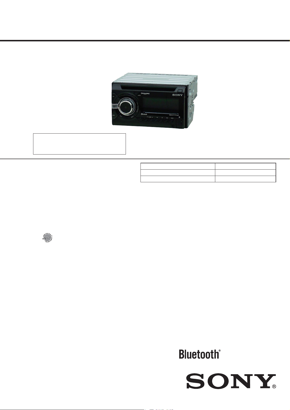
Photo: WX-900BT
The service manual of the mechanism deck, used in
this model, has been issued in a separate volume.
Please refer to the service manual of the MG-101
series for the mechanism deck information.
• The tuner and CD sections have no adjustments.
(US and Canadian models only)
FOR THE CUSTOMERS IN THE USA. NOT
APPLICABLE IN CANADA, INCLUDING IN THE
PROVINCE OF QUEBEC.
POUR LES CLIENTS AUX ÉTATS-UNIS. NON
APPLICABLE AU CANADA, Y COMPRIS LA
PROVINCE DE QUÉBEC.
AUDIO POWER SPECIFICATIONS
CEA2006 Standard
Power Output: 17 Watts RMS × 4 at 4
Ohms < 1% THD+N
SN Ratio: 80 dBA
(reference: 1 Watt into 4 Ohms)
Tuner section (US and Canadian models)
FM
Tuning range: 87.5 – 107.9 MHz
Antenna (aeria l) terminal:
External antenna (aerial) connector
Intermediate frequen cy:
FM CCIR: -1,956.5 to -487.3 kHz and
+500.0 to + 2,095.4 kHz
Usable sensitivity: 8 dBf
Selectivity: 75 dB at 400 kHz
Signal-to-noise ratio: 73 dB
Separation: 50 dB at 1 kHz
Frequency response: 20 – 15,000 Hz
AM
Tuning range: 530 – 1,710 kHz
Antenna (aeria l) terminal:
External antenna (aerial) connector
Sensitivity: 26 μV
Tuner section (AEP and UK models)
FM
Tuning range: 87.5 – 108.0 MHz
Antenna (aeria l) terminal:
External antenna (aer ial) connector
Intermediate frequency:
FM CCIR: -1,956.5 to -487.3 kHz and
+500.0 to +2,095.4 kHz
Usable sensitivity: 8 dBf
Selectivity: 75 dB at 400 kHz
Signal-to-noise ratio: 73 dB
Separation: 50 dB at 1 kHz
Frequency response: 20 – 15,000 Hz
MW/LW
Tuning range:
MW: 531 – 1,602 kHz
LW: 153 – 279 kHz
Antenna (aeria l) terminal:
External antenna (aer ial) connector
Sensitivity: MW: 26 μV, LW: 50 μV
Tuner section
(E, Indian and Australian models)
FM
Tuning range:
87.5 – 108.0 MHz (at 50 kH z step)
87.5 – 108.0 MHz (at 100 kHz step)
87.5 – 107.9 MHz (at 200 kHz step)
FM tuning step:
50 kHz/100 kHz/200 kHz switchable
Antenna (aerial) terminal:
External antenna (aerial) connector
Intermediate frequency:
FM CCIR: -1,956.5 to -487.3 kHz and
+500.0 to +2,095.4 kHz
Usable sensitivity: 8 dBf
Selectivity: 75 dB at 400 kHz
Signal-to-noise ratio: 73 dB
Separation: 50 dB at 1 kHz
Frequency response: 20 – 15,000 Hz
AM
Tuning range:
531 – 1,602 kHz (at 9 kHz step)
530 – 1,710 kHz (at 10 kHz step)
AM tuning step:
9 kHz/10 kHz switchable
Antenna (aerial) terminal:
External antenna (aerial) connector
Sensitivity: 26 μV
Model Name Using Similar Mechanism MEX-N4100BT/N4150BT
Mechanism Type MG-101CF-188
Optical Pick-up Name DAX-25A
SPECIFICATIONS
CD Player section
Signal-to-noise ratio: 120 dB
Frequency response: 10 – 20,000 Hz
Wow and utter: Below measurable limit
The maximum number of: (CD-R/CD-RW only)
–
folders (albums): 150 (including root folder)
–
les (tracks) and folders: 300 (may less than 300
if folder/le nam es contain many
–
displayable characters for a folder/le name: 32
(Joliet)/64 (Romeo)
Corresponding codec: MP3 (.mp3), WMA (.wma)
and AAC (.m4a)
USB Player secti on
Interface: USB (High-speed)
Maximum current: 1 A
The maximum number of recognizable tracks:
10,000
Corresponding codec:
MP3 (.mp3)
Bit rate: 8 - 320 kbps (Supports VBR (Variable
Bit Rate))
Sampling rate: 16 - 48 kHz
WMA (.wma)
Bit rate: 32 - 192 kbps ( Supports VBR
(Variable Bit Rate) )
Sampling rate: 32 kHz, 44.1 kHz, 48 kHz
AAC (.m4a, .mp4)
Bit rate: 8 - 320 kb ps
Sampling rate: 11.025 - 48 kHz
WAV (.w av)
Bit depth: 16 bit
Sampling rate: 44.1 kHz, 48 kHz
FLAC (.ac)
Bit depth: 16 bit, 24 bit
Sampling rate: 44.1 kHz, 48 kHz
characters)
US Model
Canadian Model
WX-850BT/900BT
AEP Model
UK Model
E Model
Australian Model
WX-900BT
Indian Model
WX-900BT/900BTM
Wireless Communication
Communication System:
BLUETOOTH Standard version 3.0
Output:
BLUETOOTH Standard Power Class 2
(Max. +4 dBm)
Maximum communication range:
Line of sight approx. 10 m (33 ft)*
Frequency band:
2.4 GHz band (2.4000 – 2.4835 GHz)
Modulation method: FHSS
Compatible BLUETOOTH Proles*
A2DP (Advanced Audio Distribution Prole) 1.3
AVRCP (Audio Video R emote Control Prole) 1.5
HFP (Handsfree Prole) 1.6
PBAP (Phone Book Access Prole)
SPP (Serial Port Prole)
MAP (Message Access Prole)
HID (Human Interface Device Prole)
Corresponding codec:
SBC (.sbc) and AAC (.m4a)
*1 The actual range will vary depending on factors such
as obstacles between devices, magnetic elds
around a microwave oven , static electricity,
reception sensitivity, antenna (aerial)’s performance,
operating system, software application, etc.
*2 BLUETOOTH standard proles indicate the purpose
of BLUETOOTH communication between devices.
Power amplier section
Output: Speaker outputs
Speaker impedance: 4 – 8 ohms
Maximum power output: 55 W × 4 (at 4 ohms)
– Continued on next page –
1
2
:
AUDIO SYSTEM
9-896-191-02
2016B33-1
2016.02
©
Sony Video & Sound Products Inc.
Published by Sony Techno Create Corporation
Page 2

WX-850BT/900BT/900BTM
T
Ver. 1.1
General
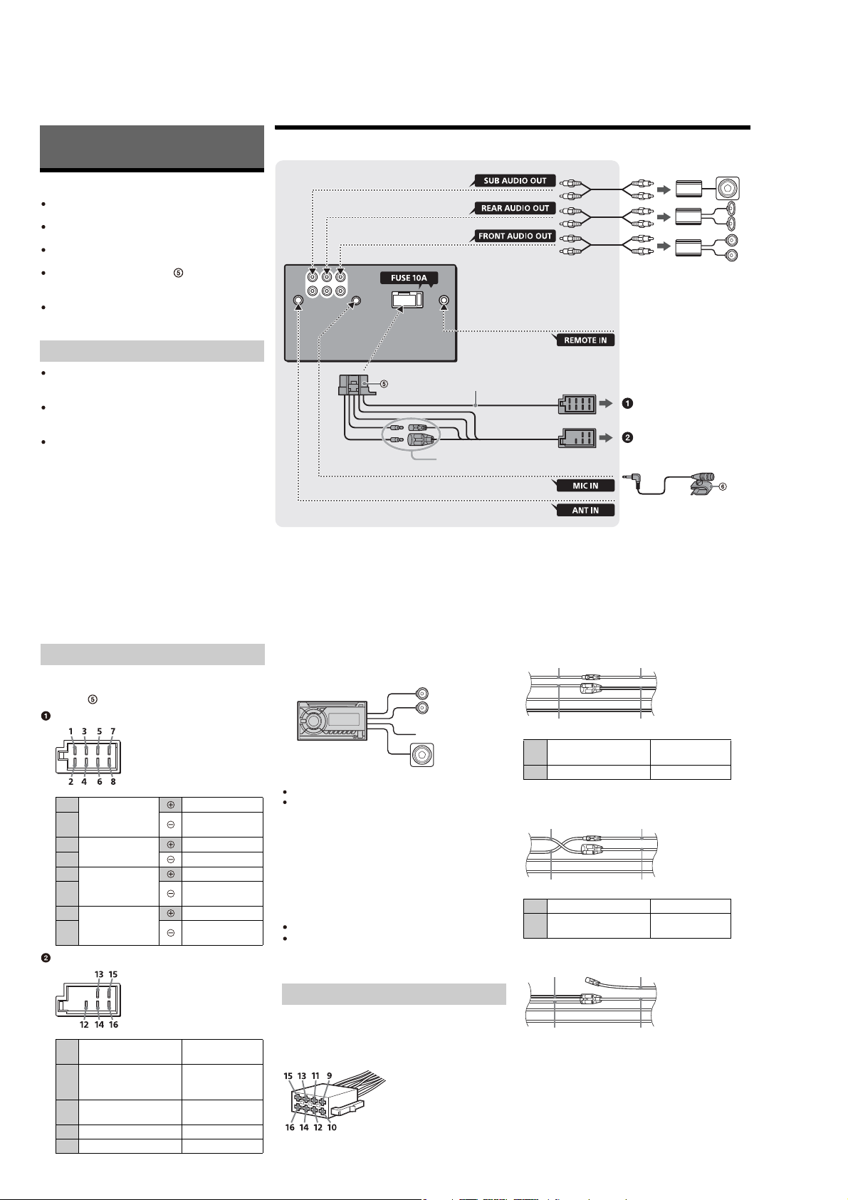
Outputs:
Audio outputs terminal: front, rear, sub
Power antenna (aerial)/Power amplier control
terminal (REM OUT )
Inputs:
SiriusXM input terminal (900BT: US and Canadian models only)
Remote controller input terminal
Antenna (aerial) input terminal
MIC input termin al
AUX input jack (stereo mini jack)
USB port
Power requirements: 12 V DC car battery (negative
ground (earth))
Rated current consumptio n: 10 A
Dimensions:
Approx. 178 mm × 100 mm × 178 mm
1
(7
/ 8 in × 4 in × 7 1/ 8 in) (w/h/d)
Mounting dimensions:
Approx. 182 mm × 111 mm × 159 mm
1
(7
/4 in × 4 3/ 8 in × 6 3/ 8 in) (w/h/d)
Mass: Approx. 1.4 kg (3 lb 2 oz)
Package contents:
Main unit (1)
Remote commander (1): RM-X231 (US, Canadian, E, Indian
and Australian models only)
Microphone (1)
Parts for installation and connections (1 set)
Design and specications are subject to change
without notice.
Copyrights
SiriusXM Connect Vehicle Tuner and Subscription
sold separately.
www.siriusxm.com
Sirius, XM and all related marks and logos are
trademarks of Sirius XM Radio Inc. All rights
reserv ed.
The Bluetooth® word mark and logos are registered
trademarks owned by Bluetooth SIG, Inc. and any
use of such marks by Sony Corporation is under
license. Other trademarks and trade names are
those of their respective owners.
The N-Mark is a trademark or registered trademark
of NFC Forum, Inc. in the United States and in other
countries.
Windows Media is either a registered trademark or
trademark of Microsoft Corporation in the United
States and/or other count ries.
This product is protected by certain intellectual
property rights of Microsoft Corporation. Use or
distribution of such technology outside of this
product is prohibited without a license from
Microsoft or an authorized Microsoft subsidiary.
iPhone, iPod, iPod classic, iPod nano, iPod touch,
and Siri are trademarks of Apple Inc., registered in
the U.S. and other countries. App Store is a service
mark of Apple Inc.
MPEG Layer-3 audio coding technology and patents
licensed from Fraunhofer IIS and Thomson.
Pandora®, the Pandora® logo, and the Pandora®
trade dress are trademarks or registered
trademarks of Pandora Media, Inc., used with
permission.
Google, Google Play and Android are trademarks of
Google Inc.
libFLAC
Copyright (C) 2000-2009 Josh Coalson
Copyright (C) 2011-2013 Xiph.Org Foundation
Redistribution and use in source and binary forms,
with or without modication, are permitted
provided that the following conditions are met:
Redistributions of source code must retain the –
above copyright notice, this l ist of conditions and
the following disc laimer.
–
Redistributions in binary form must reproduce
the above copyright notice, this list of conditions
and the followin g disclaimer in the
documentation and/or other materials provided
with the distribution.
–
Neither the name of the Xiph.org Foundation nor
the names of i ts contributors may be us ed to
endorse or promote products derived from this
software without specic prior written
permission.
THIS SOFTWARE IS PROVIDED BY THE COPYRIG HT
HOLDERS AND CONTRIBUTORS “AS IS” AND ANY
EXPRESS OR IMPLIED WARRANTI ES, INCLUDING,
BUT NOT LIMITED TO, THE IMPLIED WARRANTIES OF
MERCHANTABILITY AND FITNESS FOR A
PARTICULAR PURPOSE ARE DISCLAIMED. IN NO
EVENT SHALL THE FOUNDATION OR CONTRIBUTORS
BE LIABLE FOR ANY DIRECT, INDIRECT, INCIDENTAL,
SPECIAL, EXEMPLARY, OR CONSEQUENTIAL
DAMAGES (INCLUDING, BUT NOT LIMITED TO,
PROCUREMENT OF SUBSTITUTE GOODS OR
SERVICES; LOSS OF USE, DATA, OR PROFITS; OR
BUSINESS INTERRUPTION) HOWEVE R CAUSED AND
ON ANY THEORY OF LIABILITY, WHETHER IN
CONTRACT, STRICT LIABILITY, OR TORT (INCLUDING
NEGLIGENCE OR OTHERWISE) ARISING IN ANY WAY
OUT OF THE USE OF THIS SOFTWARE, EVEN IF
ADVISED OF THE POSSIB ILITY OF SUCH DAMAGE.
NOTES ON CHIP COMPONENT REPLACEMENT
• Never reuse a disconnected chip component.
• Notice that the minus side of a tantalum capacitor may be dam-
aged by heat.
FLEXIBLE CIRCUIT BOARD REPAIRING
• Keep the temperature of soldering iron around 270 °C during
repairing.
• Do not touch the soldering iron on the same conductor of the
circuit board (within 3 times).
• Be careful not to apply force on the conductor when soldering
or unsoldering.
US and Canadian models:
CAUTION
he use of optical instruments with this product will
increase eye hazard.
CAUTION
Use of controls or adjustments or performance of procedures
other than those specifi ed herein may result in hazardous radia-
tion exposure.
2
SAFETY-RELATED COMPONENT WARNING!
COMPONENTS IDENTIFIED BY MARK 0 OR DOTTED LINE
WITH MARK 0 ON THE SCHEMATIC DIAGRAMS AND IN
THE PARTS LIST ARE CRITICAL TO SAFE OPERATION.
REPLACE THESE COMPONENTS WITH SONY PARTS
WHOSE PART NUMBERS APPEAR AS SHOWN IN THIS
MANUAL OR IN SUPPLEMENTS PUBLISHED BY SONY.
ATTENTION AU COMPOSANT AYANT RAPPORT
À LA SÉCURITÉ!
LES COMPOSANTS IDENTIFIÉS PAR UNE MARQUE 0 SUR
LES DIAGRAMMES SCHÉMATIQUES ET LA LISTE DES
PIÈCES SONT CRITIQUES POUR LA SÉCURITÉ DE FONCTIONNEMENT. NE REMPLACER CES COMPOSANTS QUE
PAR DES PIÈCES SONY DONT LES NUMÉROS SONT DONNÉS DANS CE MANUEL OU DANS LES SUPPLÉMENTS
PUBLIÉS PAR SONY.
Page 3
WX-850BT/900BT/900BTM
SECTION 1
SERVICING NOTES
TABLE OF CONTENTS
1. SERVICING NOTES ............................................. 3
2. GENERAL .................................................................. 16
3. DISASSEMBLY
3-1. Disassembly Flow ........................................................... 22
3-2. Mini Fuse (Blade Type) (FU1), Cover ............................ 22
3-3. Panel Front Block ........................................................... 23
3-4. CD Mechanism Deck (MG-101CF-188) ........................ 24
3-5. MAIN Board ................................................................... 25
3-6. Knob (VOL) Assy (NFC1), Panel Front Assy,
KEY Board ...................................................................... 26
3-7. Service Position .............................................................. 27
4. TEST MODE ............................................................ 27
5. DIAGRAMS
5-1. Block Diagram - SERVO/USB/Bluetooth Section - ....... 28
5-2. Block Diagram - MAIN Section - ................................... 29
5-3. Block Diagram
- PANEL/POWER SUPPLY Section - ............................ 30
5-4. Printed Wiring Boards - MAIN Section (1/2) - .............. 32
5-5. Printed Wiring Board - MAIN Section (2/2) - ................ 33
5-6. Schematic Diagram - MAIN Section (1/4) - ................... 34
5-7. Schematic Diagram - MAIN Section (2/4) - ................... 35
5-8. Schematic Diagram - MAIN Section (3/4) - ................... 36
5-9. Schematic Diagram - MAIN Section (4/4) - ................... 37
5-10. Printed Wiring Board
- KEY Board (Component Side) -................................... 38
5-11. Printed Wiring Board
- KEY Board (Conductor Side) - .................................... 39
5-12. Schematic Diagram - KEY Board - ................................ 40
The SERVICING NOTES contains important information for
servicing. Be sure to read this section before repairing the
unit.
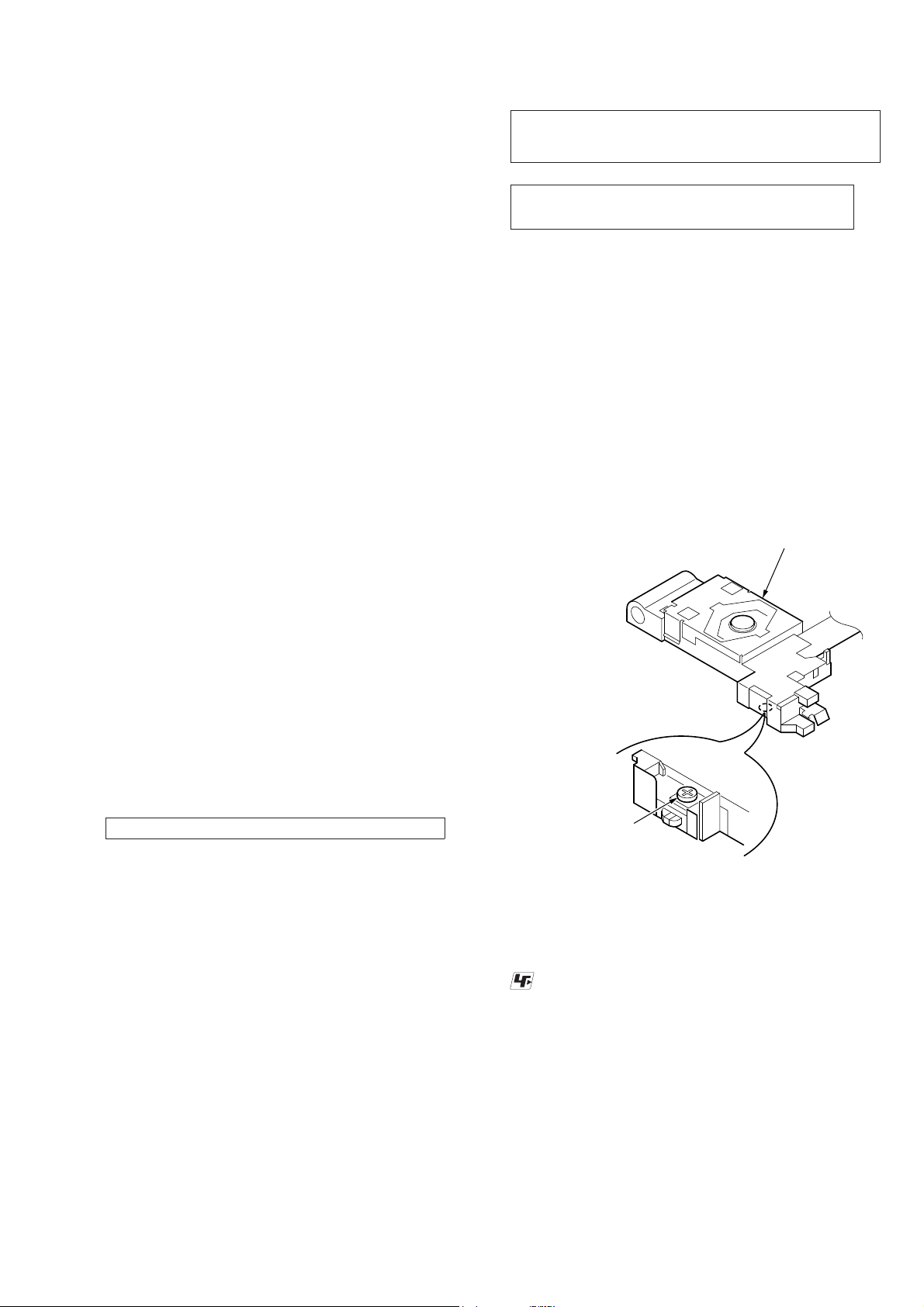
NOTES ON HANDLING THE OPTICAL PICK-UP
BLOCK OR BASE UNIT
The laser diode in the optical pick-up block may suffer electrostatic break-down because of the potential difference generated by
the charged electrostatic load, etc. on clothing and the human body.
During repair, pay attention to electrostatic break-down and also
use the procedure in the printed matter which is included in the
repair parts.
The fl exible board is easily damaged and should be handled with
care.
NOTES ON LASER DIODE EMISSION CHECK
Never look into the laser diode emission from right above when
checking it for adjustment. It is feared that you will lose your sight.
If the optical pick-up block is defective, please replace the whole
optical pick-up block.
Never turn the semi-fi xed resistor located at the side of optical
pick-up block.
optical pick-up
6. EXPLODED VIEWS
6-1. Main Section ................................................................... 49
6-2. Front Panel Section ......................................................... 50
7. ELECTRICAL PARTS LIST .............................. 51
Accessories are given in the last of the electrical parts list.
semi-fixed resistor
UNLEADED SOLDER
Boards requiring use of unleaded solder are printed with the leadfree mark (LF) indicating the solder contains no lead.
(Caution: Some printed circuit boards may not come printed with
the lead free mark due to their particular size)
: LEAD FREE MARK
Unleaded solder has the following characteristics.
• Unleaded solder melts at a temperature about 40 °C higher
than ordinary solder.
Ordinary soldering irons can be used but the iron tip has to be
applied to the solder joint for a slightly longer time.
Soldering irons using a temperature regulator should be set to
about 350 °C.
Caution: The printed pattern (copper foil) may peel away if
the heated tip is applied for too long, so be careful!
• Strong viscosity
Unleaded solder is more viscous (sticky, less prone to fl ow)
than ordinary solder so use caution not to let solder bridges
occur such as on IC pins, etc.
• Usable with ordinary solder
It is best to use only unleaded solder but unleaded solder may
also be added to ordinary solder.
3
Page 4
WX-850BT/900BT/900BTM
+ side up
Ver. 1.1
REPLACING THE LITHIUM BATTERY OF THE REMOTE
COMMANDER (850BT, 900BT: US, Canadian, E, Indian,
Australian models and 900BTM only)
Under normal conditions, the battery will last
approximately 1 year. (The service life may be
shorter, depending on the conditions of use.)
When the battery becomes weak, the range of the
remote commander becomes shorter.
CAUTION
Danger of explosion if battery is incorrectly
replaced. Replaced only with the same or
equivalent type.
Notes on the lithium battery
ˎ Keep the lithium battery out of the reach of children.
Should the battery be swallowed, immediately
consult a doctor.
ˎ Wipe the battery with a dry cloth to ensure a good
contact.
ˎ Be sure to observe the correct polarity when installing
the battery.
ˎ Do not hold the battery with metallic tweezers,
otherwise a short-circuit may occur.
WARNING
Battery may explode if mistreated.
Do not recharge, disassemble, or dispose of in
fire.
MODEL IDENTIFICATION
Distinguish by Part No. on the bottom side of the main unit.
– Bottom view –
(US, Canadinan, AEP and UK models)
Model Number Label
Part No.
– Bottom view –
(E, Indian and Australian models)
Model Number Label
Part No.
Part No. Model
4-575-528-0[]
4-575-529-0[]
4-575-530-0[]
4-575-531-0[]
4-575-532-0[]
4-588-101-0[]
WX-900BT: US and Canadian models (UC)
WX-900BT: AEP and UK models (EUR)
WX-900BT: E and Australian models (E)
WX-900BT: Indian model (IN)
WX-900BTM: Indian model
(MARUTI SUZUKI model) (IN)
WX-850BT: US and Canadian models
(Wal-Mart model) (UC)
DESTINATION ABBREVIATIONS
The following abbreviations for model destinations are used in this
service manual.
• Abbreviations
AUS : Australian model
CND : Canadian model
IND : Indian model
4
Page 5
WX-850BT/900BT/900BTM
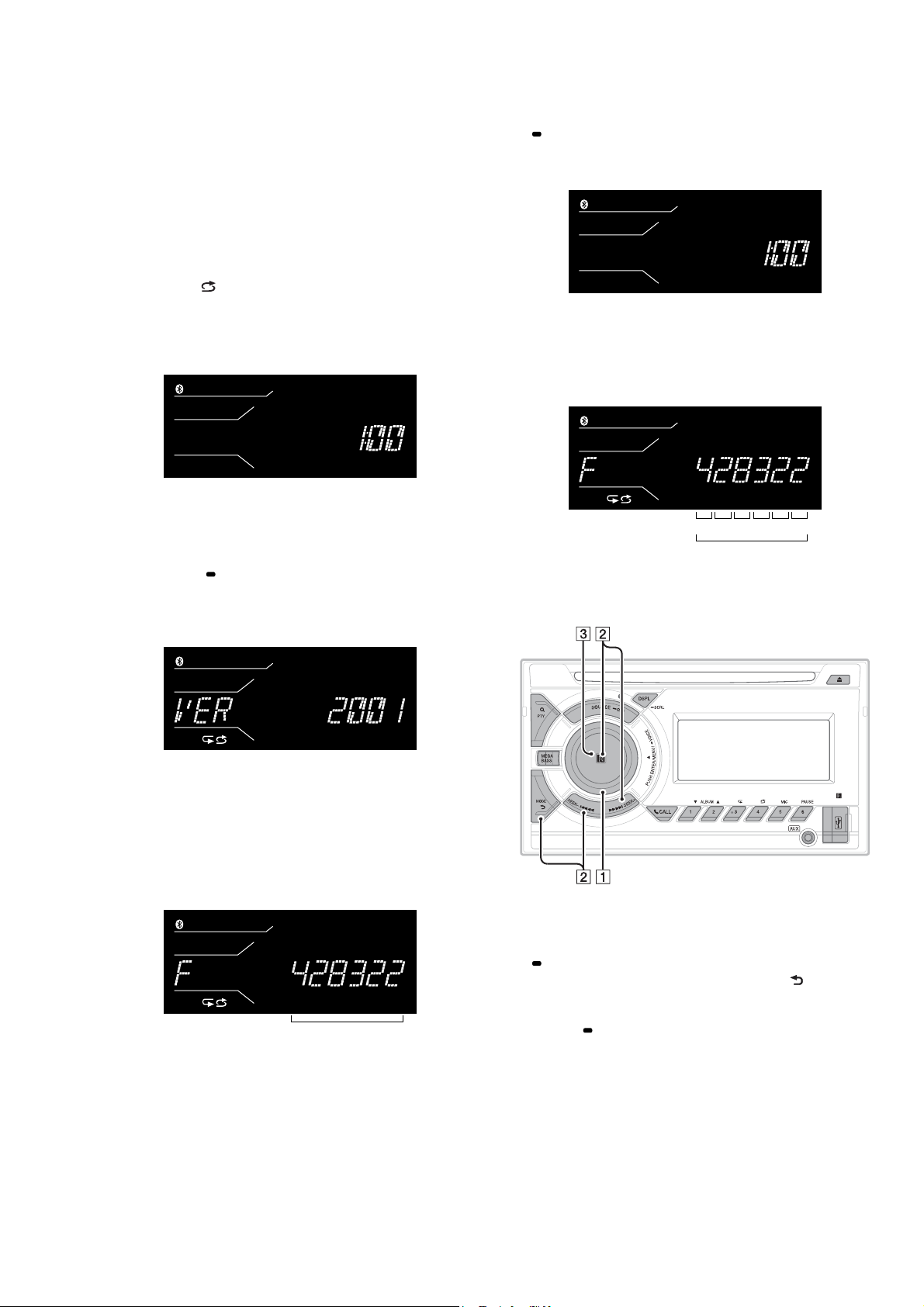
DESTINATION SETTING METHOD
When the complete MAIN board or serial fl ash (IC502) is re-
placed, the destination setting is necessary.
1. Destination Setting
Set destination according to the procedure below.
1-1. Setting the Destination Code
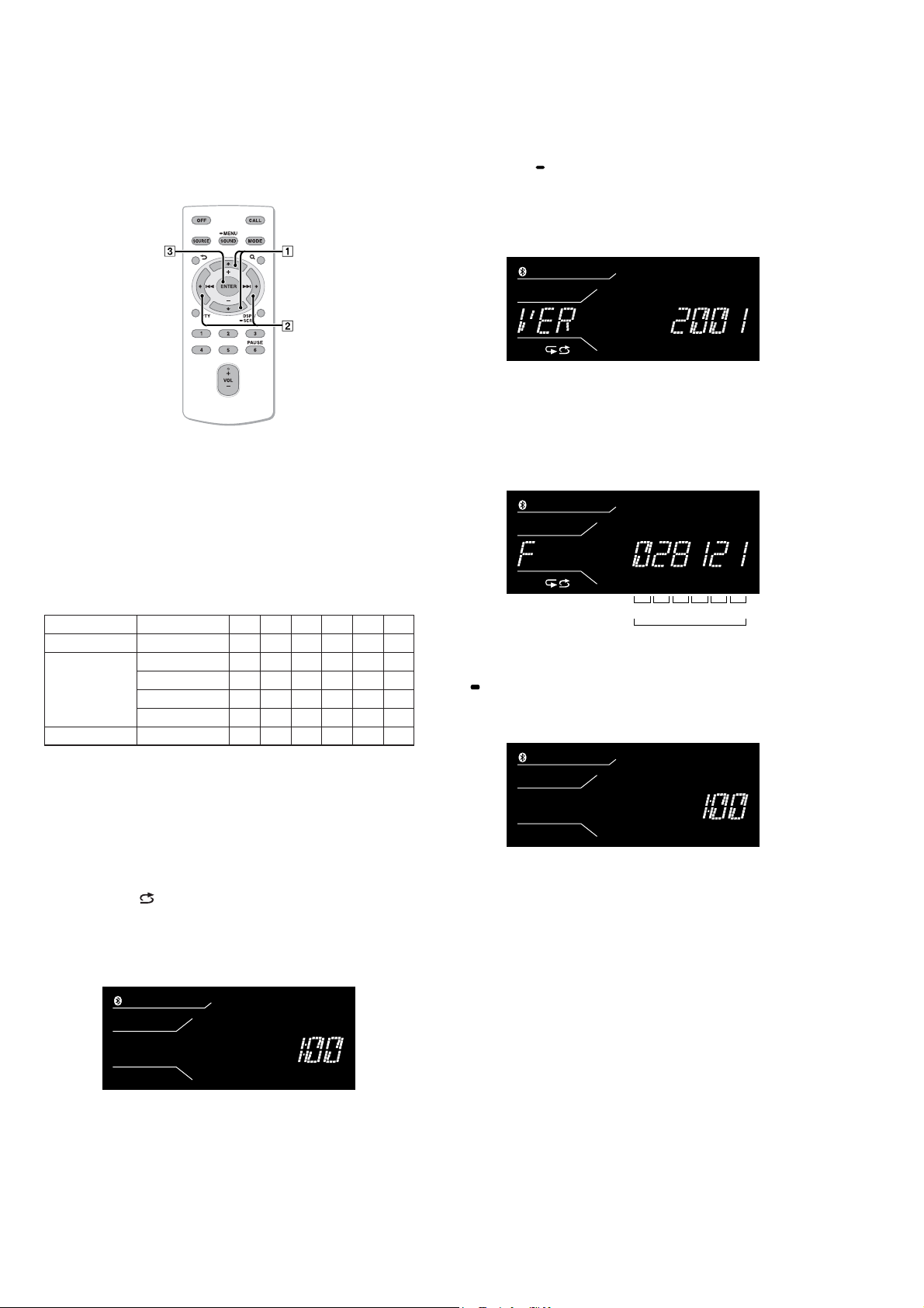
1. In the state of source off (the clock is displayed on the liquid
crystal display), enter the test mode by pressing the buttons in
order of the [ 4] t [MIC 5] t [PAUSE 6] (press only the
[PAUSE 6] button for two seconds).
(Displayed characters/values in the following fi gure are ex-
ample)
Clock display
2. In the state in which the software main version is displayed on
the liquid crystal display (refer to the following fi gure), enter
the destination setting mode by pressing the buttons in order of
the [M> SEEK+] t [SEEK– .m] t [v PUSH ENTER/MENU/ VOICE].
(Displayed characters/values in the following fi gure are ex-
ample)
4. The resetting operation is executed by pressing the [SOURCE
OFF] button for 1 second after the setting ends, and the unit
returns to the normal condition.
Display after reset
1-2. Display in Destination Setting Mode
Note: The displayed contents of the following fi gure is an example. The
destination code is different depending on the destination of the
product.
Destination code
OP0OP1OP2OP3OP4OP5
6 digits
1-3. Entering the Destination Code
• Method of operation by main unit
Software main version
3. Input the alphanumeric character of 6 digits displayed on the
liquid crystal display, and execute the destination setting.
Note 1: The displayed contents of the following fi gure is an example. The
destination code is different depending on the destination of the
product.
Note 2: Refer to the following “1-3. Entering the Destination Code” for
operation method.
Destination code
6 digits
1. Rotate the control dial, and select the alphanumeric character
of “0 to F”.
2. The digit advances by pressing the [v PUSH ENTER/MENU/
VOICE] or [M> SEEK+] button.
The digit returns by pressing the [MODE ] or [SEEK–
.m] button.
3. The setting is completed by pressing the [v PUSH ENTER/
MENU/ VOICE] button at the state of cursor position of
“OP0”, then the display turns off, the initialization operation
is done, and the display returns to the clock display.
– Continued on next page –
5
Page 6
WX-850BT/900BT/900BTM
Ver. 1.1
• Method of operation by remote commander
(850BT, 900BT: US, Canadian, E, Indian, Australian
models and 900BTM only)
Note: The model to which the remote commander is not attached can
also be operated by using the remote commander.
1. Press the [V] or [v] button, and select the alphanumeric character of “0 to F”.
2. The digit advances by pressing the [b] or [ENTER] button.
The digit returns by pressing the [B] button.
3. The setting is completed by pressing the [ENTER] button at
the state of cursor position of “OP0”, then the display turns off,
the initialization operation is done, and the display returns to
the clock display.
2. In the state in which the software main version is displayed
on the liquid crystal display (refer to the following fi gure),
enter the destination setting value display mode by pressing
the [DSPL
SCRL] button twice (software main version t
Bluetooth address t destination code).
(Displayed characters/values in the following fi gure are ex-
ample)
Software main version
3. Confi rm the alphanumeric character of 6 digits on the liquid
crystal display is a value correctly input.
Note: The displayed contents of the following fi gure is an example. The
destination code is different depending on the destination of the
product.
Destination code
1-4. Destination Code
Model Destination OP5 OP4 OP3 OP2 OP1 OP0
WX-850BT US, Canadian 4 2 8 1 4 2
US, Canadian 4 2 8 3 2 2
WX-900BT
WX-900BTM Indian 0 6 9 1 3 0
AEP, UK 0 2 8 1 2 1
E, Australian 0 6 B 1 2 0
Indian 0 6 9 1 2 0
2. Confi rmation After Destination Setting
Execute the following operation after completing the destination
setting, and confi rm a correct destination was set.
Destination setting checking method:
1. In the state of source off (the clock is displayed on the liquid
crystal display), enter the test mode by pressing the buttons in
order of the [ 4] t [MIC 5] t [PAUSE 6] (press only the
[PAUSE 6] button for two seconds).
(Displayed characters/values in the following fi gure are ex-
ample)
Clock display
OP0OP1OP2OP3OP4OP5
6 digits
4. The resetting operation is executed by pressing the [SOURCE
OFF] button for 1 second after the confi rming ends, and the
unit returns to the normal condition.
Display after reset
6
Page 7
WX-850BT/900BT/900BTM
TEST DISCS
Use following TEST DISC (for CD) when this unit confi rms the
operation and checks it.
Part No. Description
3-702-101-01 DISC (YEDS-18), TEST
4-225-203-01 DISC (PATD-012), TEST
NOTE OF PERFORMING THE OPERATION CHECK
When performing the operation check in the state that is removed
the CD mechanism deck from the main unit, it is necessary to use
a long fl exible fl at cable.
When performing the operation check, use following fl exible fl at
cable.
Part No. Description
1-846-819-31 CABLE FLEXIBLE FLAT (27 CORE)
(Length: 150 mm)
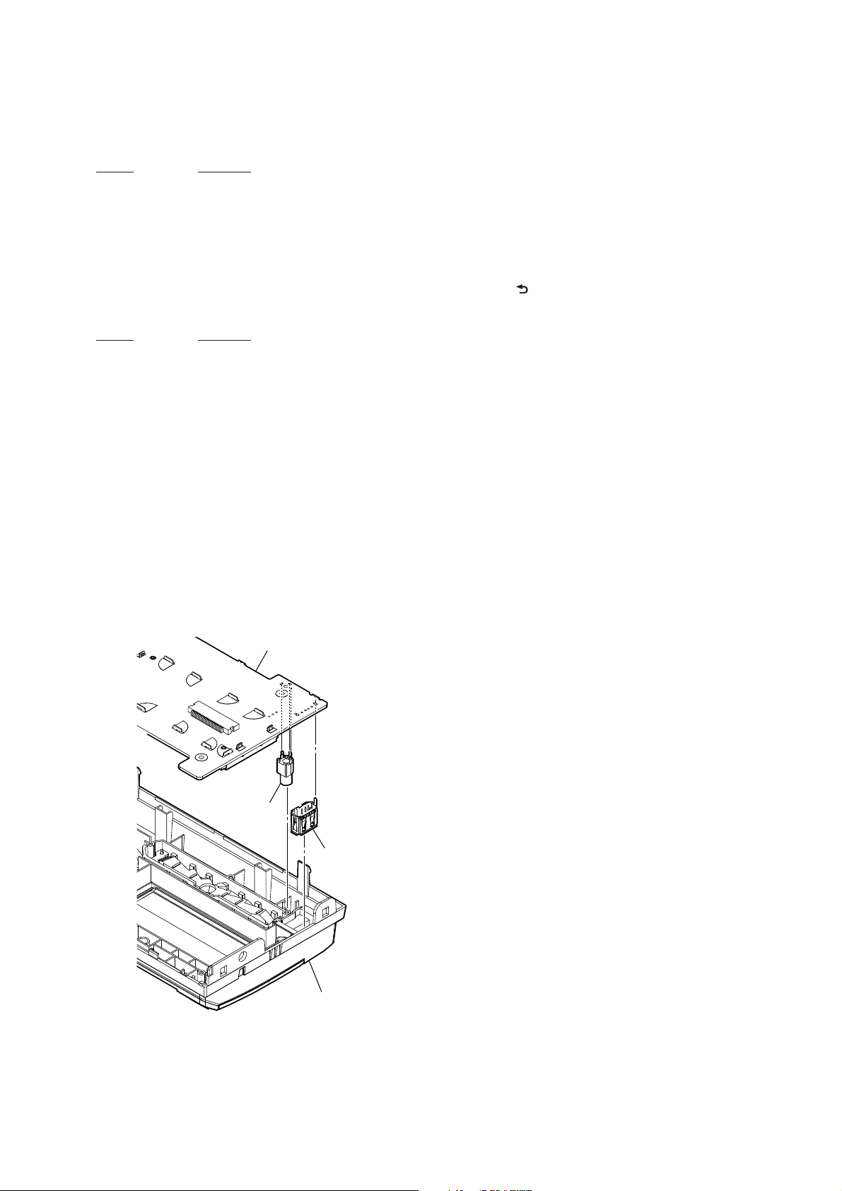
NOTE OF REPLACING THE ANT001, IC001, IC503,
IC804, IC1002 AND IC1009 ON THE MAIN BOARD
ANT001, IC001, IC503, IC804, IC1002 and IC1009 on the MAIN
board cannot replace with single. When these parts are damaged,
replace the complete mounted board.
NOTE FOR REPLACING OF THE USB CONNECTOR
(CN902) AND THE AUX JACK (J901)
To replace the USB connector and AUX jack requires alignment.
1. Insert the USB connector and AUX jack into the front panel.
2. Place the KEY board on the front panel and align the terminals
of the USB connector and AUX jack with the holes in the KEY
board.
3. Solder six terminals of the USB connector and three terminals
of the AUX jack.
CANCELING THE DEMO MODE
You can cancel the demonstration display which
appears when the source is off and the clock is
displayed.
1 Press MENU, rotate the control dial to
select [SET GENERAL], then press it.
2 Rotate the control dial to select [SET
DEMO], then press it.
3 Rotate the control dial to select [SET
DEMO-OFF], then press it.
The setting is complete.
4 Press (back) twice.
The display returns to normal reception/play
mode.
KEY board
AUX jack
(J901)
USB connector
(CN902)
front panel
7
Page 8
WX-850BT/900BT/900BTM
BLUETOOTH FUNCTION CHECKING METHOD USING
A SMARTPHONE OR CELLULAR PHONE
1. Required Equipment
• This unit to be tested, external microphone of attachment
• Bluetooth compatible smartphone or cellular phone
• Bluetooth audio devices (SONY NWZ-A826, or select from
connectable smartphone, cellular phones or audio devices list)
• Speaker connection (at least Front L/R ch)
• DC power supply (12 V)
2. Preparation
• Confi rm the setting of this unit and note down it.
• Press the [
CALL] button and rotate the control dial until
“SET PAIRING” appears, then press it, confi rm that the Blue-
tooth signal icon ( ) is fl ashing.
• Turn on the Bluetooth function of the smartphone or cellular
phone.
3. Test Environment
• No other Bluetooth device is making a communication in the
periphery (within 20 m).
• No other this unit are supplied with electric power.
• There are no two or more wireless LAN access points in the
periphery (with 50 m) (one is OK).
• The set should be tested in a place such as a meeting room, free
from ambient noise.
• The speaker at the far end should be in a place such as another
meeting room separated acoustically.
4. Setting
Install this unit on the desktop.
Approx. 50 cm
Speaker
Unit
6. Bluetooth Phone (Hands Free) Function Check
1. Search for this unit from the Bluetooth device (smartphone or
cellular phone), and confi rm whether this unit (model name) is
displayed.
2. Search for the distance of this unit and the Bluetooth device
(smartphone or cellular phone) about 5 m apart.
Confi rm whether the this unit is displayed after it searches.
3. Do the pairing of the smartphone or cellular phone and this
unit.
(If the input of the passkey is required, to enter the “0000”)
4. Connect the smartphone or cellular phone with this unit, and
confi rm the “HF” icon (
) is lights.
5. Confi rm the connection continues even if the distance of the
smartphone or cellular phone and this unit is separated by
about 5 m.
6. Set this unit except the “BT PHONE” source, and call the
smartphone or cellular phone connected with this unit.
Confi rm the automatic change of this unit into “BT PHONE”
source, and the change into the screen for incoming calls.
Confi rm the ring tone is heard from the front speaker.
7. Take a phone call (press the [ CALL] button), and start a
conversation.
Confi rm the other person voice is heard from the speaker.
Speak toward an external microphone at the following condi-
tion, and confi rm the other party hears its voice (An external
microphone is connected).
Compare the sound quality with a normal set. Confi rm that
there is no big difference.
8. Turn on ACC from off, and confi rm whether this unit connects
Bluetooth with the smartphone or cellular phone again.
Note: Depending on the smartphone or cellular phone, it might not recon-
nect automatically when ACC is turned on.
7. Bluetooth Audio Function Check
Note 1: Depending on the connecting BT Audio device, track information
If the device doesn’t support AVRCP1.3, or, if AVRCP1.3 feature
Even if there is no track information on display during playback
(e.g. track name, playback time) can be on display.
of the device has not been validated with this unit, the track information won’t be shown.
of an AVRCP1.3 device, it is not a failure of this unit.
Approx. 80 cm
Teste r
5. Precautions
Beware of the following points when conducting the
talking test:
• There is no fault if a talking can be made by adjusting appropriately the volume of the telephone of the other party and
the smartphone or cellular phone connected through the Bluetooth, besides the setup of this unit.
• The speaker’s voice will become loud naturally if the periphery is noisy, or become low if quiet (even though the speaker
intents to talk on the same volume level).
• The speaker’s voice will become loud naturally if the other
party’s voice is loud.
1. Connect the Bluetooth audio device (or smartphone, cellular
phone with Bluetooth audio function) with this unit, and confi rm the “Audio Streaming” icon ( ) is lights.
2. Playback the Bluetooth audio. Confi rm the sound is emitted
from this unit when this unit is switched to “BT AUDIO”
source.
3. Confi rm whether Bluetooth audio can be controlled by oper-
ating this unit (the [M > SEEK+], [SEEK– . m] and
[PAUSE 6] buttons operation).
Note 2: Varies depending on the connected Bluetooth audio device.
8. What to Do after Checking
• After checking, this unit to execute initialization (refer to “IMPORTANT NOTE OF INITIALIZING” on page 15).
(Connected device information is deleted)
8
Page 9
WX-850BT/900BT/900BTM
–
BLUETOOTH INFORMATION WRITING METHOD
When the complete MAIN board or knob (VOL) assy (Ref. No.
NFC1) is replaced, the writing of Bluetooth information is necessary.
Write the Bluetooth information according to the procedure below.
Preparation:
• Windows PC
• NFC compatible smartphone that installed the fi le manager ap-
plication (ASTRO File Manager, File Expert, etc.)
• USB cable for the smartphone
• NFC Tag Data Writing Application
(Application name: NFCtagWriter_gm.apk)
Note: Confi rm the method of obtaining the NFC Tag Data Writing Ap-
plication and its latest version with the each service headquarters.
Notes on the use of the NFC Tag Data Writing Application
• The NFC Tag Data Writing Application is updated on an irregular basis.
Always use the latest version of the NFC Tag Data Writing
Application.
To confi rm the version of the NFC Tag Data Writing Appli-
cation, refer to “Checking the Version of the NFC Tag Data
Writing Application” on page 10.
• Be sure to uninstall older versions of the NFC Tag Data
Writing Application before installing the latest version.
• There are multiple types of the NFC Tag Data Writing Application. If multiple NFC Tag Data Writing Applications
are installed on a smartphone, do not launch more than one
at the same time.
• The NFC Tag Data Writing Application varies depending on
your model.
Be sure to use the NFC Tag Data Writing Application that
supports your model.
Use of NFC Tag Data Writing Applications that do not sup-
port your model is strictly prohibited.
1. Installing the NFC Tag Data Writing Application for
the Servicing
Install the NFC Tag Data Writing Application on the smart-
phone for writing of Bluetooth information.
If the NFC Tag Data Writing Application is already installed,
confi rm the following.
• Be absolutely sure that the NFC Tag Data Writing Application supports your model.
• Confi rm that the NFC Tag Data Writing Application is
the latest version.
(Refer to “Checking the Version of the NFC Tag Data
Writing Application” on page 10)
Procedure:
1. Prepare the NFC Tag Data Writing Application on the PC.
Note: Be absolutely sure that the NFC Tag Data Writing Application sup-
ports your model.
2. Connect the smartphone to the PC with the USB cable.
3. Transfer the NFC Tag Data Writing Application to the smartphone.
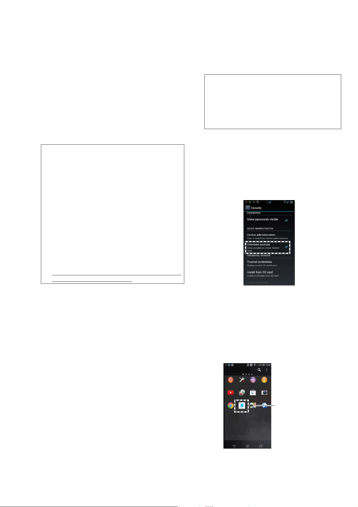
4. When tapping the “Settings” → “Security” on the screen of the
smartphone, check the box “Unknown sources”.
5. Disconnect the smartphone from the PC.
6. Use the fi le manager application to explore the NFC Tag Data
Writing Application on the smartphone.
7. Click on the NFC Tag Data Writing Application to open
it, and install the NFC Tag Data Writing Application to the
smartphone.
8. When tapping the “Settings” → “Security” on the screen of the
smartphone, uncheck the box “Unknown sources”.
Screen after the installation
for reference –
Movies
Settings AlbumWALKMAN
YouTube Camera
Media Player
Play Store
NFC Tag Data
Chrome NFCtagWriter
Browser
Maps
Writing Application
9. Refer to “Checking the Version of the NFC Tag Data Writing
Application” on page 10, and confi rm that the NFC T
ag Data
Writing Application is the latest version.
9
Page 10
WX-850BT/900BT/900BTM
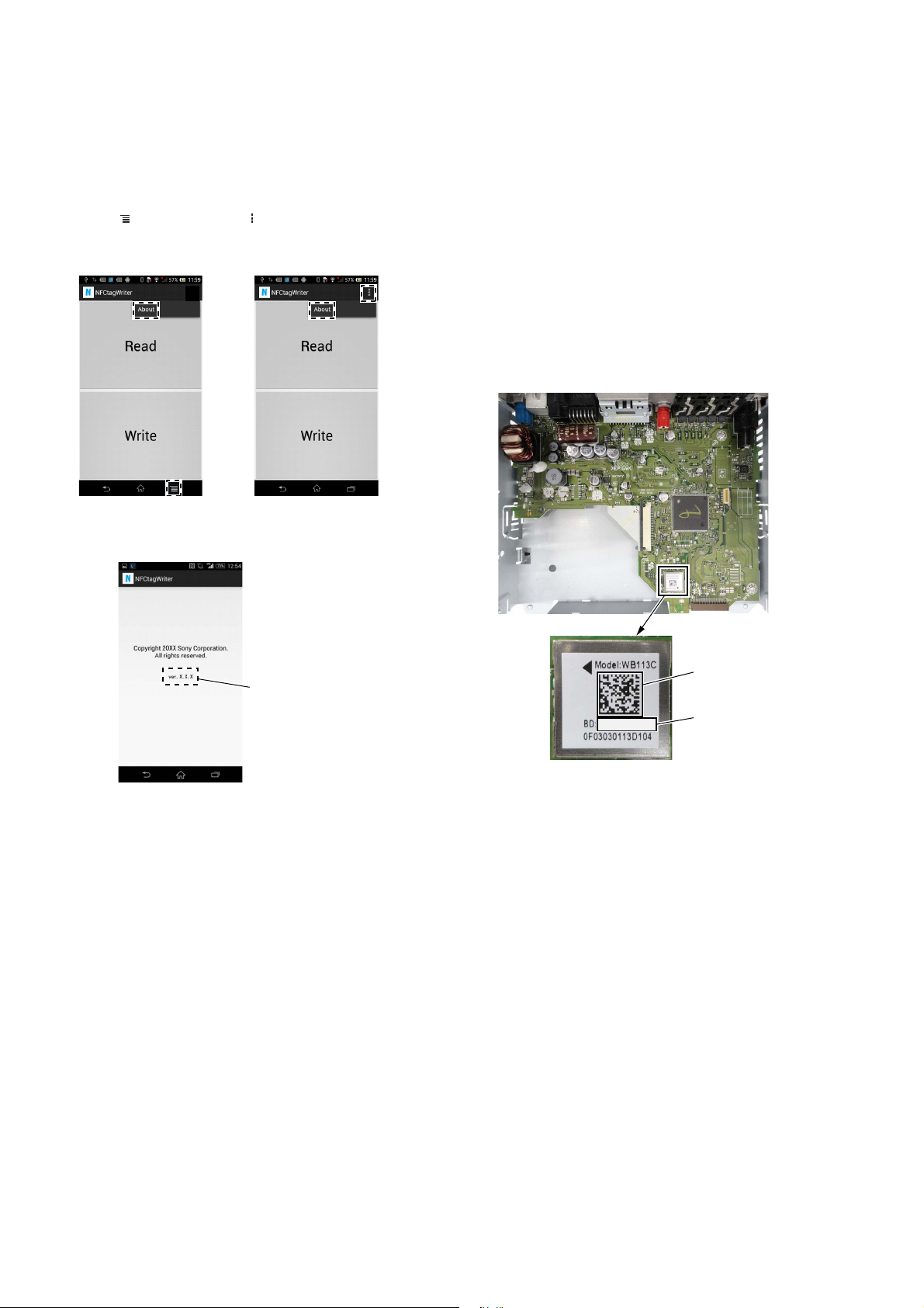
• Checking the Version of the NFC Tag Data Writing
Application
Procedure:
1. Start the NFC Tag Data Writing Application on the smartphone.
2. Tap the “ ” (menu button) or “ ” of the screen of the smartphone, then tap the “About” that is displayed on the screen of
the smartphone.
or
3. Check that version of the NFC Tag Data Writing Application
for the servicing is displayed on the screen of the smartphone.
2. Writing the NFC Tag Data
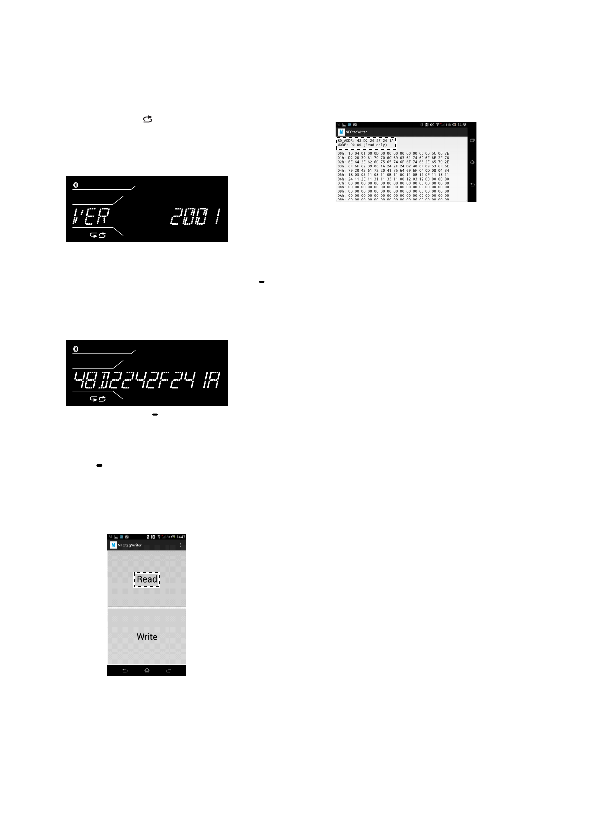
Write the NFC tag data (Bluetooth information) to the NFC module in the knob (VOL) assy (Ref. No. NFC1).
Procedure:
1. Check the Bluetooth address (BD_ADDR).
There are following two checking methods.
• How to read from the BT module label
• How to display on the liquid crystal display by the test
mode
How to read from the BT module label:
Set the unit to the state where the BT module on the MAIN
board can be seen.
(Refer to “3. DISASSEMBLY” on
page 22 and after)
– MAIN Board (Component Side) –
Here version is
displayed
48D2242F241A
BT module label
BD_ADDR
(Barcode)
BD_ADDR
– Continued on next page –
10
Page 11
WX-850BT/900BT/900BTM
How to display on the liquid crystal display by the
test mode:
1 In the state of source off (the clock is displayed on the
liquid crystal display), enter the test mode by pressing the
buttons in order of the [ 4] t [MIC 5] t [PAUSE 6]
(press only the [PAUSE 6] button for two seconds).
(Displayed characters/values in the following fi gure are
example)
Software main version
2 In the state in which the software main version is displayed
on the liquid crystal display, enter the Bluetooth address
(BD_ADDR) display mode by pressing the [DSPL
SCRL] button.
(Displayed characters/values in the following fi gure are
example)
Bluetooth address (BD_ADDR)
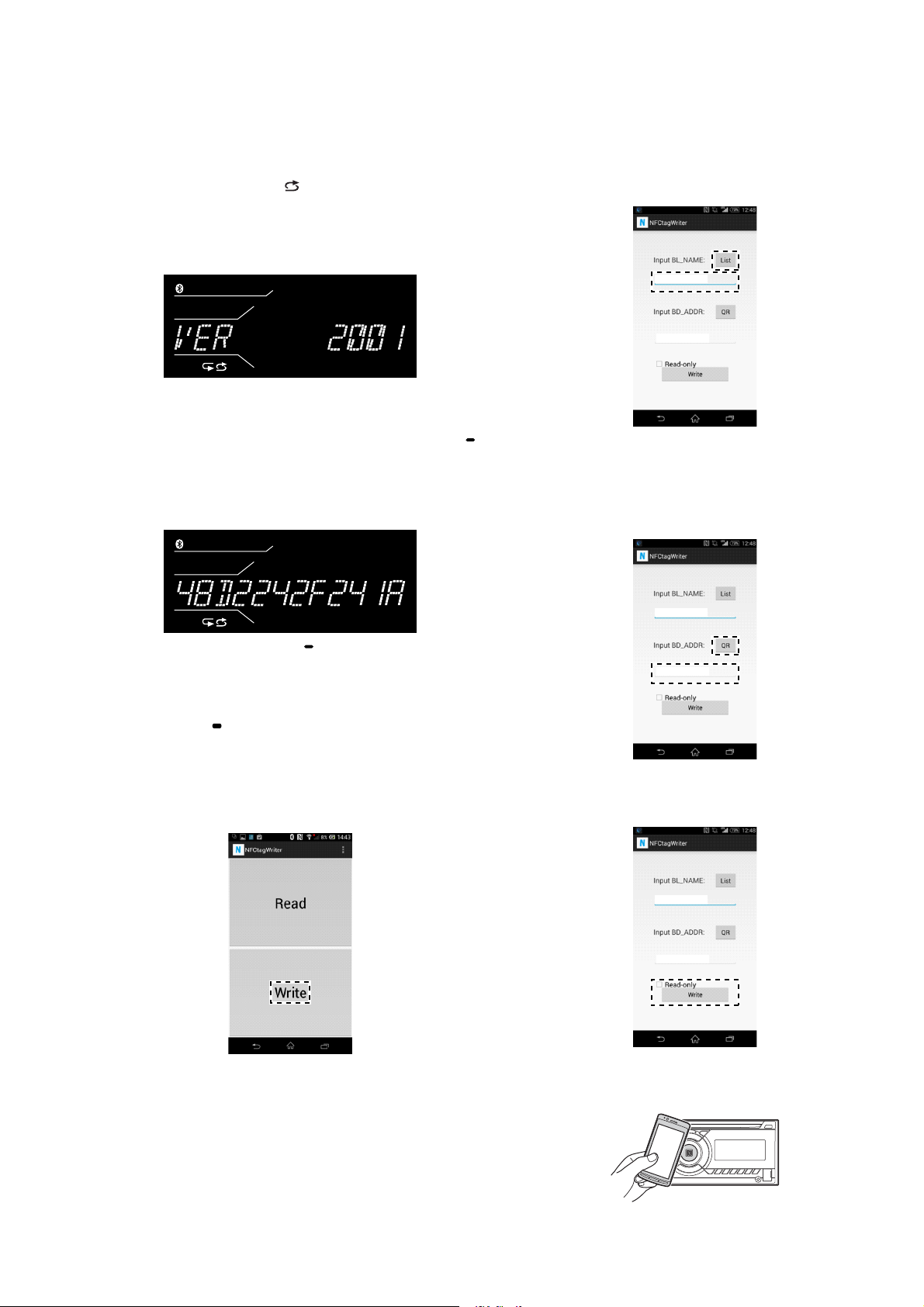
5. Input the Bluetooth Local Name (BL_NAME).
Tap the “List” on the screen of the smartphone and select the
model name of the this unit. If there is not model name of the
this unit on the list, please input the model name with the keyboard on the smartphone.
Bluetooth Local Name
Bluetooth Device Addres
6. Input the Bluetooth address (BD_ADDR).
Input the Bluetooth address (BD_ADDR) that was checked by
step 1 with the keyboard on the smartphone, or tap the “QR”
on the screen of the smartphone and read the barcode with the
camera of the smartphone.
Note 1: When pressing the [DSPL SCRL] button again, the destina-
tion code is displayed on the liquid crystal display, but it is
not necessary to display in this step.
3 The resetting operation is executed by pressing the
[SOURCE
OFF] button for 1 second after the confi rming
ends, and the unit returns to the normal condition.
2. Turn on the NFC function of the smartphone.
3. Start the NFC Tag Data Writing Application on the smartphone.
4. Tap the “Write” on the screen of the smartphone.
WX-900BT
Bluetooth Device Addres
7. Tap the “Write” on the screen of the smartphone, in the state
that unchecked the box “Read-only”.
WX-900BT
48D2242F241A
8. Touch the N-mark part of the smartphone to the N-mark part of
the unit.
– Continued on next page –
11
Page 12
WX-850BT/900BT/900BTM
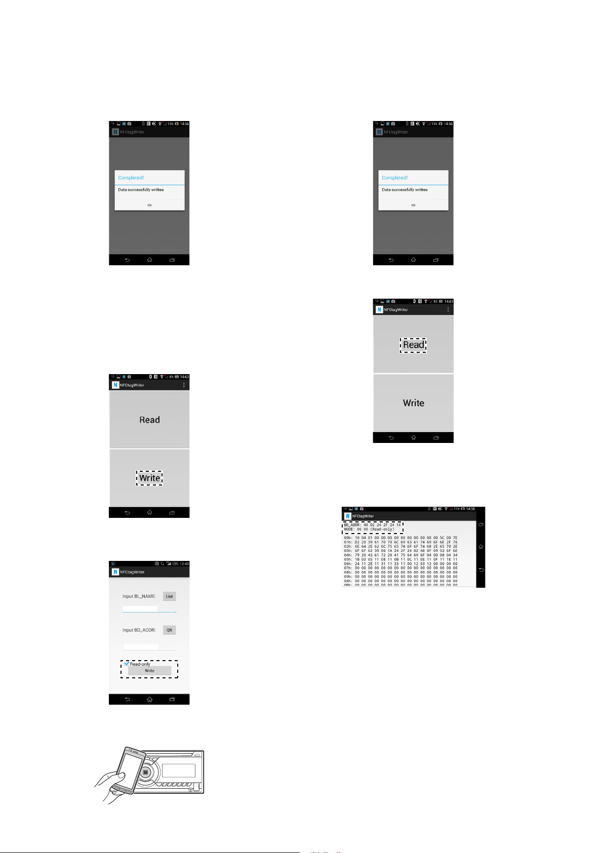
9. Check that “Completed!” is displayed on the screen of the
smartphone.
Note 2: When “Completed!” is not displayed on the screen of the smart-
phone, refer to “3. Error Display” on page 13.
10. End the NFC Tag Data Writing Application on the smartphone.
11. Check the operation of connecting with the smartphone by one
touch (NFC).
(Refer to “OPERATION CHECK OF THE NFC AFTER
COMPLETING THE REPAIRS” on page 15)
12. Start the NFC Tag Data Writing Application on the smartphone.
13. Tap the “Write” on the screen of the smartphone.
16. Check that “Completed!” is displayed on the screen of the
smartphone.
Note 3: When “Completed!” is not displayed on the screen of the smart-
phone, refer to “3. Error Display” on page 13.
17. Tap the “Read” on the screen of the smartphone.
14. Check the box “Read-only” on the screen of the smartphone,
and tap the “Write” on the screen of the smartphone.
WX-900BT
48D2242F241A
15. Touch the N-mark part of the smartphone to the N-mark part of
the unit.
18. Check that “BD_ADDR” on the screen of the smartphone accords with BD_ADDR written on the BT module label and
“MODE” on the screen of the smartphone is “00 00 (Readonly)”.
19. End the NFC Tag Data Writing Application on the smartphone.
20. Check the operation of connecting with the smartphone by one
touch (NFC).
(Refer to “OPERATION CHECK OF THE NFC AFTER
COMPLETING THE REPAIRS” on page 15)
12
Page 13
WX-850BT/900BT/900BTM
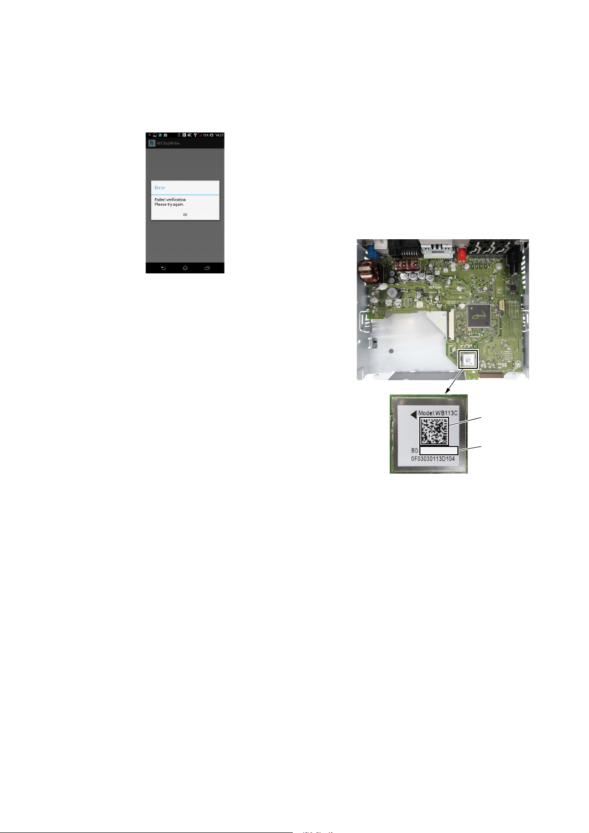
3. Error Display
When the writing of the NFC tag data has failed, “Error” is displayed on the screen of the smartphone.
When “Error” is displayed on the screen of the smartphone, operate according to the procedure below.
Procedure:
1. Tap the “Write” on the screen of the smartphone to write of the
NFC tag data again.
2. When “Error” is displayed on the screen of the smartphone
again, tap the “Read” on the screen of the smartphone.
3. Check that “MODE” on the screen of the smartphone is not
“00 00 (Read-only)”.
4. When “MODE” on the screen of the smartphone is “00 00
(Read-only)”, execute the writing of the NFC tag data again
after replacing the knob (VOL) assy (Ref. No. NFC1).
(When “MODE” on the screen of the smartphone is “00 00
(Read-only)”, the writing of the NFC tag data cannot execute)
4. Check Method of the NFC Tag Data
Check the NFC tag data according to the procedure below.
Procedure:
1. Check the Bluetooth address (BD_ADDR).
There are following two checking methods.
• How to read from the BT module label
• How to display on the liquid crystal display by the test
mode
How to read from the BT module label:
Set the unit to the state where the BT module on the MAIN
board can be seen.
(Refer to “3. DISASSEMBLY” on
page 22 and after)
– MAIN Board (Component Side) –
BD_ADDR
(Barcode)
48D2242F241A
BT module label
BD_ADDR
– Continued on next page –
13
Page 14
WX-850BT/900BT/900BTM
How to display on the liquid crystal display by the
test mode:
1 In the state of source off (the clock is displayed on the
liquid crystal display), enter the test mode by pressing the
buttons in order of the [
(press only the [PAUSE 6] button for two seconds).
(Displayed characters/values in the following fi gure are
example)
Software main version
2 In the state in which the software main version is displayed
on the liquid crystal display, enter the Bluetooth address
(BD_ADDR) display mode by pressing the [DSPL
SCRL] button.
(Displayed characters/values in the following fi gure are
example)
Bluetooth address (BD_ADDR)
4] t [MIC 5] t [PAUSE 6]
5. Check that “BD_ADDR” on the screen of the smartphone accords with BD_ADDR written on the BT module label and
“MODE” on the screen of the smartphone is “00 00 (Readonly)”.
6. End the NFC Tag Data Writing Application on the smartphone.
Note: When pressing the [DSPL SCRL] button again, the destina-
3 The resetting operation is executed by pressing the
2. Turn on the NFC function of the smartphone.
3. Start the NFC Tag Data Writing Application on the smart-
4. Tap the “Read” on the screen of the smartphone.
tion code is displayed on the liquid crystal display, but it is not
necessary to display in this step.
[SOURCE
ends, and the unit returns to the normal condition.
phone.
OFF] button for 1 second after the confi rming
14
Page 15
5. The Factor that One Touch Connection is Impossible
The four following factors are considered as the factor that one touch connection is impossible.
Guess and check the defective factor by each checking result.
Note: The four following factors are examples.
WX-850BT/900BT/900BTM
Factor
1 BT module defect NG ― NG NG
knob (VOL) assy
2
defect
NFC tag data
3
writing failure
4 Smartphone OK OK OK NG
IMPORTANT NOTE OF INITIALIZING
The purpose of “Bluetooth Initialize” is to initialize the Bluetooth
connection history (HF/Audio Streaming). (To delete the device
information for the devices that you connected to when searching,
etc.)
Bluetooth manual con-
nection check by user
OK NG OK NG
OK NG OK NG
NFC tag data check
OPERATION CHECK OF THE NFC AFTER COMPLETING THE REPAIRS
After completing the repairs of this unit, follow the procedure below
to check normal operation of the NFC.
Note: After checking of NFC operation, be sure to delete the pairing infor-
When the complete MAIN board is replaced, it is necessary to ini-
Bluetooth manual connec-
tion check by servicing
mation before returning this unit to the customer.
NFC one touch connection
check with smartphone
tialize this unit.
Refer to the following, initialize this unit.
Note: Phonebook data and dialed/received call history can be deleted by
executing “Bluetooth Initialize”.
Procedure:
1. In the state of source off (the clock is displayed on the liq-
uid crystal display), press the [v PUSH ENTER/MENU/
VOICE] button.
2. Rotate the control dial, and select the “SET BT”.
3. Press the [v PUSH ENTER/MENU/ VOICE] button.
4. Rotate the control dial, and select the “SET BT INIT”.
5. Press the [v PUSH ENTER/MENU/ VOICE] button, and the
message “SET INIT-NO” is displayed on the liquid crystal display.
6. Rotate the control dial clockwise, and the message “SET INITYES” is displayed on the liquid crystal display.
7. Press the [v PUSH ENTER/MENU/ VOICE] button.
8. When “Bluetooth Initialize” is completed, the message
“COMPLETE” is displayed on the liquid crystal display for a
moment.
9. Press the [MODE ] button twice, and return to the state of
Connecting with a Smartphone by One
touch (NFC)
By touching the control dial on the unit with an
NFC* compatible smartphone, the unit is paired and
connected with the smartphone automatically.
* NFC (Near Field Communication) is a technology
enabling short-range wireless communication
between various devices, such as mobile phones and
IC tags. Thanks to the NFC function, data
communication can be achieved easily just by
touching the relevant symbol or designated location
on NFC compatible devices.
For a smartphone with Android OS 4.0 or lower
installed, downloading the app “NFC Easy Connect”
available at Google Play™ is required. The app may
not be downloadable in some countries/regions.
1 Activate the NFC function on the
smartphone.
For details, refer to the operating instructions
supplied with the smartphone.
2 Touch the N-Mark part of the unit with
the N-Mark part of the smartphone.
source off (the clock is displayed on the liquid crystal display).
Make sure that lights up on the display of the
unit.
To disconnect by One touch
Touch the N-Mark part of the unit with the N-Mark
part of the smartphone again.
Notes
ˎ When making the connection, handle the
smartphone carefully to prevent scratches.
ˎ One touch connection is not possible when the unit is
already connected to another NFC compatible device.
In this case, disconnect the other device, and make
connection with the smartphone again.
15
Page 16
WX-850BT/900BT/900BTM
)
Ver. 1.1
(US and Canadian models)
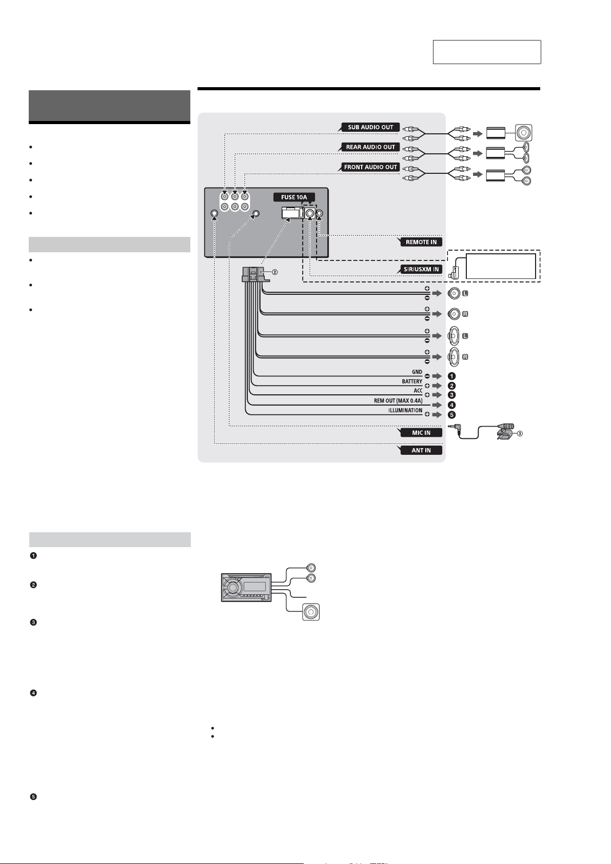
Connection/Installation
Cautions
Run all ground (earth) leads to a common
ground (earth) point.
Do not get the leads trapped under a screw, or
caught in moving parts (e.g., seat railing).
Before making connections, turn the car ignition
o to avoid short circuits.
Connect the yellow and re d power supply leads
only after all other leads have been connected.
Be sure to insulate any loose unconnected leads
with electrical tape for safety.
Precautions
Choose the installation location carefully so that
the unit will not interfere with normal driving
operations.
Avoid installing the unit in areas subject to dust,
dirt, excessive vibration, or high temperature,
such as in direct sunlight or near heater ducts.
Use only the supplied mounting hardware for a
safe and secure installation.
Note on the power supply lead (yellow)
When connecting this unit in comb ination with other
stereo components, the amperage rating of the car
circuit to which the unit is connected must be highe r
than the sum of each component’s fuse amperage
rating.
Mounting angle adjustment
Adjust the mounting angle to less than 45°.
Connection
SECTION 2
GENERAL
White
White/black striped
Gray
Gray/black striped
Green
Green/black striped
Purple
Purple/black striped
Black
Yel l ow
Red
Blue/white striped
Orange/white striped
This section is extracted
from operating instruction.
3
*
3
*
3
*
Power ampli er*
from a wire d remote cont rol
(not supplied)*
4
Satellite radio tuner
1
(SiriusXM)*
1*2
Front speaker*
Rear speaker*1*
For details, see “Making
connections”.
2
Subwoofer*
1
(900BT only
1
Making connections
To a common ground (earth) point
First connect the black ground (earth) lead, then
connect the yellow and red power supply leads.
To the +12 V power terminal which is
energized at all times
Be sure to rst connect the black ground (earth)
lead to a common ground (earth) point.
To the +12 V power terminal which is
energized when the ignition switch i s set to
the accessor y position
If there is no accessory position, connect to the
+12 V power (battery) terminal which is
energized at all times.
Be sure to rst connect the black ground (earth)
lead to a common ground (earth) point.
To the power antenna (aerial) control lead or
the power supply lead of the antenna (aerial)
booster
It is not necessa ry to connect this le ad if there is
no power antenna (aerial) or antenna (aerial)
booster, or with a manually-operated telescopic
antenna (aerial).
To AMP REMOTE IN of an optional power
amplier
This connection is only for ampliers and a
power antenna (aerial). Connecting any other
system may damage the unit.
To a car’s illumination signal
Be sure to rst connect the black ground (earth)
lead to a common ground (earth) point.
*1 Not supplied
*2 S peaker impedance: 4 – 8 Ω × 4
*3 RC A pin cord (not supplied)
*4 De pending on the type of car, use an adaptor for a
wired rem ote control (not su pplied).
Subwoofer Easy Connection
You can use a subwoofer without a power amplier
when it is connected to a rear speaker cord.
Front speaker
Subwoofer
Note
Use a subwoofer with an impedance of 4 to 8 ohms,
and with adequate power handling capacities to avoid
damage.
Memory hold connection
When the yellow power supply lead is connected,
power will always be supp lied to the memory
circuit even when the ignition switch is turned o.
Speaker connection
Before connecting the speakers, turn the unit o.
Use speakers with an impedance of 4 to 8 ohms,
and with adequate power handling capacities to
avoid damage.
6
*5*
from a car antenna (aerial)
*5 Whethe r in use or not, route the microphone input
cord such that it does not interfere with driving
operations. Secure the cord with a clamp, etc., if it is
installed around your feet.
*6 For details on installing the microphone, see
“Installing the microphone”.
16
Page 17
WX-850BT/900BT/900BTM
T
Ver. 1.1
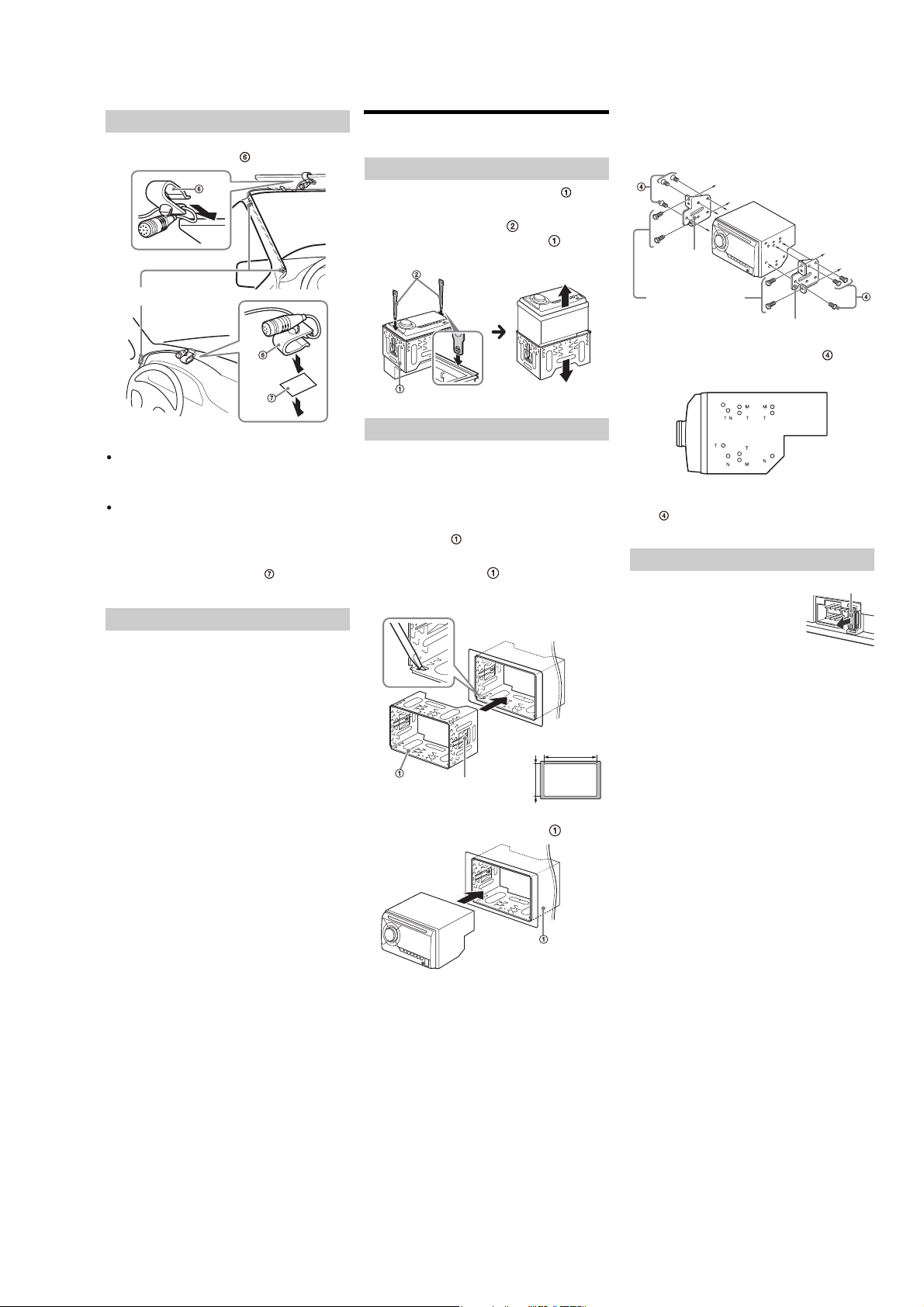
Installing the microphone
o capture your voice during handsfree calling, you
need to install the microphone .
Notes on ins talling the con nection cable RC-SR1 (not
supplied)
Refer to the support sites on the back cover for
details, then connect each lead properly to the
appropriate leads. Making an improper connection
may damage the unit.
Depending on the type of car, be sure to insulate the
unused leads with electrical tape for safety.
Do not connect this cable when the steering wheel
remote control is not used.
Consulting the dealer or an experienced technician
for help is recommended .
When using the wired remote control
1 To enable the wired remote control, set [STR
Clip (not supplied)
CONTROL] in [SET STEERING] to [PRESET].
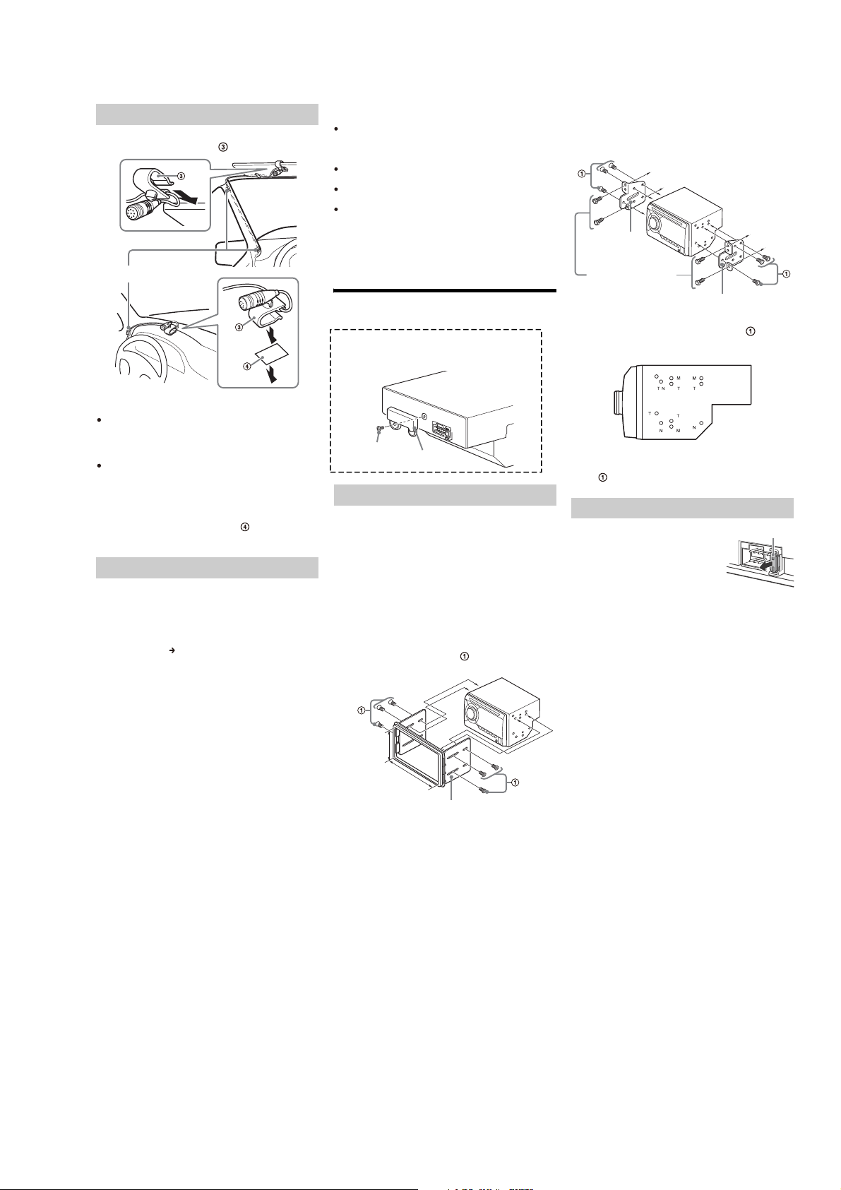
Installation
(850BT only)
Before installing this unit, remove the screw and
box on the back of the unit. Do not use the previous
parts you removed when installing the unit.
Cautions
It is extremely dangerous if the cord becomes
wound around the steering column or gearstick.
Be sure to keep it and other parts from interfering
with your driving operations.
If airbags or any other shock-absorbing
equipment is in your car, contact the store where
you purchased this unit, or the car dealer, before
installation.
Note
Before attaching the double-sided tape , clean the
surface of the dashboard with a dry cloth.
Using the wired remote control
When using the steering wheel remote
control
Installation of the connection cable RC-SR1 (not
supplied) is required before use.
1 To enable the steering wheel remote control, select
[SET STEERING] [EDIT CUSTOM] to make the
regist ration.
When the regis tration completes, the st eering wheel
remote control becomes available.
Screw
Box
Mounting the unit in the dashboard
When mounting in a Japanese car, see “Mounting
the unit in a Japanese car”.
Mounting the unit with an installation kit
(not supplied)
You can use a commercially available double DIN
installation kit. Choose a n installation kit with the
following panel frame size.
Larger than 172 × 97 mm (6
an inner corner radius of less than 0.5 mm (
Note
Be sure to use the supplied screws .
7
/ 8 × 3 7/ 8 in) (w/h), with
to dashboard/center console
1
/ 32 in).
Mounting the unit in a Japanese car
You may not be able to install this unit in some
makes of Japanese cars. In such a case, consult your
Sony dealer.
to dashboard/center console
Bracket
Existing parts sup plied
with your car
Bracket
When mounting this unit to the preinstalled
brackets of your car, use the supplied screws in
the appropriate screw holes, based on your car: T
for TOYOTA, M for MITSUBISHI and N for NISSAN.
Note
To prevent malfunction, install only with the supplied
screws .
Fuse replacement
When replacing the fuse, be sure
to use one matching the
amperage rating stated on the
original fuse. If the fuse blows,
check the power connection and
replace the fuse. If the fuse blows
again after replacement, there
may be an internal malfunction. In such a case,
consult your nearest Sony dealer.
Fuse (10 A)
Larger than
97 mm (3
7
/8 in)
Larger than
172 mm (6 7/ 8 in)
Installation kit (not suppl ied)
17
Page 18
WX-850BT/900BT/900BTM
(AEP and UK models)
Connection/Ins tallation
Cautions
Run all ground (earth) leads to a common
ground (earth) point.
Do not get the leads trapped under a screw, or
caught in moving parts (e.g., seat railing).
Before making connections, turn the car ignition
o to avoid short circuits.
Connect the power supply lead to the unit and
speakers before connecting it to the auxiliary
power connector.
Be sure to insulate any loose unconnected leads
with electrical tape for safety.
Precautions
Choose the installation location carefully so that
the unit will not interfere with normal driving
operations.
Avoid installing the unit in areas subject to dust,
dirt, excessive vibration, or high temperature,
such as in direct sunlight or near heater ducts.
Use only the supplied mounting hardware for a
safe and secure installation.
Note on the power supply lead (yellow)
When connecting this unit in comb ination with other
stereo components, the amperage rating of the car
circuit to which the unit is connected must be highe r
than the sum of each component’s fuse amperage
rating.
Mounting angle adjustment
Adjust the mounting angle to less than 45°.
Connection
See “Power connection diagram”
for details.
*1 Not supplied
*2 S peaker impedance: 4 – 8 Ω × 4
*3 R CA pin cord (not supplied)
*4 De pending on the type of car, use an adaptor for a
wired rem ote control (not su pplied).
*5 Depending o n the type of car, use an adaptor (not
supplied) if the antenna (aerial) connector does not
t.
3
*
3
*
3
*
from a wire d remote contro l
(not supplied)*
2
*
from a car antenna (aerial)*
*6 Whether in use or not, route the microphone input
cord such that it does not interfere with driving
operations. Secu re the cord with a cla mp, etc., if it is
installed around your feet.
*7 For details on installing the microphone, see
“Installing the microphone”.
Power amplier*
4
For details, see “Maki ng
connections”.
Subwoofer*
1
5
1
7
*6 *
Making connections
If you have a power antenna (aerial ) without a relay
box, connecting this unit with the supplied power
supply lead may damage the antenna (aerial).
To the car’s speaker connector
1
Rear speake r
(right)
2
3
Front speaker
(right)
4
5
Front speaker
(left)
6
7
Rear speake r
(left)
8
To the car’s power connector
continuous power
12
supply
power antenna (aerial) /
13
power amplier control
(REM OUT)
switched illumination
14
power supply
16 ground (earth) Black
Purple
Purple/black
striped
Gray
Gray/black str iped
White
White/black
striped
Green
Green/bla ck
striped
Yel l o w
Blue/white striped
Orange/white
striped
Redswitched power suppl15
Subwoofer Easy Connection
You can use a subwoofer without a power amplier
when it is connected to a rear speaker cord.
Front speaker
Subwoofer
Notes
Preparation of the rear speaker cords is required.
Use a subwoofer with an impedance of 4 to 8 ohms,
and with adequate power handling capacities to
avoid damage.
Memory hold connection
When the yellow power supply lead is connected,
power will always be supplied to the memory
circuit even when the ignition switch is turned o.
Speaker connection
Before connecting the speakers, turn the unit o.
Use speakers with an impedance of 4 to 8 ohms,
and with adequate power handling capacities to
avoid damage.
Power connection diagram
Make sure your car’s auxiliary power conn ector, and
match the connecti ons of cords correctly
depending on the car.
Auxiliary power connector
Common connection
Red Red
Yellow Yellow
continuous power
12
supply
Yel lo w
Redswitched power supply15
When the positions of the red and yellow
leads are inverted
Red Red
Yellow Yellow
Yellowswitched power supply 12
continuous power
15
supply
Red
When the car without ACC position
Red
Yel l o w
After matching the connections and switching
power supply leads correctly, connect the unit to
the car’s power supply. If you have any questions
and problems connecting your unit that are not
covered in this manual, consult the car dealer.
Red
Yel l o w
18
Page 19
WX-850BT/900BT/900BTM
Installing the microphone
To capture your voice during handsfree calling, you
need to install the microphone .
Clip (not supplied)
Cautions
It is extremely dangerous if the cord becomes
wound around the steering column or gearstick.
Be sure to keep it an d other parts from interfe ring
with your driving operations.
If airbags or any other shock-absorbing
equipment is in your car, contact the store where
you purchased t his unit, or the car dealer, before
installation .
Note
Before attaching the double-sided tape , clean the
surface of the dashboard with a dry cloth.
Using the wired remote control
1 To enable the wired remote control, set
[STR CONTROL] in [SET STEERING] to
[PRESET].
Installation
Removing the bracket
Before installing the unit, remove the bracket
from the unit.
1 Insert both release keys until they
click, and pull down the bracket , then
pull up the unit to separate.
Face the hook inwards.
Mounting the unit in the dashboard
When mounting in a Japanese car, see “Mounting
the unit in a Japanese car”.
Mounting the unit with the supplied
bracket
Before installing, make sure the catches on both
sides of the bracket are bent inwards 3.5 mm
5
(
/ 32 in).
1 Position the bracket inside the
dashboard, then bend the claws outward
for a tight t.
Mounting the unit in a Japanese car
You may not be able to install this unit in some
makes of Japanese cars. In such a case, consult your
Sony dealer.
to dashboard/center console
Bracket
Existing parts supplied
with your car
Bracket
When mounting this unit to the preinstalled
brackets of your car, use the supplied screws in
the appropriate screw holes, based on your car: T
for TOYOTA, M for MITSUBISHI and N for NISSAN.
Note
To prevent malfunction, install only with the supplied
screws .
Fuse replacement
When replacing the fuse, be sure
to use one matching the
amperage rating stated on the
original fuse. If the fuse blows,
check the power connection and
replace the fuse. If the fuse blows
again after replacement, there
may be an internal malfunction. In such a case,
consult your nearest Sony dealer.
Fuse (10 A)
Larger than
182 mm (7
Larger than
111 mm
Catch
3
/ 8 in)
(4
2 Mount the unit onto the bracket .
Note
If the catches are straight or bent outwards, the uni t will
not be installed securely and may spri ng out.
1
/4 in)
19
Page 20

WX-850BT/900BT/900BTM
(E, Indian and Australian models)
Connection/Installation
Cautions
Run all ground (earth) leads to a common
ground (earth) point.
Do not get the leads trapped under a screw, or
caught in moving parts (e.g., seat railing).
Before making connections, turn the car ignition
o to avoid short circuits.
Connect the yellow and red power supply leads
only after all other leads have been connected.
Be sure to insulate any loose unconnected leads
with electrical tape for safety.
Precautions
Choose the installation location carefully so that
the unit will not interfere with normal driving
operations.
Avoid installing the unit in areas subjec t to dust,
dirt, excessive vibration, or high temperature,
such as in direct sunlight or near heater ducts.
Use only the supplied mounting hardware for a
safe and secure installation.
Note on the power supply lead (yellow)
When connecting this u nit in combination with other
stereo components, the amperage rating of the car
circuit to which the unit is connected must be high er
than the sum of each component’s fuse amperage
rati ng.
Mounting angle adjustment
Adjust the mounting angle to less than 45°.
Connection
White
White/black striped
Gray
Gray/black striped
Green
Green/black striped
Purple
Purple/black striped
Black
Yel l o w
Red
Blue/white striped
Orange/white striped
3
*
3
*
3
*
from a wired remote control
(not supplied)*
Power ampli er*
4
Front speaker*1*
Rear speaker*1*
For details, see “Maki ng
connections”.
Subwoofer*
1
2
2
1
Making connections
To a common ground (earth) point
First connect the black ground (earth) lead, then
connect the yellow and red power supply leads.
To the +12 V power terminal which is
energized at all times
Be sure to rs t connect the black ground (earth)
lead to a common ground (earth) point.
To the +12 V power terminal which is
energized when the ignition switch is set to
the accessory pos ition
If there is no accessory position, connect to the
+12 V power (battery) terminal which is
energized at all times.
Be sure to rs t connect the black ground (earth)
lead to a common ground (earth) point.
*1 Not supplied
*2 Spe aker impedance: 4 – 8 Ω × 4
*3 RCA pi n cord (not supplied)
*4 Depending on the type of car, use an adaptor for a
wired remote control (not supplied).
To the power antenna (aerial) control lead or
the power supply lead of the antenna (aerial)
booster
It is not necessar y to connect this lead i f there is
no power antenna (aerial) or antenna (aerial)
booster, or with a manually-operated telescopic
antenna (aerial).
To AMP REMOTE IN of an optional power
mplier
a
This connection is only for ampliers and a
power antenna (aerial). Connecting any other
system may damage the unit.
To a car’s illumination signal
Be sure to rs t connect the black ground (earth)
lead to a common ground (earth) point.
from a car antenna (aeria l)
*5 Whethe r in use or not, route the microphone input
cord such that it does not interfere with driving
operations. Secure the cord with a clamp, etc., if it is
installed around your feet.
*6 For details on installing the microphone, see
“Installing the microphone”.
Subwoofer Easy Connection
You can use a subwoofer without a power amplier
when it is connected to a rear speaker cord.
Front speaker
Subwoofer
Note
Use a subwoofer with an impedance of 4 to 8 ohms,
and with adequate power handling capaciti es to avoid
damage.
Memory hold connection
When the yellow power sup ply lead is connected,
power will always be supplied to the memory
circuit even when the ignition switch is turned o.
Speaker connection
Before connecting the speakers, turn the unit o.
Use speakers with an impedance of 4 to 8 ohms,
and with adequate power handling capacities to
avoid damage.
6
*5*
20
Page 21

WX-850BT/900BT/900BTM
Installing the microphone
To capture your voice during handsfree calling, you
need to install the microphone .
Clip (not supplied)
Cautions
It is extremely dangerous if the cord becomes
wound around the steering column or gearstick.
Be sure to keep it and ot her parts f rom interfer ing
with your driving operations.
If airbags or any other shock-absorbing
equipment is in your car, contact the store where
you purchased this unit, or the car dealer, before
installation.
Note
Before attaching the double-sided tape , clean the
surface of the dashboard with a dry cloth.
Using the wired remote control
1 To enable the wired remote control, set
[STR CONTROL] in [SET STEERING] to
[PRESET].
Installation
Mounting the unit in the dashboard
When mounting in a Japanese car, see “Mounting
the unit in a Japanese car”.
Mounting the unit with an installation kit
(not supplied)
You can use a commercially available double DIN
installation kit. Choose an installation kit with the
following panel frame size.
Larger than 172 × 97 mm (6
an inner corner radius of less than 0.5 mm (
Note
Be sure to use the supplied screws .
Larger than
7
97 mm (3
/8 in)
Larger than
172 mm (6 7/8 in)
7
/ 8 × 3 7/ 8 in) (w/h), with
to dashboard/center console
Installation kit (not suppl ied)
1
/ 32 in).
Mounting the unit in a Japanese car
You may not be able to install this unit in some
makes of Japanese cars. In su ch a case, consult your
Sony dealer.
to dashboard/center console
Bracket
Existing parts sup plied
with your car
Bracket
When mounting this unit to the preinstalled
brackets of your car, use the supplied screws in
the appropriate screw holes, based on your car: T
for TOYOTA, M for MITSUBISHI and N for N ISSAN.
Note
To prevent malfunction, install only with the supplied
screws .
Fuse replacement
When replacing the fuse, be sure
to use one matching the
amperage rating stated on the
original fuse. If the fuse blows,
check the power connection and
replace the fuse. If the fuse blows
again after replacement, there
may be an internal malfunction. In such a case,
consult your nearest Sony dealer.
Fuse (10 A)
21
Page 22

WX-850BT/900BT/900BTM
DISASSEMBLY
• This set can be disassembled in the order shown below.
3-1. DISASSEMBLY FLOW
SET
SECTION 3
3-2. MINI FUSE (BLADE TYPE) (FU1),
COVER
(Page 22)
3-3. PANEL FRONT BLOCK
(Page 23)
3-4. CD MECHANISM DECK (MG-101CF-188)
(Page 24)
3-5. MAIN BOARD
(Page 25)
Note: Follow the disassembly procedure in the numerical order given.
3-2. MINI FUSE (BLADE TYPE) (FU1), COVER
5 cover
3-7. SERVICE POSITION
(Page 27)
3-6. KNOB (VOL) ASSY (NFC1),
PANEL FRONT ASSY,
KEY BOARD
(Page 26)
When installing the cover,
Note:
that four bosses are all locked.
OK
check
3 two bosses
4 three claws
3 two bosses
1 mini fuse (blade type)
(FU1)
Boss is locked.
NG
Boss is unlocked.
Insert the screwdriver into
2
the slit, and lift up the cover.
22
Page 23

3-3. PANEL FRONT BLOCK
2
Remove the panel front block
in the direction of the arrow.
4 panel front block
1 two claws
3
connector
(
CN101
WX-850BT/900BT/900BTM
)
main block
1 two claws
1 two claws
When installing the cable flexible flat (22 core) to the connector (CN101)
Note:
on the MAIN board, insert straight to the connector and lock a connector
completely. No slanting after insertion.
NG
Insert is incline.Insert is straight to the interior.
connector
cable flexible flat
(22 core)
OK
connector
cable flexible flat
(22 core)
23
Page 24

WX-850BT/900BT/900BTM
3-4. CD MECHANISM DECK (MG-101CF-188)
Note 1: The service manual of the mechanism deck, used in this mod-
el has been issued in a separate volume. Please refer to the
service manual of the MG-101 series for the mechanism deck
information.
When installing the CD mechanism
Note 2:
block, align the rib and the slot.
4
Unlock the connector.
(
CN401
)
8 CD mechanism deck
(MG-101CF-188)
7 bracket (CD)
6 two
screws
(PTT2.6
Note 2:
block, align the rib and the slot.
u
4)
When installing the CD mechanism
5 cable flexible flat
(27 core)
+RZWRLQVWDOOWKH&'PHFKDQLVPGHFN
CN401
(FFC1)
1
two screws
(PTT2.6
2 Lock the connector.
u
6)
3
Unlock the connector.
(
CN701
1
screw
(PTT2.6
)
u
6)
slot
3 cable flexible flat
(27 core)
2
Lift up the
in the direction of the arrow.
rear side
slot
1
(PTT2.6
main block
(FFC1)
4 Lock the connector.
CD mechanism block
screw
u
6)
5
terminal side
1 cable flexible flat
(27 core)
Note 3:
and lock a connector completely. No slanting after insertion.
Insert is straight to the interior.
cable flexible flat
(27 core)
(FFC1)
When installing the cable flexible flat (27 core) (FFC1),
OK
(FFC1)
connector
CN701
Connector is unlock.
cable flexible flat
(27 core)
connector
24
NG
(FFC1)
insert straight to the connector
NG
Insert is incline.
cable flexible flat
(27 core)
(FFC1)
connector
NG
Insert is shallow.
cable flexible flat
(27 core)
(FFC1)
connector
Page 25

3-5. MAIN BOARD
Note 1: When the complete MAIN board is replaced, it is necessary
to replace knob (VOL) assy (Ref. No. NFC1) simultaneously.
Also, the destination setting, Bluetooth operation check and
Bluetooth information writing is necessary. Refer to “DESTINATION SETTING METHOD” on page 5, “BLUETOOTH
FUNCTION CHECKING METHOD USING A SMARTPHONE OR CELLULAR PHONE” on page 8 and “BLUETOOTH INFORMATION WRITING METHOD” on page 9.
4 MAIN board
Note 2:
align the hole and claw.
The sheet heat transfer must be pasted
Note 3:
on this position.
However, when the MAIN board is
removed, the sheet heat transfer may
adhere to the MAIN board.
Paste the sheet heat transfer on this
place again then.
When installing the MAIN board,
1
screw
(PTT2.6
u
WX-850BT/900BT/900BTM
8)
2 two ground point screws
(PTT2.6 u 6)
1
screw
(PTT2.6
u
8)
sheet heat transfer
guide line
front side
+RZWRLQVWDOOWKH0$,1ERDUG
MAIN board
hole
front side
claw
chassis block
hole
3 claw
rear side
chassis block
25
Page 26

WX-850BT/900BT/900BTM
3-6. KNOB (VOL) ASSY (NFC1), PANEL FRONT ASSY, KEY BOARD
Note 1: When the knob (VOL) assy (Ref. No. NFC1) is replaced,
Bluetooth information writing is necessary. Refer to “BLUETOOTH INFORMATION WRITING METHOD” on page 9.
When installing the cable flexible flat (22 core) (FFC2) to the connector (CN901) on the KEY board,
Note 2:
insert straight to the connector and lock a connector completely. No slanting after insertion.
OK
Insert is straight to the interior.
connector
connector
NG
Connector is unlock. Insert is incline.
NG
connector
cable flexible flat
(22 core)
%7$(38K($86
,QVWDOODWLRQSRVLWRQRIWKHJDVNHW
VKLHOGWXQH6
gasket
(shield tune S)
5
7
(22 core) (FFC2)
(FFC2)
KEY board
guide line
gasket (shield tune S)
6
Unlock the connector.
(
cable flexible flat
The lower side is
the terminal side.
guide line
–5HDUYLHZ–
CN901
)
cable flexible flat
(22 core)
2
screw
(B P-TITE M2)
8
filament tape
(sub material)
(FFC2)
9 KEY board
cable flexible flat
(22 core)
(FFC2)
front side
1 knob (VOL) assy
(NFC1)
4 panel front assy
3 Remove the KEY board block
in the direction of the arrow.
3DVWLQJSRVLWLRQRIWKHILODPHQWWDSHVXEPDWHULDO
Paste the filament tape (sub material) to prevent the cable
Note 3:
flexible flat (22 core) (FFC2) is damaged in touch with
the sheet metal.
Cover the sheet metal.
guide line
–5HDUYLHZ–
26
KEY board
CN901
filament tape
(sub material)
2
five screws
(B P-TITE M2)
Page 27

SECTION 4
TEST MODE
WX-850BT/900BT/900BTM
3-7. SERVICE POSITION
Note 1: The service position below cannot be performed with the fl ex-
ible fl at cable (length: 80 mm) used with the unit. Refer to
“NOTE OF PERFORMING THE OPERATION CHECK” in
the servicing notes, and use a long fl exible fl at cable (length:
150 mm).
insulating sheet
stand
cable flexible flat (27 core)
(length: 150 mm)
Do not cable flexible flat (27 core) is
Note 2:
damaged by the edge of the chassis.
CD mechanism deck CD mechanism deck
main unit
main unit
OKOK
insulating sheet
stand
cable flexible flat (27 core)
(length: 150 mm)
Do not cable flexible flat (27 core) is
Note 2:
damaged by the edge of the chassis.
SETTING THE TEST MODE
Setting method:
1. In the state of source off (the clock is displayed on the liquid
crystal display), enter the test mode by pressing the buttons in
order of the [
the [
ALBUM 1] button for two seconds).
V
4] t [MIC 5] t [
ALBUM 1] (press only
V
2. It is set to the test mode, and all segments of the liquid crystal
display light.
Releasing method:
Press the [SOURCE OFF] button for 1 second.
MICROPHONE AUDIO LOOPBACK
To confi rm the state of the external microphone used when a
handsfree function is used, the microphone audio is output from
the speaker.
The breakdown judgment of the microphone can be done without
connecting H/F with the smartphone or cellular phone.
Procedure:
1. Enter the test mode.
2. Press the [SOURCE OFF] button to select the “BT PHONE”
function.
3. On/off of the microphone audio loopback function changes
whenever the [ALBUM
2] button is pressed (“ ” (album
v
mark) is displayed on the liquid crystal display).
Screen display
cable flexible flat (27 core)
(length: 150 mm)
NG
CD mechanism deck
CD mechanical deck should
Note 3:
not be placed vertically.
main unit
NG
CD mechanism deck
CD mechanical deck should
Note 4:
not be placed upside down.
CD mechanism deck
CD mechanical deck should
Note 3:
not be placed vertically.
main unit
NG
cable flexible flat (27 core)
(length: 150 mm)
AF
album mark
LOOPBACK
ON Lit
OFF None
(album mark)
cable flexible flat (27 core)
(length: 150 mm)
WX-850BT/900BT/900BTM
main unit
2727
Page 28

WX-850BT/900BT/900BTM
SECTION 5
DIAGRAMS
5-1. BLOCK DIAGRAM - SERVO/USB/Bluetooth Section -
CD MECHANISM
DECK BLOCK
(MG-101CF-188)
A
C
B 15 FNI2
F 20 TPI
E 21 TNI
1/2VCC
DRV_VREF
PD 24 MDI
AUTOMATIC
LD 25 LDO
FOCUS 31 FOO
TRACK 32 TRO
SL 34 FMO
SP 35 DMO
DRV_ON
LOAD
EJECT
L_SW
D_SW
IN_SW
SELF
ANT001
(BT ANTENNA)
RESET
>001B
POWER CONTROL
Q701
IC1002
BT MODULE
39
PCM2_IN
RF
PCM2_OUT
PCM_CLK
PCM2_SYNC
UART_TX
UART_RX
RESET
25
26
23
24
13
14
12
(Page 30)
CN902
3
D+
2
D–
18 57FPI1 DAO3
17 FPI2
16 FNI1
22 VRO
PIO391PIO492PIO589PIO2
90
27
24
26
47
DRV_ON
60
D501
MEC_LOAD
41
MEC_EJECT
57
MEC_LIMIT
124
MEC_DSW
51
MEC_INSW
137
MEC_SELFSW
54
BT_DOUT
55
BT_DIN
52
BT_CLK
53
BT_SYNC
65
BT_Rx
133
BT_TX
114
BT_RST
151
DP0
150
DM0
BSIF_DO
BSIF_BCK
44
12
BSIF_LR
LRCK_INT
USB_X2
140
28RFRP
RF AMP,
DIGITAL SERVO PROCESSOR,
AUDIO DSP
PIO12
PIO1
PIO15
PIO1943PIO13
42
88
45
49
BUFFER
16
32
33
29
BSIF_GATE
DEC_BCK_IN
BSIF_ST_REQ
DEC_SDOUT_F
DEC_SDIN_CH0
SYSTEM CONTROLLER
USB_X1
139
AUDIO DSP,
IC503 (1/3)
XTAL70EXTAL
71
IC705
IC504
91
PARADISSO_BCK
27 RFZI
PIO1844PIO14
87
48
13
30
DEC_LRCK_IN
68
PIO093PIO6
95
8
6
DEC_INT
DEC_XMUTE
RTC_X2
PIO8/CDMON0
PIO9/CDMON1
BUS280BUS381BUCK82CCE
96
79
5
22
20
CD_SDI
SP_CLK
CD_SDO
SP_DATA
RTC_X1
67
17
19
CD_XCCE
CD_BUSCLK
PIO7
37
94
10
15
CD_ZDET
XO
XI
SRAMSTB
RST
85
14
DSP_RST
DSP_SSTBY
I2C0_SDA
I2C0_SCL
54DAO2
59DAO4
52DAO1 R-CH
61DAO5
70ADIN1
74ADIN2
67
66
R-CH
X701
16.9344MHz
AU_SUB_CH
R-ch is omitted due to same as L-ch.
SIGNAL PATH
SERIAL FLASH
I2C0_SDA
I2C0_SCL
5
2
3
7
6
1
2
6
I2C0_SDA
I2C0_SCL
170SF1_D0
172SF1_D1
166SF1_D2
167SF1_D3
168SF1_CLK
169SF1_CE
126
125
AU_FL_CH
AU_RL_CH
AU_IN_LCH
AU_IN_RCH
IC502
SI/SIO0
SO/SIO1
WP/SIO2
HOLD/SIO3
SCLK
CS
SDA
SCL
EEPROM
IC1009
: AUDIO
: CD PLAY
: USB
: Bluetooth
AU_FL_CH,
AU_RL_CH,
AU_SUB_CH
AU_IN_LCH,
AU_IN_RCH
I2C0_SDA, I2C0_SCL
I2C0_SDA, I2C0_SCL
>002B
(Page 29)
>003B
(Page 29)
>004B
(Page 29)
>005B
(Page 30)
WX-850BT/900BT/900BTM
X501
48MHz
X502
13.333MHz
X503
32.768kHz
2828
Page 29

5-2. BLOCK DIAGRAM - MAIN Section -
AU_FL_CH,
AU_RL_CH,
AU_SUB_CH
>002B
(Page 28)
J901
AUX
R-CH
AU_FL_CH
AU_RL_CH
AU_SUB_CH
INPUT SELECTOR, ELECTRICAL VOLUME
33 INF1
31 INR1
30 INS
8DP1
IC402
36OUTF1
38OUTR1
40OUTC
39OUTS
WX-850BT/900BT/900BTM
J401
L
FRONT
R-CH
R-CH
R
L
R
SUB
REAR
AUDIO OUT
J1001
MIC
J001
(ANTENNA IN)
(900BT: US, Canadian)
CN801
(SIRIUSXM IN)
1
4
2
6
10
9
F801
FM/AM RECEIVER
6 FM_IN_P
5 FM_IN_M
9 AM_IN_P
XTAL_IN
12MHz
R-CH
IC801, 802
MIC AMP
IC1003
IC001
32
X1
BUFFER
VCC
SCL
12
11 IN1
POWER AMP
IC301
IN2
AC_GND4ST_BY
22
16
OUT2+
MUTE
CN301 (1/2)
5
3OUT2–
R-CH
9OUT1+
7OUT1–
R-CH
6
FL+
8
FL–
5
FR+
7
FR–
2
RL+
4
RL–
1
RR+
3
RR–
MUTING
1 A1
2 A2
AU_IN_LCH,
28IG1
27IG2
30DAC_L
R-CH
29DAC_R
24SDA
25
5CP1
23SDA
22SCL
AU_IN_LCH
AU_IN_RCH
I2C0_SDA
I2C0_SCL
AU_IN_RCH
I2C0_SDA,
I2C0_SCL
>003B
(Page 28)
>004B
(Page 28)
MUTING
CONTROL
Q401, 402, 808
Q404
MUTING
Q406
MUTING
Q408
MUTING
Q407
R-CH
R-ch is omitted due to same as L-ch.
SIGNAL PATH
11 EP1
: AUDIO
: TUNER
1 BT_MIC_DET
128 I2 C 1 _ S D A
127 I2 C 1 _ S C L
63 XM_Rx
48 XM_TX
96 XM_PWR
SYSTEM CONTROLLER
AUDIO DSP,
IC503 (2/3)
175AT T
28BEEP
2AMP_MUTE
3AMPSTB
+
MUTING
CONTROL
Q1302
D1322
D1318
MUTING
CONTROL
Q1310
MUTING
CONTROL
Q1309
: SIRIUSXM
: AUX
: MIC
MUTING1
MUTING2
>006B
(Page 30)
>007B
(Page 30)
WX-850BT/900BT/900BTM
2929
Page 30

WX-850BT/900BT/900BTM
5-3. BLOCK DIAGRAM - PANEL/POWER SUPPLY Section -
J801
(REMOTE IN)
BUFFER
Q1307
BUFFER
Q1308
SYSTEM CONTROLLER
84 RC_IN1
81 RC_IN0
115 REMOTE1K
AUDIO DSP,
IC503 (3/3)
MUTING1
>006B
RESET
(Page 29)
>001B
(Page 28)
RESET SIGNAL
76RES
S919
(RESET)
P-COM_1.2V
GENERATOR
IC501
+1.2V
REGULATOR
IC805
LED905
(KEY ILLUMINATION)
LED901, 902
(KEY ILLUMINATION)
LED906, 915
(LCD BACK LIGHT)
LCD901
LIQUID CRYSTAL
DISPLAY PANEL
S [1] – S [48]
COM [1] – COM [4]
LED DRIVE
Q907, 909, 910
LED DRIVE
Q901 – 903
LED DRIVE
Q911 – 913
48
4
REMOTE CONTROL
S910 – 917
(FRONT PANEL KEY)
S901 – 907,
RE901 (1/2)
(FRONT PANEL KEY)
(VOLUME)
LCD DRIVER
IC901
SEG1 – SEG48
COM1 – COM4
R1
2
G
B3
LCD_DATA
LCD_CLK
LCD_CE
R
4
G
5
B6
RECEIVER
IC902
ROTARY
ENCODER
RE901 (2/2)
33 VOUT0
36 SW2
VOUT3
13
20 VOUT4
28 VOUT2
SYNC
9
REGULATOR
LD4EN4ECO6ERR2
2EN3
D802
IC803
VIN0
GATE144GATE5
23
REGULATOR
Q804
REGULATOR
Q805
I2C0_SDA,
15
9
I2C0_SCL
VCC
AMP_REM
>005B
(Page 28)
I2C0_SDA
7SDA
8SCL
43
26VIN2
41VINSW
38HSW1
15VIN3
16VIN4
I2C0_SCL
CN301 (2/2)
D816
+1.5V
BU_1.5V
BU_3.3V
BT_3.3V
112BT_PWR
TU_3.3V
64
63
62
D502
40 LCD_DO
35 LCD_CLK
38 LCD_CE
136 SI R C S
83 KEY_IN1
82 KEY_IN0
49 KEY_ACK1
132 RE_IN1
131 RE_IN0
42SYNC_OUT
104EN_SYS
118USB_ON
106PWR_ECO
108USB_OVR
4SERVO_ON
VBUSIN0 152
BU_IN 56
USB_VBUS
AU_8.5V
+1.5V
+3.3V
DR_6V
ILL (FP+B)
VCC
+1.5V
REGULATOR
IC704
+3.3V
REGULATOR
IC702
BACK UP
VOLTAGE DETECT
Q812, 814
D1319
REGULATOR
IC703
+3.3V
REGULATOR
IC1001
+3.3V
REGULATOR
IC002
+6V
REGULATOR
IC804
BATTERY
CHECK
Q813
D818D817
B+ SWITCH
Q803
POWER
CONTROL
Q801, 802
WX-850BT/900BT/900BTM
ACC_IN 45
ILL_IN 79
ACCESSORY
CHECK
Q806
DIMMER
DETECT
Q807
D814
13
ACC
11
ILL
MUTING2
>007B
(Page 29)
3030
Page 31

WX-850BT/900BT/900BTM
THIS NOTE IS COMMON FOR PRINTED WIRING BOARDS AND SCHEMATIC DIAGRAMS.
(In addition to this, the necessary note is printed in each block.)
For Printed Wiring Boards.
Note:
• X : Parts extracted from the component side.
• Y : Parts extracted from the conductor side.
• : Pattern from the side which enables seeing.
(The other layers’ patterns are not indicated.)
Caution:
Pattern face side:
(Conductor Side)
Parts face side:
(Component Side)
• Indication of transistor.
C
Q
B
E
Note: When the complete MAIN board is replaced, it is nec-
essary to replace knob (VOL) assy (Ref. No. NFC1)
simultaneously. Also, the destination setting, Bluetooth
operation check and Bluetooth information writing
is necessary. Refer to “DESTINATION SETTING
METHOD” on page 5, “BLUETOOTH FUNCTION
CHECKING METHOD USING A SMARTPHONE
OR CELLULAR PHONE” on page 8 and “BLUETOOTH INFORMATION WRITING METHOD” on
page 9.
Parts on the pattern face side seen
from the pattern face are indicated.
Parts on the parts face side seen from
the parts face are indicated.
These are omitted.
For Schematic Diagrams.
Note:
• All capacitors are in μF unless otherwise noted. (p: pF)
50 WV or less are not indicated except for electrolytics
and tantalums.
• All resistors are in Ω and 1/4 W or less unless otherwise
specifi ed.
• C : Panel designation.
Note:
The components identifi ed by mark 0 or dotted
line with mark 0 are critical for safety.
Replace only with part
number specifi ed.
• A : B+ Line.
• Power voltages is dc 14.4V and fed with regulated dc
power supply from
• Voltages and waveforms are dc with respect to ground
under no-signal (detuned) conditions.
no mark
[ ] : TUNER (AM)
( ) : CD PLAY
* : Impossible to measure
• Voltages are taken with VOM (Input impedance 10 M).
Voltage variations may be noted due to normal production
• Waveforms are taken with a oscilloscope.
Voltage variations may be noted due to normal production
• Circled numbers refer to waveforms.
• Signal path.
F : AUDIO
f : TUNER
h : SIRIUSXM
J : CD PALY
d : USB
E : AUX
a : Bluetooth
N : MIC
: TUNER (FM)
tolerances.
tolerances.
ACC and BATT cords.
Note:
Les composants identifi és
par une marque 0 sont
critiques pour la sécurité.
Ne les remplacer que par
une pièce portant le numéro spécifi é.
• Waveforms
– MAIN Board –
IC001 es (XTAL_IN)
1
50 mV/DIV, 50 ns/DIV
IC705 rk (PIO18)
2
22.8 Ps
1 V/DIV, 10 Ps/DIV
IC705 rl (PIO19)
3
1 V/DIV, 200 ns/DIV
IC705 yj (XO)
4
85 ns
352 ns
180 mVp-p
3.3 Vp-p
3.3 Vp-p
IC503 <zv/ (USB_X2)
7
21.2 ns
500 mV/DIV, 10 ns/DIV
0.9 Vp-p
Note: When the complete MAIN board is replaced, it is nec-
essary to replace knob (VOL) assy (Ref. No. NFC1)
simultaneously. Also, the destination setting, Bluetooth
operation check and Bluetooth information writing
is necessary. Refer to “DESTINATION SETTING
METHOD” on page 5, “BLUETOOTH FUNCTION
CHECKING METHOD USING A SMARTPHONE
OR CELLULAR PHONE” on page 8 and “BLUETOOTH INFORMATION WRITING METHOD” on
page 9.
1 V/DIV, 20 ns/DIV
IC503 yk (RTC_X2)
5
30.4 Ps
1 V/DIV, 20 Ps/DIV
IC503 ua (XTAL)
6
2 V/DIV, 50 ns/DIV
3.2 Vp-p
59.4 ns
1.7 Vp-p
3.7 Vp-p
75 ns
WX-850BT/900BT/900BTM
3131
Page 32

WX-850BT/900BT/900BTM
Ver. 1.1
Note 1: ANT001, IC001, IC503, IC804 and IC1002 on the
MAIN board cannot replace with single. When these
parts are damaged, replace the complete mounted
board.
Note 2: The service manual of the mechanism deck, used in
this model, has been issued in a separate volume.
Please refer to the service manual of the MG-101 series for the mechanism deck information.
WX-850BT/900BT/900BTM
5-4. PRINTED WIRING BOARDS - MAIN Section (1/2) -
1 2 3 4 5 6 7 8 9 10 11
A
MAIN BOARD (COMPONENT SIDE)
FB802
FB803
IC801
D808
14
A
R829
R834
D809
R831
KA
R836
R841
R850
F801
C804
C803
58
1
5
4
3
R849
R848
D805
C807
KKA
C811
C825
R813
C832
R817
R818
R814
IC802
FB804
(900BT: US, CND)
C816
R821
C300
C1386
C312
D806
L803
FB1305
C843
C848
L802
R1455
JL820
R833
C801
L801
R1477
C305
C1385
C867
JL823
C865
C866
C873
C311
C330
C331
C333
C309
C308
C835
R892
R890
E
A
D802
K
R808
R809
B
FB801
C
D
E
F
G
H
I
J
• : Uses unleaded solder.
C310
C315
C328
C338
R304
C313
Q801
R806
E
Q802
C814
CD MECHANISM
DECK BLOCK
(MG-101CF-188)
R812
Q803
SSSG
SENSOR
BOARD
K
D811
A
C837
C861
DDDD
C878
8
IC804
14
C846
OPTICAL
PICK-UP
(DAX-25A)
R878
R857
SERVO
BOARD
BLOCK
C343
D814
KA
AK
D813
C841
C845
5
R408
R305
C339
C316
C314
C317
C844
R860
R858
C840
C831
C705
FFC1
R315
R862
JL307
R861
R334
E
Q807
Q806
E
R705
IC704
31
4
5
R406
C501
R400
R706
3232
C329
C332
C307
R303
Q1302
E
JL306
R1363
R317
C318
R306
C1411
R312
C321
CL703
JL1015
JL1017
R307
R727
R712
CN701
JL310
R1476
R745
R1021
R336
R335
C749
27
R1004
R1005
R1035
R1006
C759
1
JL1013
R1016
R1020
R1010
C782
R718
E
R1429
R1428
JL1011
R409
FB703
C747
Q701
CL513
R597
D1312
R681
R680
R1018
R1012
JL1005
R323
C1402
R593
CL521
R731
R1367
E
Q1308
CL1001
CL1000
R401
C765
C772
R721
C541
R659
4
IC501
R551
R1370
JL1003
JL1004
C787
R658
R666
C559
1
A
C508
Q1307
JL1002
JL1006
A
JL709
R549
E
C1005
JL1007
R1007
K
D401
R743
C780
C781
R744
C786
C564
X503
R1473
R579
X502
R571
3
R567
2
C519
K
A
K
R1435
R1368
R1369
R1003
21
30
C341
C320
R320
C319
R711
R715
C743
R723
R722
R720
C723
C722
C719
R714
C1565
C342
FB302
R308
C322
C323
C707
C716
C731
C340
C325
R322
C324
R309
C326
JL308
R337
C1583
R707
C704
R708
5
IC702
4
C711
C712
3
1
R702
C702
R719
CL702
R447
C729
C502
C720
C1572
C1573
C405
R414
E
R413
Q403
Q404
C401
C1561
R741
R742
R412
C755
R760
R756
C700
JL721
R643
FB501
44
45
C500
C1410
C533
C531
C570
C528
R574
C521
C524
C523
R572
88
89
C517
CL508
C516
R541
R545
CL509
CL507
R684
CL511
C560
D1311
R526
R519
R525
(900BT: US, CND)
R1002
31
IC1001
45
JL1018
R1055
R1023 R1025
R1013
R1011
R1014
R1015
R1017
R1019
20
IC1002
BT MODULE
(WB113C)
31 40
JL1009
C1569
R1499
(BT ANTENNA)
E
C406
R552
R622
R1024
C1006
C1571
2
ANT001
CL529
R542
11
C408
R417
R421
C750
C748
R418
R631
R629
R632
R662
C547
R548
R512
R513
10
1
56
1
ANT001
34
R439
C1575
C1574
C414
C411
R423
E
E
Q405
Q406
R422
C409 C410 C416
R1448
R433
C444
C443
C442
C744
C746
C446
C404
R634
R627
R635
R557
R646
R633
R630
R625
R624
IC503
C511
C507
R660
CL1334
R517
R516
CL1335
R501
R502
R509
R1029
R1028
C1008
C1009
D1308
A
K
C1353
R1040
R1481
R1485
C1387
R1482
R1484
1
C1576
C418
R440
E
R432
Q407
R434
C417
C441
D1306
R616
R651
R637
R639
R638
R683
R650
R592
R528
R640
C549
132
R534
R535
R1117
C1415
C1395
C104
C1394
R1486
R1487
R1488
FFC2
>01P
R435
R436
R438
C425
R1053
C1019
C1052
41
C1018
R1036
R641
1
C1563
176
133
C503
R538
R539
R540
R544
R1330
R104
C109
R1489
R1490
CN101
E
C1403
R1389
R1031
AK
C1011C1013
IC1003
85
R1033
C1017
R1037
JL1021
CL528
CL525
C537
C535
L502
R510
R511
R1329
FB101
C106
KEY BOARD
CN901
Q408
R1056
R1032
C1012
C1010
C567
R602
R601
C530
R583
L501
R558
A
C504
K
R553
R108
C1577
C419
LND01
R1030
R1497
R604
R603
R656
R665
CL524
C536
C1361
D502
(Page 39)
R8
R31
C1341
R21
(CHASSIS)
R4
VDR1
C3
L2
C2
L5
L1
C15
C5
C13
C4
9
8
L6
C12
1
32
C11
C10
C20
C21
R30
X1
R24
R111
R012
LND101
(CHASSIS)
12
(12)
1-980-332-
1
(900BT: US, CND)
FB02
850BT/900BT: AEP, UK,
R07
E, IND, AUS/900BTM
FB1304
L01
C6
C8
C30
L3
1
3
IC002
R27
R14
C1584
JL529
L505
C014
C568
CL707
CL710
CL711
R1432
R1431
CL1331
C1337
C1338
22
FB1
R10
4
IC001
C28
R15
C1564
C1339
C16
16
17
5
24
25
R16
R11
R19
R13
Page 33

WX-850BT/900BT/900BTM
Ver. 1.1
5-5. PRINTED WIRING BOARD - MAIN Section (2/2) -
1 2 3 4 5 6 7 8 9 10 11 12 13
J401
REAR
SUB
A
AUDIO OUT
AUDIO OUT
RL
MAIN BOARD (CONDUCTOR SIDE)
J001
(ANTENNA IN)
SL001
C299
B
C
R429
C445
R428
R425
R426
R427
R430
40
IC402
C423
1
C534
JL522
R614
IC502
X501
R1394
R559
R561
R1421
R611
FB504
C522
C518
R1422
C424
C545
JL530
8
5
R652
L504
C569
C520
R565
R1395
CL501
CL502
R503
C1094
1
4
IC1009
C103
C105
C107
(900BT: US, CND)
R107
R105
R103
L401
R647
R648
C551
C544
R626
R642
R649
C532
C539
C527
C525
C526
CL503
CL504
R578
R506
R505
R524
R504
8
5
D
JL1102
CL705
E
F
CL01
CL02
JL526
CL704
C1582
FB401
C03
FB403
C1581
R1494
R1495
JL525
JL523
JL524
R610
R615
JL527
1
4
R612
JL528
R600
G
CL708
CL706
H
R1366
R1365
JL1300
I
C420
JL531
JL534
CL539
AUDIO OUT
JL401
Q808
C412
21
20
C421
C422
JL402
JL532
JL533
CL512
C550
C548
R623
CL537
R507
C510
C506
R547
R523
R522
R550
R521
R682
R1433
R1361
JL1019
JL1016
JL1020
• : Uses unleaded solder.
FRONT
C413
R424
JL403
R533
C1409
R555
C415
R431
R628
CL535
CL536
R1452
3
IC504
4
R562
C515
R546
CL1333
K
A
RL
Q401
E
Q402
E
C546
R621
C538
1
CL520
R586
5
R573
CL517
CL523
C509
D501
R1483
J1001
MIC
CL301
CL302
E
FB1005
FB1003
D1001
FB1004
D1002
K
A
C1054
C751
C769
C779
C777
C773
R747
R758
R763
R755
R754
R762
R761
C790
R749
C788
R734
R733
R753
R752
C725
R587
C505
R582
CL518
R751
R750
R748
R644
R590
R605
R606
R598
C543
C540
R599
R568
R585
JL540
CL519
JL539
C529
R608
R554
R563
C512
R520
JL729
JL1010
JL1012
JL1014
R654
R757
100
C783
C793
R607
R657
JL1001
JL1008
R311R1491
KA
R310
X701
C763
C775
R738
R739
C756
75
76
IC705
1
JL726
R740
C770
C766
C764
C768
C771
JL725
C767
R609
JL717
JL702
JL703
JL708
JL710
R591
JL731
JL733
C1414
JL701
C1401
JL705
(900BT: US, CND)
JL301
C830
C818
SSS
A
R840
R846
R1443
R815
(FRONT VIEW)
1 2 3
8 9 10
(SIRIUSXM IN)
48910
1
A
D301
K
R854
C839
R1460
R853
R852
C1405
R816
5 6 74
CN801
37256
JL801
(850BT/900BT: AEP, UK, E, IND, AUS/900BTM)
R894
R863
S
S
G
S
Q805
DDDD
C306
R851
C875
J801
(REMOTE IN)
JL305
L301
D303
JL304
1-980-332-
(850BT/900BT: US, CND, E, IND, AUS)
PW1
GRN
VIO
GRN/BLK
VIO/BLK
WHT
GRY
WHT/BLK
GRY/BLK
BLU/WHT
ORG/WHT
RED
BLK
YEL
PW1
ILL
PW1
AMP REM
ACC
10
RR+
2
1
3
5
7
9
ILL
11
13
15
REAR LCH (+)
REAR RCH (+)
REAR LCH (–)
REAR RCH (–)
FRONT LCH (+)
FRONT RCH (+)
FRONT LCH (–)
FRONT RCH (–)
REM OUT MAX 0.4A
ILL
ACC
GND
BATT
GRN/BLK
WHT/BLK
GRY/BLK
VIO/BLK
GRN
GRN/BLK
WHT
WHT/BLK
ORG/WHT
BLK
BLK
ORG/WHT
YEL
VIO
VIO/BLK
GRY
GRY/BLK
BLU/WHT
ORG/WHT
RED
YEL
VIO/BLK
GRN/BLK
GRY/BLK
WHT/BLK
BLK
(900BT: AEP, UK)
(900BTM)
1
2
3 4
5 6
TO
CN301
7 8
9 10
11 12
13 14
15 16
RL+ RL–
GRN
78
FL+ FL–
WHT
56
FR+ FR–
GRY
34
RR+ RR–
VIO
12
TO
CN301
VIO
1
VIO/BLK
3 4
GRY
5 6
GRY/BLK
7 8
BLU/WHT
9
11 12
RED
13 14
YEL
15 16
ACC GND
RED
78
REM
OUT
BLU/WHT
GRN
GRN/BLK
WHT
WHT/BLK
BLK
BLU/WHT
RED
VIO
GRN
GRY
WHT
ORG/WHT
YEL
56
NC BATT
34
NC NC
12
RL+
2
RL– RR–
4
FL+ FR+
6
FL– FR–
8
10
12
14
GND BATT
16
12
(12)
CN301
FU1
224
A
3
4
A
Q1310
JL803
Q1309
E
E
C851
1
C302
R1479
C1358
Q813
E
E
Q812
Q814
R1501
R819
C852
1
IC805
6
JL1030
25
JL309
C740
C741
C739
R732
R729
R735
R737
C754
51
25
C745
C758
C760
C761
R726
C762
JL724
C736
FB702
JL714
R728
JL704
JL706
JL707
JL730
JL538
JL805
R1054
R102
C102
JL719
JL711
R725
JL722
R709
C714
C738
JL732
C737
R724
C742
50
31
45
26
C718
C721
JL720
C717
JL727
R717
JL716
R1480
R704
C728
C730
C735
C734
IC301
IC703
C706
C715
CL701
C732
C727
JL723
JL718
JL712
JL713
JL715
C1562
K
JL808
R617
D1319
D1318
K
K
D1322
A
R618
2
1
C304
C301
R859
R856
R868
D817
K
A
K
A
E
D818
R845
R842
JL806
JL804
R1359
JL807
JL802
R828
K
R869
C827
R1442
R301
R827
R830
FB805
R1461
D816
R823
A
C806
R822
C820
R810
C813
C812
C809
14
16
15
13
JL311
JL303
D812
C842
R837
C822
R870
R807
C847
1
IC803
C810
R803
C1406
C805
R805
JL302
C303
C838
C834
44
K
D1317
C833
C850
R838
R839
C829
R835
C872
R1474
R825
R826
C821
2322
R811
C815
G
Q804
DDDD
D801
J
WX-850BT/900BT/900BTM
JL118
JL117
JL119
JL102
JL115
JL101
JL114
JL112
JL113
JL111
JL110
JL109
JL107
JL106
JL105
JL104
JL108
JL116
JL103
Note 1: IC1009 on the MAIN board cannot replace with sin-
gle. When this part is damaged, replace the complete
mounted board.
3333
Note 2: When IC502 on the MAIN board is replaced, the
destination setting is necessary. Refer to “DESTINATION SETTING METHOD” on page 5.
Page 34

WX-850BT/900BT/900BTM
5-6. SCHEMATIC DIAGRAM - MAIN Section (1/4) -
1
A
B
C
D
E
CD MECHANISM
DECK BLOCK
SENSOR
F
BOARD
(DAX-25A)
G
H
I
J
K
L
M
N
SERVO
BOARD
OPTICAL
PICK-UP
BLOCK
2
FFC1(MG-101CF-188)
>001S
MAIN
BOARD
(Page 37)
>002S
MAIN
BOARD
(2/4)
(Page 35)
3
45 7 1989
MAIN BOARD (1/4)
CN701
27P
JL703
B1
JL704
A2
JL705
C3
JL706
E4
JL707
F5
JL718
OP_VCC 6
JL708
1/2VCC 7
JL709
OP_GND 8
JL714
PD 9
JL710
LD 10
EJECT 12
FOCUS 13
TRACK 14
DRV_ON 15
SELF 16
IN_SW 17
LOAD 18
SL 19
SP 20
BU_GND 21
D_SW 22
L_SW 23
DRV_6V 26
DRV_6V 27
BUS1
BUS2
DR_6V
DR_GND
BU_GND
A_GND
AU_GND
D_GND
BU_3.3V
JL711
JL727
JL712
JL713
JL729
JL730
JL731
JL715
JL716
JL732
JL733
JL701
JL702
SERVO_ON
R702
0
5
C702
0.1
D1319
BAS316-115
3.3
R704
0
C706
1
1
2
3
C744
C773
2.2
VIN
GND
STBY
10
C1401
IC702
+3.3V REGULATOR
IC702
BU33TD3WG-TR
10C746
10C748
10C750
2.2C751
2.2C769
3.4
1
VIN
2
GND
3.4
3
STBY
C705
1
R706
VOUT
NC
IC703
+1.5V REGULATOR
IC703
BU15TD3WG-TR
0.1
0
5
4
DRV_VREF 11
DRV_GND 24
DRV_GND 25
(4/4)
AU_RR_CH
AU_FR_CH
AU_FL_CH
AU_RL_CH
AU_SUB_CH
AU_IN_LCH
AU_IN_RCH
• See page 31 for Waveforms. • See page 41 for IC Block Diagrams. • See page 44 for IC Pin Function Description.
6
R726
22k
(2.8)
2SA2119K
(1.9)
AUTOMATIC
POWER CONTROL
DRV_ON
MEC_SELFSW
MEC_INSW
MEC_LOAD
MEC_DSW
MEC_LIMIT
C1414
1
3.3
VOUT
R400
0
JL717
C1415
1000p
R711
R708
CL701
1.5
5
4
NC
C715
2.2
C771
0.1
C745
0.1
R712
1
JL720
(2.1)
Q701
470pC718
0
0
C704
1
JL719
C749
1
470p
0.047C714
0.047C717
C722
0.1
C721
R717
0
DSP_SSTBYMEC_EJECT
DEC_SDOUT_F
DEC_SDIN_CH0
DEC_LRCK_IN
DEC_BCK_IN
C700
1000p
C707
1
C725
0.001
C711
JL721
C729
1
R705
0
JL724
C736
0.001
R714
12
C732
0.1
R721
100
C727
0.1
C730
0.1
C747
0.1
C728
0.1
0.1
C723
0.01
R707
0
C712
0.1
0.0056
C1411
C719
0.1
C734
47p
R720
R719
100
R715
0
3.3
1
VIN
2
GND
3.3
3
STBY
10 11 12 13 14
R728
22k
0.015C760
0.1
(1.9)
(1.9)
14
16
FNI215FNI1
IC705
AUDIO DSP
TC94A99FG-003(SYCH
(3.3)
(1.7)
0R745
330
RVSS3
RF AMP,
IC705
R737
C758
(1.6)
(1.7)
(1.8)
(1.8)
13
10
11
12
RFO
AGCI
DCOFC
VSS_264XVSS3
65
63
(1.5)
(1.6)
0
C720
47
0.033
JL723
R718
100
0
R722
100
R723
100
CL703
IC704
+1.5V REGULATOR
BU15TD3WG-TR
C767
FB702
R709
1k
C735
2
3
C731
1
IC704
0.1
(2.1)
(0.3)
(1.7)
(2)
(1.9)
(1.5)
(1.9)
(1.9)
18
19
20
21
22
23
24
25
26
JL722
FSMONIT
27
(1.7)
RFZI
28
(2.4)
RFRP
29
(1.8)
TEI
30
(3.3)
AVDD3
31
(1.8)
FOO
32
(1.8)
TRO
33
VSS_1
34
(1.7)
FMO
35
(1.9)
DMO
36
(1.5)
VDDM1
37
(3.4)
SRAMSTB
38
(1.5)
VDD1_2
39
(3.3)
VDD3_1
40
PIO10/CDMON2
41
PIO11/CDMON3
42
(1.3)
PIO12
43
(1.7)
PIO13
44
(1.7)
PIO14
45
(0.9)
PIO15
46
PIO16
47
PIO17
48
(1.7)
PIO18
49
(1.8)
PIO19
50
PIO20
51
(3.3)
R724
C754
0.1
C755
0.001
VOUT
330
C742
0.1
C743
22
R727
6.3V
0
C737
0.0033
C738
0.0033
C739
0.0033
C740
0.0033
C741
0.0033
CL702
1.5
5
4
NC
C716
2.2
TPI
TNI
MDI
LDO
AVSS3
DAO152DVSS1253DAO254DVREF55DVDD3456DAO357DVSS3458DAO459DVDD560DAO561DVSS562VDD1_3
DVDD12
(1.7)
(1.7)
R725
330
FPI217FPI1
VRO
VDD1_1
DIGITAL SERVO PROCESSOR,
(1.7)
(3.3)
(1.7)
(1.7)
R729
R732
R735
330
330
0.01
0.0022C766
0.0056
0.1
C764
C762
C761
JL726
(1.8)
(1.7)
(1.8)
(3.3)
6
7
8
9
RFI
SLCO
RFRPI
RFEQO
XI66XO67XVDD368ADVDD369ADIN1
70
(1.6)
(3.3)
(3.3)
(1.7)
2.2C765
R739
1M
X701
16.9344MHz
C756
15p
JL725
0.01C768
0.01
C770
100R740
(1.9)
(1.1)
3
4
5
VCOI
VCOF
RVSS3
RVDD3
ADVREFL71ADVCM72ADVREFH73ADIN274ADVSS3
(0.7)
(1.7)
(2.7)
2.2C775
2.2C777
2.2C779
R738
2.2k
C763
15p
C793
47p
(1.7)
(1.6)
1
2
PVREF
PIO9/CDMON1
PIO8/CDMON0
75
(1.7)
2.2C772
LPFO
100
(1.7)
LPFN
99
(1.7)
TMAX
98
(1.7)
PDO
97
TEST
96
(3.4)
95
(2.9)
94
(0)
PIO7
93
(3.4)
PIO6
92
(3.4)
PIO5
91
(0)
PIO4
90
(0)
PIO3
89
(0)
PIO2
88
(0)
PIO1
87
(0)
PIO0
86
(1.5)
VDD1_4
85
(3.4)
RST
84
VSS_3
83
(3.3)
VDD3_2
82
(3.3)
CCE
81
(3.4)
BUCK
80
(0.1)
BUS3
79
(0.4)
BUS2
78
(3.3)
BUS1
77
BUS0
76
(0.1)
MS
4
C782
0.1
R743
C780
10k
0.0022
R741
C1402
2.7k
0.1
FB703
C759
0.1
15
C10
0.1
C13
1
C2
VDR1
RSB12ZT2L
R751
47k
15kR750
C783
0.015
330kR748
100R756
100R757
100R7540R731
100R755
C781
R744
0.0022
10k
R742
2.7k
18p
L1
C4
220nH
4.7p
L6
C5
220nH
33p
C3
1000p
C6
4p
R4
L2
1M
0.82uH
L3
C8
220nH
10p
100
R752
100R753
0R733
0R734
R760
R758
100k
100k
R747
100k
R761
100k
C786
1
C787
0.1
C788
0.1
16
FB1
0.001C12
R8
100
L5
C15
3.3uH
0.001
100kR749
DEC_XMUTE
BSIF_GATE
BSIF_ST_REQ
C790
0.1
CD_BUSCLK
R762
100k
R763
100k
C11
0.22
SP_CLK
SP_DATA
CD_ZDET
LRCK_IN
BSIF_BCK
BSIF_DO
DEC_INT
DSP_RST
CD_XCCE
CD_SDO
CD_SDI
1.3 [1.6]
1.3 [1.6]
1.3 [1.6]
17
X1
12MHz
1
1
3.2
VDDA_IFADC
2
VSSA_IFADC
3
2.6
VBGP
4
FM_CAP
5
FM_IN_M
6
FM_IN_P
7
3.2
VDDA_RF
8
VSSA_RF
0 [0.9] 0 [1.1]
C28
10
3.2
2.9
32
C16
0.0015
4
5
1.5
30
31
VSS
DAC_L
XTAL_IN
IC001
FM/AM RECEIVER
SDP2014HN/V102
IC_1111IC_1212IC_13
AM_IN_P9AM_LNA_CAP
10
IC002
+3.3V REGULATOR
BU33UC3WG-TR
NC
VOUT
18
R30
10k
1.500
28
29
DAC_R
IC001
13
IC002
R31
10k
2.9
25
SCL
GPIO_226GPIO_127GPIO_0
IC_1414IC_1515I2S_SD_0
16
STBY
GND
VIN
20
R15
1
10kR16
R27
100
+5V
RF_GND
RF_ANT_IN
AUDIO_OUT_L
AUDIO_OUT_R
SCL
SDA
R14
100
10k
>003S
MAIN
BOARD
(2/4)
(Page 35)
C20
1C21
24
2.9
SDA
23
VSSD_IO
22
3.2
VDDD
21
VSSD
20
IC_20
19
I2S_SD_1
18
I2S_BCK
17
I2S_WS
C30
1
4.9
3
2
4.9
1
CL704
CL705
WX-850BT/900BT/900BTM
Note 1: IC001 on the MAIN board cannot replace with sin-
gle. When this part is damaged, replace the complete
mounted board.
Note 2: The service manual of the mechanism deck, used in
this model, has been issued in a separate volume.
Please refer to the service manual of the MG-101 series for the mechanism deck information.
3434
Page 35

WX-850BT/900BT/900BTM
Ver. 1.1
5-7. SCHEMATIC DIAGRAM - MAIN Section (2/4) -
(850BT/900BT: US, CND, E, IND, AUS)
A
B
REM OUT MAX0.4A
C
(900BT: AEP, UK)
D
E
F
G
H
(900BTM)
I
J
K
L
M
N
1
REAR RCH (+)
REAR LCH (+)
REAR RCH (–)
REAR LCH (–)
FRONT RCH (+)
FRONT LCH (+)
FRONT RCH (–)
FRONT LCH (–)
RR+
RR–
FR+
FR–
AMP
REM
ILL
ACC
BATT
AMP REM
ACC
RR+
RL+
FR+
FL+
ILL
BATT
ACC
BATT
GND
REM OUT
REM OUT
ILL
RL+
FL+
FR+
RR+
RR+
RR–
FR+
FR–
BATT
2
PW1
1
2
3
4
5
6
8
7
10
9
11
12
13
14
15
16
RL–
7
8
FL–
6
5
FR–
3
4
RR–
2
1
PW1
RL+
1
2
RL–
4
3
FL+
6
5
FL–
8
7
9
10
ILL
11 12
ACC
13 14
GND
16715
ACC
GND
8
ILL
5
6
BATT
3
4
1
2
PW1
RL+
RL–
FL+
FL–
GND
RR–
RL–
FR–
FL–
GND
3
45 789
MAIN BOARD (2/4)
TO
CN301
FU1
10A
32V
TO
CN301
TO
CN301
(Page 36)
(Page 37)
>002S
MAIN
BOARD
(1/4)
(Page 34)
(Page 37)
(Page 36)
>008S
(Page 37)
>004S
BOARD
>005S
BOARD
>006S
BOARD
>007S
BOARD
MAIN
BOARD
(4/4)
MAIN
(3/4)
MAIN
(4/4)
MAIN
(4/4)
J1001
MAIN
(3/4)
MIC
AMP_REM 9
TELL_ATT 14
DR_6V
AU_FR_CH
AU_FL_CH
AU_RR_CH
AU_RL_CH
AU_SUB_CH
AU_IN_LCH
AU_IN_RCH
BU_3.3V
BU_GND
A_GND
D_GND
AU_GND
DR_GND
RR+ 1
RL+ 2
RR–
RL– 4
FR+ 5
FL+ 6
FR– 7
FL– 8
ILL 11
ACC 13
VCC 15
GND 16
1
2
3
4
5
6
7
8
9
10
11
12
13
14
15
16
18
19
20
21
22
23
24
DPU
DMU
CN301
16P
3
10ST_CTL_IN1
12ST_CTL_IN0
JL303
JL311
JL304
JL305
FB1004
FB1005
FB1003
C301
C304
R301
4.7k
C312
R408
0
• See page 41 for IC Block Diagrams.
6
TAB1PW_GND22OUT2–3ST_BY4OUT2+5VCC_66OUT1–7PW_GND18OUT1+9SVR10IN111IN212S_GND13IN414IN315AC_GND16OUT3+17PW_GND318OUT3–19VCC_2020OUT4+21MUTE22OUT4–23PW_GND424HSD
7.2
3.4
7.2
7.2
7.2
14.3
C343
47p
C310
C339
0.1
47p
R304
C311
47p
R310
47k
R1479
33k
MUTING CONTROL
R1501
0
C313
47p
R311
R1491
0
3.3
Q1310
C309
47p
R303 R401
10k
0
C302
47p
47p
C305
47p
47p
L301
C300
11
RR_P
RL_P
RR_N
RL_N
FR_P
FL_P
FR_N
FL_N
D303
GN1G
850BT/900BT: AEP,
UK, E, IND, AUS/
900BTM
C307
1
FL_N
FL_P
RL_N
RL_P
RR_P
RR_N
FR_P
FR_N
C308
47p
STB
BEEP
0R447
0
R406
R412 0
R1476
3.7
3.7
3.7
3.7
3.7
3.7
C338
47p
C340
C341
47p
47p
R305
1k
0
C316
1
C317
1
C314
10
C315
47p
0
0
3.4
R308
R3061kR307
1k
1k
C320
C318
C322
C325
1
1
1
1
C323
C321
C319
1
DTC044EEBTL
MUTING CONTROL
C326
1
1
1
C328
47p
R309
150
C324
47p
D1318
DA2J10100L
D1322
DA2J10100L
0
6.5 0
Q1309
10 11 12 13 14
IC301
POWER AMP
IC301
PURE5001H-4WX
7.2
7.2
7.2
14.3
C329
C342
0.1
47p
FB302
C1562
1
C330
47p
D401
DA2J10100L
DZ2J06800LDZ2J06800L
R312
47k
C331
47p
R323
0
22
R1480
330
C401
47
25V
D1002D1001
3.6
7.2
AMP_ATT
ATT
Q401
LTC614TUFP8T106
R1056
C1054
0.001
C332
0.1
JL308
JL310
JL309
JL307
C333
14
0
C299
0.001
R1363
47p
Q402
DTA014EEBTL
C1052
R1053
25
CL301
CL302
10k
14
MUTING CONTROL
1
0
3.4
Q1302
LSAR523UBFS8TL
MUTING CONTROL
R322 0
R320 0
R317 0
R315 0
0
Q401, 402, 808
R1030
100
C10101C1011
1
DTA014EEBTL
0
R1031
2.2k
R337 0
R336 0
R335 0
R334 0
Q808DTA014EEBTL
3.6
C1584
2.2
RB751V40,115
JL401
R409
0
C441
0
R1032
10k
D1306
0.6
2.5
2.8
1.4
C1013
0.047
C1012
1
15
C1574
C1572
C1573
470p
470p
C405
C408
47p
47p
Q403
47p
R414
10k
C1583
1
C443
47p
IC1003
MIC AMP
IC1003
NJM2781RB1
Q404
DTC014TEBTL
0 0
R417
10k
R421
220
C409
10
C444
C445
47p
47p
R424
0
I2C0_SDA
I2C0_SCL
8
GND
3.4
7
V+
1.4
6
OUT
5
1.4
IN–
DTC014TEBTL
0 0
00 00
R413
220
C406
10
C442
47p
1
NOISE
2
REG
3
STBY
4
IN+
C1575
470p
R439
R422
220
JL402
470p
C411
C414
0
47p
47p
Q405
DTC014TEBTL
0
00
C410
10
C404
0.1
R431
0
R1421
0
R1422
0
Q406
DTC014TEBTL
MUTINGMUTING
R423
R432
10k
10k
L401
2.2uH
R418
0
JL403
C415
10
JL1021
R1037
47
R1033
C1017
15k
0.001
R1036
680
C1019
C1018
4.7
R1431
R1329
0
0
R1432
R1330
0
0
16
R440
0
Q407 Q408
DTC014TEBTL
0
R433
R434
220
220
C416
C417
10
4.7
R425
0
R426
0
R427
0
R428
0
R429
0
R430
0
C413
C446
0.1
10
35V
C1561
2.20.47
R1365
0
R1366
0
17
C1576
C1577
470p
470p
C419
C418
47p
47p
DTC014TEBTL
MUTINGMUTINGMUTINGMUTING
R436
R435
10k
10k
R438
220
C425
4.7
IC402
INPUT SELECTOR, ELECTRICAL VOLUME
BD3468FV-E2
4.2
40
OUTC
4.2
39
OUTS
4.2
38
OUTR1
4.2
37
OUTR2
4.2
36
OUTF1
4.2
35
OUTF2
4.2
34
INF2
4.2
33
INF1
4.2
32
INR2
4.2
31
INR1
4.2
30
INS
29
INC
4.2
28
IG1
4.2
27
IG2
8.8
26
VCCL
C412
10
4.2
25
VREF
24
GND
3.4
23
SDA
3.4
22
SCL
8.8
21
VCCH
EXT_RESET
C1387
0.1
SIRCS
LCD_CLK
LCD_CE
LCD_DATA
KEY_IN0
KEY_IN1
RE_IN1
RE_IN0
R102
0
R1054
0
18
R1494
R1495
180
I2C1_SCL
FB1304
IC402
4.1
1
A1
4.1
2
A2
3
BP1
4
BP2
4.1
5
CP1
6
CN
4.1
7
CP2
4.1
8
DP1
4.1
9
DN
4.1
10
DP2
4.1
11
EP1
4.1
12
EN
4.1
13
EP2
14
FP1
(900BT: US, CND)
15
FN1
16
FN2
17
FP2
18
MIN
19
BN
20
HIVOLB
R107
R105
15k
15k
R108
R104
1k
1k
FB101
C106
C104
0.001
0.001
R11
100
180
R10
I2C1_SDA
C568
0.001
C109
0.1
C1582
82p
L01
4.7uH
C423
0.022
C424
0.022
FB401
FB403
C420
1
C421
1
C422
1
C105 2.2
C103
1
C014
1
C102
10
100
C1581
82p
XM_LCH
XM_GND
XM_RCH
C107
1
R19
0
R012
0
C1395
C1394
0.1
0.1
850BT/900BT: AEP,
UK, E, IND, AUS/
900BTM
R1389
0
C1403
1
R1497
0
R103
2.2k
R13
0.01
C1339
2.2
CL02
C1337
0.1
20 2119
J401
6P
R
FRONT
L
R
L
SCL
SDA
+5V
AUDIO_OUT_L
JL1102
R07
0
R21
0
CL01
SL001
C03
1
R24
5p
C1564
2.2
R111
0
JL103
JL117
0R1482
JL116
0R1483
JL108
0R1484
JL104
0R1485
JL105
0R1486
JL106
0R1487
JL107
0R1488
JL109
0R1489
JL110
0R1490
JL111
JL112
JL113
JL114
JL115
JL101
JL102
JL119
C1338
47p
JL118
AUDIO_OUT_R
RF_GND
RF_ANT_IN
900BT:
US, CND
FB02
LND01
C1341
0.001
LND101
CN101
22P
SW_RESET1
GND2
SIRC3
ILL(FP+B)4
LCD_CLK5
LCD_CE6
LCD_DATA7
KEY_08
KEY_19
RE_110
RE_011
KEY_GND12
AUX_R13
AUX_GND14
AUX_L15
D_GND16
D+17
D–18
USB_GND19
USB_GND20
USB_VBUS21
USB_VBUS22
(CHASSIS)
(CHASSIS)
REAR
SUB
AUDIO OUT
>003S
MAIN
BOARD
(1/4)
(Page 34)
J001
(ANTENNA IN)
FFC2
>01S
KEY
BOARD
CN901
(Page 40)
WX-850BT/900BT/900BTM
3535
Page 36

WX-850BT/900BT/900BTM
Ver. 1.1
5-8. SCHEMATIC DIAGRAM - MAIN Section (3/4) -
A
B
C
D
E
F
G
H
J
K
L
M
N
I
1
J801
(REMOTE IN)
>007S
MAIN
BOARD
(2/4)
(Page 35)
2
(900BT: US, CND)
D805
DZ2J18000L
C807
0.001
FB804
FB803
FB802
FB801
24
23
22
21
3
C811
C816
100p
100p
R831
XM_GND
RC_IN0
RC_IN1
100k
R821
1k
R817
0
R818
12k
XM_PWR
XM_RCH
JL802
C1565
4.7
R813
1k
R814
12k
XM_LCH
C1386
0.001
C1385 C812
0.001
C804
0.001
C803
0.001
45 789
CN801
(SIRIUSXM IN)
321
7654
1098
D808
DZ2J18000L
R829
100
C814
100
16V
1
C813
22
R808
10k
R809
10k
RB050L-60
C801
C865
C866
R803
18k
R806
100k
DTC014EEBTL
R812
100
POWER CONTROL
R1442
0
JL804
IC801
BUFFER
IC801
TC7WH126FK
4.9
1
3.4
2
4.9
3
45
GND
R822
110
IC803
REGULATOR
IC803
BD49100RFS-E2
14.3
Q804
NTTFS5116PLTWG
S
REGULATOR
11.6
6.4
D801
L801
22uH
47
47
47
R805
100k
C805
680p
0
Q801
0
Q802
DTA014EEBTL
Q801, 802
0
6.4
Q803
NTTFS5116PLTWG
B+ SWITCH
DZ2J09100L
6.4
S
VCC
C1406
100p
C809
0.0068
R810
15k
C810
10p
1.8
0.9
21
22
FB1
GATE1
23
11.6
14.3
R811
22
R815
0.039
1/2W
R816
0.039
1/2W
R807
27k
R870
1k
D802
6.4
R1460
6.4
• See page 41 for IC Block Diagrams.
6
(3/4)MAIN BOARD
5
8
4.9
7
5
6
3.4
C806
C820
0.1
0.47
5.20006.4
19
20
INV1
TIMER
VOUT4
SNSL24SNSH25VIN226GND3
14.3
14.3
C81810C821
10
C815
10
10
C1405
0
R1443
JL803
0
R836
100
R834
100
C825
0.1
D816
RSX051VA-30
JL806
R827
390k
R830
39k
C827
1
R823
10k
0
R1461
6.3
0.9
14
16
17
18
VIN315VIN4
CLCAL
VOCAL
ADJ2
VOUT2
VOUT1
27
28
29
30
31
000
8.8
0.9
JL820
R825
39k
R826
390k
R890
R833
0
10k
R1477
10k
D806
RSX205L-30TE25
C848
47
R835
75k
C831
470
16V
D809
DZ2J18000L
R841
100k
IC802
BUFFER
IC802
74LVC1G17GW-125
1
NC
0.1
2
34
GND
SYNC_OUT
C822
I2C0_SCL
10
R828
82k
R842
R837
33k
5.1
0.7
12
13
ADJ3
GND2
VOUT3
VIN1
ADJ1
VOUT0
32
33
34
3.4
0.9
10k
R1474
C830
470p
R846
1k
JL823
R845
0
0
1.8
3.4
8
10RT11
SCL
SYNC9GND1
FB235SW2
INV2
GND437HSW138HSW2
36
1.6
3.4
C867
C872
470p
C837
R839
680k
C835
C829
470p
C847
C838
C850
L802
C834
47uH
C875
R838
120k
R840
120k
R1455
0
R892
0
470
16V
470
16V
470
16V
22
0.1
10
10
10
I2C0_SDA
3.4
7
14.3
C833
0.1
VCC
SDA
USB_OVR
3.4
6
39NC40
14.3
R851
10 11 12 13 14 15
F801
2A
32V
R848
22
5
5
R849
39k
0.1
C832
0.1
ECO
EN_SYS
USB_ON
3.4
3.4
3
4
ECO
ERR15ERR2
VINSW
41
14.3
14.3
0
L803
47uH
3.4
LD4EN
BCAP42VIN0
43
14.3
D1317
DB2441600L
0.9
1EN2
ADJ5
GATE5
44
11.8
R863
0
FB805
JL302
C839
150p
R854
100k
FB1305
R852
10k
JL801
Q805
NVTFS5124PLTWG
REGULATOR
9
11.8
JL301
R853
2.7k
S
BU_IN
C303
C306
4700
0.1
16V
C1358
0.0022
1k
D817
DZ2J07500L
6.5
0
Q812
DTC044EEBTL Q812, 814
3.3
Q814
2SCR523EBTL
0
R819
JL808
100k
3.4
6
VIN
5
VSS_5
4
C851
4.7
14.3
R894
100k
SSC
R869
1kR868
0
6.5
Q813
DTC014EEBTL
BATTERY CHECK
BACK UP
VOLTAGE DETECT
IC805
+1.2V REGULATOR
IC805
S-13A1A12-E6T1U3
R1002
0
DB2441600L
D818
DZ2J18000L
ON/OFF
D301
R857
47k
C840
0.47
C841
0.47
R858
4.7k
2SCR523EBTL
0
ACCESSORY
1.3
1
VOUT
2
VSS_2
3.4
3
BT_CLK
BT_SYNC
BT_DOUT
BT_DIN
ACC_IN
D811
DZ2J18000L
R860
47k
0.6
Q806
CHECK
JL805
C852
4.7
JL807
1
5
2
3
3.4
R1003
100k
ANT001
(BT ANTENNA)
FEED RADIATOR
12
3456
R856
10k
R859
10k
D812
GN1G
VIN
GND
STBY
CL1000
CL1001
C842
2.2
C878
2.2
IC1001
+3.3V REGULATOR
IC1001
BU33TD3WG-TR
R1005
R1006
R1499
0
R878
D813
DA2J10100L
Q807
2SCR523EBTL
DIMMER DETECT
0.1
0
D814
R862
100k
IC804
+6V REGULATOR
BD60HC0WEFJ-E2
6.4
8
VCC
7
NC_7
6
NC_6
6.4
5
EN
DZ2J18000L
C843
0.001
C844
4.7
25V
R861
22k
3.4
C845
C861
1
10
C873
R1359
1000p
0
IC1009
MFI337S3959
1
GND
3.4
2
SDA
3
NC_3
4
NC_4
JL1007
5
3.4
VOUT
4
NC
C1005
47
R1007
0
R1004
100
100
0R1035
100
C1569
1.2p
C1571
0.3p
JL1002
JL1003
JL1004
JL1005
JL1006
R1055
0
0R1011
100R1014
R1013
0
18
19
20
21
SPI_PCM_SEL
22
GPIO[5]
23
PCM_CLK
24
25
26
27
28
29
30
R1010
USB/UART
PCM2_SYNC
PCM2_IN
PCM2_OUT
GPIO[4]
GPIO[2]
GPIO[1]
GPIO[3]
WP31VDD_PADS32GPIO[0]33SPI_MISO34SPI_MOSI35SPI_CLK36SPI_CS37GND_3838RF39GND_40
R1012
0
0
JL1011
JL1013
IC804
VO_S
GND
NC_4
EEPROM
IC1009
NC_5
JL1014
JL1010
JL1012
JL1008
100R1019
22R1017
R1015 22
15
16
17
USB_DP
USB_DN
UART_RTS
VREG_OUT_USB
VREG_OUT_HV
VREG_IN_HV
UART_CTS
VDD_HOST
IC1002
BT MODULE (WB113C)
100
100
100
JL1009
R1016
R1018
R1020
16
6
1
VO
6
2
3
4
3.4
8
VCC
7
RST
3.4
6
SCL
5
R1023 C1006
100
11
12
13
14
RESET
UART_TX
UART_RX
VREG_EN
40
100
R1021
JL1017
JL1015
R1024
VREG_IN_USB
GND_6
GND_5
NC
GND_3
GND_2
GND_1
17
C846
10
I2C0_SDA
I2C0_SCL
C1094
R1117
0.1
0
0.1100k
R1025
100
C1009
2.2
R1028
0
10
9
8
7
6
5
4
3
2
1
C1008
2.2
R1029
0
18 19
R850
68k (900BT: US, CND)
850BT/900BT: AEP, UK,
100k
E, IND, AUS/900BTM
JL1001
JL1018
JL1016
JL1019
1
2
3
4
5
6
>004S
7
8
9
10
(Page 35)
11
12
25
26
27
28
29
>009S
30
31
32
33
(Page 37)
34
35
36
MAIN
BOARD
(2/4)
MAIN
BOARD
(4/4)
WX-850BT/900BT/900BTM
Note: ANT001, IC804, IC1002 and IC1009 on the MAIN
board cannot replace with single. When these parts are
damaged, replace the complete mounted board.
3636
Page 37

WX-850BT/900BT/900BTM
5-9. SCHEMATIC DIAGRAM - MAIN Section (4/4) -
A
B
C
(Page 36)
D
(Page 35)
E
F
G
H
I
J
K
L
M
N
(Page 35)
O
>009S
BOARD
>005S
BOARD
>008S
MAIN
BOARD
(2/4)
1
MAIN
(3/4)
MAIN
(2/4)
2
MAIN BOARD (4/4)
25
26
27
28
29
30
31
32
33
34
35
36
13
14
15
16
I2C1_SCL
I2C1_SDA
DMU
DPU
I2C0_SCL
I2C0_SDA
3
RC_IN0
KEY_IN0
KEY_IN1
XM_PWR
EN_SYS
ECO
USB_OVR
REMOTE_1K
USB_ON
CL501
CL502
CL503
CL504
RE_IN0
RE_IN1
RC_IN1
R1367
1.2k
REMOTE_1K
RC_IN0
45 789
R1452
100
C564
220
6.3V
C502
100
10V
C505
0.1
C509
0.1
R541
100k
C501
100
10V
R545
10k
R548
10k
C510
0.1
C511
0.1
C507
0.1
R503
0
R1369
R1428
10k
0
3.4
LTA043ZUBFS8TL
BUFFER BUFFER
IC504
BUFFER
IC504
74LVC1G17GW-125
1
NC
2
1.7
34
GND
0.1C519
0.1C521
2.2C1409
R512
100
R501
100
100kR521
100kR682
0.1C506
100R660
100R504
R544
R540
33k
0
Q1308
(900BT: US, CND)
R509 100
R502 100
R1433
0
33k
D501
RB751V40,115
R1429
0
R1370
10k
R525
100
100R542
R510
1k
R511
1k
R1368
1.2k
R550
0
R524
100
Q1307
LTA043ZUBFS8TL
VCC
0
5
3.4
1.8
0.1C512
0.001C508
0.1C515
R507
0
R546 10k
R547 10k
R522
100
R523
100k
100R578
2.2kR534
2.2kR535
0R505
100R506
2.2kR538
2.2kR539
C504
C503
0.01
0.01
3.4
3.33.3
• See page 31 for Waveforms. • See page 41 for IC Block Diagrams. • See page 44 for IC Pin Function Description.
6
R567
0
R681
100k
R562
10k
1C567
D1308
1
2
3.4
C560
R684
0
R551
1k
R554
100
R520
100
R555
100
89
0
90
3.4
91
(1.8)
92
93
94
95
1.3
96
3.4
97
0
98
0
99
3.4
100
3.3
101
0
102
103
3.4
104
105
1.3
106
3.4
107
108
3.4
109
3.4
110
111
112
3.4
113
114
3.4
115
0
116
117
0
118
3.4
119
1.3
120
121
122
3.3
123
3.4
124
(0)
125
3.4
126
3.4
127
3.3
128
3.3
129
3.4
130
3.4
131
0
132
0
22C530
0.1C525
0.1C532
RB751V40,115
IC501
RESET SIGNAL GENERATOR
IC501
BU4228F-STR
GND
VDD
47
1C516
3.4
3.4
86
87
88
Vss
Avref
BSCANP
PVcc
PARADISSO_BCK
NC
Vss
SYNC_ON
Vcc
XM_PWR
TRST
TDO
TDI
TMS
TCK
Vss
NC
EN_SYS
Vcc
PWR_ECO
Vss
USB_OVR
PVcc
USB_ON2
USB_OVR2
BT_PWR
NC
BT_RST
REMOTE1K
Vss
NC
USB_ON
Vcc
NC
Vss
RE_ON
PVcc
MEC_DSW
I2C0_SCL
I2C0_SDA
I2C1_SCL
I2C1_SDA
NC
NC
RE_IN0
RE_IN1
BT_TX
REMOTE10K
133
134
135
3.4
R558
100k
0.1C539
C1353
0.1
D502
SIRCS
C517
0.1
AVcc
DOOR_SW
136
3.4
R1040
18k
X501
48MHz
CL511
7
VOUT
SIRCS
CT
3.3
84NC85
RC_IN1
MEC_SELFSW
137
(3.4)
3.4
83
138
4
3
D1311
DZ2J18000L
Vss
3.3
1.7
C559
0.0033
R571
0
C523
0.1
D1312
DZ2J18000L
R572
100k
R549
100k
6
CL521
CL523
3.4
3.4
3.4
3.4
3.3
75
76
77NC78
79NC80
81
RC_IN0
KEY_IN082KEY_IN1
USB_X1
USB_X2
139
140
1.8
1.8
R565
USBDPVcc
141
3.4
470
C518
8p
ILL_IN
USBDPVss
142NC143NC144NC145
R1395
0.001
Vss
RES
PVcc
USBDVcc
146
1.3
C522
8p
RC_IN1
R1435
1k
R513
100
R680
100
R563
10k
CL509
CL507
CL508
CL1333
R516
100
R517
CL1335
100
CL1334
R553
100
22C526
0.1C544
0.1C527
0.1C520
0.1C569
R1361
DZ2J06800L
5.6k
10 11 12 13 14
C528
10p
C524
10p
X502
13.333MHz
0R574
100kR573
CL517
73
74
Vss72Vss
NMI
USBDVss
USBDPVcc
USBDPVss
147
148
149
3.4
4.7uHL504
22C534
C1361
0.1
R1394
0
1.7
71
150
005
15nHL501
C529
XTAL
DM0
R1473
0
0.1
1.7
1.3
69
70
EXTAL
PLLVcc
SYSTEM CONTROLLER
R7S7200032CFP-A
DP0
VBUSIN0
151
152
15nHL502
R1481
100
JL539
270kR579
1.6
1.503.4
68
IC503
AUDIO DSP,
IC503
USBDVcc
153
154
1.3
EXT_RESET
C531
12p
32.768kHz
100kR582
CL518
RTC_X167RTC_X2
USBDVss
5.6kR583
X503
66
155
1.4
C533
15p
MD_CLKS
REFRIN
R585 100k
CL519
65
156
100kR591
100kR586
CL520
3.403.4
64
BT_Rx
USBAPVss
157
3.4
0.1C535
JL540
63
DEBUG_Rx
USBAPVcc
158
1.3
0.1C537
XM_Rx
USBAVcc
MEC_DSW
R519 100
62
159
BU_IN
BT_DOUT
MEC_LIMIT
MEC_LOAD
C570
2.2
R666
0
R659 10k
100R658
100R593
(0)
1.3
(3.4)
57
58NC59
60
61
Vcc
Vss
PVcc
MEC_LOAD
USBAVss
USBUVcc
USBUVss
Vss
Vss
160
161
162
163
164
1.3
R559
100k
4.7uHL505
22C536
R600
100
1C541
R598 100k
R605 100k
R599 100
R597 220k
CL513
3.3000(3.3)
0
53
54
55
56
BU_IN
BT_DIN
BT_DOUT
MEC_LIMIT
NC(HUB_RST)
NC(USB_CHG_MOD2)
SF1_D2
SF1_D3
165
166
167
168
0000
CL524
CL525
R612
100
R601
100
R610 100
100
R665
100
JL526
JL528
R606 100k
BT_SYNC
SF1_CLK
MEC_INSW
0.1C538
0.1C543
100R607
R657 100k
0R608
100R609
3.4
3.4
49
50
51
52
PVcc
BT_CLK
KEY_ACK1
MEC_INSW
AMPSTB
AMP_MUTE
BT_MIC_DET
SF1_CE
SF1_D0
Vss
SF1_D1
169
170
171
172
0
R602
JL523
R611
JL529
DRV_ON
JL538
100R590
3.4
(3.4)
47
48
XM_TX
USB_CHG_MOD1
173
174
3.4
CL528
C1563
0.01
100
46
Vss
DRV_ON
DEBUG_TX
SYNC_OUT
MEC_EJECT
DEC_SDIN_CH0
DEC_SDOUT_F
DEC_LRCK_IN
DEC_BCK_IN
CD_BUSCLK
BSIF_ST_REQ
DSP_SSTBY
BSIF_GATE
DEC_XMUTE
SERVO_ON
PVcc
ATT
175
0
JL522
0
ACC_IN
100R618
0
45
ACC_IN
LRCK_INT
LCD_DO
LCD_CE
LCD_CLK
BSIF_DO
BSIF_LR
BSIF_BCK
CD_SDO
CD_XCCE
DSP_RST
DEC_INT
CD_ZDET
SP_DATA
SP_CLK
HIT2_RESET
176
R616
0
BT_CLK
100kR617
BEEP
CD_SDI
1
2
3
4
BT_DIN
BT_SYNC
5
44
43
42
41
40
39
PVcc
38
37
NC
36
Vss
35
34
Vcc
33
32
31
Vss
30
29
28
27
26
25
PVcc
24
23
Vss
22
21
Vcc
20
19
18
Vss
17
16
15
14
13
12
11
PVcc
10
9
Vss
8
7
Vcc
6
5
4
3
2
1
MX25L3235EM2I-10G-A10
CS
SO/SIO1
WP/SIO2
GND
R568
0
(3.3)
3.4
1.7
(0)
0
3.4
0
CL529
0
1.3
1.4 (0.9)
(1.3)
(1.7)
(1.7)
0
(0)
(3.3)
3.4
(0)
0 (0.3)
1.3
(0)
3.4 (3.2)
(3.3)
(0)
(3.4)
(3.4)
(0)
(0)
3.4
3.3 (0)
0 (3.4)
1.3
(2.9)
(3.4)
3.4
3.4
3.4
3.4
IC502
SERIAL FLASH
IC502
C500
1000p
R614 100k
R615 100k
HOLD/SIO3
C1410
2.2
R643
100k
R644
FB501
CL512
CL539
JL532
R627
R634
R625
R533
R630
R528
R638
R561
100
100R652
100R649
100R642
C545
1
8
VCC
7
6
SCLK
5
SI/SIO0
15
SYNC_OUT
C540
0.1
0R654
R526
100
100
100R587
CL535
1kR621
CL536
1kR628
CL537
1kR623
R622
100
R552 10k
R631 10k
R632 10k
100R557
R624
100
R646 10k
JL531
100
JL533
100
JL534
100
0
100
0
0R683
100
3.4
0
100kR635
100kR648
100kR592
47kR640
R641
100k
R637
100k
R651
100
FB504
JL530
R626
100k
16
DEC_BCK_IN
C546
0.1
C550
0.1
C551
0.1
C547
0.1
C548
0.1
C549
0.1
MEC_EJECT
R662
10k
R629
100
DEC_SDIN_CH0
DEC_SDOUT_F
R1448
100
DEC_LRCK_IN
DEC_BCK_IN
R633
10k
CD_BUSCLK
BSIF_ST_REQ
DSP_SSTBY
BSIF_GATE
100kR647
DEC_XMUTE
SERVO_ON
100R639
100R650
MEC_SELFSW
100R656
JL527
100R603
JL525
100R604
JL524
BSIF_BCK
CD_XCCE
DSP_RST
CD_ZDET
SP_DATA
LRCK_IN
BSIF_DO
CD_SDO
CD_SDI
DEC_INT
SP_CLK
17
LCD_DATA
LCD_CE
LCD_CLK
AMP_ATT
BEEP
STB
ATT
18
18
>006S
19
MAIN
20
BOARD
(2/4)
(Page 35)
BUS1
BUS2
(Page 34)
>001S
MAIN
BOARD
(1/4)
WX-850BT/900BT/900BTM
Note 1: IC503 on the MAIN board cannot replace with sin-
gle. When this part is damaged, replace the complete
mounted board.
3737
Note 2: When IC502 on the MAIN board is replaced, the
destination setting is necessary. Refer to “DESTINATION SETTING METHOD” on page 5.
Page 38

WX-850BT/900BT/900BTM
5-10. PRINTED WIRING BOARD - KEY Board (Component Side) -
1 2 3 4 5 6 7
A
KEY BOARD (COMPONENT SIDE)
S902
S906
PTY
SOURCE OFF
B
• : Uses unleaded solder.
S919
(RESET)
S917
DSPL
SCRL
S901
1
52
C
D
S907
MEGA
BASS
S904
MODE
S901 - 907, S910 - 917, S919
LED902
3
4
1
6
LED901, 902, 905, 906, 915
1
(BLU)
(RED)
(GRN)
3
LED901, 902
(KEY ILLUMINATION)
6
4
LED915
3
4
1
LED901
6
1
4
3
S903S905
M> SEEK+SEEK– .m
6
64
LED905
S916
CALL
S915
V ALBUM
1
(KEY ILLUMINATION)
S914
ALBUM v
2
3
1
3
LCD901
LIQUID CRYSTAL DISPLAY
LED906, 915
(LCD BACK LIGHT)
S912S913
4
MIC
S910S911
PAUSE
5
6
LED906
1
3
1-980-333-
6
4
21
(21)
WX-850BT/900BT/900BTM
3838
Page 39

WX-850BT/900BT/900BTM
5-11. PRINTED WIRING BOARD - KEY Board (Conductor Side) -
1 2 3 4 5 6 7
KEY BOARD (CONDUCTOR SIDE)
A
B
C
FFC2
>01P
MAIN BOARD
CN101
(Page 32)
CN902
R1013
C910
IC902
4
CN902
1
1
3
C906
C926
L901
VDR901
VDR903
C925
C903
VDR902
C901
CN901
• : Uses unleaded solder.
22
R901
4
3
6
1
R940
R939
Q910
R913
R922
R979
R991
R956
R941
R942
R977
R957
IC901
33
48
R944
49
K
A
C911
D911
R938
R937
R911 R912
R992
R958
R959
R943
Q909
4
6
C913
R978
64
C916
R921
3
1
1732
R946
C917
R960
16
1
C918
R947
R945
R936
R961
Q907
4
6
R962
3
1
R935
R990
R980
Q911
13
R987
R989
R984
R923 R924
R902
R920
R988
46
R985
R986
6
4
Q913
13
46
Q901
13
R914
R928
Q903
1
3
R916
3
76
5
R925
R926
R969
6
4
R1017
R904
R903
R927
R905
4
Q902
4
6
R982
R1016
2
PUSH ENTER/MENU/ VOICE
1
3
1
R915
R983
R974
Q912
6
1
R981
34
RE901
ROTARY ENCODER
v
(VOLUME)
R948
R951
R949
R950
R952
R953
1-980-333-
21
(21)
D
WX-850BT/900BT/900BTM
1
R1018
J901
AUX
FB902
FB901
FB903
Note: When the CN902 and J901 are replaced, refer to “NOTE
FOR REPLACING OF THE USB CONNECTOR
(CN902) AND THE AUX JACK (J901)” on page 7.
3939
Page 40

WX-850BT/900BT/900BTM
Ver. 1.1
5-12. SCHEMATIC DIAGRAM - KEY Board -
A
B
C
D
E
F
G
H
I
J
K
1
>01S
MAIN
BOARD
(2/4)
CN101
(Page 35)
FFC2
CN902
J901
AUX
USB_GND
USB_VBUS
GND-USB
D+
D–
VBUS-USB
2
3
KEY BOARD
R902
27
6
C
5
E
Q901
HN1C01FU
LED DRIVE
R923
R924
33
120
CN901
22SW_RESET
21GND
20SIRC
19ILL(FP+B)
18LCD_CLK
17LCD_CE
16LCD_DATA
15KEY_0
14KEY_1
13RE_1
12RE_0
11KEY_GND
10AUX_R
9AUX_GND
8AUX_L
7D_GND
6D+
5D–
4
3USB_GND
2USB_VBUS
1
4
1
R1018
0 (850BT/900BT: US, CND, IND/900BTM)
22 (900BT: AEP, UK, E, AUS)
R901
22P
1k
R1018
C906
L901
C926
C925
LED901
SMLVN6RGB1U1
(KEY ILLUMINATION)
LED902
SMLVN6RGB1U1
(KEY ILLUMINATION)
R914
10k
1
E
2
BB
34
C
6
5
S919
(RESET)
C901
0.1
0.1
10
10
FB903 FB902
FB901
45 789
123
BLU
RED
213
BLU
RED
654
R903
56
R904
120
1
C
E
2
BB
34
C
E
Q902
HN1C01FU
LED DRIVE
R925
56
C903
0.1
• See page 41 for IC Block Diagrams.
6
GRN
456
GRN
R915
10k
LCD_DATA
VDR903
LCD_CLK
R926
82
ESDAXLC6-1BT2
LCD_CE
S[48]
S[47]
R905
10
6
C
5
E
HN1C01FU
LED DRIVE
VDR901
VDR902
ESDAXLC6-1BT2
ESDAXLC6-1BT2
ROTARY ENCODER
PUSH ENTER/MENU/ VOICE
(VOLUME)
5
4
2
3
S[43]
S[44]
S[45]
S[46]
RE901
R992
100
R978
100
R916
10k
1
E
2
BB
34
C
Q903
R928
R927
68
39
1
67
R969
0
S[40]
COM[2]
COM[3]
COM[4]
S[39]
S[41]
S[42]
COM[1]
SMLVN6RGB1U1
(KEY ILLUMINATION) (LCD BACK LIGHT)
6
C
5
E
Q907
HN1C01FU
LED DRIVE
R936
R935
120
33
S901
S902
SOURCE
OFF
S903 S912
SEEK+
MODE
S905
SEEK–
PTY
S907 S916
MEGA
BASS
S[38]
S[37]
S[36]
S[35]
10 11 12 13 14 15
LED905
R920
10k
1
E
2
BB
34
C
S[34]
S[33]
213
BLU
RED
GRN
654
R921
R977
120
R911
120
R912
82
6
C
5
E
Q909
HN1C01FU
LED DRIVE
R948
820
R949
1k
R950
1k
R951
1.2k
R952
1.5k
R953
1.8k
R1017
2.2k
S[30]
S[32]
S[29]
S[28]
S[31]
R991
10k
82
R979
68
R913
33
1
6
C
E
2
5
BB
34
C
E
1
E
2
BB
34
C
R938
R937
82
56
S910
PAUSE
6
S911
MIC
5
4
S913S904
3
S914
ALBUM
2
S915S906
ALBUM
1
CALL
S917
DSPL
SCRL
S[24]
S[27]
S[26]
S[25]
Q910
HN1C01FU
LED DRIVE
R939
39
R956
820
R957
1k
R958
1k
R959
1.2k
R960
1.5k
R961
1.8k
R962
2.2k
S[21]
S[22]
S[23]
S[19]
S[17]
S[20]
S[18]
R990
27
R922
10k
R940
68
S[12]
S[14]
S[15]
S[16]
S[13]
LED906
SMLVN6RGB1U1
LED915
SMLVN6RGB1U1
(LCD BACK LIGHT)
R987
10k
1
6
5
R988
56
S[11]
S[10]
C
E
Q911
HN1C01FU
LED DRIVE
R980
S[9]
E
2
BB
34
C
56
R945
470
LCD_CE
S[7]
S[6]
S[8]
213
BLU
RED
GRN
654
213
BLU
RED
GRN
654
R1016
120
R974
22
R981
R989
10k
10
6
C
E
5
BB
C
E
1
6
5
R946
470
S[5]
S[4]
C
E
HN1C01FU
LED DRIVE
LCD_CLK
S[3]
Q912
R947
470
S[2]
E
2
BB
34
C
R98239R983
82
LCD_DATA
S[1]
S[36]
S[35]
S[34]
S[33]
S[32]
S[31]
S[30]
S[29]
S[28]
S[27]
S[26]
S[25]
S[24]
S[23]
S[22]
S[21]
Q913
HN1C01FU
LED DRIVE
2.6
2.6
2.6
2.6
2.6
2.6
2.6
2.6
2.6
2.6
2.6
2.6
2.6
2.6
2.6
2.6
R985
56
17
18
19
20
21
22
23
24
25
26
27
28
29
30
31
32
R941
150
R942
150
R984
10k
1
2
34
R986
C910
33
0.1
C918
18p
S[41]
S[38]
S[39]
S[37]
S[40]
2.6
2.6
2.6
2.6
2.6
16
SEG36
SEG35
SEG34
SEG33
SEG32
SEG31
SEG30
SEG29
SEG28
SEG27
SEG26
SEG25
SEG24
SEG23
SEG22
SEG21
SEG2033SEG1934SEG1835SEG1736SEG1637SEG1538SEG1439SEG1340SEG1241SEG1142SEG1043SEG944SEG845SEG746SEG647SEG5
2.6
2.6
2.6
2.6
2.6
S[16]
S[17]
S[18]
S[19]
S[20]
D911
DZ2J05100L
C917
18p
S[42]
2.6
BU97510CKV-ME2
2.6
S[15]
REMOTE CONTROL RECEIVER
C911
1
S[45]
S[46]
S[44]
S[43]S[14]
2.6
2.6
2.6
2.6
IC901
LCD DRIVER
IC901
2.6
2.6
2.6
2.6
S[13]
S[12]
S[11]
R1013
100
SEG467SEG458SEG449SEG4310SEG4211SEG4112SEG4013SEG3914SEG3815SEG37
PNJ4813M01S0
2.6
S[10]
IC902
IC902
VOUT1GND2VCC
5.1
2.6
2.6
S[8]
S[9]
3
5.2
R943
0
R944
0
C913
1
C916
18p
1G2B3R4G5B6
R
64
0
LCD_DATA
63
0
LCD_CLK
62
0
LCD_CE
61
5.2
INH
60
2.6
SEG1
59
VSS
58
2.6
SEG48
57
2.6
SEG47
56
5.2
VDD
55
2.6
SEG2
54
2.6
COM1
53
2.6
COM2
52
2.6
COM3
51
2.6
COM4
50
2.6
SEG3
49
2.6
SEG4
48
2.6
2.6
2.6
S[6]
S[7]
S[5]
COM[1]
COM[2]
COM[3]
COM[4]
S[1]
S[48]
S[47]
S[2]
S[3]
S[4]
WX-850BT/900BT/900BTM
123456789
L
10111213141516171819202122232425262728293031323334353637383940414243444546474849505152
LCD901
LIQUID CRYSTAL DISPLAY
Note: When the CN902 and J901 are replaced, refer to “NOTE
FOR REPLACING OF THE USB CONNECTOR
(CN902) AND THE AUX JACK (J901)” on page 7.
4040
Page 41

• IC Block Diagrams
– MAIN Board –
IC001 SDP2014HN/V102
1
VDDA_IFADC
VSSA_IFADC
VBGP 3
FM_CAP
FM_IN_M 5
FM_IN_P 6
VDDA_RF
VSSA_RF
DIGITAL CONTROL
2
4
7
8
OSCILLATION
DIVIDERS
9
AM_IN_P
FM
FRONT-END
AM
FRONT-END
10
AM_LNA_CAP
DIGITAL
TUNING
SYSTEM
XTAL_IN
VSS31GPIO_0
32
20
XTAL
OSCILLATION
A/D
CONVERTER
15 16
I.C.11I.C.12I.C.13I.C.14I.C.
DAC_R29DAC_L30GPIO_1
28
27
26
20
20
RADIO
PROCESSING
GPIO_2
20
I2S INPUT
BUFFER
I2S_SD_0
AUDIO
PROCESSING
I2S OUTPUT
BUFFER
STEREO D/A
CONVERTER
SCL20
25
I2C
IC CONTROL
UNIT
POWER
WX-850BT/900BT/900BTM
SDA
24
VSSD_IO
23
VDDD
22
VSSD21
I.C.
20
I2S_SD_1
19
I2S_BCK
18
I2S_WS
17
IC002 BU33UC3WG-TR
IC702, 1001 BU33TD3WG-TR
IC703, 704 BU15TD3WG-TR
1VIN
2GND
3STBY
VOLTAGE
REFERENCE
OVER CURRENT
PROTECTION
THERMAL
SHUTDOWN
STANDBY
–
+
IC301 PURE5001H-4WX
HIGH SIDE
DRIVER
1
2
3
4
5
6
TAB
PW-GND2
OUT2–
ST-BY
OUT2+
VCC2
7
8
OUT1–
9
OUT1+
PW-GND1
10
VOUT5
NC
4
11
IN1
SVR
14
13
12
IN4
IN2
S-GND
16
17
18
19
20
21
22
23
24
MUTE
OUT4–
25
HSD
PW-GND4
15
IN3
AC-GND
OUT3+
OUT3–
PW-GND3
VCC1
OUT4+
41
Page 42

WX-850BT/900BT/900BTM
IC402 BD3468FV-E2
HIVOLB
A1 1
A2 2
BP1 3
BP2
CP1
CN 6
CP2
DP1
DN 9
DP2
EP1
EN 12
EP2
FP1
FN1 15
FN2
FP2 17
MIN 18
BN
FADER
BOOST
FADER
BOOST
FADER
ISO
GND
AMP
ISO
4
5
7
8
10
11
13
14
16
19
20
GND
AMP
ISO
GND
AMP
ISO
GND
AMP
ISO
GND
AMP
ISO
GND
AMP
ISO
GND
AMP
ISO
GND
AMP
ISO
GND
AMP
ISO
GND
AMP
INPUT GAIN
INPUT SELECTOR
(1 SINGLE-END AND 5 STEREO ISO)
FRONT
SELECTION
REAR
SELECTION
BOOST
FADER
BOOST
FADER
BOOST
FADER
BOOST
FADER
ATT
FADER
FADER
FADER
2ND ORDER LOW-PASS FILTER
FADER
FADER
ADJUST
MAIN GAIN
ADJUST
SUB GAIN
SELECTION
ATT
ATT
ATT
ATT
ATT
LEVEL
SHIFT
SUB
LEVEL
SHIFT
LEVEL
SHIFT
LEVEL
SHIFT
LEVEL
+
SHIFT
LEVEL
+
SHIFT
I2C BUS
LOGIC
OUTC40
OUTS39
OUTR138
OUTR237
OUTF136
OUTF235
INF2
34
INF133
INR232
INR131
INS30
INC29
IG128
IG227
26
VCCL
VREFREG (4.15V) 25
24
GND
SDA23
SCL22
VCCH21
IC501 BU4228F-STR
GND
1
VREF
+
–
2
VDD
IC803 BD49100RFS-E2
ADJ5
1
EN
2
LD4EN
3
4
VOUT
CT
3
ECO
ERR1
ERR2
SDA
SYNC
GND1
GND2
VOUT3
ADJ3
VIN3
VIN4
CLCAL
VOCAL
TIMER
VOUT4
INV1
4
5
6
7
SCL
8
9
10
RT
11
12
13
14
15
16
17
18
19
20
21
FB1
22
LDO5
(CONTROLLER)
I2C
I/F
OSC
LDO3
LDO4
(CALIBRATE)
TIMER
LATCH
INTERNAL
REGULATOR
TSD
BU_SW
BU_CONT
L_DETUVLO
HSIDE
SW2
HSIDE
SW1
DCDC2
STB_LDO
LDO1
LDO2
DCDC1
(CONTROLLER)
44 GATE5
43 VIN0
OVP
42 BCAP
41 VINSW
40 N.C.
39 HSW2
38 HSW1
37 GND4
36 SW2
35 FB2
34 INV2
33 VOUT0
32 VIN1
31 ADJ1
30 VOUT1
29 ADJ2
28 VOUT2
27 GND3
26 VIN2
25 SNSH
24 SNSL
23 GATE1
42
Page 43

WX-850BT/900BT/900BTM
IC804 BD60HC0WEFJ-E2
VCC
8
OVER CURRENT
PROTECITON
1
VO
THERMAL
SHUTDOWN
N.C.7N.C.
6
–
–
+
2
3
VO_S
SOFT
START
GND
EN
5
4
N.C.
IC805 S-13A1A12-E6T1U3
VOUT
1 VIN6
OVERCURRENT
PROTECTION
THERMAL
SHUTDOWN
+
ON/OFF
CONTROL
–
REFERENCE
VOLTAGE
IC1003 NJM2781RB1
NOISE
1
REG
STBY
2
3
IN+
4
+
–
REGULATOR
8GND
7V+
6OUT
5IN–
VSS 2
ON/OFF
3
– KEY Board –
IC901 BU97510CKV-ME2
LCD VOLTAGE
G1/P1/S1
G2/P2/S2
G3/P3/S3
G4/P4/S4
G5/P5/S5
G6/P6/S6
S7
S8
S9
S10
S11
S12
S13 13
S14 14
S15 15
S16 16
1
2
3
4
5
6
7
8
9
10
11
12
GENERATOR
VLCD
VLCD1
VLCD2
SERIAL
INTERFACE
SHIFT
REGISTER
INRUSH CURRENT
LIMITING
SCE62SDI64SCL
61
63
PWM
REGISTER
CONTROL
REGISTER
INHb
S52/OSC
60
VSS59S54
CLOCK/TIMING
GENERATOR
57
58
VSS5
SSC4
S53
VDET
SEGMENT DRIVER/LATCH
VDD
S51
COM154COM253COM352COM4
56
55
COMMON
DRIVER
S4949S50
50
51
48
S48
47
S47
46
S46
45
S45
44
S44
43
S43
42
S42
41
S41
40
S40
39
S39
38
S38
37
S37
36
S36
35
S35
34
S34
33
S33
S1717S1818S1919S2020S2121S2222S2323S2424S2525S2626S2727S2828S2929S3030S3131S32
32
43
Page 44

WX-850BT/900BT/900BTM
• IC Pin Function Description
MAIN BOARD IC503 R7S7200032CFP-A (AUDIO DSP, SYSTEM CONTROLLER)
Pin No. Pin Name I/O Description
1 BT_MIC_DET I
2 AMP_MUTE O Amplifi er muting on/off control signal output to the power amplifi er “L”: muting on
3 AMPSTB O Standby signal output to the power amplifi er “L”: standby
4 SERVO_ON O Power on/off control signal output to the servo section “H”: power on
5 SP_CLK O Serial data transfer clock signal output to the audio DSP
6 SP_DATA I Serial data input from the audio DSP
7 Vcc - Power supply terminal (+1.18V) (for internal)
8 DEC_XMUTE O Muting on/off control signal output to the audio DSP “L”: muting on
9 Vss - Ground terminal
10 CD_ZDET I Zero data detection signal input from the audio DSP
11 PVcc - Power supply terminal (+3.3V) (for I/O)
12 BSIF_GATE O Gate signal output to the audio DSP
13 DEC_INT I Interrupt signal input from the audio DSP
14 DSP_RST O Reset signal output to the audio DSP “L”: reset
15 DSP_SSTBY O Standby signal output to the audio DSP “L”: standby
16 BSIF_ST_REQ I Request signal input from the audio DSP
17 CD_BUSCLK O Serial data transfer clock signal output to the audio DSP
18 Vss - Ground terminal
19 CD_XCCE O Chip enable signal output to the audio DSP
20 CD_SDO O Serial data output to the audio DSP
21 Vcc - Power supply terminal (+1.18V) (for internal)
22 CD_SDI I Serial data input from the audio DSP
23 Vss - Ground terminal
24 BSIF_BCK O Bit clock signal output to the audio DSP
25 PVcc - Power supply terminal (+3.3V) (for I/O)
26 BSIF_LR O L/R sampling clock signal output to the audio DSP
27 BSIF_DO O Audio data output to the audio DSP
28 BEEP O Beep sound drive signal output to the power amplifi er
29 DEC_BCK_IN I Bit clock signal input from the audio DSP
30 DEC_LRCK_IN I L/R sampling clock signal input from the audio DSP
31 Vss - Ground terminal
32 DEC_SDOUT_F O Audio data output to the audio DSP
33 DEC_SDIN_CH0 I Audio data input from the audio DSP
34 Vcc - Power supply terminal (+1.18V) (for internal)
35 LCD_CLK O Serial data transfer clock signal output to the LCD driver
36 Vss - Ground terminal
37 NC - Not used
38 LCD_CE O Chip enable signal output to the LCD driver
39 PVcc - Power supply terminal (+3.3V) (for I/O)
40 LCD_DO O Serial data output to the LCD driver
41 MEC_EJECT O Loading motor drive signal (eject direction) output terminal “H”: motor on
42 SYNC_OUT O Frequency control signal output to the regulator
43 DEBUG_TX O Transmit data output terminal for the debug Not used
44 LRCK_INT I L/R sampling clock signal input from the pin 26 (BSIF_LR)
45 ACC_IN I Accessory power detection signal input terminal “L”: accessory power on
46 Vss - Ground terminal
47 DRV_ON O Driver control signal output to the CD mechanism deck block
48 XM_TX O Serial data output to the SIRIUSXM in connector (US and Canadian models only)
49 KEY_ACK1 I Key acknowledge signal (wake up signal) input from the front panel key
50 PVcc - Power supply terminal (+3.3V) (for I/O)
51 MEC_INSW I Disc insert detection switch input terminal “H”: disc insert detected
52 BT_CLK I Serial data transfer clock signal input from the BT module
53 BT_SYNC I Sync signal input from the BT module
54 BT_DOUT O Audio data output to the BT module
55 BT_DIN I Audio data input from the BT module
External microphone plug insert detection signal input terminal for the Bluetooth
“L”: external microphone plug is inserted
44
Page 45

WX-850BT/900BT/900BTM
Pin No. Pin Name I/O Description
56 BU_IN I Back-up power detection signal input terminal “L” is input at low voltage
57 MEC_LIMIT I Limit in detection switch input terminal
58 Vcc - Power supply terminal (+1.18V) (for internal)
59 NC - Not used
60 MEC_LOAD O Loading motor drive signal (loading direction) output terminal “H”: motor on
61 Vss - Ground terminal
62 PVcc - Power supply terminal (+3.3V) (for I/O)
63 XM_Rx I Serial data input from the SIRIUSXM in connector (US and Canadian models only)
64 DEBUG_Rx I Receive data input terminal for the debug Not used
65 BT_Rx I Serial data input from the BT module
66 MD_CLKS I Fixed at “L” in this unit
67 RTC_X1 I System clock input terminal (32.768 kHz)
68 RTC_X2 O System clock output terminal (32.768 kHz)
69 PLLVcc - Power supply terminal (+1.18V) (for PLL)
70 EXTAL I System clock input terminal (13.333 MHz)
71 XTAL O System clock output terminal (13.333 MHz)
72, 73 Vss - Ground terminal
74 NMI I Fixed at “H” in this unit
75 Vss - Ground terminal
76 RES I
77 PVcc - Power supply terminal (+3.3V) (for I/O)
78 NC - Not used
79 ILL_IN I Illuminate line detection signal input terminal
80 NC - Not used
81 RC_IN0 I Rotary commander key input terminal
82, 83 KEY_IN0, KEY_IN1 I Front panel key input terminal
84 RC_IN1 I Rotary commander shift key input terminal
85 NC - Not used
86 AVcc - Power supply terminal (+3.3V) (analog system)
87 Vss - Ground terminal
88 Avref - Reference power supply (+3.3V) terminal (analog system)
89 BSCANP I Fixed at “L” in this unit
90 PVcc - Power supply terminal (+3.3V) (for I/O)
91 PARADISSO_BCK I Audio clock signal input terminal
92 NC - Not used
93 Vss - Ground terminal
94 SYNC_ON O Not used
95 Vcc - Power supply terminal (+1.18V) (for internal)
96 XM_PWR O
97 TRST I Reset signal input terminal for the JTAG Not used
98 TDO O Data output terminal for the JTAG Not used
99 TDI I Data input terminal for the JTAG Not used
100 TMS I Mode selection signal input terminal for the JTAG Not used
101 TCK I Clock signal input terminal for the JTAG Not used
102 Vss - Ground terminal
103 NC - Not used
104 EN_SYS O Power on/off control signal output to the regulator “H”: power on
105 Vcc - Power supply terminal (+1.18V) (for internal)
106 PWR_ECO O Low power mode selection signal output to the regulator “L”: low power mode
107 Vss - Ground terminal
108 USB_OVR I USB over current detection signal input from the regulator “L”: over current
109 PVcc - Power supply terminal (+3.3V) (for I/O)
110 USB_ON2 O USB power on/off control signal output terminal Not used
111 USB_OVR2 I USB over current detection signal input terminal Not used
112 BT_PWR O Power on/off control signal output terminal for the Bluetooth section “H”: power on
113 NC - Not used
114 BT_RST O Reset signal output to the BT module “L”: reset
115 REMOTE1K O Rotary commander key control signal output terminal
System reset signal input from the reset signal generator and RESET switch “L”: reset
For several hundreds msec. after the power supply rises, “L” is input, then it change to “H”
Power supply on/off control signal output to the SIRIUSXM in connector “H”: power on
(US and Canadian models only)
45
Page 46

WX-850BT/900BT/900BTM
Pin No. Pin Name I/O Description
116 Vss - Ground terminal
117 NC - Not used
118 USB_ON O USB power on/off control signal output to the regulator “H”: power on
119 Vcc - Power supply terminal (+1.18V) (for internal)
120 NC - Not used
121 Vss - Ground terminal
122 RE_ON O Jog dial pulse pull-up signal output terminal
123 PVcc - Power supply terminal (+3.3V) (for I/O)
124 MEC_DSW I Chucking end detection switch input terminal “L”: chucking end detected
125 I2C0_SCL O Serial data transfer clock signal output to the electrical volume, regulator and EEPROM
126 I2C0_SDA I/O Two-way data bus with the electrical volume, regulator and EEPROM
127 I2C1_SCL O Serial data transfer clock signal output to the FM/AM receiver
128 I2C1_SDA I/O Two-way data bus with the FM/AM receiver
129, 130 NC - Not used
131, 132 RE_IN0, RE_IN1 I Jog dial pulse input from the rotary encoder
133 BT_TX O Serial data output to the BT module
134 REMOTE10K O Rotary commander key control signal output terminal Not used
135 DOOR_SW I
136 SIRCS I Remote control signal input from the remote control receiver
137 MEC_SELFSW I Self loading position detection switch input terminal “L”: self loading position detected
138 Vss - Ground terminal
139 USB_X1 I System clock input terminal (48 MHz)
140 USB_X2 O System clock output terminal (48 MHz)
141 USBDPVcc - Power supply terminal (+3.3V) (for USB digital)
142 USBDPVss - Ground terminal (for USB digital)
143 to
145
146 USBDVcc - Power supply terminal (+1.18V) (for USB digital)
147 USBDVss - Ground terminal (for USB digital)
148 USBDPVcc - Power supply terminal (+3.3V) (for USB digital)
149 USBDPVss - Ground terminal (for USB digital)
150 DM0 I/O Two-way USB data (–) bus with the USB connector
151 DP0 I/O Two-way USB data (+) bus with the USB connector
152 VBUSIN0 I VBUS power detection signal input terminal “H”: VBUS power is detected
153 USBDVcc - Power supply terminal (+1.18V) (for USB digital)
154 USBDVss - Ground terminal (for USB digital)
155 REFRIN I External resistor connection terminal
156 USBAPVss - Ground terminal (for USB analog)
157 USBAPVcc - Power supply terminal (+3.3V) (for USB analog)
158 USBAVcc - Power supply terminal (+1.18V) (for USB analog)
159 USBAVss - Ground terminal (for USB analog)
160 USBUVcc - Power supply terminal (+1.18V) (for USB 48 MHz)
161 USBUVss - Ground terminal (for USB 48 MHz)
162, 163 Vss - Ground terminal
164
165 NC (HUB_RST) - Not used
166, 167 SF1_D2, SF1_D3 I/O Two-way serial data with the serial fl ash
168 SF1_CLK O Serial data transfer clock signal output to the serial fl ash
169 SF1_CE O Chip select signal output to the serial fl ash
170 SF1_D0 I/O Two-way serial data with the serial fl ash
171 Vss - Ground terminal
172 SF1_D1 I/O Two-way serial data with the serial fl ash
173 USB_CHG_MOD1 O USB charge control signal output terminal Not used
174 PVcc - Power supply terminal (+3.3V) (for I/O)
175 ATT O Audio muting on/off control signal output terminal “H”: muting on
176 HIT2_RESET O Reset signal output terminal Not used
NC - Not used
NC
(USB_CHG_MOD2)
Front panel remove/attach detection signal input terminal
“L”: front panel is attached Fixed at “L” in this unit
- Not used
46
Page 47

WX-850BT/900BT/900BTM
MAIN BOARD IC705 TC94A99FG-003 (SYCH (RF AMP, DIGITAL SERVO PROCESSOR, AUDIO DSP)
Pin No. Pin Name I/O Description
1 LPFO O PLL circuit low-pass fi lter amplifi er output terminal
2 PVREF - PLL circuit reference voltage (+1.65V) terminal
3 VCOF O VCO fi lter terminal
4 RVSS3 - Ground terminal
5 VCOI I DSP VCO control voltage input terminal
6 RVDD3 - Power supply terminal (+3.3V)
7 SLCO O EFM slice level output terminal
8 RFI I RF signal input terminal
9 RFRPI I RF ripple signal input terminal
10 RFEQO O RF equalizer circuit output terminal
11 DCOFC O RF equalizer offset compensation low-pass fi lter output terminal
12 AGCI I RF signal auto gain control amplifi er input terminal
13 RFO O RF signal generation amplifi er output terminal
14 RVSS3 - Ground terminal
15 FNI2 I Main beam (B) input from the CD mechanism deck block
16, 17 FNI1, FPI2 I Main beam (C) input from the CD mechanism deck block
18 FPI1 I Main beam (A) input from the CD mechanism deck block
19 VDD1_1 - Power supply terminal (+1.5V)
20 TPI I Sub beam (F) input from the CD mechanism deck block
21 TNI I Sub beam (E) input from the CD mechanism deck block
22 VRO O Reference voltage (+1.65V) output to the CD mechanism deck block
23 AVSS3 - Ground terminal
24 MDI I Laser power detection signal input from the CD mechanism deck block
25 LDO O Laser power control signal output to the CD mechanism deck block
26 FSMONIT O Not used
27 RFZI I RF ripple zero-cross signal input terminal
28 RFRP O RF ripple signal output terminal
29 TEI O Tracking error signal output terminal
30 AVDD3 - Power supply terminal (+3.3V)
31 FOO O Focus coil control signal output to the CD mechanism deck block
32 TRO O Tracking coil control signal output to the CD mechanism deck block
33 VSS_1 - Ground terminal
34 FMO O Sled motor control signal output to the CD mechanism deck block
35 DMO O Spindle motor control signal output to the CD mechanism deck block
36 VDDM1 - Power supply terminal (+1.5V)
37 SRAMSTB
38 VDD1_2 - Power supply terminal (+1.5V)
39 VDD3_1 - Power supply terminal (+3.3V)
40, 41
42 PIO12 I Audio data input from the system controller
43 PIO13 I Bit clock signal input from the pin 49 (PIO19)
44 PIO14 I L/R sampling clock signal input from the pin 48 (PIO18)
45 PIO15 O Audio data output to the system controller
46, 47 PIO16, PIO17 I/O Not used
48 PIO18 O L/R sampling clock signal output to the system controller
49 PIO19 O Bit clock signal output to the system controller
50 PIO20 I/O Not used
51 DVDD12 - Power supply terminal (+3.3V)
52 DAO1 O Audio signal (rear R-ch) output to the electrical volume
53 DVSS12 - Ground terminal
54 DAO2 O Audio signal (front R-ch) output to the electrical volume
55 DVREF - Reference voltage terminal
56 DVDD34 - Power supply terminal (+3.3V)
57 DAO3 O Audio signal (front L-ch) output to the electrical volume
58 DVSS34 - Ground terminal
59 DAO4 O Audio signal (rear L-ch) output to the electrical volume
60 DVDD5 - Power supply terminal (+3.3V)
PIO10/CDMON2,
PIO11/CDMON3
I Standby signal input from the system controller “L”: standby
I/O Not used
47
Page 48

WX-850BT/900BT/900BTM
Pin No. Pin Name I/O Description
61 DAO5 O Audio signal (sub-ch) output to the electrical volume
62 DVSS5 - Ground terminal
63 VDD1_3 - Power supply terminal (+1.5V)
64 VSS_2 - Ground terminal
65 XVSS3 - Ground terminal
66 XI I System clock input terminal (16.9344 MHz)
67 XO O System clock output terminal (16.9344 MHz)
68 XVDD3 - Power supply terminal (+3.3V)
69 ADVDD3 - Power supply terminal (+3.3V)
70 ADIN1 I Audio signal (L-ch) input from the electrical volume
71 ADVREFL O Reference voltage output terminal
72 ADVCM O Reference voltage output terminal
73 ADVREFH O Reference voltage output terminal
74 ADIN2 I Audio signal (R-ch) input from the electrical volume
75 ADVSS3 - Ground terminal
76 MS I
77, 78 BUS0, BUS1 I/O Serial data input/output terminal Not used
79 BUS2 O Serial data output to the system controller
80 BUS3 I Serial data input from the system controller
81 BUCK I Serial data transfer clock signal input from the system controller
82 CCE
83 VDD3_2 - Power supply terminal (+3.3V)
84 VSS_3 - Ground terminal
85 RST
86 VDD1_4 - Power supply terminal (+1.5V)
87 PIO0 O Interrupt signal output to the system controller
88 PIO1 O Request signal output to the system controller
89 PIO2 I Gate signal input from the system controller
90 PIO3 I Audio data input from the system controller
91 PIO4 I Bit clock signal input from the system controller
92 PIO5 I L/R sampling clock signal input from the system controller
93 PIO6 I Muting on/off control signal input from the system controller “L”: muting on
94 PIO7 O Zero data detection signal output to the system controller
95 PIO8/CDMON0 O Serial data output to the system controller
96 PIO9/CDMON1 I Serial data transfer clock signal input from the system controller
97 TEST I Test mode setting terminal Normally fi xed at “L”
98 PDO O EFM and PLCK phase difference signal output terminal
99 TMAX O TMAX detection result output terminal
100 LPFN I PLL circuit low-pass fi lter amplifi er inversion input terminal
Microprocessor interface mode selection signal input terminal
“L”: serial interface, “H”: parallel interface Fixed at “L” in this unit
I Chip enable signal input from the system controller
I Reset signal input from the system controller “L”: reset
48
Page 49

SECTION 6
EXPLODED VIEWS
Note:
• -XX and -X mean standardized parts, so
they may have some difference from the
original one.
• Items marked “*” are not stocked since
they are seldom required for routine service. Some delay should be anticipated
when ordering these items.
6-1. MAIN SECTION
Note 1: The service manual of the mechanism deck, used in this model
has been issued in a separate volume. Please refer to the service
manual of the MG-101 series for the mechanism deck information.
not supplied
• The mechanical parts with no reference
number in the exploded views are not supplied.
• Color Indication of Appearance Parts Example:
KNOB, BALANCE (WHITE) . . . (RED)
Parts Color Cabinet’s Color
1
not supplied
MAIN board
WX-850BT/900BT/900BTM
Ver. 1.1
#3
(900BT: US, CND)
#4
#5
#4
#4
FU1
#5
#4
#5
PW1
#3
CD mechanism deck
(MG-101CF-188)
(See Note 1)
FFC1
not supplied
D
B
A
front panel section
#2
E
#2
C
F
#1
#1
#1
A
2
F
2
D
3
E
not supplied
C
#1
not supplied
#1
#1
#1
B
#1
Note 2: When the complete MAIN board (Ref. No. 1) is replaced, it is neces-
Ref. No. Part No. Description Remark Ref. No. Part No. Description Remark
1 A-2081-290-A MAIN BOARD, COMPLETE (900BT: US, CND)
(See Note 2)
1 A-2081-291-A MAIN BOARD, COMPLETE (850BT/900BT: AEP,
UK, E, IND, AUS/900BTM) (See Note 2)
2 4-410-504-01 SCREW (+PTT 2.6X6), GROUND POINT
3 4-548-823-01 SHEET HEAT TRANSFER
FFC1 1-846-819-61 CABLE FLEXIBLE FLAT (27 CORE)
(Length: 80 mm)
FU1 1-523-227-11 MINI FUSE (BLADE TYPE) (10 A/32 V)
PW1 1-846-033-11 CONNECTION CABLE (ISO) (POWER)
(900BT: AEP, UK)
sary to replace knob (VOL) assy (Ref. No. NFC1: page 50) simultaneously. Also, the destination setting, Bluetooth operation check
and Bluetooth information writing is necessary. Refer to “DESTINATION SETTING METHOD” on page 5, “BLUETOOTH FUNCTION
CHECKING METHOD USING A SMARTPHONE OR CELLULAR
PHONE” on page 8 and “BLUETOOTH INFORMATION WRITING
METHOD” on page 9.
PW1 1-846-129-11 CONNECTION CABLE FOR AUTOMOBILE
(POWER) (900BTM)
PW1 1-846-979-11 CONNECTION CABLE, AUTOMOBILE (POWER)
(850BT/900BT: US, CND, E, IND, AUS)
#1 7-685-792-09 SCREW +PTT 2.6X6 (S)
#2 7-685-790-01 SCREW +PTT 2.6X4 (S)
#3 7-685-793-01 SCREW +PTT 2.6X8 (S)
#4 7-685-794-01 SCREW +PTT 2.6X10 (S)
#5 7-685-134-19 SCREW +P 2.6X8 TYPE2 NON-SLIT
49
Page 50

WX-850BT/900BT/900BTM
Ver. 1.1
6-2. FRONT PANEL SECTION
52
RE901
KEY board
not supplied
53
53
53
53
FFC2
53
NFC1
not supplied
51
CCB1
LCD901
not supplied
not supplied
IC902
J901
CN902
53
(900BT: AEP, UK,
E, AUS)
54
Note 1: When the CN902 and J901 are replaced, refer to “NOTE FOR
REPLACING OF THE USB CONNECTOR (CN902) AND
THE AUX JACK (J901)” on page 7.
Ref. No. Part No. Description Remark Ref. No. Part No. Description Remark
51 X-2592-286-1 PANEL FRONT (SV) ASSY (900BT: E, IND, AUS)
51 X-2592-287-1 PANEL FRONT (SV) ASSY (900BT: US, CND)
51 X-2592-288-1 PANEL FRONT (SV) ASSY (900BT: AEP, UK)
51 X-2592-289-1 PANEL FRONT (SV) ASSY (900BTM)
51 X-2592-950-1 PANEL FRONT (SV) ASSY (850BT)
52 A-2081-310-A KEY BOARD, COMPLETE
(850BT/900BT: US, CND, IND/900BTM)
52 A-2107-179-A KEY BOARD, COMPLETE
(900BT: AEP, UK, E, AUS)
53 3-250-543-02 SCREW (+B P-TITE M2)
54 4-143-400-01 GASKET (SHIELD TUNE S)
(900BT: AEP, UK, E, AUS)
Note 2: When the knob (VOL) assy (Ref. No. NFC1) is replaced, Blue-
CCB1 1-780-968-11 CONDUCTIVE BOARD, CONNECTION
CN902 1-843-918-12 CONNECTOR, USB (
FFC2 1-849-150-11 CABLE FLEXIBLE FLAT (22 CORE)
IC902 6-600-806-01 IC PNJ4813M01S0 ( )
J901 1-844-363-11 JACK (SMALL TYPE) (DIA. 3.5) (AUX) (See Note 1)
LCD901 1-812-182-11 DISPLAY PANEL, LIQUID CRYSTAL
NFC1 X-2592-163-1 KNOB (VOL) (SV) ASSY (Including NFC module)
RE901 1-490-863-11 ROTARY ENCODER
tooth information writing is necessary. Refer to “BLUETOOTH
INFORMATION WRITING METHOD” on page 9.
) (See Note 1)
(See Note 2)
(v PUSH ENTER/MENU/ VOICE, (VOLUME))
50
Page 51

WX-850BT/900BT/900BTM
SECTION 7
ELECTRICAL PARTS LIST
Note:
• Due to standardization, replacements in
the parts list may be different from the
parts specifi ed in the diagrams or the com-
ponents used on the set.
• -XX and -X mean standardized parts, so
they may have some difference from the
original one.
• Items marked “*” are not stocked since
they are seldom required for routine service. Some delay should be anticipated
when ordering these items.
• RESISTORS
All resistors are in ohms.
METAL: Metal-fi lm resistor.
METAL OXIDE: Metal oxide-fi lm resistor.
F: nonfl ammable
Ref. No. Part No. Description Remark Ref. No. Part No. Description Remark
A-2081-310-A KEY BOARD, COMPLETE
(850BT/900BT: US, CND, IND/900BTM)
A-2107-179-A KEY BOARD, COMPLETE
*******************
• CAPACITORS
uF: μF
• COILS
uH: μH
• SEMICONDUCTORS
In each case, u: μ, for example:
uA. . : μA. . , uPA. . , μPA. . ,
uPB. . : μPB. . , uPC. . , μPC. . ,
uPD. . : μPD. .
< LIQUID CRYSTAL DISPLAY >
LCD901 1-812-182-11 DISPLAY PANEL, LIQUID CRYSTAL
(900BT: AEP, UK, E, AUS)
< LED >
When indicating parts by reference number, please include the board name.
Ver. 1.1
KEY
< CAPACITOR >
C901 1-118-347-11 CERAMIC CHIP 0.1uF 10% 25V
C903 1-118-289-11 CERAMIC CHIP 0.1uF 10% 16V
C906 1-118-289-11 CERAMIC CHIP 0.1uF 10% 16V
C910 1-118-347-11 CERAMIC CHIP 0.1uF 10% 25V
C911 1-165-908-11 CERAMIC CHIP 1uF 10% 10V
C913 1-165-908-11 CERAMIC CHIP 1uF 10% 10V
C916 1-162-918-11 CERAMIC CHIP 18PF 5% 50V
C917 1-162-918-11 CERAMIC CHIP 18PF 5% 50V
C918 1-162-918-11 CERAMIC CHIP 18PF 5% 50V
C925 1-116-716-11 CERAMIC CHIP 10uF 10% 16V
C926 1-116-716-11 CERAMIC CHIP 10uF 10% 16V
< CONNECTION CONDUCTIVE BOARD >
CCB1 1-780-968-11 CONDUCTIVE BOARD, CONNECTION
< CONNECTOR >
CN901 1-844-392-11 CONNECTOR, FFC/FPC (ZIF) 22P
CN902 1-843-918-12 CONNECTOR, USB ( ) (See Note)
< DIODE >
D911 6-503-014-01 DIODE DZ2J05100L
< FERRITE BEAD >
FB901 1-500-113-22 BEAD, FERRITE (CHIP) (1608)
FB902 1-500-113-22 BEAD, FERRITE (CHIP) (1608)
FB903 1-500-113-22 BEAD, FERRITE (CHIP) (1608)
< IC >
IC901 6-721-644-01 IC BU97510CKV-ME2
IC902 6-600-806-01 IC PNJ4813M01S0 (
< JACK >
J901 1-844-363-11 JACK (SMALL TYPE) (DIA. 3.5) (AUX) (See Note)
< COIL >
* L901 1-457-443-22 COMMON MODE CHOKE COIL
Note: When the CN902 and J901 are replaced, refer to “NOTE FOR
REPLACING OF THE USB CONNECTOR (CN902) AND
THE AUX JACK (J901)” on page 7.
)
LED901 6-503-871-01 LED SMLVN6RGB1U1 (KEY ILLUMINATION)
LED902 6-503-871-01 LED SMLVN6RGB1U1 (KEY ILLUMINATION)
LED905 6-503-871-01 LED SMLVN6RGB1U1 (KEY ILLUMINATION)
LED906 6-503-871-01 LED SMLVN6RGB1U1 (LCD BACK LIGHT)
LED915 6-503-871-01 LED SMLVN6RGB1U1 (LCD BACK LIGHT)
< TRANSISTOR >
Q901 8-729-427-72 TRANSISTOR XP4501
Q902 8-729-427-72 TRANSISTOR XP4501
Q903 8-729-427-72 TRANSISTOR XP4501
Q907 8-729-427-72 TRANSISTOR XP4501
Q909 8-729-427-72 TRANSISTOR XP4501
Q910 8-729-427-72 TRANSISTOR XP4501
Q911 8-729-427-72 TRANSISTOR XP4501
Q912 8-729-427-72 TRANSISTOR XP4501
Q913 8-729-427-72 TRANSISTOR XP4501
< RESISTOR >
R901 1-216-821-11 METAL CHIP 1K 5% 1/10W
R902 1-216-802-11 METAL CHIP 27 5% 1/10W
R903 1-216-806-11 METAL CHIP 56 5% 1/10W
R904 1-216-810-11 METAL CHIP 120 5% 1/10W
R905 1-216-797-11 METAL CHIP 10 5% 1/10W
R911 1-216-810-11 METAL CHIP 120 5% 1/10W
R912 1-216-808-11 METAL CHIP 82 5% 1/10W
R913 1-216-803-11 METAL CHIP 33 5% 1/10W
R914 1-216-833-11 METAL CHIP 10K 5% 1/10W
R915 1-216-833-11 METAL CHIP 10K 5% 1/10W
R916 1-216-833-11 METAL CHIP 10K 5% 1/10W
R920 1-216-833-11 METAL CHIP 10K 5% 1/10W
R921 1-216-833-11 METAL CHIP 10K 5% 1/10W
R922 1-216-833-11 METAL CHIP 10K 5% 1/10W
R923 1-216-803-11 METAL CHIP 33 5% 1/10W
R924 1-216-810-11 METAL CHIP 120 5% 1/10W
R925 1-216-806-11 METAL CHIP 56 5% 1/10W
R926 1-216-808-11 METAL CHIP 82 5% 1/10W
R927 1-216-804-11 METAL CHIP 39 5% 1/10W
R928 1-216-807-11 METAL CHIP 68 5% 1/10W
R935 1-216-803-11 METAL CHIP 33 5% 1/10W
R936 1-216-810-11 METAL CHIP 120 5% 1/10W
R937 1-216-806-11 METAL CHIP 56 5% 1/10W
51
Page 52

WX-850BT/900BT/900BTM
Ver. 1.1
KEY MAIN
Ref. No. Part No. Description Remark Ref. No. Part No. Description Remark
R938 1-216-808-11 METAL CHIP 82 5% 1/10W
R939 1-216-804-11 METAL CHIP 39 5% 1/10W
R940 1-216-807-11 METAL CHIP 68 5% 1/10W
R941 1-216-811-11 METAL CHIP 150 5% 1/10W
R942 1-216-811-11 METAL CHIP 150 5% 1/10W
R943 1-216-864-91 SHORT CHIP 0
R944 1-216-864-91 SHORT CHIP 0
R945 1-216-817-11 METAL CHIP 470 5% 1/10W
R946 1-216-817-11 METAL CHIP 470 5% 1/10W
R947 1-216-817-11 METAL CHIP 470 5% 1/10W
R948 1-216-820-11 METAL CHIP 820 5% 1/10W
R949 1-216-821-11 METAL CHIP 1K 5% 1/10W
R950 1-216-821-11 METAL CHIP 1K 5% 1/10W
R951 1-216-822-11 METAL CHIP 1.2K 5% 1/10W
R952 1-218-955-11 METAL CHIP 1.5K 5% 1/16W
R953 1-218-956-11 METAL CHIP 1.8K 5% 1/16W
R956 1-216-820-11 METAL CHIP 820 5% 1/10W
R957 1-216-821-11 METAL CHIP 1K 5% 1/10W
R958 1-216-821-11 METAL CHIP 1K 5% 1/10W
R959 1-216-822-11 METAL CHIP 1.2K 5% 1/10W
R960 1-218-955-11 METAL CHIP 1.5K 5% 1/16W
R961 1-218-956-11 METAL CHIP 1.8K 5% 1/16W
R962 1-218-957-11 METAL CHIP 2.2K 5% 1/16W
R969 1-216-295-91 SHORT CHIP 0
R974 1-216-801-11 METAL CHIP 22 5% 1/10W
R977 1-216-810-11 METAL CHIP 120 5% 1/10W
R978 1-216-809-11 METAL CHIP 100 5% 1/10W
R979 1-216-807-11 METAL CHIP 68 5% 1/10W
R980 1-216-806-11 METAL CHIP 56 5% 1/10W
R981 1-216-833-11 METAL CHIP 10K 5% 1/10W
R982 1-216-808-11 METAL CHIP 82 5% 1/10W
R983 1-216-804-11 METAL CHIP 39 5% 1/10W
S903 1-798-448-11 TACTILE SWITCH (M> SEEK +)
S904 1-798-448-11 TACTILE SWITCH (MODE )
S905 1-798-448-11 TACTILE SWITCH (SEEK − .m)
S906 1-798-448-11 TACTILE SWITCH (
S907 1-798-448-11 TACTILE SWITCH (MEGA BASS)
S910 1-798-448-11 TACTILE SWITCH (PAUSE 6)
S911 1-798-448-11 TACTILE SWITCH (MIC 5)
S912 1-798-448-11 TACTILE SWITCH (
S913 1-798-448-11 TACTILE SWITCH ( 3)
S914 1-798-448-11 TACTILE SWITCH (ALBUM v 2)
S915 1-798-448-11 TACTILE SWITCH (V ALBUM 1)
S916 1-798-448-11 TACTILE SWITCH ( CALL)
S917 1-798-448-11 TACTILE SWITCH (DSPL SCRL)
S919 1-798-448-11 TACTILE SWITCH (RESET)
< DIODE >
VDR901 6-504-257-01 DIODE ESDAXLC6-1BT2
VDR902 6-504-257-01 DIODE ESDAXLC6-1BT2
VDR903 6-504-257-01 DIODE ESDAXLC6-1BT2
*************************************************************
A-2081-290-A MAIN BOARD, COMPLETE (900BT: US, CND)
A-2081-291-A MAIN BOARD, COMPLETE (850BT/900BT: AEP,
UK, E, IND, AUS/900BTM) (See Note 1)
********************
7-685-134-19 SCREW +P 2.6X8 TYPE2 NON-SLIT
7-685-794-01 SCREW +PTT 2.6X10 (S)
< ANTENNA >
ANT001 (Not supplied) ANTENNA (CHIP MULTILYAER)
PTY)
4)
(See Note 1)
(BT ANTENNA) (See Note 2)
R984 1-216-833-11 METAL CHIP 10K 5% 1/10W
R985 1-216-806-11 METAL CHIP 56 5% 1/10W
R986 1-216-803-11 METAL CHIP 33 5% 1/10W
R987 1-216-833-11 METAL CHIP 10K 5% 1/10W
R988 1-216-806-11 METAL CHIP 56 5% 1/10W
R989 1-216-797-11 METAL CHIP 10 5% 1/10W
R990 1-216-802-11 METAL CHIP 27 5% 1/10W
R991 1-216-808-11 METAL CHIP 82 5% 1/10W
R992 1-216-809-11 METAL CHIP 100 5% 1/10W
R1013 1-216-809-11 METAL CHIP 100 5% 1/10W
R1016 1-216-810-11 METAL CHIP 120 5% 1/10W
R1017 1-218-957-11 METAL CHIP 2.2K 5% 1/16W
R1018 1-216-158-00 METAL CHIP 22 5% 1/4W
R1018 1-216-296-11 SHORT CHIP 0
(850BT/900BT: US, CND, IND/900BTM)
< ROTARY ENCODER >
RE901 1-490-863-11 ROTARY ENCODER
(v PUSH ENTER/MENU/
< SWITCH >
S901 1-798-448-11 TACTILE SWITCH (Z)
S902 1-798-448-11 TACTILE SWITCH (SOURCE OFF)
Note 1: When the complete MAIN board is replaced, it is necessary
to replace knob (VOL) assy (Ref. No. NFC1) simultaneously.
Also, the destination setting, Bluetooth operation check and
Bluetooth information writing is necessary. Refer to “DESTINATION SETTING METHOD” on page 5, “BLUETOOTH
FUNCTION CHECKING METHOD USING A SMARTPHONE OR CELLULAR PHONE” on page 8 and “BLUETOOTH INFORMATION WRITING METHOD” on page 9.
(900BT: AEP, UK, E, AUS)
VOICE, (VOLUME))
52
< CAPACITOR >
C2 1-116-153-11 CERAMIC CHIP 18PF 1% 50V
C3 1-112-692-11 CERAMIC CHIP 1000PF 5% 50V
* C03 1-116-738-11 CERAMIC CHIP 1uF 10% 6.3V
C4 1-116-385-81 CERAMIC CHIP 4.7PF 0.1PF 50V
C5 1-116-194-81 CERAMIC CHIP 33PF 1% 50V
C6 1-164-844-11 CERAMIC CHIP 4PF 0.25PF 50V
C8 1-164-850-11 CERAMIC CHIP 10PF 0.5PF 50V
C10 1-118-386-11 CERAMIC CHIP 0.1uF 10% 16V
C11 1-116-745-11 CERAMIC CHIP 0.22uF 10% 6.3V
C12 1-118-403-11 CERAMIC CHIP 0.001uF 10% 50V
C13 1-116-737-11 CERAMIC CHIP 1uF 20% 10V
* C014 1-116-735-11 CERAMIC CHIP 1uF 10% 16V
C15 1-118-403-11 CERAMIC CHIP 0.001uF 10% 50V
* C16 1-118-401-11 CERAMIC CHIP 0.0015uF 10% 50V
C20 1-116-737-11 CERAMIC CHIP 1uF 20% 10V
C21 1-116-737-11 CERAMIC CHIP 1uF 20% 10V
* C28 1-116-720-11 CERAMIC CHIP 10uF 20% 6.3V
C30 1-165-908-11 CERAMIC CHIP 1uF 10% 10V
C102 1-116-716-11 CERAMIC CHIP 10uF 10% 16V
* C103 1-116-738-11 CERAMIC CHIP 1uF 10% 6.3V
C104 1-118-290-11 CERAMIC CHIP 0.001uF 10% 50V
C105 1-118-477-11 CERAMIC CHIP 2.2uF 10% 6.3V
C106 1-118-290-11 CERAMIC CHIP 0.001uF 10% 50V
* C107 1-116-738-11 CERAMIC CHIP 1uF 10% 6.3V
C109 1-118-347-11 CERAMIC CHIP 0.1uF 10% 25V
C299 1-118-290-11 CERAMIC CHIP 0.001uF 10% 50V
Note 2: ANT001 on the MAIN board cannot replace with single. When
this part is damaged, replace the complete mounted board.
Page 53

WX-850BT/900BT/900BTM
MAIN
Ref. No. Part No. Description Remark Ref. No. Part No. Description Remark
C300 1-118-039-11 CERAMIC CHIP 1uF 10% 25V
C301 1-164-866-11 CERAMIC CHIP 47PF 5% 50V
C302 1-164-866-11 CERAMIC CHIP 47PF 5% 50V
C303 1-112-839-11 ELECT 4700uF 20% 16V
C304 1-164-866-11 CERAMIC CHIP 47PF 5% 50V
C305 1-164-866-11 CERAMIC CHIP 47PF 5% 50V
C306 1-118-361-11 CERAMIC CHIP 0.1uF 10% 50V
* C307 1-116-735-11 CERAMIC CHIP 1uF 10% 16V
C308 1-164-866-11 CERAMIC CHIP 47PF 5% 50V
C309 1-164-866-11 CERAMIC CHIP 47PF 5% 50V
C310 1-118-347-11 CERAMIC CHIP 0.1uF 10% 25V
C311 1-164-866-11 CERAMIC CHIP 47PF 5% 50V
C312 1-118-039-11 CERAMIC CHIP 1uF 10% 25V
C313 1-164-866-11 CERAMIC CHIP 47PF 5% 50V
C314 1-118-930-11 CERAMIC CHIP 10uF 10% 10V
C315 1-164-866-11 CERAMIC CHIP 47PF 5% 50V
* C316 1-116-735-11 CERAMIC CHIP 1uF 10% 16V
* C317 1-116-735-11 CERAMIC CHIP 1uF 10% 16V
* C318 1-116-735-11 CERAMIC CHIP 1uF 10% 16V
* C319 1-116-735-11 CERAMIC CHIP 1uF 10% 16V
* C320 1-116-735-11 CERAMIC CHIP 1uF 10% 16V
* C321 1-116-735-11 CERAMIC CHIP 1uF 10% 16V
* C322 1-116-735-11 CERAMIC CHIP 1uF 10% 16V
* C323 1-116-735-11 CERAMIC CHIP 1uF 10% 16V
C324 1-164-866-11 CERAMIC CHIP 47PF 5% 50V
* C325 1-116-735-11 CERAMIC CHIP 1uF 10% 16V
* C326 1-116-735-11 CERAMIC CHIP 1uF 10% 16V
C328 1-164-866-11 CERAMIC CHIP 47PF 5% 50V
C329 1-118-347-11 CERAMIC CHIP 0.1uF 10% 25V
C330 1-164-866-11 CERAMIC CHIP 47PF 5% 50V
C331 1-164-866-11 CERAMIC CHIP 47PF 5% 50V
C332 1-118-361-11 CERAMIC CHIP 0.1uF 10% 50V
C333 1-164-866-11 CERAMIC CHIP 47PF 5% 50V
C338 1-162-923-11 CERAMIC CHIP 47PF 5% 50V
C339 1-162-923-11 CERAMIC CHIP 47PF 5% 50V
C340 1-162-923-11 CERAMIC CHIP 47PF 5% 50V
C341 1-162-923-11 CERAMIC CHIP 47PF 5% 50V
C342 1-162-923-11 CERAMIC CHIP 47PF 5% 50V
C343 1-162-923-11 CERAMIC CHIP 47PF 5% 50V
C401 1-128-992-21 ELECT CHIP 47uF 20% 25V
C404 1-118-386-11 CERAMIC CHIP 0.1uF 10% 16V
C405 1-162-923-11 CERAMIC CHIP 47PF 5% 50V
C406 1-118-047-11 CERAMIC CHIP 10uF 10% 16V
C408 1-162-923-11 CERAMIC CHIP 47PF 5% 50V
C409 1-118-047-11 CERAMIC CHIP 10uF 10% 16V
C410 1-118-047-11 CERAMIC CHIP 10uF 10% 16V
C411 1-162-923-11 CERAMIC CHIP 47PF 5% 50V
C412 1-100-966-91 CERAMIC CHIP 10uF 20% 10V
C413 1-118-386-11 CERAMIC CHIP 0.1uF 10% 16V
C414 1-162-923-11 CERAMIC CHIP 47PF 5% 50V
C415 1-116-865-11 CERAMIC CHIP 10uF 10% 25V
C416 1-118-047-11 CERAMIC CHIP 10uF 10% 16V
C417 1-116-722-11 CERAMIC CHIP 4.7uF 10% 16V
C418 1-162-923-11 CERAMIC CHIP 47PF 5% 50V
C419 1-162-923-11 CERAMIC CHIP 47PF 5% 50V
* C420 1-116-738-11 CERAMIC CHIP 1uF 10% 6.3V
(900BT: US, CND)
* C421 1-116-738-11 CERAMIC CHIP 1uF 10% 6.3V
(900BT: US, CND)
* C422 1-116-738-11 CERAMIC CHIP 1uF 10% 6.3V
(900BT: US, CND)
C423 1-118-389-11 CERAMIC CHIP 0.022uF 10% 25V
C424 1-118-389-11 CERAMIC CHIP 0.022uF 10% 25V
C425 1-116-722-11 CERAMIC CHIP 4.7uF 10% 16V
C441 1-164-866-11 CERAMIC CHIP 47PF 5% 50V
C442 1-164-866-11 CERAMIC CHIP 47PF 5% 50V
C443 1-164-866-11 CERAMIC CHIP 47PF 5% 50V
C444 1-164-866-11 CERAMIC CHIP 47PF 5% 50V
C445 1-164-866-11 CERAMIC CHIP 47PF 5% 50V
C446 1-114-599-21 ELECT CHIP 10uF 20% 35V
C500 1-112-692-11 CERAMIC CHIP 1000PF 5% 50V
C501 1-165-492-21 ELECT CHIP 100uF 20% 10V
C502 1-165-492-21 ELECT CHIP 100uF 20% 10V
C503 1-118-345-11 CERAMIC CHIP 0.01uF 10% 25V
C504 1-118-459-11 CERAMIC CHIP 0.01uF 10% 25V
C505 1-118-386-11 CERAMIC CHIP 0.1uF 10% 16V
C506 1-118-386-11 CERAMIC CHIP 0.1uF 10% 16V
C507 1-118-386-11 CERAMIC CHIP 0.1uF 10% 16V
C508 1-118-290-11 CERAMIC CHIP 0.001uF 10% 50V
C509 1-118-386-11 CERAMIC CHIP 0.1uF 10% 16V
C510 1-118-386-11 CERAMIC CHIP 0.1uF 10% 16V
C511 1-118-386-11 CERAMIC CHIP 0.1uF 10% 16V
C512 1-118-386-11 CERAMIC CHIP 0.1uF 10% 16V
C515 1-118-386-11 CERAMIC CHIP 0.1uF 10% 16V
C516 1-165-908-11 CERAMIC CHIP 1uF 10% 10V
C517 1-118-386-11 CERAMIC CHIP 0.1uF 10% 16V
C518 1-164-848-11 CERAMIC CHIP 8PF 0.5PF 50V
C519 1-118-386-11 CERAMIC CHIP 0.1uF 10% 16V
C520 1-118-386-11 CERAMIC CHIP 0.1uF 10% 16V
C521 1-118-386-11 CERAMIC CHIP 0.1uF 10% 16V
C522 1-164-848-11 CERAMIC CHIP 8PF 0.5PF 50V
C523 1-118-386-11 CERAMIC CHIP 0.1uF 10% 16V
C524 1-164-850-11 CERAMIC CHIP 10PF 0.5PF 50V
C525 1-118-386-11 CERAMIC CHIP 0.1uF 10% 16V
C526 1-116-711-11 CERAMIC CHIP 22uF 20% 16V
C527 1-118-386-11 CERAMIC CHIP 0.1uF 10% 16V
C528 1-164-850-11 CERAMIC CHIP 10PF 0.5PF 50V
C529 1-118-386-11 CERAMIC CHIP 0.1uF 10% 16V
C530 1-116-711-11 CERAMIC CHIP 22uF 20% 16V
C531 1-164-852-11 CERAMIC CHIP 12PF 5% 50V
C532 1-118-386-11 CERAMIC CHIP 0.1uF 10% 16V
C533 1-164-854-11 CERAMIC CHIP 15PF 5% 50V
C534 1-116-711-11 CERAMIC CHIP 22uF 20% 16V
C535 1-118-386-11 CERAMIC CHIP 0.1uF 10% 16V
C536 1-116-711-11 CERAMIC CHIP 22uF 20% 16V
C537 1-118-386-11 CERAMIC CHIP 0.1uF 10% 16V
C538 1-118-386-11 CERAMIC CHIP 0.1uF 10% 16V
C539 1-118-386-11 CERAMIC CHIP 0.1uF 10% 16V
C540 1-118-386-11 CERAMIC CHIP 0.1uF 10% 16V
C541 1-116-737-11 CERAMIC CHIP 1uF 20% 10V
C543 1-118-386-11 CERAMIC CHIP 0.1uF 10% 16V
C544 1-118-386-11 CERAMIC CHIP 0.1uF 10% 16V
C545 1-116-737-11 CERAMIC CHIP 1uF 20% 10V
C546 1-118-386-11 CERAMIC CHIP 0.1uF 10% 16V
C547 1-118-386-11 CERAMIC CHIP 0.1uF 10% 16V
C548 1-118-386-11 CERAMIC CHIP 0.1uF 10% 16V
C549 1-118-386-11 CERAMIC CHIP 0.1uF 10% 16V
C550 1-118-386-11 CERAMIC CHIP 0.1uF 10% 16V
C551 1-118-386-11 CERAMIC CHIP 0.1uF 10% 16V
C559 1-164-940-11 CERAMIC CHIP 0.0033uF 10% 16V
C560 1-116-707-11 CERAMIC CHIP 47uF 20% 10V
5353
Page 54

WX-850BT/900BT/900BTM
MAIN
Ref. No. Part No. Description Remark Ref. No. Part No. Description Remark
C564 1-100-354-21 ELECT CHIP 220uF 20% 6.3V
C767 1-118-386-11 CERAMIC CHIP 0.1uF 10% 16V
* C567 1-116-738-11 CERAMIC CHIP 1uF 10% 6.3V
C568 1-115-416-11 CERAMIC CHIP 0.001uF 5% 25V
C569 1-118-361-11 CERAMIC CHIP 0.1uF 10% 50V
C570 1-118-477-11 CERAMIC CHIP 2.2uF 10% 6.3V
C700 1-112-692-11 CERAMIC CHIP 1000PF 5% 50V
C702 1-118-386-11 CERAMIC CHIP 0.1uF 10% 16V
* C704 1-116-738-11 CERAMIC CHIP 1uF 10% 6.3V
C705 1-118-386-11 CERAMIC CHIP 0.1uF 10% 16V
* C706 1-116-738-11 CERAMIC CHIP 1uF 10% 6.3V
* C707 1-116-738-11 CERAMIC CHIP 1uF 10% 6.3V
C711 1-118-386-11 CERAMIC CHIP 0.1uF 10% 16V
C712 1-118-386-11 CERAMIC CHIP 0.1uF 10% 16V
C714 1-118-388-11 CERAMIC CHIP 0.047uF 10% 25V
C715 1-118-477-11 CERAMIC CHIP 2.2uF 10% 6.3V
C716 1-118-477-11 CERAMIC CHIP 2.2uF 10% 6.3V
C717 1-118-388-11 CERAMIC CHIP 0.047uF 10% 25V
* C718 1-118-407-11 CERAMIC CHIP 470PF 10% 50V
C719 1-118-386-11 CERAMIC CHIP 0.1uF 10% 16V
C720 1-116-707-11 CERAMIC CHIP 47uF 20% 10V
* C721 1-118-407-11 CERAMIC CHIP 470PF 10% 50V
C722 1-118-386-11 CERAMIC CHIP 0.1uF 10% 16V
C723 1-118-459-11 CERAMIC CHIP 0.01uF 10% 25V
C725 1-118-403-11 CERAMIC CHIP 0.001uF 10% 50V
C727 1-118-386-11 CERAMIC CHIP 0.1uF 10% 16V
C728 1-118-386-11 CERAMIC CHIP 0.1uF 10% 16V
C729 1-165-908-11 CERAMIC CHIP 1uF 10% 10V
C730 1-118-386-11 CERAMIC CHIP 0.1uF 10% 16V
C731 1-116-733-11 CERAMIC CHIP 1uF 10% 25V
C732 1-118-386-11 CERAMIC CHIP 0.1uF 10% 16V
C734 1-118-394-11 CERAMIC CHIP 0.0056uF 10% 50V
C735 1-127-772-81 CERAMIC CHIP 0.033uF 10% 10V
C736 1-115-416-11 CERAMIC CHIP 0.001uF 5% 25V
C737 1-118-397-11 CERAMIC CHIP 0.0033uF 10% 50V
C738 1-118-397-11 CERAMIC CHIP 0.0033uF 10% 50V
C739 1-118-397-11 CERAMIC CHIP 0.0033uF 10% 50V
C740 1-118-397-11 CERAMIC CHIP 0.0033uF 10% 50V
C741 1-118-397-11 CERAMIC CHIP 0.0033uF 10% 50V
C742 1-118-386-11 CERAMIC CHIP 0.1uF 10% 16V
C743 1-124-778-00 ELECT CHIP 22uF 20% 6.3V
C744 1-118-047-11 CERAMIC CHIP 10uF 10% 16V
C745 1-118-386-11 CERAMIC CHIP 0.1uF 10% 16V
C746 1-118-047-11 CERAMIC CHIP 10uF 10% 16V
C747 1-118-386-11 CERAMIC CHIP 0.1uF 10% 16V
C748 1-118-047-11 CERAMIC CHIP 10uF 10% 16V
C749 1-165-908-11 CERAMIC CHIP 1uF 10% 10V
C750 1-118-047-11 CERAMIC CHIP 10uF 10% 16V
C751 1-116-728-11 CERAMIC CHIP 2.2uF 10% 10V
C754 1-118-386-11 CERAMIC CHIP 0.1uF 10% 16V
C755 1-118-403-11 CERAMIC CHIP 0.001uF 10% 50V
C756 1-164-854-11 CERAMIC CHIP 15PF 5% 50V
C758 1-118-386-11 CERAMIC CHIP 0.1uF 10% 16V
C759 1-118-386-11 CERAMIC CHIP 0.1uF 10% 16V
C760 1-127-988-81 CERAMIC CHIP 0.015uF 10% 16V
C761 1-118-386-11 CERAMIC CHIP 0.1uF 10% 16V
C762 1-100-579-81 CERAMIC CHIP 0.0056uF 10% 25V
C763 1-164-854-11 CERAMIC CHIP 15PF 5% 50V
C764 1-118-345-11 CERAMIC CHIP 0.01uF 10% 25V
C765 1-118-477-11 CERAMIC CHIP 2.2uF 10% 6.3V
C766 1-118-399-11 CERAMIC CHIP 0.0022uF 10% 50V
C768 1-118-459-11 CERAMIC CHIP 0.01uF 10% 25V
C769 1-116-728-11 CERAMIC CHIP 2.2uF 10% 10V
C770 1-118-459-11 CERAMIC CHIP 0.01uF 10% 25V
C771 1-118-386-11 CERAMIC CHIP 0.1uF 10% 16V
C772 1-118-477-11 CERAMIC CHIP 2.2uF 10% 6.3V
C773 1-116-728-11 CERAMIC CHIP 2.2uF 10% 10V
C775 1-116-728-11 CERAMIC CHIP 2.2uF 10% 10V
C777 1-116-728-11 CERAMIC CHIP 2.2uF 10% 10V
C779 1-116-728-11 CERAMIC CHIP 2.2uF 10% 10V
C780 1-118-399-11 CERAMIC CHIP 0.0022uF 10% 50V
C781 1-118-399-11 CERAMIC CHIP 0.0022uF 10% 50V
C782 1-118-386-11 CERAMIC CHIP 0.1uF 10% 16V
C783 1-127-988-81 CERAMIC CHIP 0.015uF 10% 16V
C786 1-165-908-11 CERAMIC CHIP 1uF 10% 10V
C787 1-118-386-11 CERAMIC CHIP 0.1uF 10% 16V
C788 1-118-386-11 CERAMIC CHIP 0.1uF 10% 16V
C790 1-118-386-11 CERAMIC CHIP 0.1uF 10% 16V
C793 1-164-866-11 CERAMIC CHIP 47PF 5% 50V
C801 1-116-705-11 CERAMIC CHIP 47uF 20% 16V
C803 1-118-290-11 CERAMIC CHIP 0.001uF 10% 50V
C804 1-118-290-11 CERAMIC CHIP 0.001uF 10% 50V
C805 1-118-405-11 CERAMIC CHIP 680PF 10% 50V
C806 1-118-386-11 CERAMIC CHIP 0.1uF 10% 16V
C807 1-118-403-11 CERAMIC CHIP 0.001uF 10% 50V
(900BT: US, CND)
C809 1-118-393-11 CERAMIC CHIP 0.0068uF 10% 50V
C810 1-164-850-11 CERAMIC CHIP 10PF 0.5PF 50V
C811 1-164-874-11 CERAMIC CHIP 100PF 5% 50V
(900BT: US, CND)
* C812 1-116-735-11 CERAMIC CHIP 1uF 10% 16V
C813 1-116-711-11 CERAMIC CHIP 22uF 20% 16V
C814 1-117-681-11 ELECT CHIP 100uF 20% 16V
C815 1-116-865-11 CERAMIC CHIP 10uF 10% 25V
C816 1-164-874-11 CERAMIC CHIP 100PF 5% 50V
(900BT: US, CND)
C818 1-116-865-11 CERAMIC CHIP 10uF 10% 25V
C820 1-116-740-11 CERAMIC CHIP 0.47uF 10% 16V
C821 1-116-716-11 CERAMIC CHIP 10uF 10% 16V
C822 1-116-716-11 CERAMIC CHIP 10uF 10% 16V
C825 1-118-386-11 CERAMIC CHIP 0.1uF 10% 16V
(900BT: US, CND)
C827 1-116-734-11 CERAMIC CHIP 1uF 20% 16V
* C829 1-118-407-11 CERAMIC CHIP 470PF 10% 50V
* C830 1-118-407-11 CERAMIC CHIP 470PF 10% 50V
C831 1-100-769-21 ELECT CHIP 470uF 20% 16V
C832 1-118-386-11 CERAMIC CHIP 0.1uF 10% 16V
(900BT: US, CND)
* C833 1-118-035-11 CERAMIC CHIP 0.1uF 10% 25V
C834 1-116-865-11 CERAMIC CHIP 10uF 10% 25V
C835 1-100-769-21 ELECT CHIP 470uF 20% 16V
C837 1-100-769-21 ELECT CHIP 470uF 20% 16V
* C838 1-118-035-11 CERAMIC CHIP 0.1uF 10% 25V
C839 1-164-878-11 CERAMIC CHIP 150PF 5% 50V
C840 1-116-739-11 CERAMIC CHIP 0.47uF 10% 50V
C841 1-116-739-11 CERAMIC CHIP 0.47uF 10% 50V
C842 1-114-817-11 CERAMIC CHIP 2.2uF 10% 50V
C843 1-118-403-11 CERAMIC CHIP 0.001uF 10% 50V
C844 1-100-764-21 ELECT CHIP 4.7uF 20% 25V
C845 1-116-734-11 CERAMIC CHIP 1uF 20% 16V
C846 1-116-716-11 CERAMIC CHIP 10uF 10% 16V
54
Page 55

WX-850BT/900BT/900BTM
Ver. 1.1
MAIN
Ref. No. Part No. Description Remark Ref. No. Part No. Description Remark
C847 1-118-955-11 CERAMIC CHIP 22uF 20% 16V
C848 1-116-705-11 CERAMIC CHIP 47uF 20% 16V
C850 1-116-865-11 CERAMIC CHIP 10uF 10% 25V
C851 1-112-746-11 CERAMIC CHIP 4.7uF 10% 6.3V
C852 1-112-746-11 CERAMIC CHIP 4.7uF 10% 6.3V
C1576 1-162-962-11 CERAMIC CHIP 470PF 10% 50V
C1577 1-162-962-11 CERAMIC CHIP 470PF 10% 50V
C1581 1-164-872-11 CERAMIC CHIP 82PF 5% 50V
C1582 1-164-872-11 CERAMIC CHIP 82PF 5% 50V
* C1583 1-116-735-11 CERAMIC CHIP 1uF 10% 16V
C861 1-116-716-11 CERAMIC CHIP 10uF 10% 16V
C865 1-116-705-11 CERAMIC CHIP 47uF 20% 16V
C866 1-116-705-11 CERAMIC CHIP 47uF 20% 16V
C867 1-100-769-21 ELECT CHIP 470uF 20% 16V
* C872 1-118-407-11 CERAMIC CHIP 470PF 10% 50V
C873 1-112-692-11 CERAMIC CHIP 1000PF 5% 50V
C875 1-116-716-11 CERAMIC CHIP 10uF 10% 16V
C878 1-116-728-11 CERAMIC CHIP 2.2uF 10% 10V
C1005 1-116-707-11 CERAMIC CHIP 47uF 20% 10V
C1006 1-118-386-11 CERAMIC CHIP 0.1uF 10% 16V
C1008 1-118-040-11 CERAMIC CHIP 2.2uF 10% 16V
C1009 1-118-040-11 CERAMIC CHIP 2.2uF 10% 16V
* C1010 1-116-738-11 CERAMIC CHIP 1uF 10% 6.3V
* C1011 1-116-738-11 CERAMIC CHIP 1uF 10% 6.3V
* C1012 1-116-738-11 CERAMIC CHIP 1uF 10% 6.3V
C1013 1-118-388-11 CERAMIC CHIP 0.047uF 10% 25V
C1017 1-118-403-11 CERAMIC CHIP 0.001uF 10% 50V
C1018 1-116-724-11 CERAMIC CHIP 4.7uF 20% 6.3V
C1019 1-116-741-11 CERAMIC CHIP 0.47uF 20% 10V
* C1052 1-116-738-11 CERAMIC CHIP 1uF 10% 6.3V
C1054 1-118-290-11 CERAMIC CHIP 0.001uF 10% 50V
C1094 1-118-386-11 CERAMIC CHIP 0.1uF 10% 16V
C1337 1-118-386-11 CERAMIC CHIP 0.1uF 10% 16V
C1338 1-162-923-11 CERAMIC CHIP 47PF 5% 50V
C1339 1-118-045-11 CERAMIC CHIP 2.2uF 10% 25V
C1341 1-118-403-11 CERAMIC CHIP 0.001uF 10% 50V
C1353 1-118-361-11 CERAMIC CHIP 0.1uF 10% 50V
C1358 1-162-966-91 CERAMIC CHIP 0.0022uF 10% 50V
C1361 1-118-386-11 CERAMIC CHIP 0.1uF 10% 16V
C1385 1-118-290-11 CERAMIC CHIP 0.001uF 10% 50V
C1386 1-118-290-11 CERAMIC CHIP 0.001uF 10% 50V
C1387 1-118-386-11 CERAMIC CHIP 0.1uF 10% 16V
C1394 1-118-386-11 CERAMIC CHIP 0.1uF 10% 16V
C1395 1-118-386-11 CERAMIC CHIP 0.1uF 10% 16V
* C1401 1-116-735-11 CERAMIC CHIP 1uF 10% 16V
C1402 1-118-386-11 CERAMIC CHIP 0.1uF 10% 16V
* C1403 1-116-735-11 CERAMIC CHIP 1uF 10% 16V
C1405 1-118-359-11 CERAMIC CHIP 10uF 10% 16V
C1406 1-164-874-11 CERAMIC CHIP 100PF 5% 50V
C1409 1-118-040-11 CERAMIC CHIP 2.2uF 10% 16V
C1410 1-118-040-11 CERAMIC CHIP 2.2uF 10% 16V
C1411 1-164-866-11 CERAMIC CHIP 47PF 5% 50V
* C1414 1-116-735-11 CERAMIC CHIP 1uF 10% 16V
C1415 1-112-692-11 CERAMIC CHIP 1000PF 5% 50V
C1561 1-116-732-11 CERAMIC CHIP 2.2uF 20% 6.3V
* C1562 1-116-735-11 CERAMIC CHIP 1uF 10% 16V
C1563 1-118-459-11 CERAMIC CHIP 0.01uF 10% 25V
C1564 1-118-040-11 CERAMIC CHIP 2.2uF 10% 16V
C1565 1-116-722-11 CERAMIC CHIP 4.7uF 10% 16V
C1569 1-117-730-81 CERAMIC CHIP 1.2PF 0.1PF 16V
* C1571 1-100-207-81 CERAMIC CHIP 0.3PF 0.1PF 50V
C1572 1-162-962-11 CERAMIC CHIP 470PF 10% 50V
C1573 1-162-962-11 CERAMIC CHIP 470PF 10% 50V
C1574 1-162-962-11 CERAMIC CHIP 470PF 10% 50V
C1575 1-162-962-11 CERAMIC CHIP 470PF 10% 50V
C1584 1-118-040-11 CERAMIC CHIP 2.2uF 10% 16V
< CONNECTOR >
CN101 1-794-555-51 CONNECTOR, FFC/FPC 22P
CN301 1-843-330-31 PIN, CONNECTOR 16P
CN701 1-843-775-11 CONNECTOR, FFC/FPC (ZIF) 27P
CN801 1-779-886-11 SOCKET, MINIATURE DIN CONNECTOR
(SIRIUSXM IN) (900BT: US, CND)
< DIODE >
D301 6-503-548-01 DIODE DB2441600L
D303 6-503-238-01 DIODE GN1G
(850BT/900BT: AEP, UK, E, IND, AUS/900BTM)
D401 6-502-961-01 DIODE DA2J10100L
D501 6-503-759-01 DIODE RB751V40, 115
D502 6-503-759-01 DIODE RB751V40, 115
D801 6-504-041-01 DIODE RB050L-60
D802 6-502-972-01 DIODE DZ2J09100L
D805 6-503-031-01 DIODE DZ2J18000L (900BT: US, CND)
* D806 6-503-973-01 DIODE RSX205L-30TE25
D808 6-503-031-01 DIODE DZ2J18000L (900BT: US, CND)
D809 6-503-031-01 DIODE DZ2J18000L (900BT: US, CND)
D811 6-503-031-01 DIODE DZ2J18000L
D812 6-503-238-01 DIODE GN1G
D813 6-503-031-01 DIODE DZ2J18000L
D814 6-502-961-01 DIODE DA2J10100L
D816 6-504-047-01 DIODE RSX051VA-30
D817 6-503-016-01 DIODE DZ2J07500L
D818 6-503-031-01 DIODE DZ2J18000L
D1001 6-502-969-01 DIODE DZ2J06800L
D1002 6-502-969-01 DIODE DZ2J06800L
D1306 6-503-759-01 DIODE RB751V40, 115
D1308 6-502-969-01 DIODE DZ2J06800L
D1311 6-503-031-01 DIODE DZ2J18000L
D1312 6-503-031-01 DIODE DZ2J18000L
D1317 6-503-548-01 DIODE DB2441600L
D1318 6-502-961-01 DIODE DA2J10100L
D1319 8-719-074-43 DIODE BAS316-115
D1322 6-502-961-01 DIODE DA2J10100L
< FUSE >
F801 1-576-415-11 FUSE (2 A/32 V) (900BT: US, CND)
< FERRITE BEAD >
FB1 1-481-912-21 EMI FERRITE (SMD) (1005)
FB02 1-400-334-21 FERRITE, EMI (SMD) (1608) (900BT: US, CND)
FB101 1-500-113-22 BEAD, FERRITE (CHIP) (1608)
FB302 1-481-746-11 SDM EMI FERRITE
FB401 1-400-334-21 FERRITE, EMI (SMD) (1608)
FB403 1-400-334-21 FERRITE, EMI (SMD) (1608)
FB501 1-500-113-22 BEAD, FERRITE (CHIP) (1608)
FB504 1-500-113-22 BEAD, FERRITE (CHIP) (1608)
FB702 1-469-084-21 INDUCTOR, FERRITE BEAD (1005)
FB703 1-469-084-21 INDUCTOR, FERRITE BEAD (1005)
FB801 1-500-113-22 BEAD, FERRITE (CHIP) (1608)
5555
Page 56

WX-850BT/900BT/900BTM
Ver. 1.1
MAIN
Ref. No. Part No. Description Remark Ref. No. Part No. Description Remark
FB802 1-500-113-22 BEAD, FERRITE (CHIP) (1608)
FB803 1-500-113-22 BEAD, FERRITE (CHIP) (1608)
FB804 1-500-113-22 BEAD, FERRITE (CHIP) (1608) (900BT: US, CND)
FB805 1-500-113-22 BEAD, FERRITE (CHIP) (1608)
FB1003 1-500-113-22 BEAD, FERRITE (CHIP) (1608)
FB1004 1-500-113-22 BEAD, FERRITE (CHIP) (1608)
FB1005 1-500-113-22 BEAD, FERRITE (CHIP) (1608)
FB1304 1-469-094-21 FERRITE, EMI (SMD) (1608)
FB1305 1-481-396-21 FERRITE, EMI (SMD) (1608)
< IC/BT MODULE >
IC001 (Not supplied) IC SDP2014HN/V102 (See Note 1)
IC002 6-721-116-01 IC BU33UC3WG-TR
IC301 6-720-774-01 IC PURE5001H-4WX
IC402 6-721-168-01 IC BD3468FV-E2
IC501 6-719-855-01 IC BU4228F-STR
IC502 6-722-784-01 IC MX25L3235EM2I-10G-A10 (SV) (See Note 2)
IC503 (Not supplied) IC R7S7200032CFP-A (See Note 1)
IC504 6-710-376-01 IC 74LVC1G17GW-125
IC702 6-717-694-01 IC BU33TD3WG-TR
IC703 6-716-355-01 IC BU15TD3WG-TR
IC704 6-716-355-01 IC BU15TD3WG-TR
IC705 6-715-712-11 IC TC94A99FG-003 (SYCH
IC801 6-709-182-01 IC TC7WH126FK (900BT: US, CND)
IC802 6-710-376-01 IC 74LVC1G17GW-125 (900BT: US, CND)
IC803 6-721-184-01 IC BD49100RFS-E2
IC804 (Not supplied) IC BD60HC0WEFJ-E2 (See Note 1)
IC805 6-719-012-01 IC S-13A1A12-E6T1U3
IC1001 6-717-694-01 IC BU33TD3WG-TR
IC1002 (Not supplied) BT MODULE (WB113C) (See Note 1)
IC1003 6-703-863-01 IC NJM2781RB1
IC1009 (Not supplied) IC MFI337S3959 (See Note 1)
< JACK >
Q405 6-552-905-01 TRANSISTOR DTC014TEBTL
Q406 6-552-905-01 TRANSISTOR DTC014TEBTL
Q407 6-552-905-01 TRANSISTOR DTC014TEBTL
Q408 6-552-905-01 TRANSISTOR DTC014TEBTL
Q701 6-551-120-01 TRANSISTOR 2SA2119K
Q801 6-552-904-01 TRANSISTOR DTC014EEBTL
Q802 6-552-895-01 TRANSISTOR DTA014EEBTL
Q803 6-553-498-01 FET NTTFS5116PLTWG
Q804 6-553-498-01 FET NTTFS5116PLTWG
Q805 6-553-497-01 FET NVTFS5124PLTWG
Q806 6-552-890-01 TRANSISTOR 2SCR523EBTL
Q807 6-552-890-01 TRANSISTOR 2SCR523EBTL
Q808 6-552-895-01 TRANSISTOR DTA014EEBTL
Q812 6-552-915-01 TRANSISTOR DTC044EEBTL
Q813 6-552-904-01 TRANSISTOR DTC014EEBTL
Q814 6-552-890-01 TRANSISTOR 2SCR523EBTL
Q1302 6-552-891-01 TRANSISTOR LSAR523UBFS8TL
Q1307 6-552-933-01 TRANSISTOR LTA043ZUBFS8TL
Q1308 6-552-933-01 TRANSISTOR LTA043ZUBFS8TL
Q1309 6-552-915-01 TRANSISTOR DTC044EEBTL
Q1310 6-552-895-01 TRANSISTOR DTA014EEBTL
< RESISTOR/CAPACITOR >
R4 1-218-989-11 METAL CHIP 1M 5% 1/16W
R07 1-216-864-91 SHORT CHIP 0
(850BT/900BT: AEP, UK, E, IND, AUS/900BTM)
R8 1-218-941-81 METAL CHIP 100 5% 1/16W
R10 1-218-941-81 METAL CHIP 100 5% 1/16W
R11 1-218-941-81 METAL CHIP 100 5% 1/16W
R012 1-216-864-91 SHORT CHIP 0
R13 1-118-345-11 CERAMIC CHIP 0.01uF 10% 25V
R14 1-218-941-81 METAL CHIP 100 5% 1/16W
R15 1-218-965-11 METAL CHIP 10K 5% 1/16W
R16 1-218-965-11 METAL CHIP 10K 5% 1/16W
J001 1-843-791-11 JACK (ANT) (ANTENNA IN)
J401 1-822-714-21 JACK, PIN 6P (FRONT/REAR/SUB AUDIO OUT)
J801 1-566-822-81 JACK (REMOTE IN)
J1001 1-566-822-91 JACK (MIC)
< COIL >
L01 1-400-073-21 INDUCTOR 4.7uH
L1 1-469-293-21 INDUCTOR 220nH
L2 1-412-978-41 INDUCTOR 0.82uH
L3 1-481-330-21 INDUCTOR 220nH
L5 1-412-985-31 INDUCTOR 3.3uH
L6 1-469-293-21 INDUCTOR 220nH
L301 1-456-617-11 COIL, CHOKE
L401 1-469-844-11 INDUCTOR 2.2uH
L501 1-414-842-21 INDUCTOR 15nH
L502 1-414-842-21 INDUCTOR 15nH
L504 1-400-073-21 INDUCTOR 4.7uH
L505 1-400-073-21 INDUCTOR 4.7uH
L801 1-460-704-11 COIL, CHOKE 22uH
L802 1-481-904-11 INDUCTOR 47uH
L803 1-481-904-11 INDUCTOR 47uH
< TRANSISTOR >
Q401 6-551-970-01 TRANSISTOR LTC614TUFP8T106
Q402 6-552-895-01 TRANSISTOR DTA014EEBTL
Q403 6-552-905-01 TRANSISTOR DTC014TEBTL
Q404 6-552-905-01 TRANSISTOR DTC014TEBTL
Note 1: IC001, IC503, IC804, IC1002 and IC1009 on the MAIN board
cannot replace with single. When these parts are damaged, replace the complete mounted board.
56
R19 1-216-864-91 SHORT CHIP 0
R21 1-216-864-91 SHORT CHIP 0
R24 1-162-910-11 CERAMIC CHIP 5PF 0.25PF 50V
R27 1-218-941-81 METAL CHIP 100 5% 1/16W
R30 1-218-965-11 METAL CHIP 10K 5% 1/16W
R31 1-218-965-11 METAL CHIP 10K 5% 1/16W
R102 1-216-864-91 SHORT CHIP 0
R103 1-216-825-11 METAL CHIP 2.2K 5% 1/10W
R104 1-216-821-11 METAL CHIP 1K 5% 1/10W
R105 1-218-967-11 METAL CHIP 15K 5% 1/16W
R107 1-218-967-11 METAL CHIP 15K 5% 1/16W
R108 1-216-821-11 METAL CHIP 1K 5% 1/10W
R111 1-216-864-91 SHORT CHIP 0
R301 1-216-214-00 METAL CHIP 4.7K 5% 1/4W
R303 1-218-965-11 METAL CHIP 10K 5% 1/16W
R304 1-216-864-91 SHORT CHIP 0
R305 1-218-953-11 METAL CHIP 1K 5% 1/16W
R306 1-218-953-11 METAL CHIP 1K 5% 1/16W
R307 1-218-953-11 METAL CHIP 1K 5% 1/16W
R308 1-218-953-11 METAL CHIP 1K 5% 1/16W
R309 1-218-943-11 METAL CHIP 150 5% 1/16W
R310 1-218-973-11 METAL CHIP 47K 5% 1/16W
R311 1-216-864-91 SHORT CHIP 0
R312 1-218-973-11 METAL CHIP 47K 5% 1/16W
R315 1-216-864-91 SHORT CHIP 0
R317 1-216-864-91 SHORT CHIP 0
Note 2: When the IC502 on the MAIN board is replaced, the destina-
tion setting is necessary. Refer to “DESTINATION SETTING
METHOD” on page 5.
Page 57

WX-850BT/900BT/900BTM
MAIN
Ref. No. Part No. Description Remark Ref. No. Part No. Description Remark
R320 1-216-864-91 SHORT CHIP 0
R322 1-216-864-91 SHORT CHIP 0
R323 1-218-990-81 SHORT CHIP 0
R334 1-218-990-81 SHORT CHIP 0
R335 1-218-990-81 SHORT CHIP 0
R336 1-218-990-81 SHORT CHIP 0
R337 1-218-990-81 SHORT CHIP 0
R400 1-216-296-11 SHORT CHIP 0
R401 1-218-933-11 METAL CHIP 22 5% 1/16W
R406 1-216-864-91 SHORT CHIP 0
R408 1-216-296-11 SHORT CHIP 0
R409 1-216-296-11 SHORT CHIP 0
R412 1-216-296-11 SHORT CHIP 0
R413 1-250-600-11 METAL CHIP 220 1% 1/10W
R414 1-250-640-11 METAL CHIP 10K 1% 1/10W
R417 1-250-640-11 METAL CHIP 10K 1% 1/10W
R418 1-216-864-91 SHORT CHIP 0
R421 1-250-600-11 METAL CHIP 220 1% 1/10W
R422 1-250-600-11 METAL CHIP 220 1% 1/10W
R423 1-250-640-11 METAL CHIP 10K 1% 1/10W
R424 1-218-990-81 SHORT CHIP 0
R425 1-218-990-81 SHORT CHIP 0
R426 1-218-990-81 SHORT CHIP 0
R427 1-218-990-81 SHORT CHIP 0
R428 1-218-990-81 SHORT CHIP 0
R429 1-218-990-81 SHORT CHIP 0
R430 1-218-990-81 SHORT CHIP 0
R431 1-218-990-81 SHORT CHIP 0
R432 1-250-640-11 METAL CHIP 10K 1% 1/10W
R433 1-250-600-11 METAL CHIP 220 1% 1/10W
R434 1-250-600-11 METAL CHIP 220 1% 1/10W
R435 1-250-640-11 METAL CHIP 10K 1% 1/10W
R436 1-250-640-11 METAL CHIP 10K 1% 1/10W
R438 1-250-600-11 METAL CHIP 220 1% 1/10W
R439 1-218-990-81 SHORT CHIP 0
R440 1-218-990-81 SHORT CHIP 0
R447 1-216-864-91 SHORT CHIP 0
R501 1-218-941-81 METAL CHIP 100 5% 1/16W
R502 1-218-941-81 METAL CHIP 100 5% 1/16W
R503 1-218-990-81 SHORT CHIP 0
R504 1-218-941-81 METAL CHIP 100 5% 1/16W
R505 1-218-990-81 SHORT CHIP 0
R506 1-218-941-81 METAL CHIP 100 5% 1/16W
R507 1-216-864-91 SHORT CHIP 0
R509 1-218-941-81 METAL CHIP 100 5% 1/16W
R510 1-218-953-11 METAL CHIP 1K 5% 1/16W
R511 1-218-953-11 METAL CHIP 1K 5% 1/16W
R512 1-218-941-81 METAL CHIP 100 5% 1/16W
R513 1-218-941-81 METAL CHIP 100 5% 1/16W
R516 1-218-941-81 METAL CHIP 100 5% 1/16W
R517 1-218-941-81 METAL CHIP 100 5% 1/16W
R519 1-218-941-81 METAL CHIP 100 5% 1/16W
R520 1-218-941-81 METAL CHIP 100 5% 1/16W
R521 1-218-977-11 METAL CHIP 100K 5% 1/16W
R522 1-218-941-81 METAL CHIP 100 5% 1/16W
R523 1-218-977-11 METAL CHIP 100K 5% 1/16W
R524 1-218-941-81 METAL CHIP 100 5% 1/16W
R525 1-218-941-81 METAL CHIP 100 5% 1/16W
(900BT: US, CND)
R526 1-218-941-81 METAL CHIP 100 5% 1/16W
R528 1-218-990-81 SHORT CHIP 0
R533 1-218-990-81 SHORT CHIP 0
R534 1-218-957-11 METAL CHIP 2.2K 5% 1/16W
R535 1-218-957-11 METAL CHIP 2.2K 5% 1/16W
R538 1-218-957-11 METAL CHIP 2.2K 5% 1/16W
R539 1-218-957-11 METAL CHIP 2.2K 5% 1/16W
R540 1-218-971-81 METAL CHIP 33K 5% 1/16W
R541 1-218-977-11 METAL CHIP 100K 5% 1/16W
R542 1-218-941-81 METAL CHIP 100 5% 1/16W
R544 1-218-971-81 METAL CHIP 33K 5% 1/16W
R545 1-218-965-11 METAL CHIP 10K 5% 1/16W
R546 1-218-965-11 METAL CHIP 10K 5% 1/16W
R547 1-218-965-11 METAL CHIP 10K 5% 1/16W
R548 1-218-965-11 METAL CHIP 10K 5% 1/16W
R549 1-218-977-11 METAL CHIP 100K 5% 1/16W
R550 1-218-990-81 SHORT CHIP 0
R551 1-216-821-11 METAL CHIP 1K 5% 1/10W
R552 1-216-833-11 METAL CHIP 10K 5% 1/10W
R553 1-218-941-81 METAL CHIP 100 5% 1/16W
R554 1-216-809-11 METAL CHIP 100 5% 1/10W
R555 1-216-809-11 METAL CHIP 100 5% 1/10W
R557 1-218-941-81 METAL CHIP 100 5% 1/16W
R558 1-218-977-11 METAL CHIP 100K 5% 1/16W
R559 1-218-977-11 METAL CHIP 100K 5% 1/16W
R561 1-218-941-81 METAL CHIP 100 5% 1/16W
R562 1-250-519-11 METAL CHIP 10K 1% 1/16W
R563 1-250-519-11 METAL CHIP 10K 1% 1/16W
R565 1-218-949-11 METAL CHIP 470 5% 1/16W
R567 1-218-990-81 SHORT CHIP 0
R568 1-218-990-81 SHORT CHIP 0
R571 1-218-990-81 SHORT CHIP 0
R572 1-218-977-11 METAL CHIP 100K 5% 1/16W
R573 1-218-977-11 METAL CHIP 100K 5% 1/16W
R574 1-218-990-81 SHORT CHIP 0
R578 1-218-941-81 METAL CHIP 100 5% 1/16W
R579 1-250-553-11 METAL CHIP 270K 1% 1/16W
R582 1-218-977-11 METAL CHIP 100K 5% 1/16W
* R583 1-250-513-11 METAL CHIP 5.6K 1% 1/16W
R585 1-218-977-11 METAL CHIP 100K 5% 1/16W
R586 1-218-977-11 METAL CHIP 100K 5% 1/16W
R587 1-218-941-81 METAL CHIP 100 5% 1/16W
R590 1-218-941-81 METAL CHIP 100 5% 1/16W
R591 1-218-977-11 METAL CHIP 100K 5% 1/16W
R592 1-218-977-11 METAL CHIP 100K 5% 1/16W
R593 1-218-941-81 METAL CHIP 100 5% 1/16W
R597 1-218-981-81 METAL CHIP 220K 5% 1/16W
R598 1-218-977-11 METAL CHIP 100K 5% 1/16W
R599 1-218-941-81 METAL CHIP 100 5% 1/16W
R600 1-218-941-81 METAL CHIP 100 5% 1/16W
R601 1-218-941-81 METAL CHIP 100 5% 1/16W
R602 1-218-941-81 METAL CHIP 100 5% 1/16W
R603 1-218-941-81 METAL CHIP 100 5% 1/16W
R604 1-218-941-81 METAL CHIP 100 5% 1/16W
R605 1-218-977-11 METAL CHIP 100K 5% 1/16W
R606 1-218-977-11 METAL CHIP 100K 5% 1/16W
R607 1-218-941-81 METAL CHIP 100 5% 1/16W
R608 1-218-990-81 SHORT CHIP 0
R609 1-218-941-81 METAL CHIP 100 5% 1/16W
R610 1-218-941-81 METAL CHIP 100 5% 1/16W
R611 1-218-941-81 METAL CHIP 100 5% 1/16W
5757
Page 58

WX-850BT/900BT/900BTM
MAIN
Ref. No. Part No. Description Remark Ref. No. Part No. Description Remark
R612 1-218-941-81 METAL CHIP 100 5% 1/16W
R614 1-218-977-11 METAL CHIP 100K 5% 1/16W
R615 1-218-977-11 METAL CHIP 100K 5% 1/16W
R616 1-218-990-81 SHORT CHIP 0
R617 1-218-977-11 METAL CHIP 100K 5% 1/16W
R715 1-216-864-91 SHORT CHIP 0
R717 1-218-990-81 SHORT CHIP 0
R718 1-218-941-81 METAL CHIP 100 5% 1/16W
R719 1-218-941-81 METAL CHIP 100 5% 1/16W
R720 1-218-990-81 SHORT CHIP 0
R618 1-218-941-81 METAL CHIP 100 5% 1/16W
R621 1-218-953-11 METAL CHIP 1K 5% 1/16W
R622 1-218-941-81 METAL CHIP 100 5% 1/16W
R623 1-218-953-11 METAL CHIP 1K 5% 1/16W
R624 1-218-941-81 METAL CHIP 100 5% 1/16W
R625 1-218-941-81 METAL CHIP 100 5% 1/16W
R626 1-218-977-11 METAL CHIP 100K 5% 1/16W
R627 1-218-941-81 METAL CHIP 100 5% 1/16W
R628 1-218-953-11 METAL CHIP 1K 5% 1/16W
R629 1-218-941-81 METAL CHIP 100 5% 1/16W
R630 1-218-941-81 METAL CHIP 100 5% 1/16W
R631 1-218-965-11 METAL CHIP 10K 5% 1/16W
R632 1-218-965-11 METAL CHIP 10K 5% 1/16W
R633 1-218-965-11 METAL CHIP 10K 5% 1/16W
R634 1-218-941-81 METAL CHIP 100 5% 1/16W
R635 1-218-977-11 METAL CHIP 100K 5% 1/16W
R637 1-218-977-11 METAL CHIP 100K 5% 1/16W
R638 1-218-941-81 METAL CHIP 100 5% 1/16W
R639 1-218-941-81 METAL CHIP 100 5% 1/16W
R640 1-218-973-11 METAL CHIP 47K 5% 1/16W
R641 1-218-977-11 METAL CHIP 100K 5% 1/16W
R642 1-218-941-81 METAL CHIP 100 5% 1/16W
R643 1-218-977-11 METAL CHIP 100K 5% 1/16W
R644 1-218-941-81 METAL CHIP 100 5% 1/16W
R646 1-218-965-11 METAL CHIP 10K 5% 1/16W
R647 1-218-977-11 METAL CHIP 100K 5% 1/16W
R648 1-218-977-11 METAL CHIP 100K 5% 1/16W
R649 1-218-941-81 METAL CHIP 100 5% 1/16W
R650 1-218-941-81 METAL CHIP 100 5% 1/16W
R651 1-218-941-81 METAL CHIP 100 5% 1/16W
R721 1-218-941-81 METAL CHIP 100 5% 1/16W
R722 1-218-941-81 METAL CHIP 100 5% 1/16W
R723 1-218-941-81 METAL CHIP 100 5% 1/16W
R724 1-218-947-11 METAL CHIP 330 5% 1/16W
R725 1-218-947-11 METAL CHIP 330 5% 1/16W
R726 1-218-969-11 METAL CHIP 22K 5% 1/16W
R727 1-218-990-81 SHORT CHIP 0
R728 1-218-969-11 METAL CHIP 22K 5% 1/16W
R729 1-218-947-11 METAL CHIP 330 5% 1/16W
R731 1-216-864-91 SHORT CHIP 0
R732 1-218-947-11 METAL CHIP 330 5% 1/16W
R733 1-218-990-81 SHORT CHIP 0
R734 1-218-990-81 SHORT CHIP 0
R735 1-218-947-11 METAL CHIP 330 5% 1/16W
R737 1-218-990-81 SHORT CHIP 0
* R738 1-250-503-11 METAL CHIP 2.2K 1% 1/16W
R739 1-218-989-11 METAL CHIP 1M 5% 1/16W
R740 1-218-941-81 METAL CHIP 100 5% 1/16W
R741 1-218-958-11 METAL CHIP 2.7K 5% 1/16W
R742 1-218-958-11 METAL CHIP 2.7K 5% 1/16W
R743 1-218-965-11 METAL CHIP 10K 5% 1/16W
R744 1-218-965-11 METAL CHIP 10K 5% 1/16W
R745 1-218-990-81 SHORT CHIP 0
R747 1-218-977-11 METAL CHIP 100K 5% 1/16W
R748 1-218-983-11 METAL CHIP 330K 5% 1/16W
R749 1-218-977-11 METAL CHIP 100K 5% 1/16W
R750 1-218-967-11 METAL CHIP 15K 5% 1/16W
R751 1-216-841-11 METAL CHIP 47K 5% 1/10W
R752 1-218-941-81 METAL CHIP 100 5% 1/16W
R753 1-218-941-81 METAL CHIP 100 5% 1/16W
R652 1-218-941-81 METAL CHIP 100 5% 1/16W
R654 1-218-990-81 SHORT CHIP 0
R656 1-218-941-81 METAL CHIP 100 5% 1/16W
R657 1-218-977-11 METAL CHIP 100K 5% 1/16W
R658 1-218-941-81 METAL CHIP 100 5% 1/16W
R659 1-216-833-11 METAL CHIP 10K 5% 1/10W
R660 1-218-941-81 METAL CHIP 100 5% 1/16W
R662 1-218-965-11 METAL CHIP 10K 5% 1/16W
R665 1-218-941-81 METAL CHIP 100 5% 1/16W
R666 1-216-296-11 SHORT CHIP 0
R680 1-218-941-81 METAL CHIP 100 5% 1/16W
R681 1-218-977-11 METAL CHIP 100K 5% 1/16W
R682 1-218-977-11 METAL CHIP 100K 5% 1/16W
R683 1-218-990-81 SHORT CHIP 0
R684 1-216-295-91 SHORT CHIP 0
R702 1-218-990-81 SHORT CHIP 0
R704 1-216-864-91 SHORT CHIP 0
R705 1-218-990-81 SHORT CHIP 0
R706 1-216-296-11 SHORT CHIP 0
R707 1-216-864-91 SHORT CHIP 0
R708 1-216-864-91 SHORT CHIP 0
R709 1-218-953-11 METAL CHIP 1K 5% 1/16W
R711 1-216-864-91 SHORT CHIP 0
R712 1-242-967-11 METAL CHIP 1 5% 1/16W
R714 1-208-637-11 METAL CHIP 12 0.5% 1/16W
R754 1-218-941-81 METAL CHIP 100 5% 1/16W
R755 1-218-941-81 METAL CHIP 100 5% 1/16W
R756 1-218-941-81 METAL CHIP 100 5% 1/16W
R757 1-218-941-81 METAL CHIP 100 5% 1/16W
R758 1-218-977-11 METAL CHIP 100K 5% 1/16W
R760 1-218-977-11 METAL CHIP 100K 5% 1/16W
R761 1-218-977-11 METAL CHIP 100K 5% 1/16W
R762 1-216-845-11 METAL CHIP 100K 5% 1/10W
R763 1-218-977-11 METAL CHIP 100K 5% 1/16W
R803 1-250-525-11 METAL CHIP 18K 1% 1/16W
* R805 1-250-543-11 METAL CHIP 100K 1% 1/16W
R806 1-218-977-11 METAL CHIP 100K 5% 1/16W
* R807 1-250-529-11 METAL CHIP 27K 1% 1/16W
R808 1-250-640-11 METAL CHIP 10K 1% 1/10W
R809 1-250-640-11 METAL CHIP 10K 1% 1/10W
* R810 1-250-523-11 METAL CHIP 15K 1% 1/16W
R811 1-218-933-11 METAL CHIP 22 5% 1/16W
R812 1-218-941-81 METAL CHIP 100 5% 1/16W
R813 1-216-821-11 METAL CHIP 1K 5% 1/10W
(900BT: US, CND)
R814 1-218-966-11 METAL CHIP 12K 5% 1/16W
(900BT: US, CND)
R815 1-257-321-11 METAL CHIP 0.039 1% 1/2W
R816 1-257-321-11 METAL CHIP 0.039 1% 1/2W
R817 1-216-864-91 SHORT CHIP 0 (900BT: US, CND)
58
Page 59

WX-850BT/900BT/900BTM
Ver. 1.1
MAIN
Ref. No. Part No. Description Remark Ref. No. Part No. Description Remark
R818 1-218-966-11 METAL CHIP 12K 5% 1/16W
(900BT: US, CND)
R819 1-216-845-11 METAL CHIP 100K 5% 1/10W
R821 1-216-821-11 METAL CHIP 1K 5% 1/10W
(900BT: US, CND)
R822 1-250-593-11 METAL CHIP 110 1% 1/10W
R823 1-250-640-11 METAL CHIP 10K 1% 1/10W
R825 1-250-533-11 METAL CHIP 39K 1% 1/16W
R826 1-250-557-11 METAL CHIP 390K 1% 1/16W
R827 1-250-557-11 METAL CHIP 390K 1% 1/16W
R828 1-250-541-11 METAL CHIP 82K 1% 1/16W
R829 1-216-809-11 METAL CHIP 100 5% 1/10W
(900BT: US, CND)
R830 1-250-533-11 METAL CHIP 39K 1% 1/16W
R831 1-218-977-11 METAL CHIP 100K 5% 1/16W
(900BT: US, CND)
R833 1-250-519-11 METAL CHIP 10K 1% 1/16W
R834 1-216-809-11 METAL CHIP 100 5% 1/10W
(900BT: US, CND)
* R835 1-250-540-11 METAL CHIP 75K 1% 1/16W
R836 1-216-809-11 METAL CHIP 100 5% 1/10W
(900BT: US, CND)
R837 1-216-839-11 METAL CHIP 33K 5% 1/10W
* R838 1-250-545-11 METAL CHIP 120K 1% 1/16W
R839 1-250-563-11 METAL CHIP 680K 1% 1/16W
* R840 1-250-545-11 METAL CHIP 120K 1% 1/16W
R841 1-218-977-11 METAL CHIP 100K 5% 1/16W
(900BT: US, CND)
R842 1-218-990-81 SHORT CHIP 0
R845 1-218-990-81 SHORT CHIP 0
R846 1-250-495-11 METAL CHIP 1K 1% 1/16W
R848 1-216-801-11 METAL CHIP 22 5% 1/10W
(900BT: US, CND)
R849 1-218-972-11 METAL CHIP 39K 5% 1/16W
(900BT: US, CND)
R850 1-218-975-11 METAL CHIP 68K 5% 1/16W
(900BT: US, CND)
R850 1-218-977-11 METAL CHIP 100K 5% 1/16W
(850BT/900BT: AEP, UK, E, IND, AUS/900BTM)
R851 1-218-990-81 SHORT CHIP 0
R852 1-250-519-11 METAL CHIP 10K 1% 1/16W
R853 1-218-958-11 METAL CHIP 2.7K 5% 1/16W
* R854 1-250-543-11 METAL CHIP 100K 1% 1/16W
R1006 1-218-941-81 METAL CHIP 100 5% 1/16W
R1007 1-218-990-81 SHORT CHIP 0
R1010 1-218-990-81 SHORT CHIP 0
R1011 1-218-990-81 SHORT CHIP 0
R1012 1-216-864-91 SHORT CHIP 0
R1013 1-218-990-81 SHORT CHIP 0
R1014 1-218-941-81 METAL CHIP 100 5% 1/16W
R1015 1-218-933-11 METAL CHIP 22 5% 1/16W
R1016 1-216-809-11 METAL CHIP 100 5% 1/10W
R1017 1-218-933-11 METAL CHIP 22 5% 1/16W
R1018 1-216-809-11 METAL CHIP 100 5% 1/10W
R1019 1-218-941-81 METAL CHIP 100 5% 1/16W
R1020 1-216-809-11 METAL CHIP 100 5% 1/10W
R1021 1-216-809-11 METAL CHIP 100 5% 1/10W
R1023 1-218-941-81 METAL CHIP 100 5% 1/16W
R1024 1-218-977-11 METAL CHIP 100K 5% 1/16W
R1025 1-218-941-81 METAL CHIP 100 5% 1/16W
R1028 1-218-990-81 SHORT CHIP 0
R1029 1-218-990-81 SHORT CHIP 0
R1030 1-218-941-81 METAL CHIP 100 5% 1/16W
R1031 1-218-957-11 METAL CHIP 2.2K 5% 1/16W
R1032 1-218-965-11 METAL CHIP 10K 5% 1/16W
R1033 1-218-967-11 METAL CHIP 15K 5% 1/16W
R1035 1-218-990-81 SHORT CHIP 0
R1036 1-218-951-11 METAL CHIP 680 5% 1/16W
R1037 1-218-937-11 METAL CHIP 47 5% 1/16W
R1040 1-250-525-11 METAL CHIP 18K 1% 1/16W
R1053 1-218-990-81 SHORT CHIP 0
R1054 1-216-296-11 SHORT CHIP 0
R1055 1-216-864-91 SHORT CHIP 0
R1056 1-216-864-91 SHORT CHIP 0
R1117 1-218-990-81 SHORT CHIP 0
R1329 1-218-990-81 SHORT CHIP 0
R1330 1-218-990-81 SHORT CHIP 0
R1359 1-216-864-91 SHORT CHIP 0
* R1361 1-250-513-11 METAL CHIP 5.6K 1% 1/16W
R1363 1-218-965-11 METAL CHIP 10K 5% 1/16W
R1365 1-218-990-81 SHORT CHIP 0
R1366 1-218-990-81 SHORT CHIP 0
R1367 1-250-497-11 METAL CHIP 1.2K 1% 1/16W
R1368 1-250-497-11 METAL CHIP 1.2K 1% 1/16W
R856 1-216-073-91 METAL CHIP 10K 5% 1/8W
R857 1-218-973-11 METAL CHIP 47K 5% 1/16W
R858 1-218-961-11 METAL CHIP 4.7K 5% 1/16W
R859 1-216-073-91 METAL CHIP 10K 5% 1/8W
R860 1-218-973-11 METAL CHIP 47K 5% 1/16W
R861 1-218-969-11 METAL CHIP 22K 5% 1/16W
R862 1-218-977-11 METAL CHIP 100K 5% 1/16W
R863 1-218-990-81 SHORT CHIP 0
R868 1-216-821-11 METAL CHIP 1K 5% 1/10W
R869 1-216-821-11 METAL CHIP 1K 5% 1/10W
R870 1-250-495-11 METAL CHIP 1K 1% 1/16W
R878 1-216-296-11 SHORT CHIP 0
R890 1-216-864-91 SHORT CHIP 0
R892 1-216-864-91 SHORT CHIP 0
R894 1-218-977-11 METAL CHIP 100K 5% 1/16W
R1002 1-216-864-91 SHORT CHIP 0
R1003 1-218-977-11 METAL CHIP 100K 5% 1/16W
R1004 1-218-941-81 METAL CHIP 100 5% 1/16W
R1005 1-218-941-81 METAL CHIP 100 5% 1/16W
R1369 1-250-519-11 METAL CHIP 10K 1% 1/16W
R1370 1-250-519-11 METAL CHIP 10K 1% 1/16W
R1389 1-216-864-91 SHORT CHIP 0
R1394 1-216-296-11 SHORT CHIP 0
R1395 1-118-403-11 CERAMIC CHIP 0.001uF 10% 50V
R1421 1-218-990-81 SHORT CHIP 0
R1422 1-218-990-81 SHORT CHIP 0
R1428 1-218-990-81 SHORT CHIP 0
R1429 1-218-990-81 SHORT CHIP 0
R1431 1-218-990-81 SHORT CHIP 0
R1432 1-218-990-81 SHORT CHIP 0
R1433 1-216-864-91 SHORT CHIP 0
R1435 1-216-821-11 METAL CHIP 1K 5% 1/10W
R1442 1-216-296-11 SHORT CHIP 0
R1443 1-216-296-11 SHORT CHIP 0
R1448 1-218-941-81 METAL CHIP 100 5% 1/16W
R1452 1-218-941-81 METAL CHIP 100 5% 1/16W
R1455 1-216-864-91 SHORT CHIP 0
R1460 1-216-296-11 SHORT CHIP 0
5959
Page 60

WX-850BT/900BT/900BTM
Ver. 1.1
MAIN
Ref. No. Part No. Description Remark Ref. No. Part No. Description Remark
R1461 1-216-864-91 SHORT CHIP 0
R1473 1-216-864-91 SHORT CHIP 0
R1474 1-250-640-11 METAL CHIP 10K 1% 1/10W
R1476 1-216-864-91 SHORT CHIP 0
R1477 1-250-519-11 METAL CHIP 10K 1% 1/16W
R1479 1-218-971-81 METAL CHIP 33K 5% 1/16W
R1480 1-216-815-11 METAL CHIP 330 5% 1/10W
R1481 1-218-941-81 METAL CHIP 100 5% 1/16W
R1482 1-218-990-81 SHORT CHIP 0
R1483 1-218-990-81 SHORT CHIP 0
R1484 1-218-990-81 SHORT CHIP 0
R1485 1-218-990-81 SHORT CHIP 0
R1486 1-218-990-81 SHORT CHIP 0
R1487 1-218-990-81 SHORT CHIP 0
R1488 1-218-990-81 SHORT CHIP 0
R1489 1-218-990-81 SHORT CHIP 0
R1490 1-218-990-81 SHORT CHIP 0
R1491 1-216-864-91 SHORT CHIP 0
* R1494 1-250-477-11 METAL CHIP 180 1% 1/16W
* R1495 1-250-477-11 METAL CHIP 180 1% 1/16W
R1497 1-216-864-91 SHORT CHIP 0
R1499 1-218-990-81 SHORT CHIP 0
R1501 1-218-990-81 SHORT CHIP 0
< DIODE >
VDR1 6-504-046-01 DIODE RSB12ZT2L
PARTS FOR INSTALLATION AND CONNECTIONS
**************************************
501 1-846-033-11 CONNECTION CABLE (ISO) (POWER)
(900BT: AEP, UK)
501 1-846-129-11 CONNECTION CABLE FOR AUTOMOBILE
(POWER) (900BTM)
501 1-846-979-11 CONNECTION CABLE, AUTOMOBILE (POWER)
(850BT/900BT: US, CND, E, IND, AUS)
502 3-934-325-21 SCREW, +K (5X8) TAPPING (1 piece)
503 X-2514-519-3 FRAME, FITTING ASSY (900BT: AEP, UK)
504 3-876-675-01 KEY (FRAME) (1 piece) (900BT: AEP, UK)
505 4-148-662-01 COLLAR (900BT: IND/900BTM)
505 4-413-144-01 COLLAR (900BT: AEP, UK)
506 1-542-986-21 MICROPHONE UNIT (Including Double-sided tape)
(900BT: AEP, UK)
501
CONNECTION CABLE (ISO)
u1
(900BTM)
501
CONNECTION CABLE
u1
(850BT/900BT: US, CND, E,
IND, AUS)
502
501
< VIBRATOR >
X1 1-814-824-11 QUARTZ CRYSTAL UNIT (12 MHz)
X501 1-814-485-11 QUARTZ CRYSTAL UNIT (48 MHz)
X502 1-814-767-11 QUARTZ CRYSTAL UNITS (13.333 MHz)
X503 1-814-777-11 QUARTZ CRYSTAL UNITS (32.768 kHz)
X701 1-814-778-11 QUARTZ CRYSTAL UNITS (16.9344 MHz)
*************************************************************
MISCELLANEOUS
**************
FFC1 1-846-819-61 CABLE FLEXIBLE FLAT (27 CORE)
(Length: 80 mm)
FFC2 1-849-150-11 CABLE FLEXIBLE FLAT (22 CORE)
FU1 1-523-227-11 MINI FUSE (BLADE TYPE) (10 A/32 V)
NFC1 X-2592-163-1 KNOB (VOL) (SV) ASSY (Including NFC module)
(See Note)
PW1 1-846-033-11 CONNECTION CABLE (ISO) (POWER)
(900BT: AEP, UK)
PW1 1-846-129-11 CONNECTION CABLE FOR AUTOMOBILE
(POWER) (900BTM)
PW1 1-846-979-11 CONNECTION CABLE, AUTOMOBILE (POWER)
(850BT/900BT: US, CND, E, IND, AUS)
*************************************************************
ACCESSORIES
************
1-489-810-42 REMOTE COMMANDER (RM-X231)
(850BT/900BT: US, CND, E, IND, AUS/900BTM)
4-575-513-11 OPERATING INSTRUCTION (ENGLISH, FRENCH)
(900BT: US, CND)
4-575-513-21 OPERATING INSTRUCTION (ENGLISH, FRENCH,
GERMAN, DUTCH, ITALIAN) (900BT: AEP, UK)
4-575-513-31 OPERATING INSTRUCTION (ENGLISH, SPANISH)
(900BT: E, IND, AUS/900BTM)
4-575-513-51 OPERATING INSTRUCTION
(ENGLISH, FRENCH, SPANISH) (850BT)
*************************************************************
60
CONNECTION CABLE
u1
+K5 u8
u6
(900BT: AEP, UK)
503
FITTING FRAME ASSY
(900BT: IND/900BTM)
u1
504
505
KEY (FRAME)
u2
505
COLLAR
u1
COLLAR
u1
506
MICROPHONE
u1
Note: When the knob (VOL) assy (Ref. No. NFC1) is replaced, Blue-
tooth information writing is necessary. Refer to “BLUETOOTH
INFORMATION WRITING METHOD” on page 9.
DOUBLE-SIDED TAPE
MICROPHONE UNIT
u1
u1
Page 61

MEMO
WX-850BT/900BT/900BTM
61
Page 62

WX-850BT/900BT/900BTM
REVISION HISTORY
Ver. Date Description of Revision
1.0 2015.12 New
1.1 2016.02 Addition of WX-850BT
How to search for a contact point of signal lines or the like in DIAGRAMS SECTION
If a contact point of a BLOCK DIAGRAM, PRINTED WIRING BOARD or SCHEMATIC DIAGRAM is shown in a different page, use
the PDF fi le search function to fi nd one.
e.g.) If a contact point is shown as
Procedure:
1. Press the [F] key while pressing the [Ctrl] key.
2. Input “>001Z” in the search box and press the [Enter] key.
3. The relevant part (page), where the contact point is shown, appears.
Note: If you still see the original page, press the [Enter] key again.
, follow the procedure below.
 Loading...