

Page 1
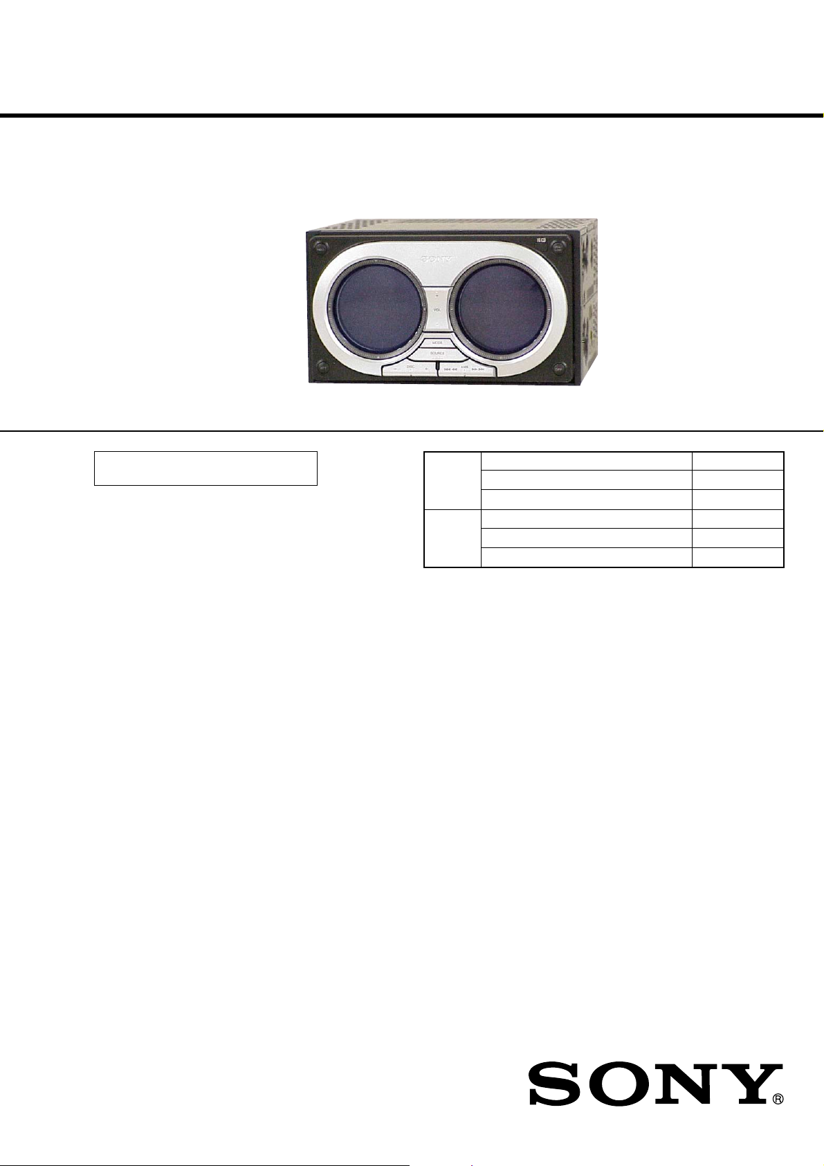
WX-7700MDX
SERVICE MANUAL
Ver 1.0 2002.06
US and foreign patents licensed from Dolby
Laboratories.
CD
Section
MD
Section
E Model
Model Name Using Similar Mechanism NEW
CD Mechanism Type MG-398D-121
Optical Pick-up Name KSS-720A
Model Name Using Similar Mechanism NEW
MD Mechanism Type MG-164MF-138
Optical Pick-up Name KMS-241C
CD/MD Player section
Signal-to-noise ratio 95 dB
Frequency response 10 – 20,000 Hz
Wow and flutter Below measurable limit
Tuner section
FM
Tuning range FM tuning interval:
Aerial terminal External aerial connector
Intermediate frequency 10.7 MHz/450 kHz
Usable sensitivity 8 dBf
Selectivity 75 dB at 400 kHz
Signal-to-noise ratio 66 dB (stereo),
Harmonic distortion at 1 kHz
Separation 35 dB at 1 kHz/WIDE
Frequency response 30 – 15,000 Hz
50 kHz/200 kHz switchable
87.5 – 108.0 MHz
(at 50 kHz step)
87.5 – 107.9 MHz
(at 200 kHz step)
74 dB (mono)
0.4 % (stereo),
0.3 % (mono)
SPECIFICATIONS
AM
Tuning range AM tuning interval:
Aerial terminal External aerial connector
Intermediate frequency 10.7 MHz/450 kHz
Sensitivity 30 µV
Power amplifier section
Outputs Speaker outputs
Speaker impedance 4 – 8 ohms
Maximum power outp ut 52 W × 4 (at 4 ohms)
General
Outputs Audio outputs (front/rear)
Inputs Telephone ATT control
9 kHz/10 kHz switchable
531 – 1,602 kHz
(at 9 kHz step)
530 – 1,710 kHz
(at 10 kHz step)
(sure seal connectors)
Subwoofer output (mono)
Power aerial relay control
terminal
Power amplifier control
terminal
terminal
Illumination control
terminal
BUS control input terminal
BUS audio input terminal
AUX IN terminal
Aerial input terminal
Power requirements 12 V DC car batt ery
Dimensions Approx. 178 × 100 × 194
Mounting dimensions Approx. 178 × 100 × 165
Mass Approx. 3.0 kg
Supplied accessories Parts for installation and
Note
This unit cannot be connected to a digital preamplifier
or an equalizer.
Design and specifications are subject to change
without notice.
(negative earth)
mm (w/h/d)
mm (w/h/d)
connections (1 set)
Card remote commander
RM-X110
9-874-054-01 Sony Corporation
2002F0500-1 e Vehicle Company
C 2002.06 Published by Sony Engineering Corporation
MULTI CONTROL AUDIO MASTER
Page 2
WX-7700MDX
NOTES ON HANDLING THE OPTICAL PICKUP BLOCK OR BASE UNIT
The laser diode in the optical pick-up block may suffer electrostatic breakdown because of the potential difference generated by
the charged electrostatic load, etc. on clothing and the human body .
During repair, pay attention to electrostatic breakdown and also
use the procedure in the printed matter which is included in the
repair parts.
The flexible board is easily damaged and should be handled with
care.
FOR CD
NOTES ON LASER DIODE EMISSION CHECK
The laser beam on this model is concentrated so as to be focused
on the disc reflective surface by the objective lens in the optical
pick-up block. Therefore, when checking the laser diode emission, observe from more than 30 cm away from the objectiv e lens.
FOR MD
NOTES ON LASER DIODE EMISSION CHECK
Never look into the laser diode emission from right avove when
checking it for adustment. It is feared that you will lose your sight.
NOTES ON HANDLING THE OPTICAL PICK-UP BLOCK
(KMS-241C)
The laser diode in the optical pick-up block may suffer electrostatic break-down easily. When handling it, perform soldering
bridge to the laser-tap on the flexible board. Also perform
m easur es against electrostatic break-down suff iciently before the
operation. The flexible board is easily damaged and should be
handled with care.
laser-tap
OPTICAL PICK-UP FLEXIBLE BOARD
Notes on chip component replacement
•Never reuse a disconnected chip component.
• Notice that the minus side of a tantalum capacitor may be damaged by heat.
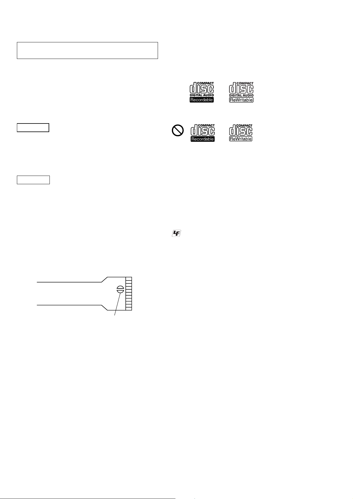
Notes on CD-R/CD-RW discs
•You can pl ay CD-Rs (recordabl e CD s)/CDRWs (rewritable CDs) designed for audio use
on this unit.
Look for these marks to distinguish CD-Rs/
CD-RWs for audio use.
These marks denote that a disc is not for audi o
use.
•Some CD-Rs/CD-RWs (depending on the
equipment used for its r ecording or the
condition of the disc) m ay not play on this unit.
•You cannot play a CD-R/a CD-RW that is not
finalized*.
*
A process necessary for a recorded CD-R/CD-RW
disc to be played on the audio CD player.
UNLEADED SOLDER
Boards requiring use of unleaded solder are printed with the leadfree mark (LF) indicating the solder contains no lead.
(Caution: Some printed circuit boards may not come printed with
the lead free mark due to their particular size)
: LEAD FREE MARK
Unleaded solder has the following characteristics.
• Unleaded solder melts at a temperature about 40 ˚C higher than
ordinary solder.
Ordinary soldering irons can be used but the iron tip has to be
applied to the solder joint for a slightly longer time.
Soldering irons using a temperature regulator should be set to
about 350 ˚C .
Caution: The printed pattern (copper foil) may peel away if the
heated tip is applied for too long, so be careful!
• Strong viscosity
Unleaded solder is more viscous (sticky , less prone to flow) than
ordinary solder so use caution not to let solder bridges occur
such as on IC pins, etc.
• Usable with ordinary solder
It is best to use only unleaded solder but unleaded solder may
also be added to ordinary solder.
Flexible Circuit Board Repairing
•Keep the temperature of the soldering iron around 270 ˚C during repairing.
• Do not touch the soldering iron on the same conductor of the
circuit board (within 3 times).
• Be careful not to apply force on the conductor when soldering
or unsoldering.
2
SAFETY-RELATED COMPONENT WARNING!!
COMPONENTS IDENTIFIED BY MARK 0 OR DOTTED
LINE WITH MARK 0 ON THE SCHEMATIC DIAGRAMS
AND IN THE PARTS LIST ARE CRITICAL TO SAFE
OPERATION. REPLACE THESE COMPONENTS WITH
SONY PARTS WHOSE PART NUMBERS APPEAR AS
SHOWN IN THIS MANUAL OR IN SUPPLEMENTS PUBLISHED BY SONY.
Page 3

TABLE OF CONTENTS
WX-7700MDX
1. SERVICING NOTES ................................................ 4
2. GENERAL
Location of Controls ....................................................... 5
3. DISASSEMBLY
3-1. Disassembly Flow........................................................... 10
3-2. Front Panel Section......................................................... 11
3-3. DISPLAY Board ............................................................. 11
3-4. Chassis (T) Section ......................................................... 12
3-5. MD Mechanism Deck (MG-164MF-138)...................... 12
3-6. POWER Board, Chassis (T) Assy .................................. 13
3-7. Heat Sink......................................................................... 13
3-8. SERVO (MD) Board ....................................................... 14
3-9. MD Cover Assy ............................................................... 14
3-10. Float Block ...................................................................... 15
3-11. LO Motor Assy................................................................ 15
3-12. Lever Assy (LE) .............................................................. 16
3-13. Holder Assy..................................................................... 16
3-14. Chucking ARM Assy ...................................................... 17
3-15. Optical Pick-up (KMS-241C)......................................... 17
3-16. SL Motor Assy (SLED) (M902)/
SP Motor Assy (SPINDLE) (M901)............................... 18
3-17. CD Mechanism Deck (MG-398D-121).......................... 18
3-18. Motor Assy (Front Panel Open/Close) (M640).............. 19
3-19. MAIN Board, Chassis (B) Assy ..................................... 19
3-20. Bracket (MAIN) .............................................................. 20
3-21. Chassis (T388) Assy ....................................................... 20
3-22. Sensor (CD) Board.......................................................... 21
3-23. Servo Board, LO Motor SUB Assy (Loading)
(M103)............................................................................. 21
3-24. ARM Roller Assy, LOAD Board.................................... 22
3-25. Floating Block Assy........................................................ 22
3-26. Optical Pick-up (KSS-720A), Sled Motor Assy
(M101)............................................................................. 23
5-20. Printed Wiring Boards
– DISPLAY Board (Conductor Side) – .......................... 43
5-21. Schematic Diagram – DISPLAY Board (1/2) – ............. 44
5-22. Schematic Diagram – DISPLAY Board (2/2) – ............. 45
5-23. Printed Wiring Board
– KEY Board (Component Side) –................................. 46
5-24. Printed Wiring Board
– KEY Board (Conductor Side) –................................... 47
5-25. Schematic Diagram – KEY Board – ............................. 48
5-26. Schematic Diagram – SUB/POWER Boards – ............. 49
5-27. Printed Wiring Board
– POWER Board (Component Side) – ........................... 50
5-28. Printed Wiring Boards – POWER Board
(Conductor Side)/SUB Board – ...................................... 51
5-29. IC Pin Function Description ........................................... 63
6. EXPLODED VIEWS
6-1. MAIN Section ................................................................. 78
6-2. SUB Panel SUB Assy Section ........................................ 79
6-3. Front Panel Section......................................................... 80
6-4. Front Panel SUB Section ................................................ 81
6-5. DISPLAY Board Section ................................................ 82
6-6. Chassis (T) Assy Section ................................................ 83
6-7. Chassis (B) Assy Section-1............................................. 84
6-8. Chassis (B) Assy Section-2............................................. 85
6-9. MD Mechanism Deck Section-1 (MG-164MF-138) ..... 86
6-10. MD Mechanism Deck Section-2 (MG-164MF-138) ..... 87
6-11. MD Mechanism Deck Section-3 (MG-164MF-138) ..... 88
6-12. CD Mechanism Deck Section-1 (MG-398D-121) ......... 89
6-13. CD Mechanism Deck Section-2 (MG-398D-121) ......... 90
6-14. CD Mechanism Deck Section-3 (MG-398D-121) ......... 91
7. ELECTRICAL PARTS LIST ............................... 92
4. ASSEMBLY
4-1. Assembly of ARM (L/R) Assy ....................................... 23
5. DIAGRAMS
5-1. Block Diagram – CD SERVO Section – ....................... 24
5-2. Block Diagram – MD SERVO Section – ...................... 25
5-3. Block Diagram – MAIN Section –................................ 26
5-4. Block Diagram
– DISPLAY/BUS CONTROL Section – ........................ 27
5-5. Block Diagram – POWER SUPPLY Section – ............. 28
5-6. Note for Printed Wiring Boards and
Schematic Diagrams ....................................................... 29
5-7. Printed Wiring Boards – CD Section (1/2) – ................ 30
5-8. Printed Wiring Board – CD Section (2/2) – .................. 31
5-9. Schematic Diagram – CD Section –.............................. 32
5-10. Printed Wiring Boards – MD Section –......................... 33
5-11. Schematic Diagram – MD Section (1/2) – .................... 34
5-12. Schematic Diagram – MD Section (2/2) – .................... 35
5-13. Printed Wiring Boards
– MAIN Board (Component Side) – .............................. 36
5-14. Printed Wiring Board
– MAIN Board (Conductor Side) – ................................ 37
5-15. Schematic Diagram – MAIN Board (1/4) – ................... 38
5-16. Schematic Diagram – MAIN Board (2/4) – ................... 39
5-17. Schematic Diagram – MAIN Board (3/4) – ................... 40
5-18. Schematic Diagram – MAIN Board (4/4) – ................... 41
5-19. Printed Wiring Board
– DISPLAY Board (Component Side) – ........................ 42
3
Page 4
WX-7700MDX
)
SECTION 1
SERVICING NOTES
TEST DISC
This set can playback a CD-R, CD-RW for audio use.
When test this set, use the following test disc.
Test disc for CD-R: TCD-R082LMT (Part No.: J-2502-063-1)
Test disc for CD-RW: TCD-W082L (Part No.: J-2502-063-2)
OPENING AND CLOSING OF FRONT PANEL SECTION IN AN ELECTRIC INTERRUPTION STATE
Don't apply impossible power, but open and close slowly with both hands.
front panel section
JIG ON REPAIRING
When repairing this set, etc., connect the extension cable as the figure shown below.
extension cable (main board-power board)
(J-2502-067-1)
CNP370
CN403
extension cable (main board-servo (CD) board
(J-2502-062-1)
CN331
CN1
4
Page 5
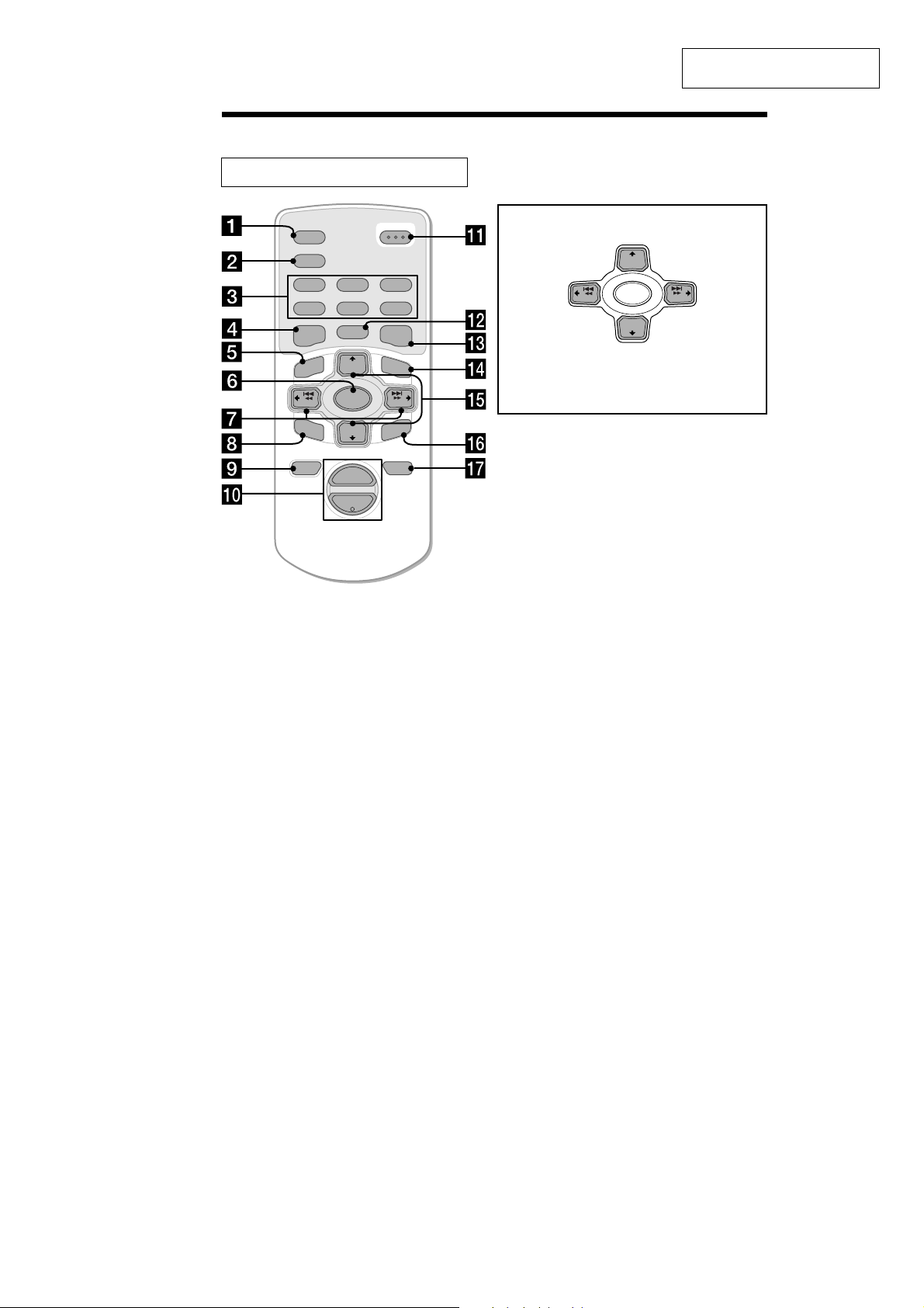
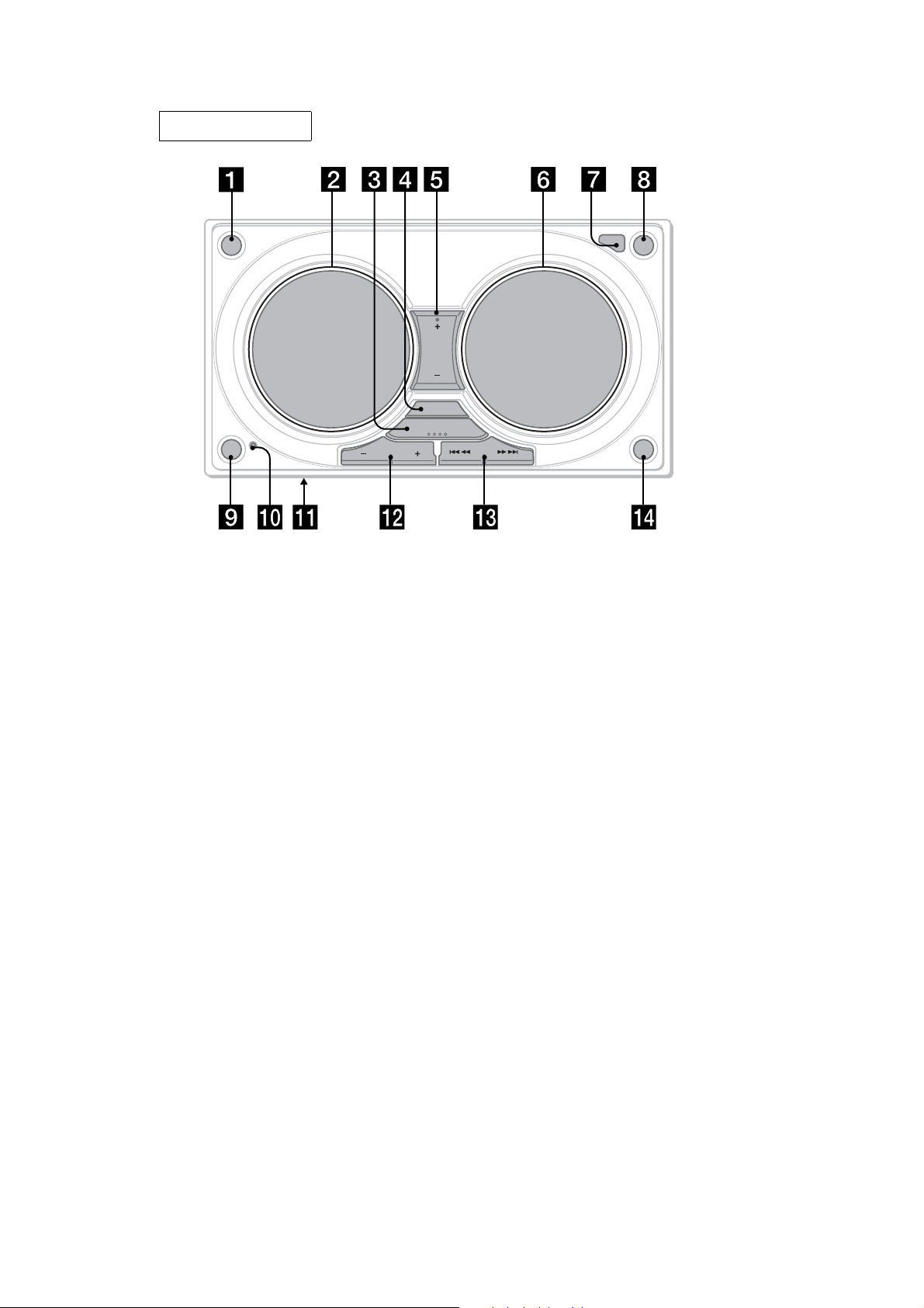
Location of controls
Card remote commander RM-X110
SECTION 2
GENERAL
WX-7700MDX
This section is extracted from
instruction manual.
2
5
MODE
+
DISC
SOURCE
–
DISC
+
VOL
OPEN/CLOSE
3
6
LIST
+
SEEK
ENTER
ATTOFF
SCRL
DSPL
REP SHUF
1
4
EQ7 DSO
MENU
–
SEEK
SOUND
–
Instructions in this manual describe how
to use the unit by mainly using the card
remote commander.
(DISC) (M):
to select upwards
+
DISC
(SEEK) (<):
to select
leftwards
In Menu mode, the currently selectable button(s) of
these four are indicated with a “ v” in the display.
Note
If the unit is turned off by pressing (OFF) for 2
seconds, the unit cannot be operated with the card
remote commander unless (SOURCE) on the unit is
pressed, or a disc is inserted to activate the unit first.
Tip
Refer to “Replacing the lithium battery” for details on
how to replace the batteries.
SOURCE
–
SEEK
–
DISC
(DISC) (m):
to select downwards
(SEEK) (,):
+
SEEK
to select
rightwards
a SCRL (scroll) button
b DSPL (display mode change) button
c Number buttons
(1) REP
(2) SHUF
To store station s/ r eceive stored stations.
d EQ7 button
e MENU button
To display the menus.
f SOURCE (Power on/Radio/CD/MD/
AUX-Audio) button
To select the source.
g SEEK (</,) buttons
To skip tracks/fast-f orward, reverse a track/
tune in stations automatically, find a station
manually/select a setting.
h SOUND button
i OFF (Stop/Power off) button
j VOL ( +/–) buttons
To turn up or down the volume.
k
OPEN/CLOSE button
l MODE button
To change the operation.
m DSO button
n LIST button
o DISC (M/m) buttons
To receive preset stations/change the disc*/
select an item in Menu.
* When an optional CD/MD unit is connected.
p ENTER button
To enter a setting.
q ATT button
5
Page 6
WX-7700MDX
Controls of the unit
ANGLE
ATT
DISC AMS
The buttons on the unit share the same
functions as those on the car d re mote
commander.
a ANGLE button
b Sound window
c SOURCE button
d MODE button
e VOL (+/–) button
f Operation window
g Receptor for the card remote
commander
h OPEN/CLOSE button
i ATT button
j Reset button
k Frequency select switch (located on the
bottom of the unit)
See “Frequency sel ect switch” in the
Installation/Con nections manual.
l DISC (–/+) button s
m AMS (. m/M >) buttons
AMS (. m/M >) buttons share
the same functions as SEEK (</,)
buttons on the card remote commander.
n OFF (Stop/Power off) button*
OPEN/
CLOSE
VOL
MODE
SOURCE
OFF
WX-7700MDX
* Warning when installing in a car without
an ACC (accessory) position on the
ignition switch
After turning off the ignition switch, be sure to
press (OFF) on the unit for 2 seconds to turn
off the clock display.
Otherwise, the clock display does not turn off
and this causes battery drain.
6
Page 7
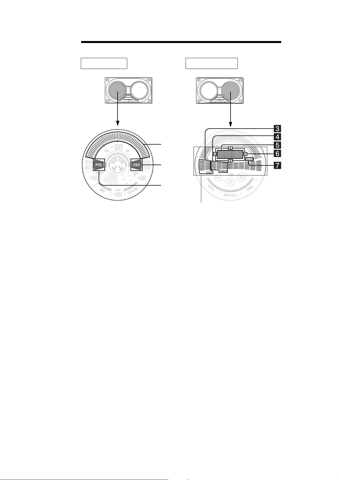
Display windows
Sound window Operation window
WX-7700MDX
ANGLE
VOL
MODE
SOURCE
DISC AMS
ATT
OPEN/
CLOSE
OFF
a DSO
Lights up while you are set t in g t he DSO
mode.
b POS
Lights up while you are set t in g t he POS
mode.
c DISC number
Appears only when an optional CD/MD unit
is connected and a disc in the optional un it is
played.
d Track number
Appears during CD/MD playback.
Level meter
(volume)
1
2
ANGLE
VOL
MODE
SOURCE
DISC AMS
ATT
This manual illustrates the
operation window mainly.
OPEN/
CLOSE
OFF
e Various items for a setting or a source
f Cursor directions
The selectable cu rsor direction appear s as a
“v”.
By pressing a cursor button (M/,/m/<) in
the same direction as any “v” that appears,
you can select an item or proceed with the
operation.
g
ENTER
Appears when it's necessary to press
(ENTER)
after you select an item.
7
Page 8

WX-7700MDX
2
SUBWOOFER OUT
A
(MONO)
AUDIO OUT
B
Source selector
XA-C30
(REAR)
BUS AUDIO IN
BUS CONTROL IN
*
AUDIO OUT
(FRONT)
BUS AUDIO IN
Cautions
• This unit is designed for negative earth 12 V
DC operation only.
• Do not get the wires under a screw, or caught
in moving parts (e.g. seat railing).
• Before making connections, turn the car
ignition off to avoid short circuits.
• Connect the yellow and red power input leads
only after all other leads have been connected.
• Run all earth wires to a common earth
point.
• Be sure to insulate any loose unconnected
wires with electrical tape for safety.
Notes on the power supply cord (yellow)
• When connecting this unit in combination with
other stereo components, the connected car
circuit’s rating must be higher than the sum of
each component’s fuse.
• When no car circuits are rated high enough,
connect the unit directly to the battery.
Parts Iist (1)
The numbers in the list are keyed to those in the
instructions.
Connection example (2)
Notes
(2-A)
• Be sure to connect the earth lead before
connecting the amplifier.
• If you connect an optional power amplifier and do
not use the built-in amplifier, the beep sound will
be deactivated.
Tip
(2-B- )
For connecting two or more changers, the source
selector XA-C30 (optional) is necessary.
Connection diagram (3)
When inserting each connector, be sure to insert
securely, as vibration through driving may
cause a poor connection.
1
To a metal surface of the car
Make sure to connect the black earth lead first of
all, then proceed with connection steps 2-7.
Check the black earth lead is connected properly,
before connecting the orange/white striped lead,
yellow and red power input leads.
2
To AMP REMOTE IN of an optional power
amplifier
This connection is only for amplifiers. Connecting
any other system may damage the unit.
3
To the power aerial control lead or power supply
lead of aerial booster amplifier
Notes
•It is not necessary to connect this lead if there
is no power aerial or aerial booster, or with a
manually-operated telescopic aerial.
•When your car has a built-in FM/AM aerial in
the rear/side glass, see “Notes on the control
and power supply leads.”
4
To the interface cable of a car telephone
5
To a car’s illumination signal
Be sure to connect the black earth lead to it first.
6
To the +12 V power terminal which is energized
in the accessory position of the ignition key
switch
Notes
• If there is no accessory position, connect to the
+12 V power (battery) terminal which is
energized at all times.
Be sure to connect the black earth lead to it
first.
•When your car has a built-in FM/AM aerial in
the rear/side glass, see “Notes on the control
and power supply leads.”
7
To the +12 V power terminal which is energized
at all times
Be sure to connect the black earth lead to it first.
Notes on the control and power supply leads
• The power aerial control lead (blue) supplies +12 V
DC when you turn on the tuner.
•When your car has built-in FM/AM aerial in the
rear/side glass, connect the power aerial control
lead (blue) or the accessory power input lead (red)
to the power terminal of the existing aerial
booster. For details, consult your dealer.
•A power aerial without relay box cannot be used
with this unit.
Memory hold connection
When the yellow power input lead is connected,
power will always be supplied to the memory circuit
even when the ignition key is turned off.
Notes on speaker connection
• Before connecting the speakers, turn the unit off.
• Use speakers with an impedance of 4 to 8 ohms,
and with adequate power handling capacities to
avoid its damage.
• Do not connect the speaker terminals to the car
chassis, or connect the terminals of the right
speakers with those of the left speaker.
• Do not connect the earth lead of this unit to the
negative (–) terminal of the speaker.
•Do not attempt to connect the speakers in parallel.
• Connect only passive speakers. Connecting active
speakers (with built-in amplifiers) to the speaker
terminals may damage the unit.
• To avoid a malfunction, do not use the built-in
speaker wires installed in your car if the unit shares
a common negative (–) lead for the right and left
speakers.
• Do not connect the unit’s speaker cords to each
other.
BUS CONTROL IN
*
not supplied
8
Page 9

WX-7700MDX
3
4
*
RCA pin cord
Left
Right
Left
SUBWOOFER OUT
(MONO)
1
*
BUS CONTROL IN
1
Supplied with XA-C30
*
AUX IN
2
*
3
4
Black
White
White/black striped
Grey
Grey/black striped
Green
Green/black striped
Fuse (10 A)
L
R
AUX IN
AUDIO OUT
(FRONT)
AUDIO OUT
(REAR)
L
R
REAR
Blue/white striped
Blue
Light blue
Orange/white striped
Red
Source selector
XA-C30
FRONT BUS AUDIO
AUDIO OUT IN
Supplied with the CD/MD changer
BUS AUDIO IN
RCA pin cord
*
Max. supply current 0.3 A
AMP REM
ANT REM
Max. supply current 0.1 A
ILLUMINATION
1
ATT
from car aerial
2
3
4
5
6
*1 not supplied
2
*
Connect the Bus cable to its
terminal with the unit’s V mark and
the Bus cable’s v mark aligned.
3
*
supplied with the auxiliary
equipment
4
*
Auxiliary optional equipment such
as portable DVD player (not
supplied)
4 A
TOYOTA/MITSUBISHI
This illustration is for TOYOTA cars.
1
or
2
max. size 5 × 8 mm
Precautions
• Choose the installation location carefully so
that the unit will not interfere with normal
driving operations.
• Avoid installing the unit in areas subject to
dust, dirt, excessive vibration, or high
temperatures, such as in direct sunlight or near
heater ducts.
• Use only the supplied mounting hardware for
a safe and secure installation.
To open/close the front panel smoothly, to insert/
eject a disc easily, and especially to drive safely, a
certain distance between the front panel and the
shift lever is necessary. The necessary distance
differs, depending on the shift lever position of
your car. Before installing the unit, choose the
installation location carefully so that you can
drive safely.
Shift lever
Mounting angle adjustment
Adjust the mounting angle to less than 30°.
88 mm
Right
Bracket
Existing parts supplied with your car
Purple
Purple/black striped
WX-7700MDX
to dashboard/centre console
Bracket
Frequency select switch
The AM (FM) tuning interval is factory-set to the
9 k (50 k) position. If the frequency allocation
system of your country is based on 10 kHz (200
kHz) interval, set the switch on the bottom of
the unit to the 10 k (200 k) position before
making connections.
After the frequency select switch is set, you must
press the reset button to reset the unit.
Yellow
B
NISSAN
1
or
max. size 5 × 8 mm
1
or
2
max. size 5 × 8 mm
Mounting the unit in a Japanese
car (4)
You may not be able to install this unit in some
makes of Japanese cars. In such a case, consult
your Sony dealer.
When mounting this unit to the preinstalled
brackets of your car, use the supplied screws 1
or 2 in the appropriate screw holes, according
to your vehicle: T for TOYOTA, M for
MITSUBISHI, and N for NISSAN.
Notes
• Use the screws 1 or 2 depending on the make of
•To prevent malfunction, be sure to install using
• Do not apply excessive force to the buttons of the
• Do not push on the display window.
• Before mounting, make sure there is nothing on
N
T
M
M
T
N
T
T
N
N
T
N
M
car. When this unit is attached to a MITSUBISHI car,
use the supplied screws 2.
brackets and the supplied screws 1 or 2.
unit.
the top of the unit.
7
2
Bracket
3
Existing parts supplied with your car
Warning when installing in a car
without ACC (accessory)
position on the ignition key
switch
Be sure to press (OFF) on the unit for two
seconds to turn off the clock display after
turning off the engine.
When you press (OFF) only momentarily, the
clock display does not turn off and this causes
battery wear.
WX-7700MDX
to dashboard/centre console
Bracket
Reset button
When the installation and connections are
completed, be sure to press the reset button with
a ballpoint pen, etc.
ANGLE
DISC AMS
ATT
Reset button
Note
When you connect the power supply cord to the
unit or reset the unit, wait for about 10 seconds
before you insert a disc. If you insert a disc within
these 10 seconds, the unit will not be reset, and you
will have to press the reset button again.
1
or
2
max. size 5 × 8 mm
VOL
MODE
SOURCE
OPEN/
CLOSE
OFF
9
Page 10
WX-7700MDX
• This set can be disassembled in the order shown below.
3-1. DISASSEMBLY FLOW
SECTION 3
DISASSEMBLY
SET
3-2. FRONT PANEL
SECTION
(Page 11)
3-4. CHASSIS (T) SECTION
(Page 12)
3-5. MD MECHANISM DECK
(MG-164MF-138)
(Page 12)
3-6. POWER BOARD,
CHASSIS (T)
ASSY
(Page 13)
3-7. HEAT SINK
(Page 13)
3-8. SERVO (MD)
3-9. MD COVER ASSY
3-10. FLOAT BLOCK
3-11. LO MOTOR ASSY
3-12. LEVER ASSY (LE)
Note 1: The process can be removed in every turn in the .
Note 2: Unless finishes all processes in the , it cannot progress to the following process.
3-3. DISPLAY BOARD
(Page 11)
3-17. CD MECHANISM DECK
(MG-398D-121)
(Page 18)
BOARD (Page 14)
(Page 14)
(Page 15)
(Page 15)
(Page 16)
3-18. MOTOR ASSY
(FRONT PANEL OPEN/
CLOSE) (M640)
(Page 19)
3-19. MAIN BOARD,
CHASSIS (B)
ASSY
(Page 19)
3-20. BRACKET
(MAIN)
(Page 20)
3-21. CHASSIS (T388)
ASSY
(Page 20)
3-23. SERVO (CD)
BOARD, LO
MOTOR SUB ASSY
(LOADING) (M103)
(Page21)
3-24. ARM ROLLER
ASSY,
LOAD BOARD
(Page 22)
3-22. SENSOR (CD)
BOARD (Page 21)
3-13. HOLDER ASSY
(Page 16)
3-14. CHUCKING ARM ASSY
(Page 17)
3-15. OPTICAL PICK-UP
(KMS-241C)
(Page 17)
3-16. SL MOTOR ASSY
(SLED) (M902)/
SP MOTOR ASSY
(SPINDLE) (M901)
(Page 18)
3-25. FLOATING BLOCK
ASSY
(Page22)
3-26. OPTICAL PICK-UP
(KSS-720A),
SLED MOTOR ASSY
(M101)
(Page23)
10
Page 11
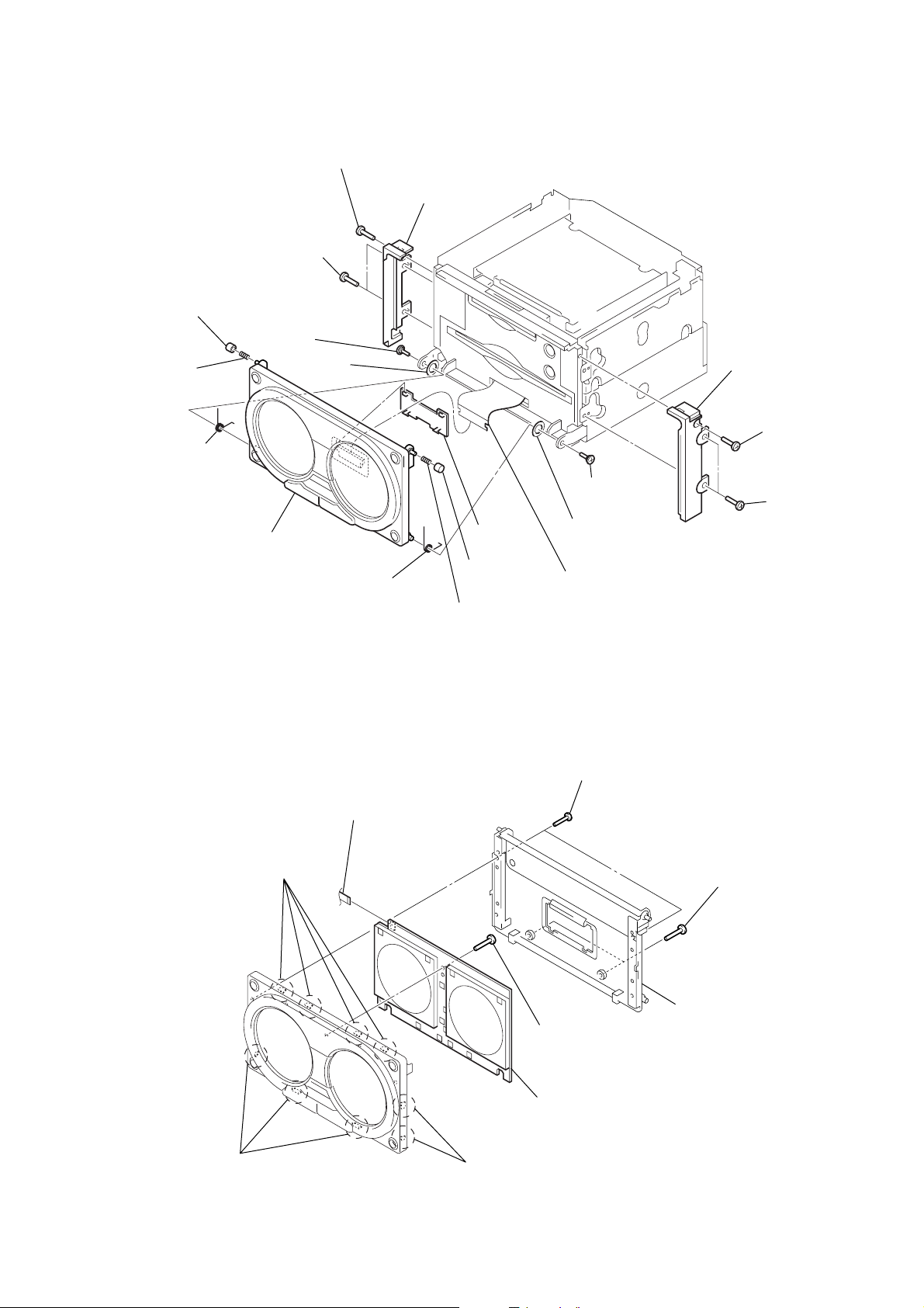
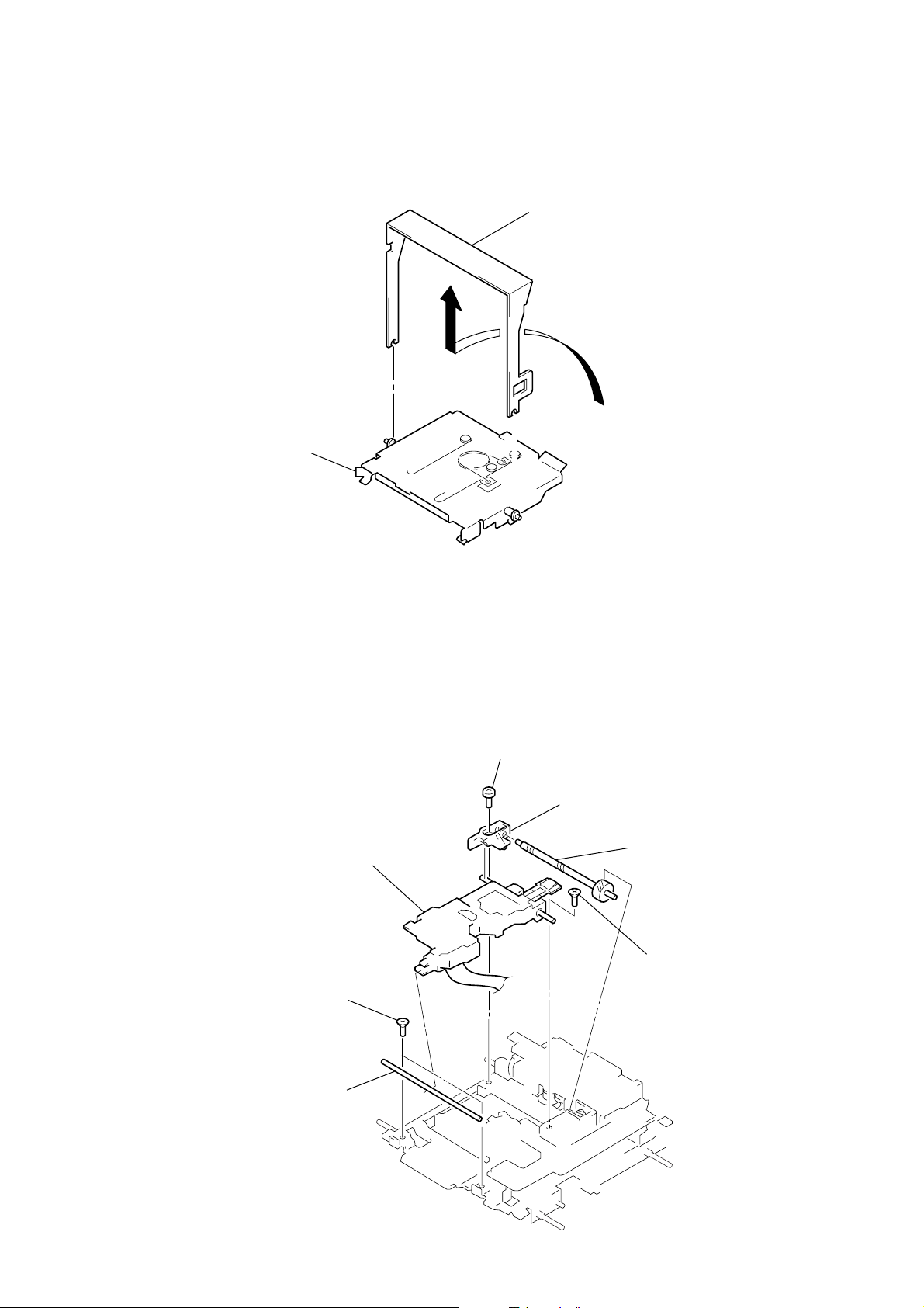
Note: Follow the disassembly procedure in the numerical order given.
w
3-2. FRONT PANEL SECTION
1
tapping screw
3
guide panel (L)
2
two screws
(PTT2.6 × 6)
4
roller
(guide)
5
spring
(guide)
8
torsion spring
(fulcrum: R)
qa
6
ornamental
screw
7
front panel section
8
sleeve
torsion spring
(fulcrum: L)
5
spring
(guide)
4
9
cover
(flexible)
roller
(guide)
6
ornamental
screw
7
sleeve
0
key connection
flexible board
WX-7700MDX
3
guide panel (R)
1
tapping scre
2
two screws
(PTT2.6 × 6)
3-3. DISPLAY BOARD
3
four claws
5
flaxible frat cable (7P)
(CN711)
1
two screws
(P2
×
6
tapping screws
7
display board
5)
2
two tapping screws
4
front back panel
3
three claws
3
two claws
11
Page 12
WX-7700MDX
n
3-4. CHASSIS (T) SECTION
3
two screws
(PTT2.6
×
6)
2
connector (CN400)
1
flexible flat cable (40P)
(CN403)
4
chassis (T) sectio
3
two screws
(PTT2.6
×
6)
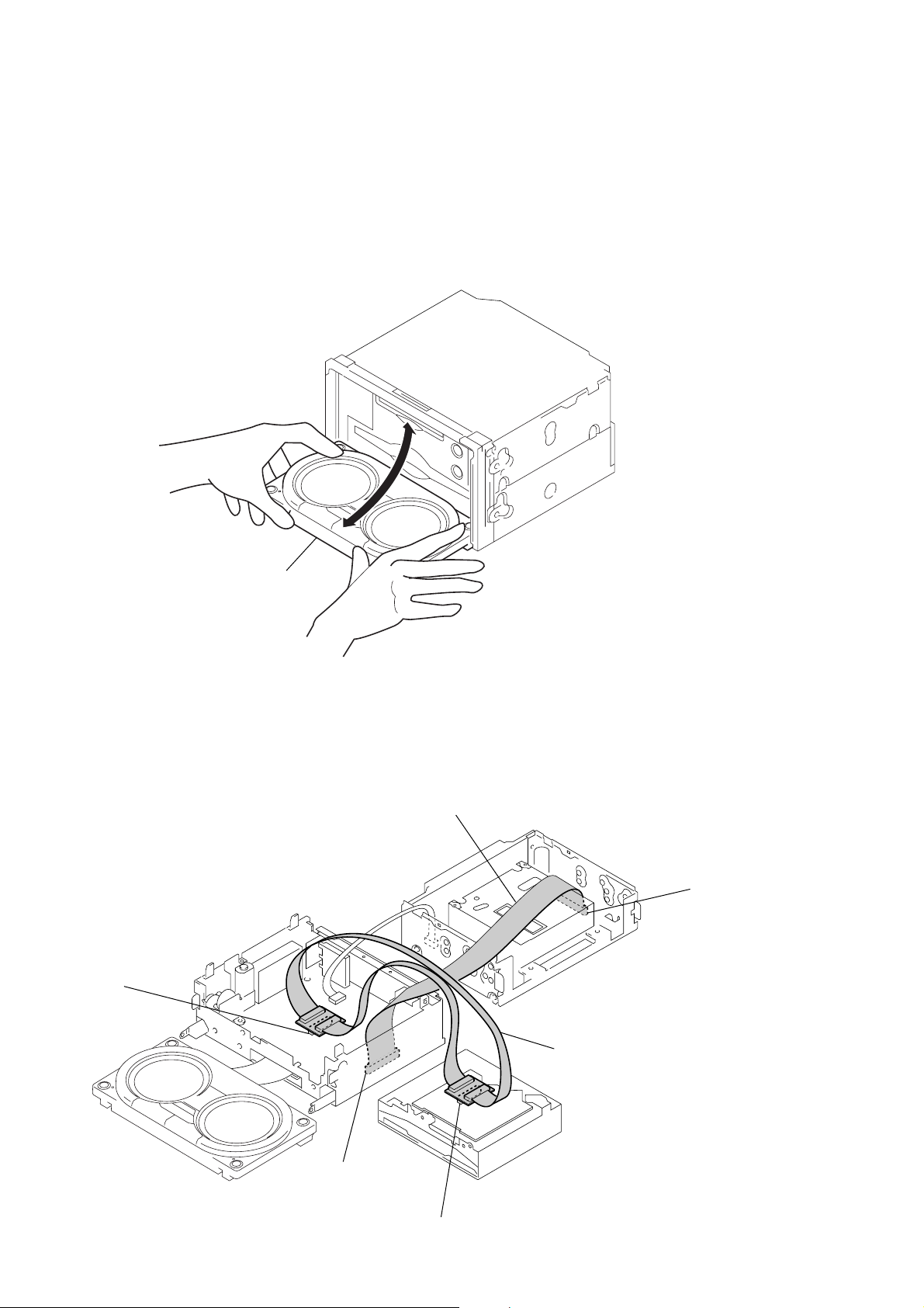
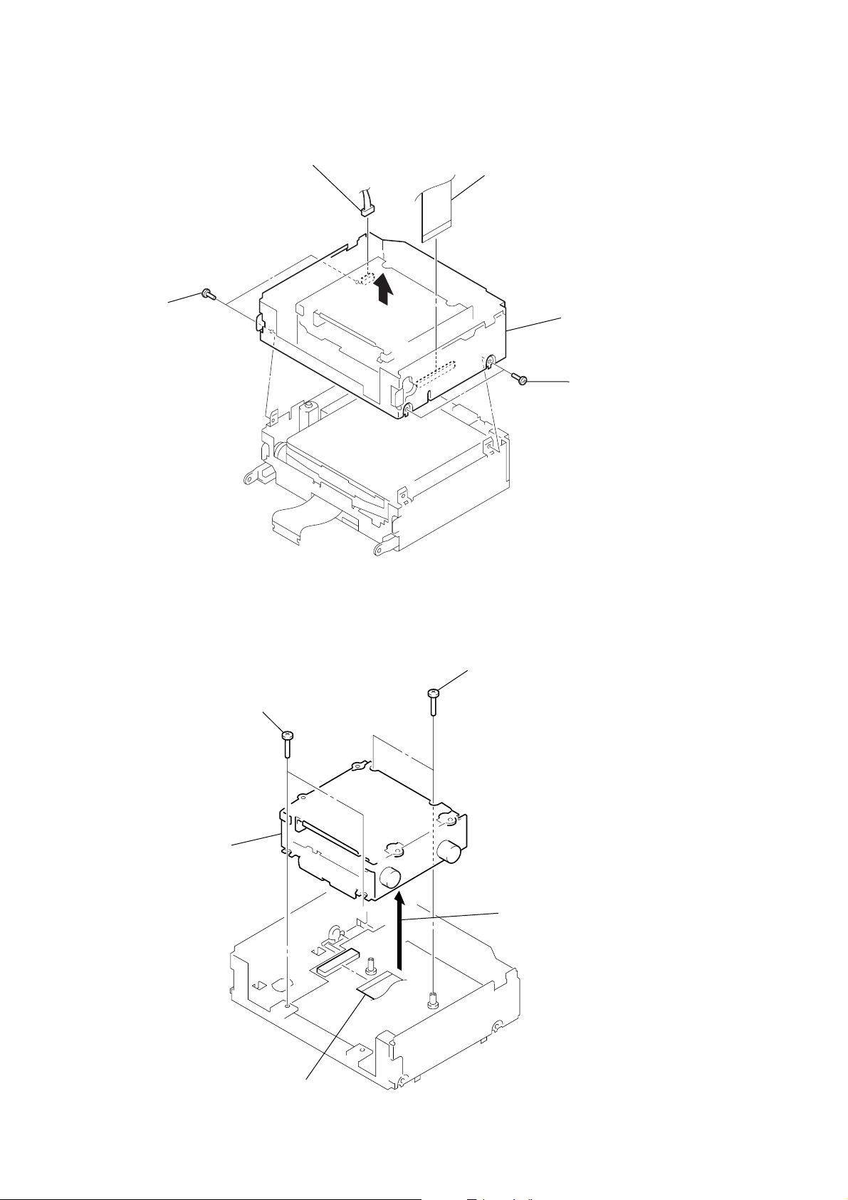
3-5. MD MECHANISM DECK (MG-164MF-138)
1
4
MD mechanism deck (MG-164MF-138)
two screws
(PTT2.6
×
5)
1
two screws
(PTT2.6
×
5)
2
Rifting up the MD mechanism deck.
12
3
flexible flat cable (30P)
(CN402)
Page 13

3-6. POWER BOARD, CHASSIS (T) ASSY
)
)
2
four ground point screws
3
power board
1
two screws
(PTT2.6 × 6
WX-7700MDX
4
chassis (T) assembly
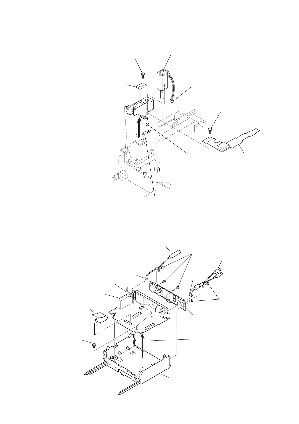
3-7. HEAT SINK
2
heat sink
1
four screws
(PTT2.6 × 10
power board
13
Page 14
WX-7700MDX
d
3-8. SERVO (MD) BOARD
2
two screws
(BVTT2 × 4)
1
sensor connection
flexible board
(CN103)
1
MD flexible board
(CN101)
2
two screws
(BVTT2 × 4)
3
servo (MD) boar
1
flexible board
(CN103)
3-9. MD COVER ASSY
3
MD cover assy
casset holder
ring (MD cover guide)
1
four screws
(B2
×
3)
14
A
2
Pushing the cassette holder in the direction of arrow A with a screwdriver,
disengage the shaft (MD cover guide) from the groove of MD cover ass’y.
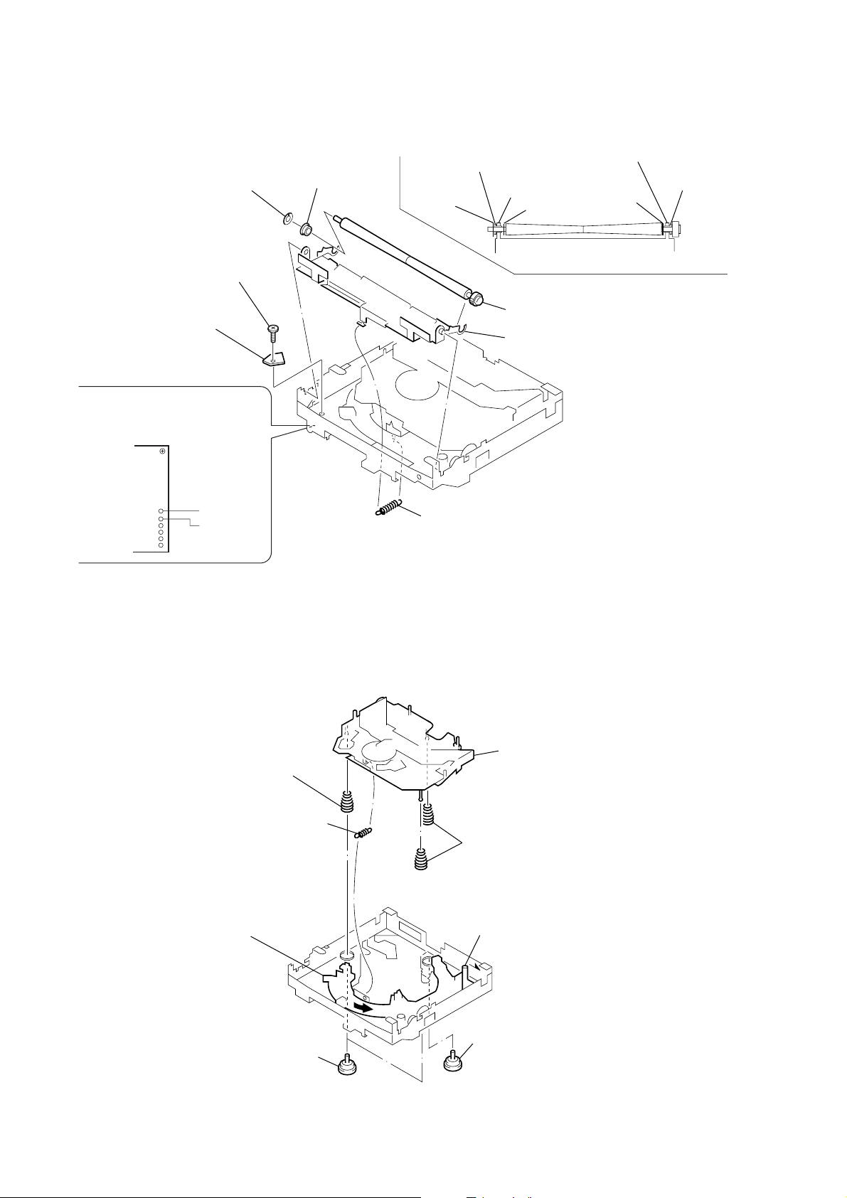
Note : Be careful not to damage the optical pick-up
when pushing the cassette holder with a screwdriver.
Page 15
3-10. FLOAT BLOCK
float block
A
3
Pushing an arrow A part, raise the float block
up ward at the front to release a lock.
1
tension spring (float B)
5
two damper assies
6
float block
WX-7700MDX
5
two damper assies
lock open
3-11. LO MOTOR ASSY
1
Remove solders of motor (M903)
lever (lock R)
lever (lock L)
2
two tension springs (float F)
4
Remove the bracket (LO)
in the direction of arrow
A
4
1
tension spring (float B)
.
5
A
LO motor ass’y (loading)
(M903)
2
tension spring (rack)
3
claw
– bottom view –
bracket (LO)
15
Page 16
WX-7700MDX
)
3-12. LEVER ASSY (LE)
2
stopper washer
1
3
4
roller (gear E)
lever (LE) ass’y
3-13. HOLDER ASSY
7
type-E stopring 1.5
4
spring (CHKG)
5
type-E stopring 1.5
6
lever (lock R)
8
Remove the holder ass’y in the
direction of the arrow.
7
type-E stopring 1.5
16
3
lever (lock L)
2
type-E stopring 1.5
1
spring (CHKG
Page 17
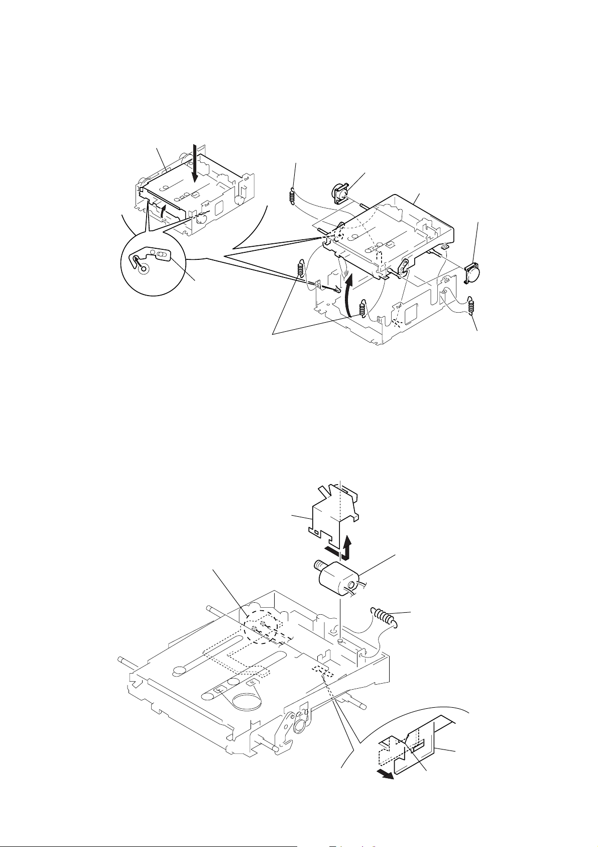
y
y
3-14. CHUCKING ARM ASSY
holder ass’y
1
Remove the chucking arm ass’
in the direction of the arrow.
WX-7700MDX
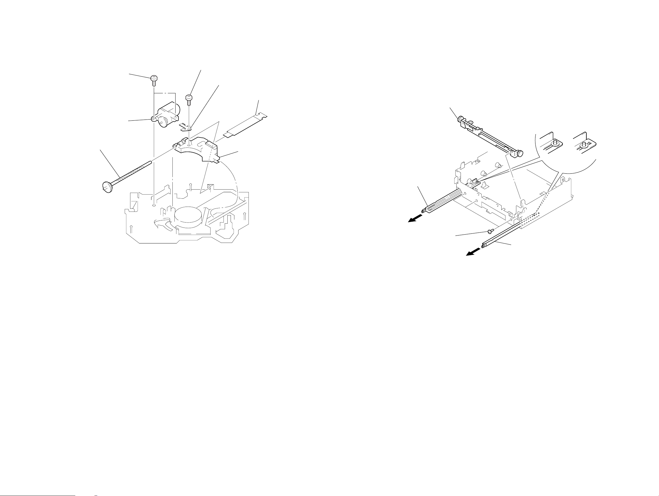
3-15. OPTICAL PICK-UP (KMS-241C)
7
optical pick-up (KMS-241C)
1
two screws
(K2 × 3)
2
guide shaft (OPT L)
4
screw
(B2 × 3)
6
bearing (SL)
5
feed screw ass’
3
screw
(K2 × 3)
17
Page 18

WX-7700MDX
)
3-16. SL MOTOR ASSY (SLED) (M902)/SP MOTOR ASSY (SPINDLE) (M901)
5
screw
×
1.8)
(P1.7
0
two screws
×
1.8)
qa
bracket (SP)
qs
SP motor ass’y
(spindle) (M901)
(P1.7
6
7
SL motor ass’y
(sled) (M902)
8
screw
×
(B2
9
base (SL)
bracket (SL)
3)
3
screw (PS2 × 8)
2
screw (PS2 × 4)
4
sensor (MD) board
3-17. CD MECHANISM DECK (MG-398D-121)
5
CD mechanism deck (MG-398D-121)
4
bracket (CD)
1
two screws
(PTT2.6
2
1
Remove solders of motors
(M901, M902)
×
6)
3
connector
(CNP370)
two screws
(PTT2.6
×
6
18
1
two screws
(PTT2.6
×
6)
Page 19
2
two screws
(PTT2.6
×
6)
2
four screws
(PTT2.6
×
6)
8
cord (with connector) (RCA)
qa
cord (with connector)
(ANT)
0
connector
(CN1)
9
Remove a solder of earth wire.
qs
main board
1
key connection flexible board
(CN670)
4
ground point screw
5
Remove the main board
from the chassis (B) assy.
6
chassis (B) assy
3
rear panel
7
connector
(CN3)
3-18. MOTOR ASSY (FRONT PANEL OPEN/CLOSE) (M640)
8
motor assy (front panel open/close) (M640)
5
Remove the bracket (motor) assy
in the direction of arrow.
4
two screws
(PTT2.6 × 6)
1
connector
(CN640)
7
two screws
(P2 × 2.5)
2
ground point screw
WX-7700MDX
3
heat sink
3-19. MAIN BOARD, CHASSIS (B) ASSY
6
harness
19
Page 20
WX-7700MDX
)
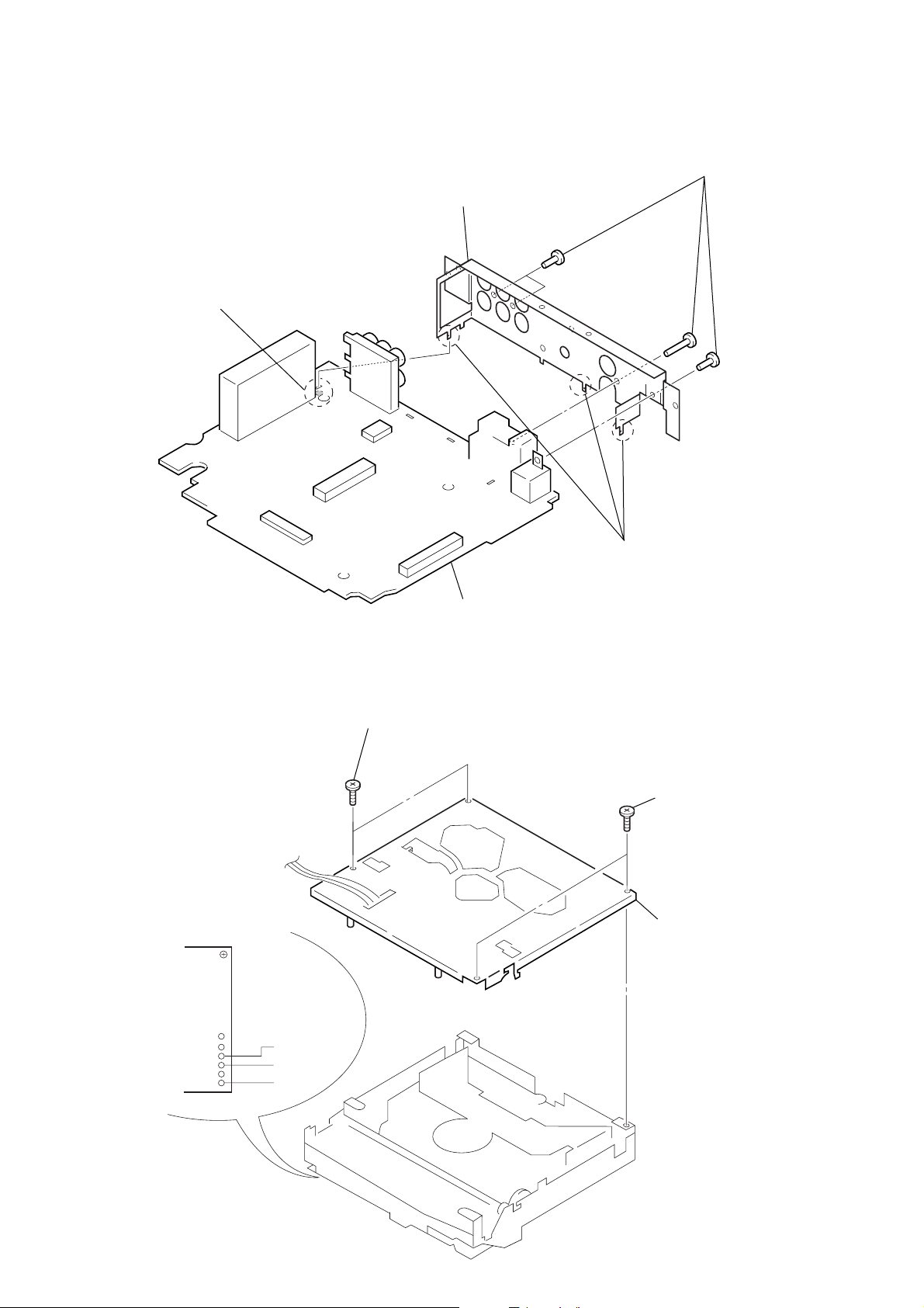
3-20. BRACKET (MAIN)
2
Remove a solder of bracket (main).
4
bracket (main)
1
four screws
(PTT2.6
×
6
3-21. CHASSIS (T388) ASSY
1
Remove three solders
of lead wire from sensor board.
2
two screws
(PTT2
×
3)
main board
3
Bend three claws.
3
two screws
(PTT2
4
chassis (T388) assy
×
3)
20
black
blue
red
Page 21
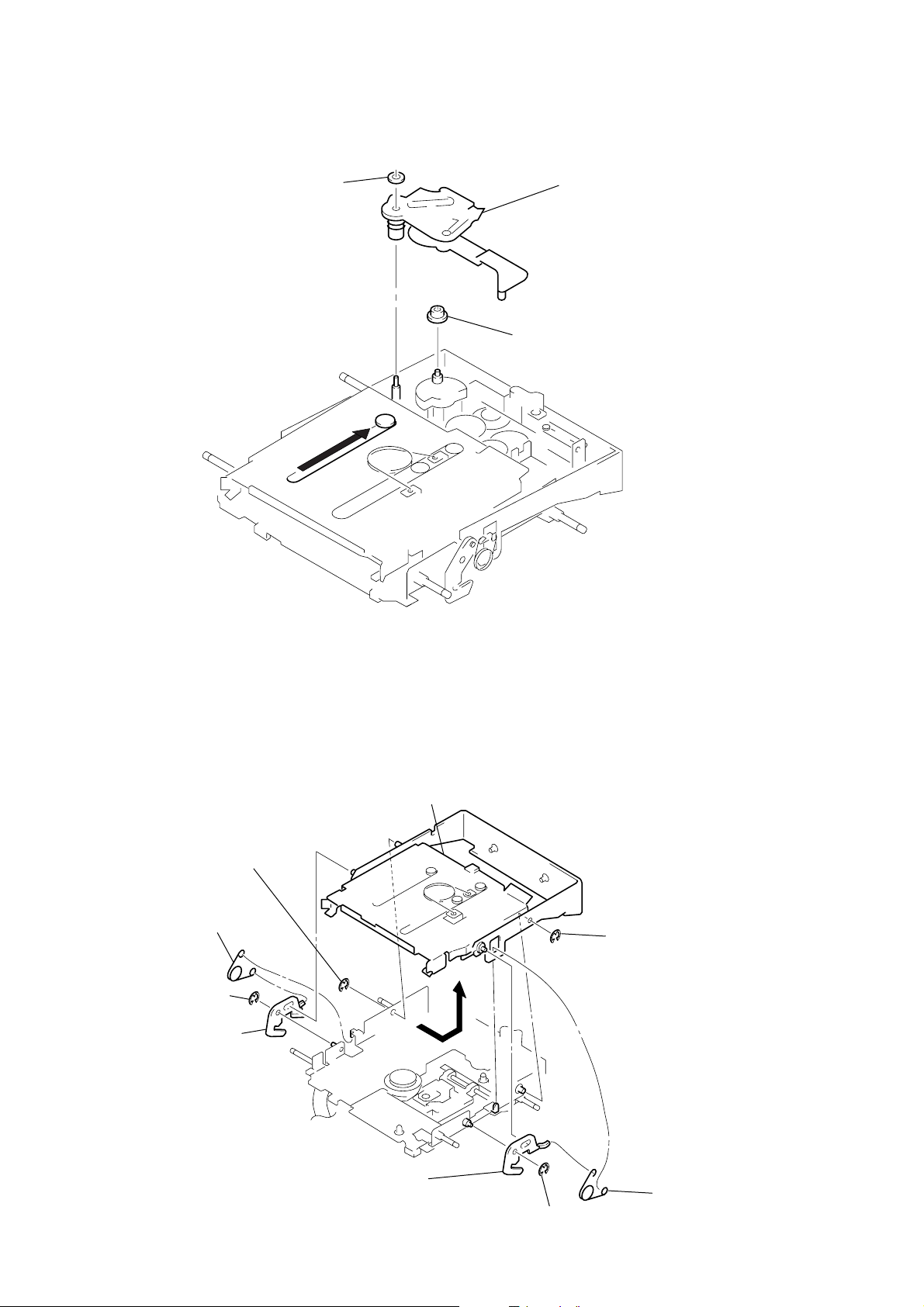
d
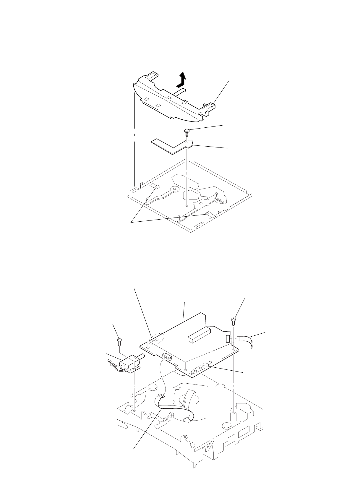
3-22. SENSOR (CD) BOARD
WX-7700MDX
two claws
1
2
3
guide (disc M)
4
special screw
5
sensor (CD) boar
3-23. SERVO BOARD, LO MOTOR SUB ASSY (LOADING) (M103)
2
Remove two solders of lead wire
of loading motor.
4
servo board
5
screw
×
3)
(P2
6
LO motor sub assy
(loading) (M103)
3
three screws
(PS2
2
×
4)
1
pick-up flexible board
(CN2)
Remove five solders of lead wire
of sensor board and load board.
1
motor frexible board (CN3)
21
Page 22
WX-7700MDX
3-24. ARM ROLLER ASSY, LOAD BOARD
3
retaining ring
(RA)
7
special screw
8
load board
6
Remove two solders of lead wire
from load board.
yellow
black
4
shaft retainer
(roller)
shaft retainer (roller)
retaining ring
(RA)
1
tension spring (RA)
arm (roller)
washer
5
arm roller assy
2
arm (roller)
arm (roller)
shaft retainer
(roller)
washer
3-25. FLOATING BLOCK ASSY
8
compression spring
(FL)
1
tension spring (KF1)
5
Turn loading ring in the direction of arrow.
3
damper (T)
6
floating block assy
7
compression spring
(FL)
4
Slide the lever (D) in the direction of arrow.
2
damper (T)
22
Page 23
)
SECTION 4
PHASE ALIGNMENT
WX-7700MDX
3-26. OPTICAL PICK-UP (KSS-720A), SLED MOTOR ASSY (M101)
1
2
sled motor assy
(M101)
7
shaft (feed) assy
two screws
(PS2
×
3)
5
two screws (PS2 × 3)
6
plate spring (feed)
4
pick up flexible board
3
optical pick-up (KSS-720A
Note: Follow the assembly procedure in the numerical order given.
4-1. ASSEMBLY OF ARM (L/R) ASSY
2
drive shaft assy
1
Pull the arm (L) assy
in the direction of arrow
at the full.
OK NG
3
three screws
(PS2.6 × 4)
1
Pull the arm (R) assy in the direction of arrow
at the full.
2323
Page 24
WX-7700MDX
SECTION 5
DIAGRAMS
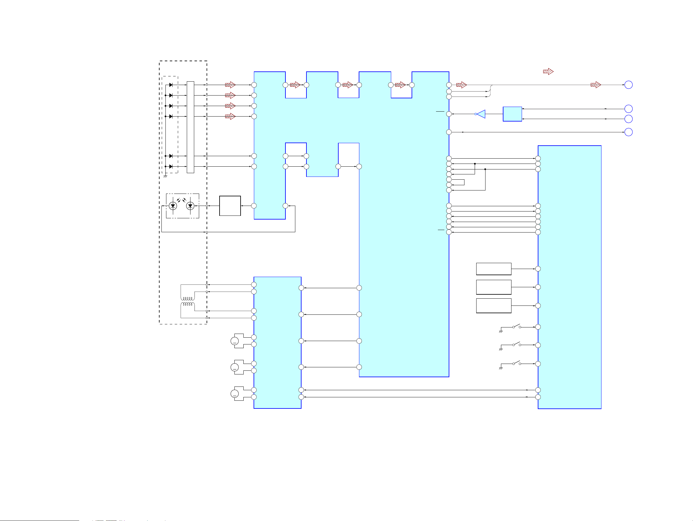
5-1. BLOCK DIAGRAM – CD SERVO Section –
DETECTOR
A
B
C
D
I-V AMP
A
B
C
D
B
84
A
82
D
85
C
83
RFO
77
AGCI
76
RF AMP,
FOCUS/TRACKING ERROR AMP,
DIGITAL SIGNAL PROCESSOR,
DIGITAL SERVO PROCESSOR,
DIGITAL FILTER, D/A CONVERTER.
CD-TEXT
IC1
AGCO
• SIGNAL PATH
: CD PLAY
EFM
75
RFI
74
71
ASY
72
DOUT
SCKO
LRCK
XTAL
EMPH
30
32
34
24
27
CD-DATA
CD-BCK
CD-LRCK
IC3
CD CLOCK
SWITCH
IC503
CD-DATA,
CD-BCK,
CD-LRCK
BFOT
CDM ON
CD EMPH
A
B
C
D
(Page 26)
(Page 26)
(Page 28)
(Page 26)
E
F
LASER DIODE
PICK-UP BLOCK
(KSS-720A)
2-AXIS DEVICE
(FOCUS)
(TRACKING)
PD LD
OPTICAL
PD
FCS+
FCS–
TRK+
TRK–
E
F
LD
AUTOMATIC
POWER
CONTROL
M101
(SLED)
Q1
M
87
86
98
LD
FOCUS/TRACKING COIL DRIVE,
16
15
17
18
14
13
FEO
E
F
SLED/SPINDLE/LOADING
VO4–
VO4+
VO3+
VO3–
VO1+
VO1–
91
TEO
93
97
PD
MOTOR DRIVE
IC2
OPIN4–
OPIN3–
IN1
FE–
90
TE2
TE–
92
26
23
5
94
TEC
95
FD
62
TD
63
SD
64
SCK
TSI
TSO
TSOI
TSCK
RFOK
PACK
STB
TSTB
RST
7
SO
8
SI
6
54
53
39
55
2
52
5
56
4
A0
3
DISC IN DETECT
D12, Q6
DISC SIZE
(8cm/12cm) DETECT
D11, Q7
LOADING
COMPLETION DETECT
D10, Q8
SW3
(DISC SET)
SW1
(SELF)
CD SI/TSI
25
CD SO/TSO
26
CD CKO/TCKO
27
CD RFOK
59
CD PACK
64
CD STB
37
CD TSTB
41
CD A0
36
CD XRST
35
MASTER CONTROLLER
(CD MECHANISM CONTROLLER)
IC550 (1/4)
CD PH1
60
CD PH2
66
CD PH3
61
CD DSW
62
CD SELFSW
67
M102
(SPINDLE)
M103
(LOADING)
11
M
M
VO2–
12
VO2+
10
VOL+
9
VOL–
FWD
REV
IN2
6
1
2
MD
65
SW4
(LIMIT)
68
57
58
CD LIMIT
CD LM LO
CD LM EJ
2424
Page 25
5-2. BLOCK DIAGRAM – MD SERVO Section –
OPTICAL PICK-UP BLOCK
(KMS-241C)
F
C B
I J
A
D
E
DETECTOR
LDPD
LASER DIODE
ILCC
I
J
B
A
C
D
E
F
RM
AUTOMATIC
POWER CONTROL
Q302
48 47
MORFI
MORFO
I
1
RF AMP
J
2
A
4
B
5
I-V
C
AMP
6
D
7
E
8
I-V
F
AMP
9
APC
LD/PD
11
10
AMP
PD
RFO
46 40
B.P.F.
3T
TEMP
WBL
AT
B.P.F.
AMP
ABCD
AMP
COMMAND
SERIAL/PARALLEL
CONVERTER,
DECODER
APCREF
12
SWDT
EFM/ACIRC ENCODER/DECODER,
SHOCK PROOF MEMORY CONTROLLER,
FOCUS/TRACKING ERROR AMP
AGCI
WBL
PEAK &
BOTTOM
ADFM ADIN
SCLK
181716
FOCUS
ERROR AMP
TRACKING
ERROR AMP
XLAT
3029
EQ
CONVERTER
DIGITAL SIGNAL PROCESSOR,
ATRAC ENCODER/DECODER
IC301 (1/2)
RF AMP,
IC302
RF
V-I
RF AGC
& EQ
EQ
3T
WBL
AUX
PEAK
BOTM
ADFG
ABCD
F0CNT
38
33
37
36
32
35
FE
34
TE
26
SE
28
20
FILTER
100
60
59
62
61
53
54
57
78
79
EFMO
FILI
PCO
CLTV
FILO
ASYO
ASYI
RFI
ADFG
F0CNT
PLL
COMPA-
RATOR
ADIP
DEMODULATOR/
DECODER
+3.3V
SPINDLE
SERVO
SPFD
94 93
PROCESSOR
SPRD
15
EFM/ACIRC
ENCODER/DECODER
SUBCODE
DQSY11SQSY14XINT
12
LEVEL SHIFT
IC502 (1/2)
TX
SHOCK PROOF
MEMORY CONTROLLER
CPU
INTERFACE
SENS
SRDT
SWDT
9 8 5 6 7
17
111315
975
3
SAMPLING
CONVERTER
ATRAC
DIGITAL
AUDIO
INTERFACE
ENCODER/DECODER
INTERNAL BUS
SCLK
XLAT
RATE
MONITOR
CONTROL
MNT0
MNT1
1 2 3 4
246
LEVEL SHIFT
IC502 (2/2)
181614
ADDT
DATAI
XBCKI
LRCKI
DIN0
DIN1
DOUT
DADT
MNT2
MNT3
8
12
WX-7700MDX
• SIGNAL PATH
: MD PLAY
25
22
24
23
19
20
21
MD-DATA, MD-BCK, MD-LRCK
DIVIDER
IC304
512FS
E
F
(Page 26)
(Page 26)
28
2927
LRCK
XBCK
FS256
CLOCK
GENERATOR
MD-DATA
MD-BCK
MD-LRCK
OSCI
OSCO
XOE
XWE
XRAS
XCAS
16
17
D0 – D3A00 – A09
49, 48, 50, 5134 – 31, 36 – 40, 45
43
47
46
44
DELAY BUFFER
IC306
D0 – D3
1, 2, 24, 25
D-RAM
IC307
A00 – A09
9 – 12, 14 – 18, 5
22
OE
3
WE
RAS
4
CAS
23
26
2-AXIS
DEVICE
(TRACKING)
FCS+
(FOCUS)
FCS–
TRK+
TRK–
FOCUS/TRACKING COIL DRIVE,
SPINDLE/SLED MOTOR DRIVE
IC303
M901
M902
(SLED)
MM
M
(SPINDLE)
FOK
SLOCK
XBUSY
TH501
X501
10MHz
Q301
ABCD
FE
AUX1
ABCD
ANALOG MUX
A/D CONVERTER
FROM CPU
INTERFACE
AUTO
SEQUENCER
3159
32 2664 27 28 2945
XTAL
EXTAL
MD-RST
TE
SE
PEAK
BOTM
XLRF
80
CKRF
81
DTRF
82
EJECT
LOAD
7 6
5 4
FIN
RIN
LOADING
MOTOR DRIVE
IC305
OUT1
OUT2
1 7
62 55 5254 51
39
SQSY
TEMP
6
VREF
SENS
CC-XINT
LIMIT-IN
(LIMIT)
REFERENCE VOLTAGE
REGULATOR
Q303
M
M903
(LOADING)
PEAK HOLD
16
PSB
OUT4F
6
OUT4R
8
OUT2F
27
OUT2R
25
OUT1F
21
23
OUT1R
OUT3F
12
10
OUT3R
IN4R
IN4F
IN2F
IN2R
IN1F
IN1R
IN3F
IN3R
SPFD
3
SPRD
4
29
30
19
18
14
15
83 13 67 65 66 75 74 63 64
10
XRST
APCREF
SFDR
92
SRDR
91
FFDR
88
FRDR
89
86
85
PWM GENERATOR
TFDR
TRDR
RECP
AUTOMATIC
POWER
CONTROL
DIGITAL SERVO
SIGNAL
PROCESS
DIGITAL SERVO
SIGNAL PROCESSOR
IC301 (2/2)
MD-SI
SCLK
SWDT
MD-SO
E-SW
LOADING
END
XLAT
MD-CKO
SHOCK
MNT0
MNT1
MNT2
MD-LAT
MD MECHANISM CONTROLLER
C-SW
631156
LOADING START/
LO +12V
MNT3
IC501 (1/2)
EJECT END
DEEMP
MDM-ON
MD-ON
66
10
65
MD EMPH
MD-ON, MDM-ON
G
H
(Page 26)
(Page 28)
2525
Page 26
WX-7700MDX
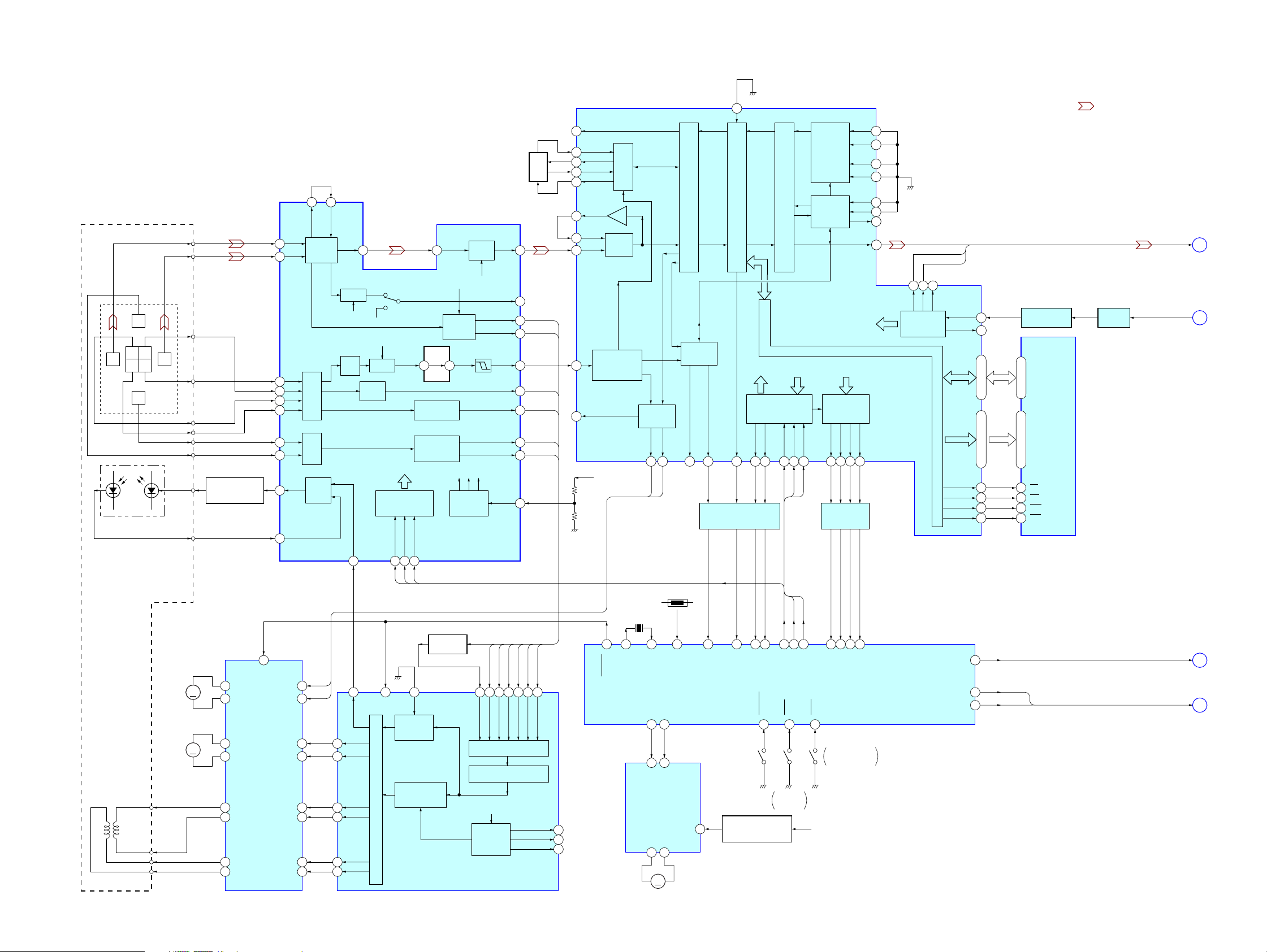
5-3. BLOCK DIAGRAM – MAIN Section –
A
(Page 24)
(Page 25)
E
(Page 24)
B
F
(Page 25)
BUS AUDIO
J
(Page 27)
CD-DATA,
CD-BCK,
CD-LRCK
MD-DATA,
MD-BCK,
MD-LRCK
BFOT
512FS
PNJ2
AUX IN
PNJ1 (1/2)
IN
ANT
SP SI,
SP CLK
R-CH
DSP +3.3V
(FOR DIGITAL)
77
XMST
71
SI1
75
BCK
76
LRCK
35
LIN
46
RIN
58
BFOT
81
PLCKL
FD2L+
7
FD1L+
3
AM
11
AMIF
12
MPX
13
DIGITAL SIGNAL PROCESSOR,
DIGITAL FILTER,
D/A CONVERTER
IC500
XLAT
RVDT59SCK
62 57
XLAT
SCK
RVDT
IC300 (1/2)
LOUDNESS/
VOLUME
PLL
REDY
6061
REDY
CANCELATION
TRDT
63
TRDT
INPUT SELECTOR, FM MPX
INPUT
MULTIPLEXER
AM/FM
NOISE
BLANKER
L.P.F.
11 10
EE SIO
EE CKO
XRST
DSPRST
PILOT
PILOT
DET
AOUTL1
AOUTR1
AOUTR3
AOUTL3
AOUTR2
XTLI38
XTLO38
XECKSTP64XS24
82
XECSKTP
27
29
54
52
43
41
40
SOFT
MUTE
QUAL
QUALITY
17
FL-OUT
RL-OUT
FR-OUT
R-CH
RR-OUT
R-CH
SUB-OUT
X500
16.9344MHz
TONE
CONTROL
LOUDNESSMUTE
DEMODULATOR
+STEREO ADJUST
+STEREO BLEND
MULTIPATH
DETECTOR
MPOUT16MPIN
15
53
VSM
LOW-PASS
FILTER
IC200
LOW-PASS
FILTER
IC101
OUTPUT
SELECTOR
L.P.F.
CONVERTER
R-CH
ACOUTL
38
TO
S & H HIGH-CUT
D/A
LEVEL
14
ACINLF
34
ACINLR
33
SWINL
36
35
SWINR
DIGITAL
CONTROL
IIC BUS
SDA
20
70 71
I2CSIO
R-CH
SCL
21
SM
I2CCKO
OUTPUT
18
ELECTRICAL VOLUME
IC300 (2/2)
MONO FADER MIXER
SELECTOR
SUBWOOFER
+PHASE CONTROL
XMST
TRDT
RVDT
SCK
XLAT
REDY
DSPRST
XECKSTP
SP SI
SP CLK
(CD MECHANISM CONTROLLER)
OUTLF
OUTLR
OUTSWL
MONO
OUTSWR
FADER
7
D AUDSEL
31
VOLATT
DSPMST
29
20
DSPSI
DSPSO
21
22
DSPCKO
DSPLAT
3
76
DSPREDY
4
DSPRST
28
DSPPLL
MASTER CONTROLLER
IC550 (2/4)
30
29
26
25
AMPON
TESTIN
TELMUTE
BEEP
R-CH
FL
K
(Page 27)
PNJ1 (2/2)
LINE
AMP
IC102
LINE
AMP
IC104
R-CH
LOW-PASS
FILTER
IC103
BZ300
BUZZER
DRIVE
Q307
15
120
84
16
115EMPH IN
LEVEL SHIFT
Q310
• R-ch is omitted due to same as L-ch.
MUTING
Q104
MUTING
Q203
MUTING
Q103
CENTER VOLTAGE
GENERATOR
(FOR BIAS)
IC303
MUTING
Q100
R-CH
MUTING
Q201
R-CH
BATTERY OFF
MUTE DRIVER
Q306
AUDIO +8V
FL
IN1
11
FR
12
IN2
RL
13
IN3
RR
IN4
14
MUTE
22
ST-BY
4
D304
MUTING CONTROL
MUTING CONTROL
R-CH
R-CH
R-CH
POWER AMP
IC402
BATT B+
SWITCH
Q305
SWITCH
Q303
D371
OUT1+
OUT1–
OUT2+
OUT2–
OUT3+
OUT3–
OUT4+
OUT4–
• SIGNAL PATH
: CD PLAY
D552
9
7
5
3
17
19
21
23
(L)
FRONT
(R)
(L)
REAR
(R)
(L)
SUB WOOFER
OUT (MONO)
(R)
CNP400 (1/2)
MUTE
CD EMPH
MD EMPH
AUDIO OUT
2
1
3
4
10
9
11
12
13
TEST
14
ATT
(Page 27)
(Page 24)
(Page 25)
FL+
FL–
FR+
FR–
RL+
RL–
RR+
RR–
L
D
G
: MD PLAY
: FM
: AM
B+ SWITCH
CD/MD
SELECTOR
IC504
MPX
16
11
3A
VCC
10
3B
2
1A
3
1B
5
2A
6
2B
SEL
8
10
12
13
17
18
14
CD-DATA
MD-DATA
CD-BCK
MD-BCK
CD-LRCK
MD-LRCK
(L)
(R)
(L)
(R)
R-CH
R-CH
AM ANT IN
1
2
FM ANT IN
TUNER UNIT
TU1
DAT-EEP
CKL-EEP
S-METER
AM DET
DAT IIC
CKL IIC
Q501
9
3Y
4
1Y
7
2Y
1
XMST
: BUS AUDIO IN
: AUX IN
2626
Page 27

WX-7700MDX
5-4. BLOCK DIAGRAM – DISPLAY/BUS CONTROL Section –
(Page 26) (Page 28)
FL
K
ILLON
M
LIQUID CRYSTAL
DISPLAY
LCD740
LIQUID CRYSTAL
DISPLAY
LCD741
BACK UP +5V
BACK UP +5V
FRONT PANEL
OPEN/CLOSE MOTOR DRIVE
IC641
M
M640
FRONT PANEL
OPEN/CLOSE
3
14
82-87, 91-101, 110-132
1-12, 18, 45, 51-53, 62-78,
54-61
79-81, 88-90
13-17, 19-25, 46-50,
133-140
53-80, 105-140
1-8
RESET SIGNAL
GENERATOR
IC551
RESET SIGNAL GENERATOR
(FOR INTERNAL RAM)
IC552
12
45
VCC
MOTOR
DRIVE
M BATT
OUT1
OUT2
SW800
(RESET)
VOLTAGE SWITCH
VREF
OPEN
CLOSE
RNF
SEG1 – SEG15,
SEG17 – SEG75
1 – 15, 17 – 75
83 – 76
COM1 – COM8
LIQUID CRYSTAL
DISPLAY DRIVER
LIQUID CRYSTAL
DISPLAY DRIVER
SEG1 – SEG15,
1 – 15, 17 – 56,
58 – 62, 68 – 75
83 – 76
COM1 – COM8
REGULATOR
REFERENCE
Q640, 641
6
11
16
LCD-DATA
LCD-CLK
LCD-CE1
LCD-INH
IC740
IC741
LCD-DATA
LCD-CLK
LCD-CE0
LCD-INH
SEG68 – SEG75
SEG17 – SEG56,
SEG58 – SEG62,
+7V
IC640
MOTOR OVER LOAD
DETECT
IC642, Q642
OSC
OSC
100
99
98
97
96
100
99
98
97
96
90
86
85
BATT B+
OSC
C746, R751
OSC
C740, R742
RSTX
HSTX
RAMBU
D640
DATA
CLK
CE1
INH
DATA
CLK
CE0
INH
FP CTRL
40
MOT+
98 97
BACK UP +5V
MOT–
IDET
96
CLOSE SW
OPEN SW
S640
S641
S640
FRONT PANEL
OPEN DETECT
S641
FRONT PANEL
CLOSE DETECT
FRONT PANEL VIEW
BUFFER
IC701
B+ SWITCH
Q792
LED749 – 758
(LCD BACK LIGHT)
FP PULSE
75100 99
ANGLE SENSOR
IC553
PULL UP +5V
PEAK DETECT
IC790
PEAK HOLD
RESET SWITCH
Q790
LED DRIVE
(COLOR SWITCHING)
Q747 – 749
MASTER CONTROLLER
(CD MECHANISM CONTROLLER)
IC550 (3/4)
X1
X0A
X1A
92
93
74
73
X550
32.768kHz
X551
3.6864MHz
SAMPLING
TIMER
IC791
X0
LSW803 – 813,
DATA
CLK
CE0
CE1
INH
KEYIN047KEYIN1
46
LSW801,
S820, 821
60
LCD SO/TX
64
LCD CLK
66
LCD CE0
LCD CE1
70
69
LCD INH
DISPLAY CONTROLLER
IC710
ILLON
52
LVL L
105
R-CH
D639
LVL R
106
PEAK RST
24
LVL RD
29
PWM B
120
PWM G
121
PWM R
122
SCHMITT
TRIGGER
D713
6 1
SYSRST
SIRCS B+
D551
D550
IC712
KEYACK
79
SP SI
SP CLK
SP-LAT
LINKOFF
UNISO
UNISI
UNICKI
BUSON
NMI
BU IN
BOOT
EXTAL
XTAL
RES
81
KEY ACTIVE
SWITCH
Q551
61
63
33
50
97
98
101
38
82
34
D714
57
86
85
18.432MHz
BACK UP +5V
DATA
CLK
BUS-ON
BU CHECK
X701
80
SP CLK
BOOT
AD ON
SP SI
SP SI,
SP CLK
MUTE
D301
67 A-ATT
MD MECHANISM
CONTROLLER
IC501 (2/2)
RESET
30
FP DATA
5101
ATT
UNISO
18
SP LATCH
UNISI
UNICKO
BUSON
BU IN
SIRCS RST
SIRCS
DATA
17
CLK
19
BUS-ON
14
BU CHECK
78
82
24
MD DATA
FP DATA
UNISO
UNISI
UNICKI
BUS-ON
BU-IN
D636
D637
SIRCS
CONTROLLER
IC660
50
49
48
61
60
SONY BUS INTERFACE
RESET
13
DATA
IN
9
DATA
OUT
8
CLK
IN
11
BUS
ON
12
BU
CHECK
10
6
RESET
D3/K GO/INT
17
XOUT
4
X660
4MHz
DATA
CLK
BUS-ON
BU CHECK
IC630
RESET
SWITCH
BUS ON
SWITCH
BATTERY
CHECK
SIRCS B+
1
VDD
XIN
3
BATT B+
MD DATA
RST
2
DATA
6
D638
CLK
4
BUS
ON
1
BATT
9
Q632
3
D631
BUS ON
BUS ON/OFF
BATTERY CHECK
REMOTE CONTROL
D781, IC780
J
L
TH630
CN630
BUS CONTROL IN
(FOR SONY BUS)
BATT B+
SWITCH
Q632
Q631
RECEIVER
N
(Page 26)
(Page 26)
7
BATT
2
RESET
5
DATA
4
CLK
6
BUS ON
D635
(Page 28)
BATT B+
2727
Page 28
WX-7700MDX
5-5. BLOCK DIAGRAM – POWER SUPPLY Section –
95
ILLIN
ACCIN
PACK-IN
TUNON
POWON
DSPON
SUBP ON
MASTER CONTROLLER
(CD MECHANISM CONTROLLER)
IC550 (4/4)
MD ON
81
116
118
83
2
105
77
MD-ON
MDM-ON
Q820
MD SECTION
D820, Q820
MD DISC IN
DETECT SENSOR
DSP (IC500) B+
(FOR ANALOG)
DSP (IC500) B+
(FOR DIGITAL)
MD BACK UP
B+
PULL UP +5V,
D820
+5V B+
+5V
LO +12V
B+ 3.3V
DRIVER +5V
D/D +5V
VCC
+3.3V REGULATOR
IC401, Q401
B+ SWITCH
Q500
+3.3V REGULATOR
IC502
+3.3V REGULATOR
IC501
B+ SWITCH
Q402, 403
B+ SWITCH
Q413, 414
TUNER
SECTION B+
+12V REGULATOR
Q416
REGULATOR
CONTROL SWITCH
Q415
TUNER
BACK UP +5V
TUNER +8.5V
TUNER +5V
AUDIO +10V
AUDIO +8V
D801-803,
LSW805-812
(FOR ILLUMINATION)
LSW801, 803
LSW804, 813
(FOR ILLUMINATION)
ILL ON
LCD B+
D821-826
(FOR ILLUMINATION)
D406
+5V REGULATOR
µCOM +5V,
BACK UP +5V
Q2
D404
CONTROL SWITCH
D405
P ON
LED B+
ILL ON
LED B+
SUB ON
LED B+
REGULATOR
Q406, 407
REGULATOR
Q409, 410
+8.5V REGULATOR
IC2
+8V REGULATOR
IC301
B+ SWITCH
Q676
B+ SWITCH
Q672, 673
B+ SWITCH
Q674, 675
B+ SWITCH
Q417
VOLTAGE
DETECT
IC403
POWER CONTROL
IC400
IN2
ERROR
14
3
IN1
CT
AMP
ERROR
AMP
ACCIN
OSC
ILLIN
PWM
COMPARATOR
PWM
COMPARATOR
DIMMER DETECT
SWITCH
Q308
ACCESSORY CHECK
Q304
OUT2
OUTPUT
CIRCUIT
OUT1
OUTPUT
CIRCUIT
VCC
TH401
TH400
ANTENNA REMOTE
B+ SWITCH
Q313-2, 314-2
AMP REMOTE
B+ SWITCH
Q313-1, 314-1
10
7
91
D412
D414
D413
DC/DC
CONVERTER
Q450, 451
SWITCHING
REGULATOR
Q408
CNP400 (2/2)
(POWER)
15
7
6
5
16
BATT B+
ILL
ACC
AMP REM
ANT REM
B+
(Page 27)
(Page 25)
(Page 24)
OUT2
OUT1
VCC
SWITCHING
REGULATOR
Q405
10
7
9
DC/DC
CONVERTER
IC302
D422
B+ SWITCH
Q400
REGULATOR
Q310, 311
BUSON
N
(Page 27)
DRIVER +6V
CD SECTION
B+
CD ON +5V
49
CD ON
CDM ON
55
WAKEUP
106
114
FSW SFT
FSW IN
65
M
H
C
ILLON
MD-ON, MDM-ON
CDM ON
+6V REGULATOR
Q375, 376
REGULATOR
CONTROL SWITCH
Q374
+5V REGULATOR
Q373
REGULATOR
CONTROL SWITCH
Q372
D400
D411, 413
BUS ON WAKE UP
SWITCH
Q402
POWER CONTROL
IC401
IN2
14
ERROR
IN1
ERROR
3
AMP
AMP
CT
OSC
1RT2
PWM
COMPARATOR
PWM
COMPARATOR
OSC
SWITCH
Q403
LINE AMP
OUTPUT
CIRCUIT
OUTPUT
CIRCUIT
B+
TO
B–
2828
Page 29
WX-7700MDX
d
5-6. NOTE FOR PRINTED WIRING BOARDS AND SCHEMATIC DIAGRAMS
Note on Schematic Diagram:
• All capacitors are in µF unless otherwise noted. pF: µµF
50 WV or less are not indicated except for electrolytics
and tantalums.
• All resistors are in Ω and 1/
specified.
f
•
• C : panel designation.
Note: The components identified by mark 0 or dotted line
• A : B+ Line.
• B : B– Line.
•Power voltage is dc 14.4V and fed with regulated dc power
•Voltages and waveforms are dc with respect to ground
•Voltages are taken with a VOM (Input impedance 10 MΩ).
•Waveforms are taken with a oscilloscope.
• Circled numbers refer to waveforms.
• Signal path.
: internal component.
with mark 0 are critical for safety.
Replace only with part number specified.
supply from ACC and BATT cords.
under no-signal (detuned) conditions.
– SERVO (CD)/MAIN/DISPLAY/SUB/POWER Boards –
no mark : FM
(): AM
[]: CD PLAY
〈〈 〉〉 : MD PLAY
{ } : Front panel open/close motor is operating
– SERVO (MD) Board –
no mark : MD PLAY
Voltage variations may be noted due to normal production tolerances.
Voltage variations may be noted due to normal production tolerances.
F : FM
f : AM
J : CD PLAY
E : MD PLAY
L : BUS AUDIO IN
a : AUX IN
: Impossible to measure
∗
: Impossible to measure
∗
4
W or less unless otherwise
Note on Printed Wiring Boards:
• X : parts extracted from the component side.
• Y : parts extracted from the conductor side.
z
•
•
• : Pattern from the side which enables seeing.
(The other layers' patterns are not indicated.)
Caution:
Pattern face side: Parts on the pattern face side seen from
(Conductor Side) the pattern face are indicated.
Parts face side: Parts on the parts face side seen from
(Component Side) the parts face are indicated.
: Through hole.
f
: internal component.
• Circuit Boards Location
sensor (MD) board
servo board
key board
power boar
display board
sub board
SL SW board
sensor (CD) board
load board
servo (CD) board
main board
2929
Page 30
WX-7700MDX
5-7. PRINTED WIRING BOARDS – CD Section (1/2) – • See page 29 for Circuit Boards Location.
A
D
1
2 3 4 5 6 7 8 9 10 11
12
13
PICK-UP
C43
C16
C10
C9
C8
FLEXIBLE BOARD
1
C11
C15
C14
IC1
OPTICAL
PICK-UP
BLOCK
(KSS-720A)
LOAD BOARD
(DISC SET)
R5
C13
C20
C18
76100
C19
R9
75
C23
R8
C24
YEL
BLK
1-659-837-
SENSOR (CD) BOARD
D10
LOADING
COMPLETION DETECT
11
(11)
RED
BLU
BLK
SW1
(SELF)
D12
DISC IN
DETECT
SERVO (CD) BOARD
(COMPONENT SIDE)
B
R54
C
A
MAIN BOARD
CNP370
CN1
(Page 37)
CN2
R18
C41
16
C5
C1
R29
C3
C17
1
C29
C4
R17
R19
Q1
R26
FB1
R30
C
E
B
R3
C6
C40
C25
C45
G
H
54
IC3
R55
312
C34
C55
DISC IN
DETECT
25
26
C36
R52
Q6
R7
1
R6
7
C22
8
C21
14
R53
R24
R25
R51
R50
FB4
IC2
C38
FB2
51
C35
50
28
R15
R12
22
R10
C30
21
15
R14
1-682-831-
BLU
BLK
BLK
RED
YEL
SL SW BOARD
(LIMIT)
M102
(SPINDLE)
M
RED
BLK
1-676-708-
11
(11)
M
M101
(SLED)
YEL
WHT
D11
DISC SIZE
(8cm/12cm) DETECT
SW4
11
(11)
1-660-797-
(11)
• Semiconductor
Location
Ref. No. Location
D10 E-9
D11 E-10
D12 C-13
IC1 D-6
IC2 G-6
IC3 E-5
Q1 B-5
31
E
JR51
F
RED
M103
(LOADING)
M
WHT
LOADING
COMPLETION
DETECT
Q8
Q8
(8cm/12cm) DETECT
JR52
R20
JR50
FB3
DISC SIZE
C44
Q7
16
CN3
MOTOR FLEXIBLE BOARD
Q6 F-6
Q7 H-3
I
Q8 H-2
3030
Page 31

5-8. PRINTED WIRING BOARD – CD Section (2/2) – • See page 29 for Circuit Boards Location.
WX-7700MDX
1
A
SERVO (CD) BOARD
(CONDUCTOR SIDE)
B
C
D
2 3 4 5 6
7
H
E
G
F
11
1-682-831-
(11)
3131
Page 32

WX-7700MDX
5-9. SCHEMATIC DIAGRAM – CD Section – • See page 52 for Waveforms. • See page 55 for IC Block Diagram.
A
(Page 38)
The components identified by mark 0 or dotted
line with mark 0 are critical for safety.
3232
Replace only with part number specified.
Page 33

5-10. PRINTED WIRING BOARDS – MD Section – • See page 29 for Circuit Boards Location.
1 2 3 4 5 6 7 8 9 10 11 12 13 14 15
WX-7700MDX
A
B
C
D
E
F
G
H
I
OPTICAL
PICK-UP BLOCK
(KMS-241C)
C322
Q302
BCE
R348
R349
R357
R336
R350
IC302
R340
R338
C324
C347
R342
R344
C346
R526
R529
R337
C321
C320
12 1
13
24
25 36
R346
+
R527
R528
R507
R506
20
L302
X501
C325
C326
SERVO (MD) BOARD
CN102
1
+ +
C319
C318
R356
C331
R355
48
C329
37
C328
C330
C327
R505
R535
C516
R539
R504
C501
24 1
25
40
41 64
R511
(COMPONENT SIDE)
1
IC303
16
C336
TP2 (SE) TP3 (TE) TP4 (FE)
R531
R501
R502
R503
IC501
R516
C363
5
8
IC307
IC305
(CONDUCTOR SIDE)
C307
C309
26
C317
22
C358
C301
18
14
R362
IC306
C353
C345
+
18
45
R358
C352
C359
C344
L301
4
1
C356
C357
C511
L501
C365
R547
R332
C350
C351
+
C316
C333
R335
R333
R334
RB503
R540
R542
+
C505
C506
R534
R533
C515
C504
C514
C513
R520R521
R519
C503
R510
R512
TH501
11
1-679-848-
(11)
SERVO (MD) BOARD
R325
IC301
R308
C311
148
R328
R327
R354
C310
R326
R324
5
R360
R320
C308
R318
R319
50
26
25
R314
R313R311
C305
C306
1
5
9
C361
+
13
C362
BCE
Q301
C339
32
17
C349
R351
C343
C342
R353
R352
C315
R330
C314
R329
75 51
76
R331
100
1
IC304
R306
R304
R302
R301
R307
R305
R303
20 11
IC502
110
R404
R405
C402
E
C
C403
Q401
85
IC401
14
D401
AK
1-679-848-
B
C11
11
(11)
R406
1
CN101
80
TP1
R525
R524
R523
65
R522
R537
R518
R538
R517
111
CN103
C510
30
R402
R361
R401
R403
B
E
D301
BCE
Q403
Q402
Q303
BCE
AK
C
B
POWER BOARD
CN402
(Page 50)
(LIMIT)
• Semiconductor
Location
Ref. No. Location
D301 G-9
D401 F-7
IC301 B-6
IC302 D-2
M902
(SLED)
J
RED
M901
MM
K
(SPINDLE)
BLK
MM
111
SENSOR (MD) BOARD
(COMPONENT SIDE)
(LOADING END)
BLK
RED
1-679-849-
11
(11)
SENSOR (MD) BOARD
LOADING START/
EJECT END
(CONDUCTOR SIDE)
1-679-849-
11
(11)
IC303 B-4
IC304 C-6
IC305 G-10
IC306 D-11
IC307 B-10
IC401 F-7
IC501 G-3
IC502 D-6
Q301 A-5
Q302 C-1
Q303 F-9
Q401 E-7
Q402 F-9
MM
M903
(LOADING)
3333
Q403 E-9
Page 34

WX-7700MDX
5-11. SCHEMATIC DIAGRAM – MD Section (1/2) – • See page 52 for Waveforms. • See page 55 for IC Block Diagrams.
(Page 35)
The components identified by mark 0 or dotted
line with mark 0 are critical for safety.
3434
Replace only with part number specified.
Page 35

5-12. SCHEMATIC DIAGRAM – MD Section (2/2) – • See page 52 for Waveform. • See page 55 for IC Block Diagram.
WX-7700MDX
(Page
49)
(Page 34)
3535
Page 36

WX-7700MDX
E
E
S
1
E
7
8
14
1
2
E
B1
B2
C2
C1
E
E
39
40
E
E
31
60
61
30
1
120
91
90
5
4
1
2
3
E
E
E
C2
C1
EB2
B1
B2
E2
E1
C2
B1
C1
41
58
4
1
58
E
E
E2
C2
C/B
E1
B1
E
1
4
8
5
14
85
1
4
8
5
1
4
8
5
1
4
8
5
30
1
100
81
80
51
51
31
10
11
20
E
E
8
1
9
16
9
16
8
1
1
4
8
5
2
1
3
2
4
5
E
34
111
12
22
2333
44
1-682-238-
21
MAIN BOARD
(COMPONENT SIDE)
3
2
1
1
FRONT PANEL
CLOSE DETECT
S641
POWER BOARD
CN400
FRONT PANEL
OPEN DETECT
E1
B1
C2
C1
B2
E2
KEY CONNECT
FLEXIBLE BOARD
POWER
BOARD
CN403
14
85
1
5
1
5
M640
M
FRONT PANEL
OPEN/CLOSE
15
BP670
(CHASSIS)
(CHASSIS)
E
C
B
(CHASSIS)
D
DISPLAY BOARD
CN710
E
C
IC102
IC201
IC2
IC300
IC100
IC503
IC641
IC642
IC504
IC640
IC660
IC553
IC500
IC200
IC551
IC552
IC550
IC301
IC303
IC302
IC630
IC104
C542
FB504
C541
FB503
FB507
FB508
FB509
R501
R153
C146
B
C
D
E
F
G
H
I
J
K
1
2 3 4 5 6 7 8 9 10 11 12 13
14
A
L
• Semiconductor Location
Ref. No. LocationRef. No. Location
D101 C-5
D102 C-5
D103 B-10
D301 E-13
D304 E-12
D305 E-13
D370 G-10
D371 I-9
D372 F-11
D373 F-11
D550 J-12
D551 J-12
D552 I-13
D631 C-13
D632 C-12
D633 C-12
D634 C-12
D635 C-12
D636 E-12
D637 D-12
D638 C-13
D639 D-14
D640 K-4
D641 J-3
D670 L-7
D671 L-8
D672 L-9
D673 L-9
D674 L-8
D675 L-7
IC2 G-5
IC100 H-5
IC102 D-5
IC104 B-8
IC200 H-7
IC201 D-6
IC300 F-6
IC301 E-11
IC302 D-9
IC303 D-10
IC500 I-6
IC503 I-4
IC504 J-5
IC550 J-11
IC551 H-10
IC552 H-10
IC553 L-6
IC630 D-13
IC640 K-4
IC641 J-4
IC642 J-4
IC660 K-5
Q103 C-11
Q202 C-11
Q300 D-11
Q303 E-13
Q305 E-13
Q306 E-12
Q307 J-12
Q308 H-11
Q309 H-12
Q310 H-12
Q311 D-11
Q313 H-13
Q314 H-13
Q372 G-10
Q373 G-10
Q374 F-11
Q375 F-10
Q376 F-11
Q551 H-9
Q631 C-13
Q632 D-13
Q640 K-4
Q642 K-5
Q672 J-9
Q673 I-9
Q674 K-12
Q675 K-11
Q676 J-9
5-13. PRINTED WIRING BOARDS – MAIN Board (Component Side) – • See page 29 for Circuit Boards Location. :Uses unleaded solder.
(Page 51)
(Page 50)
(Page 43)
3636
Page 37

5-14. PRINTED WIRING BOARD – MAIN Board (Conductor Side) – • See page 29 for Circuit Boards Location. :Uses unleaded solder.
WX-7700MDX
A
B
C
D
E
1
SUB WOFFER
OUT (MONO)
2 3 4 5 6 7 8 9 10 11 12 13 14
PNJ1
FRONT
(L) (R)
BUS AUDIO
IN
(L) (R)
MAIN BOARD
(CONDUCTOR SIDE)
6 5 4
8 7
3 2 1
(FRONT VIEW)
CN630
BUS CONTROL IN
(FOR SONY BUS)
PNJ2
AUX IN
(L) (R)
REAR
(L) (R)
C226
AUDIO OUT
15
ANT
• Semiconductor
Location
Ref. No. Location
D1 F-12
D680 K-11
IC101 G-10
IC103 E-8
IC202 E-10
IC501 I-9
123
13
(R)
78
456
C130
1
2
CN4
IC502 J-9
Q2 F-12
Q100 C-9
Q101 C-10
Q104 C-12
(L)
Q105 C-12
Q200 C-10
Q201 C-9
Q203 C-11
Q204 C-11
Q500 J-9
S501
( FREQUENCY SELECT)
FM200k
FM50k
AM10k
AM9k
TU1
(TUNER UNIT)
Q501 I-12
Q641 K-12
IC202
8
1
5
4
8
1
5
4
C34
IC103
F
G
A
SERVO (CD)
BOARD
CN1
FB506
C335
C336
FB505
(Page 30)
C334
1
4
IC101
8
5
H
I
C2
J
C/B
IC502
E2
B1
E1
4
5
IC501
4
5
3
E2
1
3
1
C2
B1
E1
C/B
K
1-682-238-
21
L
3737
Page 38

WX-7700MDX
5-15. SCHEMATIC DIAGRAM – MAIN Board (1/4) – • See page 52 for Waveforms. • See page 55 for IC Block Diagrams.
ANT
(CHASSIS)
TUX-020
(TUNER UNIT)
AM ANT IN
FM ANT IN
ANT GND
VCC 8.5V
SW SHIFT
S-METER
TU1
FM AGC
AM DET
DAT IIC
CKL IIC
VDD(5V)
DAT-EEP
CKL-EEP
(Page 32)
CNP370
30P
A_GND
A_5V
DR_GND
DR_GND
DR_6V
DR_6V
D_GND
R370
REGULATOR CONTROL
0.022
C25
D_5V
TDSPSI
TDSPSO
TSCK
SELF_SW
R374
470
4.7k
-1 -2
Q374
XN1211
SWITCH
Q2
2SD1664
16V
+5V
0.1
100
REGULATOR
C15
C14
MA8056
R14
R15
R16
C31
TSO
TSI
TSCK
SELF_SW
PACK
FB506
TSTB
RFOK
FB505
Q375
2SB1449R/S-DL
Q376
2SC2712
Q375,376
+6V
REGULATOR
C371
0.01
D372
C39
C374
18p
6.8k 0.047
C34
4700p 100k
0.47
R21
0
R20
0
R10 C 24
C26 R11
R13
0
MA8068-L
D373
MA111
C32
0.1
C33
10
16V
R31
0
C373
100
16V 0.01
CN4
2P
GND
MAIN
GND
RDS
MPX
BU5V
GND
NCO
LRCK
BCK
D_DATA
384FS
EJECT
LOAD
PH3
PH2
D_SW
PH1
LIMIT
EMPH
STBPACK
A0TSTB
CD_RSTRFOK
REGULATOR CONTROL
2SD1802FAT
C377
100
16V
CD_ON
C28
1
D1
-H
0
100
100
REGULATOR
C376
0.1
C375
0.01
D370
MA8056-H
CDM_ON
L4
10mH
C29
R12
1
47k
R7
1k
C16
0.1
R17
22k0.047
Q373
+5V
EE_DATA
EE_CLK
SWITCH
SEM
MPX
IDA
ICK
VSM
C335
C334
47p
100p
C336
100p
CD_LRCK
FB507
CD_DATA
384FS
EJECT
LOAD
PH3
PH2
D_SW
PH1
LIMIT
MA111
D371
STB
A0
XRST
Q372
R373
1k
-2
-1
Q372
XN1A312
C17
100
16V
C18
0.1
C19
100
16V
XS24
FB508
MD_BCK
1Y
CD_LRCK
MD_LRCK
2Y
PH IN
EM
C542
15p
CD CLOCK SWITCH
R512
330
384FS
FB504
512FS
TC7SET08FU
-2
B+ SWITCH
33k
R8
0.1
5.6k
R9
C30
IC503
VCC
XN1A312
TUN_ON
IC504
TC74VHC157
SEL
1A
1B
1Y
2A
2B
2Y
GND
GND
Q500
XN1A312
B+ SWITCH-1
-2
Q501
-1
C531
22
20V
L5
10mH
CD/MD
SELECTOR
VCC
ST
4A
4B
4Y
3A
3B
3Y
+3.3V REGULATOR
C533
0.1
C532
47
16V
CTL
VCC
OUT
C
IC2
BA00ASFP
+8.5V
REGULATOR
NJM2370U33
GND
A
C524 R511
68p 330
IC501
CTL
GND
VO
VI
N.B
FB509
C530
C541
0.1
22p
AA1
AA2
C534
0.1
R104 C102
47k 680p
C103
10
16V
LOW-PASS
FILTER
IC100
NJM4580V
C104
10
16V
R106
47k
CD_DATA
MD_DATA
TP
S
C529
0.1
C522
0.1
C520
1
C526
0.1
1000p
FB503
C523
C525
100p
C527
0.1
C528
0.1
C500
1
R101 R100 R110R111
10k 10k 10k10k
C101
680p
R103 R102
6.8k 10k
R107
10k
R105
C106
6.8k
680p
R108 R109
C105
10k 10k
680p
PLCKL
XECKSTP
AVDP
VSS4
T.P
T.P
T.P
T.P
T.P
T.P
T.P
T.P
T.P
T.P
VDD4
AVSD
T.P
T.P
T.P
AVDD
C100
22p
C108
100p
GND
VCC
C107
22p
C521 C519
100p 100p
ST
2Y
M
X
1k
R510
AVSP
VDD3
XMST
XPLLEN
VSS1
T.P
T.P
T.P
FR
RR
1Y
470
R509
LRCK
T.P
AA3 AA4
SI3
SIN
BCK
T.P
T.P
T.P
C112 R113 R112
10
16V
LOW-PASS
FILTER
IC101
NJM4580E
R508
470
SI1
SI2
SOUT
DIGITAL SIGNAL PROCESSOR,
T.P
T.P
T.P
C111R114
680p47k
C110
680p
6.8k 10k
SO2
SO3
DIGITAL FILTER,
D/A CONVERTER
T.P
T.P
GND
SO1
IC500
CXD2727Q-4
T.P
SUB
VSS3
T.P
C109
22p
VCC
C113
100p
XS24
DSPSO
XS24
VDD2
TST1
TST0
R506
10k
C518R507
100p1k
Y
I
ED
LAT
X
R
DSPS
DSPCK0
XLAT
TRDT
RVDT
REDY
TST4
TST2
TST5
TST3
C538 C539
0.01 0.01
C203 R203 R202
10
16V
LOW-PASS
FILTER
IC200
NJM4580V
C204
10
16V
AA5
C517
1000p
A
ST
XR
FB501
470
R505
SCK
BFOT
JPE1
JPE2
C202R204
680p47k
6.8k 10k
R206 R207
6.8k 10k
C205R205
680p47k
C514
0.1
AA1
AVS4
XRST
VSS2
AOUTR3
AOUTL1
AVS3
JPE3
VDD1
AA5
R201 R200
10k 10k
C201
680p
GND
C206
680p
R208 R209
10k 10k
A2
A
AVD6
AVD4
AOUTL3
AOUTR2
XTLI38
XTLO38
AOUTL2
AVD3
AVD5
AOUTR1
C501 C502
4
AA
C200
22p
VCC
C207
22p
AVS6
AVD2
AVS2
RREF
RIN
AVS8
AVD8
AVSX
AVDX
AVD7
AVS7
LIN
LREF
AVS1
AVD1
AVS5
0.1 0.1
RL
C208
100p
FL
EL_L
S
SEL_R
L_GND
SE
R239 R141
3.9k 3.9k
C513
0.1
C507
0.1
C506
0.1
X500
R500
2.2M
REGULATOR
C536
0.1
R504
1.5M
16.9344MHz
CTL
GND
VO
VI
IC502
NJM2370U33
+3.3V
C511
10
16V
AA3
C509
18p
C508
18p
C505
10
16V
N.B
C537
1
DSP_ON
C512
0.1
R502
560
FB502
C504
0.1
C535
100
16V
C540
0.01
C138C233
220p220p
R240 R142
3.9k 3.9k
C139C234
220p220p
R143R241
3.9k3.9k
C235 C140
220p 220p
R144R242
5.6k5.6k
A1
A2
A3
A4
A5
A6
A7
(Page 39)
A8
B6
B5
B3
B4
B1
B2
B7
B8
B9
C2
C1
(Page 41)(Page 40)
3838
Page 39

5-16. SCHEMATIC DIAGRAM – MAIN Board (2/4) – • See page 52 for Waveforms. • See page 55 for IC Block Diagrams.
A1
A2
(Page 38)
A3
A4
C307
C308
10
0.01
D2
D2G
M
M
ELECTRICAL VOLUME,
IF
PX
M
AM
X
P
M
16V
D1G/SE4R
MD1/SE4L
UX/PAUSE
M
M
INPUT SELECTOR,
FM MPX
TDA7402TR
PIN
MPOUT
M
LEVEL
M
S
V
R300C300 C301
47k4700p 0.47
VOLATT
+8V REGULATOR
IC300
R248
0
C137
R139C136 R140
BUS_L
BUS_GND
BUS_R
AUX_L
AUX_GND
AUX_R
A5
A6
A7
1k100p 10k150V
C232R238
R237C231
1
10k
1k100p
50V
C134
R137
100p
R246
R247
R235
100p
C135
1
50V
1k
C243
R138
1k
1k
1k
1
10k
C246
1
R236
10k
C230C229
1
50V
SE1L
SE1R
FD1L+
FD1L-
FD1R+
FD1R-
FD2L+
FD2L-
FD2R+
FD2R-
AM
M
E
S
D
N
G
_
L
E
S
CREF
QUAL
L
_
L
E
S
BA08SFP
IC301
CTL
VCC
OUT
C
R
_
L
E
S
ACOUTL
SM
ACOUTR
GND
C238 C239
B
FL
U
S
11
ACINLF
INL
INR
SW
SW
ACINLR
ACINRF
ACINRR
OUTLF
OUTLR
OUTRF
OUTRR
OUTSWL
OUTSWR
OUT55L
OUT55R
SCL
VDD
SDA
100
100
R303
R302
A
K
IC
ID
C304
100
16V
C312
0.1
GND
C310
100
16V
10µH
C114
10
16V 10k 22k
C115
10
16V
C240
1
C241
C242
R309
R308
R307
R306
R305
R304
L300
C305
0.1
10µH
L301
Q300,311
REGULATOR
Q300
2SB1132
R319
0
1
1
100
100
100
100
100
100
R316 R317
10k 1k
RL
FR
RR
FL
RL
FR
RR
SWL
SWR
R315
1k
C209
10
16V
R312
1.5k
Q311
XP6501
-1
-2
R117 R116
C143C141
22p2.2
R115
56k
V-
V+
R120
56k
C144
10k
R212 R211
10k 22k
V-
22p
R119
22k
C236C142
22p2.2
R210
56k
V+
R215
56k
C237
22p
R214R213
22k10k
C306
0.1
C314
1
50V
C315
0.1
R118
C210
10
16V
R313
1k
R314
470
C316R318
0.011k
LINE AMP
NJM4580V
LINE AMP
NJM4580V
C313
16V
FL
IC102
RL
FR
IC201
RR
C319
0.1
C318
22
20V
DC/DC
CONVERTER
IC302
TC7660S
22
WX-7700MDX
L
R
D
_
N
S_
S
DA204UT106
D103
C146
G
U
U
_
B
B
US
B
PNJ1
6P
BUS AUDIO
(L)(R)
IN
FRONT
(L)(R)
AUDIO OUT
REAR
(L)(R)
D101
DA204UT106
D102
1
R153
RL
FL
GND
RR
FR
CN332
(CHASSIS)
PNJ2
2P
(L)
AUX IN
(CHASSIS)
(R)
(L)
(R)
SUB WOOFER OUT
(MONO)
CN3
3P
5P
(Page 49)
C128
R133
2.2
220
50V
FL
C320
0.1
CENTER
GND
C321
100
16V
R320 R321
1k 1k
C323
10 16V
R122C322
C116
0.1
RL
C211
0.1
C119
10
16V
FL
RR
C213
10
16V
C214
10
16V
FR
C122
10 16V
SWL
C124
100p
SWR
C218
10 16V
4.7k0.1
R145
4.7k
C118
10
16V
GND
R146
4.7k
R123 C121
R124
7.5k
4.7k 100p
R217
4.7k
R226
4.7k
GND
R227
4.7k
R218 C216
R219
7.5k
4.7k 100p
R125 R126
22k 56k
R147
47k
V-
R228
47k
22k 56k
R221 R220
VOLTAGE
GENERATOR
(FOR BIAS)
VCC
IC303
NJM4558E
R121
7.5k
C117
22p
LOW-PASS
FILTER
IC103
VCC
NJM4580E
C120
22p
R216
7.5k
C212
22p
LOW-PASS
FILTER
VCC
IC202
NJM4580E
C215
22p
C123
22p
LINE AMP
IC104
NJM4580V
V+
C217
22p
FR
RL
RR
C219 R222
2.2
50V
R127C125
2202.2
50V
C220
R224
2.2
220
50V
C126
2.2
50V
C127
R150
1k
R245
1k
C221
10
R229
16V 220
C131
2.2
50V
C222
2.2
50V
C224
2.2
50V 220
220
Q201
DTC314TK
MUTING
Q100
DTC314TK
MUTING
Q200
DTC314TK
MUTING
Q101
DTC314TK
MUTING
2SD1328
MUTING
2SD1328
MUTING
R129
220
R131
2201016V
Q103
Q202
R148
1k
Q104
2SD1328
R134
47k
R136
47k
R135
220
R231
220
R232
47k
R234
47k
R233
MUTING
R149
1k
Q105
2SD1328
MUTING
R243
1k
Q203
2SD1328
MUTING
R244
1k
Q204
2SD1328
MUTING
R223
47k
R128
47k
R225
47k
R130
47k
R132
47k
R230
47k
C129
C145
0.01
100p
C132
C130
100p
1000p
C223
C226
1000p
100p
C225
100p
DA204UT106
AUX_L
AUX_GND
AUX_R
C227 C133
C228
100p 100p
0.1
1000p
A8
D1
D2
D3
D4
D5
D6
(Page 41)
3939
Page 40

WX-7700MDX
5-17. SCHEMATIC DIAGRAM – MAIN Board (3/4) – • See page 52 for Waveforms.
B1
B2
B4
B3
D672
MAZL068D
D673
MAZL068D
(CHASSIS)
TP2
TP1
N
O
_
D
C
FLASH_W
TX
RX
BOOT
SP_LAT
DSPCK0
DSPSI
SYSRST
BUSON
BU_IN
UNISI
FP_DATA
UNICKO
FL
1
C671
FR
1
C670
1k
R675
LINKOFF
RESET
KEY0
N
O
_
M
D
C
C693
47
16V
KEY
CONNECT
FLEXIBLE
BOARD
(Page 45)
GND
ILL_ON
ILL_ON_LCD
ILL_ON_LCD
NC
NC
FLASH_W
TXD
RXD
BOOT
SPE_LAT
SPE_CLK
SPE_SI
ILL_GND
ILL_ON_LED
P_ON_LED
BUCK_UP_5V
BU_GND
SYSTEM RESET
BUSON
BU_IN
UNISI
FP_DATA
UNICKO
LEVEL_L
LEVEL_R
SIRCS
RESET
LINK-OFF
KEY0
CN670
30P
(Page 38)
B5
B6
MREF
D550
MA111
D551
MA111
VSM
XRST
A0
STB
TSTB
KEY0
KEY1
LOAD
EJECT
RFOK
PH1
B7
I
I
0
O
S
K
S
P
C
P
S
P
S
D
S
T
T
A
L
O
V
R575
0
100
R576
100
R577
100
R578
C552
1000p
R579
100
C553
1000p
10k
R580
10k
R581
C555
1000p
R582
0
Q551
UN2111
KEY ACTIVE
SWITCH
R572
R573
C551
0.1
1000p
C580
C581
1000p
R583
220k
IT
IM
L
T
S
M
X
2.2k
2.2k
R574
1k
NCO
VOLATT
DIVER
VSS
C
CD XRST
CD A0
CD STB
DVCC
DVSS
FP CTRL
CD TSTB
AVCC
AVRH
AVRL
AVSS
KEYIN0
KEYIN1
NCO
CD ON
NCO
NCO
NCO
VSM
VCC
CDM ON
CD XTALEN
CD LM LO
CD LM EJ
CD RFOK
CD PH1
CD_PH3
R590
R588R514
100k100
10k
R584
O
P
K
T
S
C
T
S
S
T
100
100
R571
R570
R569
1k
ST
DSPPLL
DSPXM
CD SO/TSO
CD CKO/TCKO
IN
CD DSW
CD PACK
VSS
FSW
IN
_
K
W
3
C
S
W
_
A
H
S
P
D
P
F
100k
R585
220k
D
D
I
S
T
100
100
100
100
R568
R566
R567
R565
NCO
SIRCS
SI/TSI
DSPSO
DSPCKO
CD
IT
CD PH2
I2CSIO
FLASH W
CD LIM
CD SELFSW
W
S
W
F_
_
2
L
H
H
E
S
P
S
A
FL
C556
470p
R591
10k
100k
R587
R586
R589
220k
100k
T
O
O
T
IS
K
IS
A
N
IC
_
N
U
L
N
U
E
U
T
100
100
100
R564
R562
R563
UNISI
DSPSI
UNISO
UNICKO
TELMUTE
MASTER CONTROLLER
(CD MECHANISM CONTROLLER)
IC550
MB90574CPMT
-G-382-BNDE1
FP PULSE
I2CCKO
NCO
X1A
X0A
0
100k
R592
R597
220p
32.768KHz
C557
X550
18p
18p
C558
C559
X
K
P
E
E
B
330
R560
BEEP
EDY
DSPR
100
R593
Y
D
E
R
A
X
N
T
L
T
R
C
A
SO
_
U
_D
B
EE
E
E
100
100
100
100
100
R559
SON
BU
D ON
M
N
_O
D
M
R549
R557
R555
R558
R556
100k
TX
RX
NCO
EE SIO
EE CKO
ON
KEYACK
BU IN
ACCIN
SIRCS RST
AD
47k
0
R594
R595
IN
IN
_
_
C
U
C
B
A
T
T
4
2
S
X
R552
100k
1k
R553
VCC
SYSRST
D AUDSEL
ON
POW
TESTIN
RAMBU
220
100k
R596
R599
T
S
E
T
T
N
S
A
A
L
L
R
_O
_
X
X
P
P
S
S
D
100
100
R551
R550
ATT
SPRST
D
D2
M
HSTX
DSPLAT
MD1
SPON
D
PACK-IN
EMPH IN
FSW SFT
WAKEUP
SUBP ON
OPEN SW
CLOSESW
D0
M
TUNON
9K/10K
SP LATCH
FM ON
BOOT
MOT+
MOT-
ILLIN
RSTX
C550
1000p
R554
2.2k
PON
AM
VSS
NCO
NCO
NCO
NCO
NCO
NCO
NCO
NCO
NCO
IDET
VCC
VSS
S501
FM50k/AM9k
FM200k/AM10k
X1
X0
R598
100k
C562
L550
10µH
100k
R605
100k
R604
100k
R603
6.8k
R681
X551
3.6864MHz
C565
22p
0.1
B8
N
_O
N
U
T
C568
0.01
MD_IN
EMPH IN
FSW_SFT
R501
EMPH
100k
D552
MA111
S501
FREQUENCY
SELECT
C566
0.1
W_UP
S_ON
C567
10
16V
C563
1000p
BOOT
OPEN_SW
CLOSE_SW
MOT+
MOT-
I_DET
ILL_IN
22p
C564
B9
E1
E2
E3
E4
E5
E6
E7
E8
E9
E10
(Page 41)
E11
E12
E13
E14
E15
E16
E17
D671
MAZL068D
D670
D674
MAZL068D
HZU6.8B2TR
D675
HZU6.8B2TR
Q672,673
B+ SWITCH
UN2211
IDA ICK
E18
E19
BP670
R674 R673
2.2k 47k
R679
4.7k
Q673
Q672
2SB1132
Q676
XN4381
B+ SWITCH
-1-2
R676
Q675
2.2k
2SB1132
Q674
UN2211
Q674,675
B+ SWITCH
SIRCS CONTROLLER
IC660
RRX9000-0401R#01
G2
G3
S3
S2
S1
S0
D3/K
D2/C
D1
D0
G1/INT
G0/INT
RESET
CNVSS
F1
F0
R670
XOUT
XIN
VSS
VDD
R660
1M
R669
47k
100k
R667
100k
R666
100k
R665
100k
R664
10k
R662
470
R661
1k
X660
4MHz
R671
0
S640
FRONT PANEL
D680
MA111
C660
0.1
CLOSE_SW
OPEN_SW
C645C646
1000p1000p
OPEN DETECT
S641
FRONT PANEL
CLOSE DETECT
S641S640
E20
4040
Page 41

5-18. SCHEMATIC DIAGRAM – MAIN Board (4/4) – • See page 55 for IC Block Diagrams.
WX-7700MDX
(Page 40)
(Page 39)
D5
D4
MA111
R328
IC641
BA6288FS
D3
D304
47
R343
10k
R340
47k
D636
D637
MA152WK
MA111
Q640,641
REFERENCE
VOLTAGE
SWITCH
F
E
R
M
DATA
OUT
DATA IN
BU_IN
CLK IN
BUS ON
RESET
VCC
SONY BUS
INTERFACE
Q641
2SC2712
D1
E1
E2
E3
E4
E5
E6
E7
E8
E9
E10
E11
E12
E13
E14
E15
RESET SIGNAL
GENERATOR
E16
E17
E18
E19
MOTOR OVER
LOAD DETECT
IC642
NJM2904M
E20
IC551
XC61AN4102
C648
P
E
E
B
R331
330
DRIVE
IO
G
R646
C
C
V
R640
100k
0.1
Q307 Q309
UN2211 2SC2712
MD_ATT
IN
_
C
C
A
R332
100k
R330
10k
ACCESSORYBUZZER
R610
470k
C570
0.1
RESET SIGNAL GENERATOR
C569
0.1
10k
R645
10k
C650
0.1
D
N
G
R641
C649 R642 R643 R644
10k
0.1 3.3 3.3 3.3
CHECK
(FOR INTERNAL RAM)
R337
4.7k
OUT
VDD
GND
IC552
RN5VD33AA
R336
47k
CD
NC
MA152WK
C329
1
50V
UN2211
MOTOR OVER
LOAD DETECT
R322
47k
D305
D301
C
C
A
IN
_
L
IL
R338
47k
I_DET
Q642
MA111
Q303
2SK1133
MUTING
CONTROL
SWITCH
R339
100k
R333
100k
Q308
2SC2712
DIMMER
DETECT
R334
SWITCH
22k
FRONT PANEL
VIEW ANGLE SENSOR
C572 C573
C571
0.1 1000p
1
R329
0
S
Q305
UN2213
MUTING
CONTROL
SWITCH
C327
1
50V
T
L
T
IL
A
_
L
E
T
R335
100k
Q310
2SC2712
C328
LEVEL
4.7
SHIFT
35V
R607
100
R611
10k
IC553
EW-410
IO
G
R649
3.3
D2
Q306
UN2113
BATTERY OFF
MUTE DRIVER
R326
4.7k
C326
C324
47
16V0.1
T
T
A
R341
10k
R342
10k
UNISI
MD_DATA
FP_DATA
UNISO
BU_IN
UNICKO
NC
M_BATT
BUSON
LINKOFF
NC
NC
VREF
VCC
CLOSE
OPEN
FRONT PANEL
OPEN/CLOSE
MOTOR DRIVE
NC
NC
D639
MA152WA
T
S
T
R
E
S
S
E
Y
R
S
C647
1000p
NC
RNF
OUT2
NC
GND
OUT1
IC630
BA8270F
D6
R
_
P
Q313-1,314-1
M
A
AMP REMOTE
D635R634
MA8180-M1k
C631
0.01
GND
DATA
VREF
CLK
BATT
RST
BUS
ON
Q640
2SA1162
R648
10k
R647
47k
B+ SWITCH
Q313
UPA1853GR
D1
S1
S1
C1
D2
S2
S2
G2G1
+
T
T
O
O
M
M
(Page 38)
C2
Q313-2,314-2
ANTENNA REMOTE
B+ SWITCH
-1 -2
Q314
XN1211
Q631
UN2211
BATTERY
CHECK
D634
MA729
D631 R633
MA8062-M 15k
D638
MA111
D640
MA152WK
D641
MA152WA
C644
0.1
D633
MA8180-M
CN331
40P
GND
GND
C333
0.1
IC640
BA07SFP
MD_DATA
UNICKO
BU_IN
MD_ATT
MD_ON
EMPH
MD_LRCK
MD_BCK
MD_DATA
512FS
S_ON
KEY1
MD_IN
R631
100
ILL
ACC
ATT
AMP_R
TEST
ANT_R
W_UP
BUSON
FSW_SFT
FSW_IN
UNISI
C642
100
16V
TH630
R632
100
GND
T
C
U
TL
C
O
C
V
C641
0.01
R345
470
C330
10
16V
R
_
T
N
A
R344
10k
D632
MA8180-M
Q632
UN2113
BUS ON/OFF
SWITCH
+7V REGULATOR
C643
33
10V
GND
BATT
BATT
D.GND
D.GND
P.UP_5V
BU_5V
CD_GND
CD_8V
A_GND
AU_10V
MUTE
ST-BY
ILL
ACC
ATT
AMP-R
TEST
ANT-R
W_UP
BUS_ON
FSW_SFT
F_OSC
UNISI
UNISO
UNICKO
SYSRST
BU_CHK
MD_ATT
SERVO ON
EMPH
LRCK
BCK
DATA
512FS
S_ON
KEY
SENSOR
BZ300
GND
BUSON
DATA
CLK
BATT
RESET
C
N
C640
0.1
CN640
2P
CN630
8P
(Page 49)
BUS CONTROL IN
(FOR SONY BUS)
M640
FRONT PANEL
OPEN/CLOSE
4141
Page 42

WX-7700MDX
5-19. PRINTED WIRING BOARD – DISPLAY Board (Component Side) – • See page 29 for Circuit Boards Location. :Uses unleaded solder.
• Semiconductor
Location
Ref. No. Location
D714 G-6
D801 H-5
D802 H-8
D803 E-7
LED749 B-5
LED750 B-2
LED751 B-3
LED752 B-3
LED753 B-4
LED754 B-9
LED755 B-10
LED756 B-11
LED757 B-11
LED758 B-8
Q792 H-9
1
2 3 4 5 6 7 8 9 10 11
12
A
LED749 − 758
DISPLAY BOARD
(COMPONENT SIDE)
LED749 – 758
(LCD BACK LIGHT)
B
140
135
C
D
130
125
120
115
1
5
10
15
20
25
+
140
135
130
125
120
115
1
5
10
15
20
25
110
105
E
F
100
95
90
85
80
75
71
LIQUID CRYSTAL DISPLAY
G
(RESET)
H
DISC
DISC
30
VOL
35
40
45
50
55
60
65
70
SOURCE
+–
–
MODE
110
105
100
95
90
85
80
75
71
.m M>
AMS
AMS
LIQUID CRYSTAL DISPLAY
B1
E2
E1
C2
C/B
30
35
40
45
50
55
60
65
70
1-682-242-
14
(14)
4242
Page 43

5-20. PRINTED WIRING BOARDS – DISPLAY Board (Conductor Side) – • See page 29 for Circuit Boards Location. :Uses unleaded solder.
WX-7700MDX
F
CN800
12
(Page 47)
• Semiconductor
Location
Ref. No. Location
D713 G-4
D740 E-1
D741 D-1
D780 B-1
D781 B-2
D790 G-2
D791 G-2
D792 G-2
D793 F-3
D794 G-3
D795 G-3
D796 F-4
D810 C-3
D811 C-4
D812 C-5
IC701 G-2
IC710 G-6
IC712 G-3
IC740 E-3
IC741 E-10
IC780 B-1
IC790 F-2
IC791 F-4
Q747 C-3
Q748 C-4
Q749 C-4
Q790 G-3
Q791 G-3
1
A
DISPLAY BOARD
81
916
2 3 4 5 6 7 8 9 10 11
(CONDUCTOR SIDE)
REMOTE
CONTROL
RECEIVER
KEY CONNECT
FLEXIBLE BOARD
D
MAIN BOARD
CN670
(Page 36)
IC780
7
1
KEY BOARD
B
C
D
FB750
75
76
51
50
FB740
75 51
76
50
IC741
E
IC740
100
26
1
25
IC791
30 1
100
1
26
25
F
85
IC701
14
1
78
G
14
IC790
1
4
E
E
4
58
IC712
H
8
5
102
1
103
65
64
IC710
128
1
39
38
1-682-242-
14
(14)
4343
Page 44

WX-7700MDX
5-21. SCHEMATIC DIAGRAM – DISPLAY Board (1/2) – • See page 52 for Waveforms. • See page 55 for IC Block Diagram.
SEG61
SEG56
SEG15
SEG75
SEG74
SEG58
SEG59
SEG44
SEG47
SEG48
SEG49
SEG73
SEG72
COM1
COM2
COM2
COM3
COM3
COM4
COM4
COM5
COM5
COM6
COM6
COM7
COM7
COM8
COM8
COM1
SEG41
SEG40
SEG39
SEG38
SEG37
SEG36
SEG35
SEG10
SEG34
SEG33
SEG32
SEG31
SEG30
SEG29
SEG28
SEG9
SEG27
SEG26
SEG25
SEG24
SEG23
SEG22
SEG21
LCD740LCD741
LIQUID
CRYSTAL
DISPLAY
SEG8
SEG47
SEG48
SEG49
SEG50
SEG51
SEG52
SEG53
SEG7
SEG54
SEG55
SEG21
SEG22
SEG23
SEG56
SEG57
SEG6
SEG1
SEG58
SEG59
SEG60
SEG2
SEG24
SEG25
SEG26
SEG5
SEG61
SEG62
SEG63
SEG3
SEG64
SEG65
SEG66
SEG67
SEG4
SEG11
SEG42
SEG43
SEG20
SEG44
SEG45
SEG46
SEG19
SEG12
SEG18
SEG13
SEG17
SEG37
SEG38
SEG39
SEG40
SEG41
SEG14
SEG42
SEG43
SEG36
SEG35
SEG34
SEG33
SEG32
SEG15
SEG31
SEG30
SEG29
SEG28
SEG27
SEG75
SEG74
SEG73
SEG72
SEG71
SEG70
SEG69
SEG68
SEG66
LIQUID CRYSTAL
DISPLAY DRIVER
SEG10
SEG10
SEG11
SEG65
SEG11
SEG12
SEG64
SEG12
SEG13
SEG63
SEG13
SEG62
SEG14
SEG62
SEG14
SEG61
SEG15
SEG61
SEG15
SEG60
SEG60
SEG16
SEG59
SEG17
SEG59
SEG17
SEG58
SEG18
SEG58
SEG18
SEG19
SEG57
SEG19
SEG56
SEG20
SEG56
SEG20
SEG55
SEG21
SEG54
SEG55
SEG21
SEG22
SEG73
SEG3
SEG73
SEG3
SEG72
SEG4
SEG72
SEG4
SEG71
SEG5
SEG71
SEG5
SEG70
SEG6
SEG70
SEG6
SEG69
SEG7
SEG69
SEG7
SEG68
SEG8
SEG68
SEG8
SEG67
SEG9
SEG9
SEG74
SEG75
COM8
COM7
COM6
COM5
COM4
COM3
COM2
COM1
R755
2.2k
R754
SEG1
COM1
COM2
COM3
COM4
COM5
COM6
COM7
COM8
SEG2
SEG3
SEG4
C748
0.047
0.1
0.1
C747
0.047
C750
C751
C746
680p
INH
CE0
CLK
DATA
2.2k
R753
2.2k
R752
2.2k
R751
47k
R735
100
R736
100
R737
100
R738
100
COM8
COM7
COM6
COM5
COM4
COM3
COM2
COM1
(FRONT_LED)
VDD
VLCD
VLCD0
VLCD1
VLCD2
VLCD3
VLCD4
VSS
OSC
LCD-INH
LCD-CE0
LCD-CLK
LCD-DATA
SEG74
SEG75
SEG1
SEG2
SEG2
SEG1
SEG14
SEG13
SEG12
SEG17
SEG18
SEG19
SEG20
SEG11
SEG43
SEG41
SEG40
SEG39
SEG38
SEG37
SEG35
SEG10
SEG34
SEG33
SEG32
SEG31
SEG29
SEG28
SEG27
SEG9
SEG69
SEG68
SEG26
SEG25
SEG23
SEG22
SEG21
SEG8
SEG60
SEG54
SEG55
SEG7
SEG53
SEG45
SEG46
SEG71
SEG70 SEG62
SEG6
SEG52
SEG51
SEG50
SEG5
LIQUID
CRYSTAL
DISPLAY
SEG54
SEG22
SEG53
SEG23
SEG53
SEG23
SEG52
SEG24
SEG52
SEG24
SEG51
SEG25
SEG25 SEG51
SEG50
SEG49
SEG48
SEG47
SEG46
SEG45
SEG44
SEG43
SEG42
SEG41
SEG40
SEG39
SEG38
SEG37
SEG36
SEG35
SEG34
SEG33
SEG32
SEG31
SEG30
SEG29
SEG28
SEG27
SEG26
SEG50
SEG49
SEG48
SEG47
SEG46
SEG45
SEG44
SEG43
SEG42
SEG41
SEG40
SEG39
SEG38
SEG37
SEG36
SEG35
SEG34
SEG33
SEG32
SEG31
SEG30
SEG29
SEG28
SEG27
SEG26
FB750
FB740
C744
0.1
C745
0.1
C741C749
0.0470.047
C742
0.047
C743
0.047
C740 R742
680p
INH
CE1
CLK
DATA
R787 R788 R789 R784 R785 R786
150 150 150 470 470 4 70
C752 C753
0.1 0.1
COM8
COM7
COM6
COM5
COM4
COM3
COM2
COM1
R746
2.2k
R745
2.2k
R744
2.2k
R743
2.2k
47k
R747
100
R748
100
R749
100
R750
100
COM8
COM7
COM6
COM5
COM4
COM3
COM2
COM1
SW1
SW2
SW3
DIMMER
VDD
VLCD
VLCD0
VLCD1
VLCD2
VLCD3
VLCD4
VSS
OSC
LCD-INH
LCD-CE1
LCD-CLK
LCD-DATA
SEG75
SEG1
SEG75
SEG1
SEG74
SEG2
A1
A2
A5
D781
RRX9000-0501
(REMOTE CONTROL RECEIVER)
C780
0.01
REMOTE CONTROL
RECEIVER
IC780
RRX-9000
LIN
VIN
GND
SEG64
SEG12
GND
VSTAB
VIN
VCC
VAGC
NC
INS
NC
GND
VPO
VCO
NC
NC
SEG60
SEG58
SEG56
SEG18
SEG58
SEG18
SEG57
SEG19
SEG57
SEG19
SEG20
SEG56
SEG20
SEG55
SEG21
SEG55
SEG21
SEG54
SEG54
SEG22
SEG22
SEG63
SEG61
SEG59
SEG62
SEG59
SEG60
SEG61
SEG62
SEG63
SEG64
IC740IC741
LC75878WLC75878W
SEG12
SEG13
SEG14
SEG15
SEG16
SEG17
17
SEG13
SEG15
SEG
SEG14
C783
22
16V
C784
0.1
R782
0
D741D740
MA8051-LMA8082-M
SEG73
SEG72
SEG73
SEG74
SEG2
SEG3
SEG3
SEG4
SEG72
SEG4
SEG71
SEG5
SEG71
SEG5
SEG70
SEG6
SEG70
SEG6
SEG69
SEG7
SEG69
SEG7
D780
MA8068-M
SEG68
SEG68
SEG8
SEG8
SEG67
SEG9
SEG66
SEG67
SEG9
SEG10
SEG65
SEG66
SEG65
LIQUID CRYSTAL
DISPLAY DRIVER
SEG10
SEG11
SEG11
SEG53
SEG23
SEG53
SEG23
SEG52
SEG24
SEG52
SEG24
SEG51
SEG25
SEG50
SEG49
SEG48
SEG47
SEG46
SEG45
SEG44
SEG43
SEG42
SEG41
SEG40
SEG39
SEG38
SEG37
SEG36
SEG35
SEG34
SEG33
SEG32
SEG31
SEG30
SEG29
SEG28
SEG27
SEG26
SEG25 SEG51
R780
270k
C781
1
R781
120k
C782
470p
SEG50
SEG49
SEG48
SEG47
SEG46
SEG45
SEG44
SEG43
SEG42
SEG41
SEG40
SEG39
SEG38
SEG37
SEG36
SEG35
SEG34
SEG33
SEG32
SEG31
SEG30
SEG29
SEG28
SEG27
SEG26
A3
A4
(Page 45)
4444
Page 45

5-22. SCHEMATIC DIAGRAM – DISPLAY Board (2/2) – • See page 52 for Waveform. • See page 55 for IC Block Diagram.
A1
A2
(Page
44)
A5
A3
A4
LSW812(1/2)
VOL +
2SD1664-
T101-QR
R790
100k
2SD1664-
T101-QR
HL002-F01
150
220
R858
R859
HL002-F01
220
150
R844
R845
Q747-749
LED DRIVE
R775
2.2k
Q747
R776
2.2k
R777
2.2k
D792
MA111
D791
MA111
D794 R796
MA111 10k
D793R794
MA729100k
HL002-F01
-SO-1
150
150
220
R860
R861
R862
MA111
MA111
MA111
D810
D811
D812
Q748
2SD1664-
T101-QR
Q749
R811 R810 R809 R808 R807 R806 R805
10k 6.8k 4.7k 3.3k 2.2k 1.5k 1.5k
R701 R702
D790
15k 10k
MA729
V-
IC701
TC75W51FU-
V+
R704
10k
15k
BUFFER
R703
-SO-1
150
R857
-SO-1
150
R843
PWM_B
PWM_G
PWM_R
LED749-758
(LCD BACK LIGHT)
LED754LED755LED756LED757LED758
220
R848
220
R836
LSW812(2/2)
LSW811(2/2)
LSW809(2/2)LSW810(2/2)
Q790,971
PEAK HOLD
RESET
SWITCH
Q790
UN2211
Q791
UN2211
AMS
150
R847
150
R835
HL002-F01
-SO-1
150
R846
HL002-F01
-SO-1
150
R834
LSW806(1/2)
HL002-F01
-SO-1
150
150
220
R852
R853
R854
HL002-F01
-SO-1
150
150
220
R840
R841
R842
R822
R869 R826 R827 R828 R824 R871 R823 R870 R825 R872 R873
560 1.5k 1.5k 1.5k 560 560 560 560 1.5k 1.5k 1.5k
560
D803
CL-170UR
VOL
D801
CL-170UR
DISC
D802
CL-170UR
AMS
LSW809(1/2)LSW810(1/2)LSW811(1/2)
R792
10k
VCC
VEE
R797
MA111
D795
100
C791
0.01
HL002-F01
-SO-1
150
150
220
R849
R850
R851
HL002-F01
-SO-1
150
150
220
R837
R838
R839
MODEDISC -DISC +VOL -
AA1AA2 AA3 AA4
IC790
NJU7064V
LSW807(1/2)
PEAK DETECT
C790
0.01
R793
100
LED749LED750LED751LED752LED753
HL002-F01
-SO-1
150
150
220
R831
R832
R833
LSW808(2/2) LSW801(2/2)
LSW806(2/2)
LSW807(2/2)
LSW801(1/2)LSW808(1/2)
SOURCE
C794
0.1
C793
R799
0.1
300k
D796
RX
VDD
ABCLR
C792
10000p
CX
XN1A312-TX
B+ SWITCH
R722
Q
GND
MA729
R798
10k
CLK
SPE_CLK
100
R717
C715
220p
CE0
INH
CE1
C714
0.1
BUCHK
SW800
(RESET)
-2
-1
Q792
100k
SAMPLING
TIMER
IC791
TC7WH123FU
ILL_ON
0.001
SYSRST
FPDATA
UNISI
UNICK
R713
18.432MHz
C716
0.1
C718
C719
0.1
IC712
X701
D713
MA152WA
TC7W14FU
R719
1k
R720
1k
R721
1k
0
R726
100k
0
R727
R729
100
R730
100
R731
100
R728
C717
100k
0.1
C779
0.01
VCC
GND
SCHMIT
TRIGGER
LCD CLK
VSS
LCD CE0
VSS
VSS
LCD INH
LCD CE1
NCO
NCO
NCO
NCO
NCO
NCO
NCO
NCO
FL W
FWE
RES
NMI
STBY
VCC
XTAL
EXTAL
VSS
NCO
VCC
NCO
NCO
NCO
NCO
NCO
NCO
NCO
UNISO
UNISI
VSS
VSS
UNICKI
NCO
SP CLK
AVCC
VREF
WX-7700MDX
CN711
7P
ILL_GND
P_ON
ILL_ON
KEY0
KEY01
RX
DATA
SPE_SI
100
100
R715
R716
RX
SP SI
LVL L
LVL R
AA2
AA1
LCD-SO/TX
NIL
R712R718 R714
VCC
NCO
BOOT
NIL
NIL
NIL
1k470 220
NCO
NCO
DISPLAY CONTROLLER
NIL
NIL
ILL_ON
VSS
NCO
HD6432355A45F
VSS
AVSS
CN710
30P
R711
100
UNICK
FPDATA
SW2
SW3
PWM B
PWM CYCLE
_B
M
PW
VSS
NCO
SW1
RWM R
MD0
PWM G
100k
100k
_R
M_G
M
R733
R732
PW
PW
NCO
NCO
ILLON
LINKOFF
IC710
NCO
NCO
NCO
NCO
TP
VCC
NCO
NCO
NCO
NCO
BUSON
NCO
VSS
VSS
BU IN
SP-LAT
NCO
NCO
NCO
LVL RD
VSS
NCO
NCO
NCO
PEAK RST
NCO
NCO
NCO
NCO
VSS
NCO
NCO
NCO
NCO
NCO
NCO
NCO
NCO
VSS
NCO
NCO
NCO
NCO
VCC
NCO
VSS
NCO
NCO
NCO
NCO
NCO
MD1
MD2
100k
R734
R710
0
MA111
BUSON
R705
100k
D714
BUCHK
TP8
TP7
TP6
TP5
TP4
TP3
TP2
TP1
SPE_LAT
C710
47
C721
16V
0.01
AA4
AA3
C712
0.1
C713
0.1
C720
0.1
10µH
L710
UNISI
BUCHK
BUSON
SYSRST
SPE_SI
SPE_CLK
SPE_LAT
BOOT
RX
TX
ILL_ON
BOOT
TX
(Page 48)
KEY0
LINK-OFF
RESET
SIRCS
LEVEL_R
LEVEL_L
UNICK0
FP_DATA
UNISI
BU_IN
BUSON
SYSTEM RESET
BU_GND
BUCK_UP_5V
P_ON_LED
ILL_ON_LED
ILL_GND
SPE_SI
SPE_CLK
SPE_LAT
BOOT
RXD
TXD
FLASH_W
NC
NC
ILL_ON_LCD
ILL_ON_LCD
ILL_ON
GND
KEY
CONNECT
FLEXIBLE
BOARD
(Page 40)
4545
Page 46

WX-7700MDX
5-23. PRINTED WIRING BOARD – KEY Board (Component Side) – • See page 29 for Circuit Boards Location. :Uses unleaded solder.
KEY BOARD
ANGLE
(COMPONENT SIDE)
R778
R779
OPEN/CLOSE
LSW813
ATT
OFF
14
1-682-243-
(14)
4646
Page 47

5-24. PRINTED WIRING BOARD – KEY Board (Conductor Side) – • See page 29 for Circuit Boards Location. :Uses unleaded solder.
WX-7700MDX
KEY BOARD
TB802
(CHASSIS)
(CONDUCTOR SIDE)
F
DISPLAY
BOARD
CN711
(Page 43)
TB801
(CHASSIS)
14
1-682-243-
(14)
4747
Page 48

WX-7700MDX
5-25. SCHEMATIC DIAGRAM – KEY Board –
CN800
7P
ILL_GND
P_ON
ILL_ON
KEY0
KEY01
BU_GND
(Page 45)
R801 R802 R803 R804
680 680 680 1k
ATT
LSW804(1/2)
ANGLE OFFOPEN/
CLOSE
D804
MA111
LSW805(1/2)LSW803(1/2)LSW813(1/2)
R830
0
R856R855R867R866
680680680680
LSW804(2/2) LSW803(2/2) LSW813(2/2) LSW805(2/2)
D813
MA111
R778 R779
680 680
R821 R864
680 680
D805
MA111
4848
Page 49

5-26. SCHEMATIC DIAGRAM – SUB/POWER Boards – • See page 52 for Waveform. • See page 55 for IC Block Diagram.
R453
330
C459
1
R454
220
L401
C436
22
D401
20V D1FS4A
Q406,407
REGULATOR
C454 C421
0.1 0.01
-2
-1
Q417
XN4381
B+ SWITCH
Q408
2SB1202FAT
SWITCHING
REGULATOR
D422
MA111
Q450
FMY1A-T148
HAT1026R-EL
Q451
Q406
2SB1202FAT
2SC2712-YG
D403
MA8062-L
S_ON
R436
100
R433
1.5k
R434
1.5k
R435D407R430
1.5kD1FS4A10k
-1
-2
Q407
CN400
5P
RL
FL
GND ILL
RR
FR
(Page 39)
CN402
680
R860
680
R822
D821
CL-220UB-X
680
R861
D822
680
R831
CL-220UB-X
30P
680
R832
D820
MD DISC SLOT
R411
330
R820
CL-220IR-X
BUS ON
BUS-SI
BUS-SO
BUS-CLK
SYS-RESET
LINK-OFF
B/U.CHECK
LOCK/MDOP REQ
ATT
EJECT/EJECT OK
MD-ON
MECHA-ON
B/U-5V
NC
UCOM-GND
UCOM-GND
(Page 35)
EMPH
NC
NC
LO-12V
LRCK
BCK
DATA
256FS/512FS
DRIVER-GND
DRIVER-GND
DRIVER-5V
DRIVER-5V
D-GND
D-GND
680
680
680
680
680
680
680
R823
R830
R829
R862
R827
R828
R826
D824
D823
D825
D826
CL-220UB-X
D825,826 D821,822 D820,Q820
CD DISC SLOT
ILLUMINATION ILLUMINATION
CL-220UB-X
CL-190UB-X
D823 D824
CL-190UB-X
MD CD
0.001
C1002
FB405
FB406
C474 C475
100p 10p
R409
R410
470
330
R833
R821
220k
Q820
CPT-290
UNICKO
BU_CHK
MD_ATT
SERVO_ON
FB404
R403
0
1k
470
BUSON
UNISI
UNISO
RESET
5V_GND
BU_5V
EMPH
LRCK
DATA
512FS
C444
C445
C446
C447
C476
10p
BCK
C1001
0.001
S820
S821
0.22
0.22
0.22
0.22
C477
1000p
C481
1000p
C483
1000p
MD
CD
HZU6.8B2TRHZU6.8B2TR
MD DISC IN
DETECT SENSOR
POWER AMP
IC402
TDA7560
VCC VCC
C424
0.1
NCO
KEY
SENSOR
SENS_5V
SUB_LED_+B
GND
ST-BY
MUTE
IN3 IN2 IN1
IN4
C448
0.47
Q416
2SD1802FAT
+12V
REGULATOR
D410
C428
0.01
MA8120-H
Q413,414
B+ SWITCH
NCO
KEY
SENSOR
SENS_5V
SUB_LED_+B(10V)
GND
CN820
6P
Q414
2SB1188-QR
(CHASSIS)
OUT1+
P-GND1
OUT1-
OUT2+
P-GND2
OUT2-
OUT3+
P-GND3
OUT3-
OUT4+
P-GND4
OUT4-
TABN.C.SVRAC-GNDS-GND
C449
47
16V
Q415
R442
XN1A312
470
REGULATOR
CONTROL
R441
SWITCH
470
R439
470
Q413
UN2211
CN401
6P
C461
C462
C463
C464
C465
C466
C467
C468
-2
-1
D/D_5V
R440
22k
C437
0.01
KEY1
SENSOR
D/D_5V
AA3
C440
AA1
AA5
AA7
AA4
AA2
AA6
AA8
R414 C408
8.2k 0.1
R413
1.5k
D404
D1FS4A
C419
0.1F
5.5V
1
C441
1
D/D_10V
10V_GND
C442
4.7
35V
2SB1202FAT
SWITCHING
REGULATOR
C409
330
16V
D1FS4A
16V
0.1
100
D405
D1FS4A
C422
C423
D406
MA111
D431
D1FS4A
D411
D1FS4A
R431 C418
33k 0.1
C420
100
16V
1000p
1000p
1000p
1000p
1000p
1000p
1000p
1000p
CD_8V
CD_GND
D/D_10V
D/D_5V
BU_5V
5V_GND
Q450,451
DC/DC
CONVERTER
C406
100
16V
R408
C407
47k
0.1
R407
6.8k
Q405
R415
100
R416
1.5k
R417
D402
1.5k
R418
1.5k
L403
C417
330
16V
F_OSC
ST-BY
MUTE
C455
100
C456
100
C457
100
C458
100
C478
1000p
C479
1000p
C480
1000p
C482
1000p
C427
C426
100
0.1
16V
C484
1000p
FB402
0
C425
FB403
100
0
16V
R825
680
R824
0
D819D818
R452
1.2k
R450
390
C453
0.1
R445
100k
Q409,410
REGULATOR
CONTROL
SWITCH
R423R422
33k33k
C443
0.1
R425 R426 C414 R428
33k 33k 150p 16k
UN2211
Q409
UN2211
WX-7700MDX
CNP400
D421
1N5404TU
C438
3300 16V
C439
0.1
16P
FL-
RL-
FL+
RL+
FR+
RR+
FR-
RR-
ANT-REM
TEST
AMP-REM
ATT
ACC
GND
B+
1000p
1000p
C470
C469
L404
FB401
GND
GND
GND
BATT
BATT
D.GND
D.GND
P.UP_5V
BU_5V
CD_GND
CD_8V
A_GND
AU_10V
MUTE
ST-BY
ILL
ACC
ATT
AMP-R
TEST
ANT-R
W_UP
BUS_ON
FSW_SFT
F_OSC
UNISI
UNISO
UNICKO
SYSRST
BU_CHK
MD_ATT
SERVO ON
EMPH
LRCK
BCK
DATA
512FS
S_ON
KEY
SENSOR
F1
10A
32V
CN403
40P
REAR LCH(-)
FRONT LCH(-)
REAR LCH(+)
FRONT LCH(+)
REAR RCH(+)
FRONT RCH(+)
REAR RCH(-)
FRONT RCH(-)
ANT REM MAX0.1A
ATT
AMP REM MAX0.3A
ILL IN
ACC
BATT
GND
(Page 41)
C430
1
2
T
P
U
C
IN
S
O
_
V
F_
1
E
IN
R
N
_IN
V
IN
T
T
R
N
C
33k
R401
R402
33k
OUT
VDD
Q410
C410
1
T
P
C
U
S
O
F_
E
R
T
T
C
R
C403
0.1
2
2
2
K
C
_IN
A
V
B
IN
1
F_
IN
_
V
IN
C405
1000p
C429R405
330p15k
NCNC
GND
2
_IN
V
1
IN
IN
N
_
V
IN
N
R443
C
T2
T
C
U
N
V
T1
U
O
XN1A312
T1
N
O
C
POWER
CONTROL
D
N
G
IC400
TL1451ACDB
-2
Q400
-1
C412
0.1
2
2
C
T
T
C
U
N
V
POWER
O
O
C
CONTROL
1
D
T
N
U
O
G
IC401
TL1451ACDB
O
O
C
1
K
1
C
T
A
N
B
O
C
F_
B+ SWITCH
VOLTAGE
DETECT
IC403
RN5VL45CA
C450R420
330p15k
C411
1000p
2
2
K
IN
C
_
A
V
B
1
1
IN
K
F_
C
IN
A
_
B
V
IN
F_
C413
1000p
330p
15k
C451
R427
100k
BUS ON WAKE UP
Q403
UN2211
OSC
SWITCH
AA1
AA2
AA3
AA4
AA5
AA6
AA7
AA8
ANT-R
TH400
D413
ILL
ACC
ATT
AMP-R
TEST
ANT-R
SFPB-52V
R446
1k
D414
SFPB-52V
1k
R447
10k
R448
10k
R458
R449
10k
R459
10k
0.1
SFPB-52V
HZU6.8B2TR
C432
D416
D420
L400L402
C400
0.1
C401
0.1
2.2k
R437
TEST
AMP-R
TH401
ATT
ACC
ILL
D412
MA111
SFPB-52V
D415
C431
0.1
C402
470
25V
5V_GND
5V_GND
D/D_5V
BU_5V
CD_GND
CD_8V
10V_GND
D/D_10V
MUTE
ST-BY
BUSON
Q402
UN2111
SWITCH
W_UP
D400
MA111
W_UP
BUSON
F_CH
F_OSC
UNISI
UNISO
UNICKO
RESET
BU_CHK
MD_ATT
SERVO_ON
EMPH
LRCK
BCK
DATA
512FS
S_ON
KEY1
SENSOR
F_CH
4949
Page 50

WX-7700MDX
5-27. PRINTED WIRING BOARD – POWER Board (Component Side) – • See page 29 for Circuit Boards Location. :Uses unleaded solder.
• Semiconductor
Location
Ref. No. Location
D400 K-9
D401 H-9
D402 G-9
D403 J-8
D404 J-9
D405 J-9
D406 K-10
D407 I-9
D410 D-2
D411 I-9
D412 E-9
D413 E-7
D414 E-8
D415 E-8
D416 E-7
D420 E-9
D422 H-7
D431 J-9
IC400 I-6
IC401 I-5
IC403 I-9
Q400 H-7
Q402 K-9
Q403 I-5
Q405 G-8
Q406 J-7
Q407 J-8
Q408 I-8
Q409 J-8
Q410 J-9
Q413 J-9
Q414 J-8
Q415 C-3
Q416 D-2
Q417 J-11
Q450 H-8
Q451 H-8
1
2 3 4 5 6 7 8 9 10 11
12
A
POWER BOARD
(COMPONENT SIDE)
B
C
C464
C463
C462
C461
C465
C466
C467
C468
D
C469
E
FB406
F
G
H
B
SERVO
(MD)
BOARD
CN101
(Page 33)
C1002
FB405
C1001
FB404
FB403
FB402
R411
R410
R409
C477
C476
C475
C474
C484
C483
C482
C481
C480
C479
C478
IC401
IC400
C470
E
MAIN
BOARD
CN331
(Page 36)
I
IC403
FB401
J
2C
2E
1B
2B
1C
1E
K
L
(CHASSIS)
1-682-239-
11
(11)
5050
Page 51

5-28. PRINTED WIRING BOARDS – PO WER Boar d (Conductor Side)/SUB Board – • See page 29 for Cir cuit Boar ds Location. :Uses unleaded solder.
WX-7700MDX
1
A
POWER BOARD
B
(CONDUCTOR SIDE)
C
D
2 3 4 5 6 7 8 9 10 11 12 13 14 15
F1
16
8
11021131241351461571681817
9
IC402
9101112131415
1234567
CN400
TO
CNP400
5
C
MAIN
BOARD
1
CN332
SUB BOARD
91
10
2
11
3
12
4
13
5
6
14
15
7
16
8
(Page 36)
GRN/BLK
REAR LCH (–)
WHT/BLK
FRONT LCH (–)
GRN
REAR LCH (+)
WHT
FRONT LCH (+)
VIO
REAR RCH (+)
GRY
FRONT RCH (+)
VIO/BLK
REAR RCH (–)
GRY/BLK
FRONT RCH (–)
BLU
ANT REM MAX 0.3A
BLU
ATT
BLU/WHT
AMP REM MAX 0.1A
ORG/WHT
ILL IN
RED
ACC
YEL
BATT
BLK
GND
(COMPONENT SIDE)
D824, S821
Z
CD
16 17 18
D825, 826
CD DISC SLOT
ILLUMINATION
19
• Semiconductor
Location
Ref. No. Location
D421 C-4
D818 E-13
D819 E-13
D820 F-16
D821 E-18
D822 E-19
D823 F-14
D824 D-14
D825 D-19
D826 D-18
IC402 B-8
Q820 G-16
E
D823, S820
Z
MD
F
D821, 822
MD DISC SLOT
ILLUMINATION
11
1-682-241-
(11)
D820, Q820
MD DISC IN
DETECT SENSOR
G
H
SUB BOARD
(CONDUCTOR SIDE)
I
J
K
26
1
5
1-682-239-
11
(11)
1-682-241-
11
(11)
L
5151
Page 52

WX-7700MDX
p
p
p
1.8Vp-p
p
p
p
p
p
p
p
p
50 mVp-p
47.2 µs
p
p
p
p
p
p
p
p
•Waveforms
– SERVO (CD) Board –
– MAIN Board –
1 IC1 wf (XTAL) (CD Play Mode)
59 ns
2 IC1 es (SCKO) (CD Play Mode)
472 ns
3 IC1 ef (LRCK) (CD Play Mode)
7 Vp-p
5.4 Vp-
6 IC1 oa (FEO) (CD Play Mode)
7 IC1 od (TEO) (CD Play Mode)
– SERVO (MD) Board –
1 IC302 ek (RF) (MD Play Mode)
Approx.
300 mVp-
Approx.
450 mVp-p
4 IC303 es (CAPA–) (MD Play Mode)
30 ns
5 IC303 ea (CAPA+) (MD Play Mode)
20 ns
6 IC301 wj (LRCK) (MD Play Mode)
5.7 Vp-
6.1 Vp-
1 IC500 r; (XTLO38)
59ns
2 IC500 tk (BFOT)
59 ns
3 IC500 ug (BCK)
2.9 Vp-
4.4 Vp-p
6 IC302 1 (BOOST)
7 IC302 2 (CAP+), 4 (CAP–)
47.2 µs
8 IC550 yf (CD PACK)
11.4 Vp-
qa IC550 od (X1)
4.7 Vp-
271 ns
qs IC660 4 (XOUT)
4.9 Vp-
250 ns
22.7 µs
4 IC1 ts (PACK) (CD Play Mode)
3.4 ms
5 IC1 uj (RFO) (CD Play Mode)
6 Vp-
5.5 Vp-
2 IC302 ef (FE) (MD Play Mode)
3 IC302 wh (TE) (MD Play Mode)
1.3 Vp-
Approx.
350 mVp-
Approx.
1 Vp-p
22.6 µs
7 IC301 wk (XBCK) (MD Play Mode)
350 ns
8 IC501 ea (EXTAL)
4 Vp-p
4.2 Vp-
3.6 Vp-
354 ns
4 IC500 uh (LRCK)
22.7 µs
5 IC500 ia (PLCKL) (MD Play Mode)
4.1 Vp-
4 Vp-
3.5 Vp-
5.5 Vp-
3.4 ms
9 IC550 yg (FSW IN)
5.1 Vp-
3.9 µs
q; IC550 ud (X1A)
4.9 Vp-p
100 ns
44.3 ns
30.5 µs
5252
Page 53

– DISPLAY Board –
p
p
p
p
p
p
p
p
WX-7700MDX
1 IC741 oh (OSC)
22.7 µs
2 IC740 oh (OSC)
22.7 µs
3 IC710 ig (XTAL)
2.5 Vp-
2.5 Vp-
3 Q450 (Drain)
15.6 Vp-
3.9 µs
4 IC400 1 (CT), IC401 1 (CT)
0.7 mVp-
4.1 µs
5 IC400 7 (OUT1)
54.3 ns
– POWER Board –
1 Q450 (Emitter), Q451 (Gate)
3.9 µs
2 Q450 (Base)
4.9 Vp-
11.5 Vp-p
14 Vp-
3.9 µs
6 Q405 (Base)
1.4 Vp-
3.9 µs
7 Q405 (Collector)
16 Vp-
3.9 µs
12.1 Vp-p
3.9 µs
53
Page 54

WX-7700MDX
p
p
p
8 Q408 (Base)
3.9 µs
9 IC408 (Collector)
1.1 Vp-
14.8 Vp-
3.9 µs
q; IC401 7 (OUT1)
3.9 µs
qa Q401 q; (OUT2)
3.9 µs
12.8 Vp-
13.2 Vp-p
54
Page 55

• IC Block Diagrams
– SERVO (CD) Board –
IC1 µPD63711GC-8EU
WX-7700MDX
AGCI
RFO
EQ2
EQ1
RF–
A. GND
A. VDD
REFOUT
FEO
TE–
TEO
TE2
TEC
A. GND
A. VDD
FE–
AGCO
RFI
C3T
ASY
EFM
DAC3
DAC2
DAC1
D/A CONVERTER
ADDER
MULTI-
SVROM
CLV
PROCESSOR
SI
XTALEN
DAC0
MDSDTD
65 64 63 62 56 55 54 53 52 51
FD/TD/SD/MD
CONTROL
DECODER
D. VDD
SVCRAM
ROM
PLIER
75
74 73 72 71 69 68 67 6670
EFM
COMPARATOR
EFM
76
77
78
79
80
81
82
A
83
C
84
B
85
D
86
F
87
E
88
89
90
DEFECT
91
FOK
92
A3T
93
MIRR
94
FEO
95
TEO
96
PD
97
LD
98
99
PN
100
1
D. GND
FEOFS
TEOFS
RF AMP
BLOCK
EFM
SWITCH
COMPARATOR
MICROCOMPUTER INTERFACE
2 3 4 5 6 7 8
RST
RFOK
A. VDD
AUTO GAIN
CONTROL
SVDRAM
DEFECT
COMPARATOR
RFENV
MIRENV
TRACKING
A/D CONVERTER
RESISTOR
FOCUS
RESISTOR
AD
STB
SCK
SO
A. GND
FD
61
11
ATEST
TEST1
60 59 58 57
MEMORY
PROCESSOR
SCF
12 13 14 15 16 17 18 199 10
ROUT
DA. VDD
DA. GND
TEST0
D. GND
EFM DEMODULATOR
GENERATOR
D/A INTERFACE
DE-EMPHASIS
8 TIMES OVER SAMPLING
DIGITAL FILTER
NOISE
SHAVER
OUTPUT
BUFFER
R+
LOUT
REGC
DA. VDD
DA. GND
16k
SRAM
TIMING
CIRCUIT
CIRCUIT
NOISE
SHAVER
OUTPUT
BUFFER
20 21 23 24
L-
L+
R–
TSTB
TSCK
TSI
MICROCOMPUTER
INTERFACE
CD-TEXT
DECODER
SUBCODE
PROCESSOR
OSC
22
XTAL
XTAL
XVDD
TSO
PACK
DIGITAL PLL
DIGITAL
AUDIO
INTERFACE
25
X. GND
D. VDD
50 C2D3
49
C2D2
C2D1
48
C1D2
47
ERROR CORRECTING PROCESSOR
C1D1
46
D. GND
45
PLCK
44
MIRR/WFCK
43
RFCK
42
LOCK
41
D. VDD
40
LIMIT
39
C16M
38
D. GND
37
TX
36
HOLD/WDCK
35
34
LRCK
33
LRCKIN
32
SCKO
31
OUTPUT PROCESSOR
SCKIN
30
DOUT
29
DIN
FLAG
28
EMPH
27
D. VDD
26
55
Page 56

WX-7700MDX
IC2 BA5810FP-E2
BIAS
OPIN4+
28 27 26 25
OPIN4–
+
–
OPOUT4
OPIN3+
24 23622
OPIN3–
OPOUT3
MUTE
21 20 19
+
–
CH1 – CH4
MUTE
–
+
–
+
POWVCC34
POWVCC34
(CH3, CH4)
GND
VO3–
18
+
–
–
LEVEL
SHIFT
VO3+
17
+
+
VO4–
16
–
+
–
–
LEVEL
SHIFT
VO4+
15
+
–
+
LOADING PRE
FWD REV
POWER
SAVE
x3
1 2 3 4
REV
FWD
LDCONT
+
–
PREVCC
(PRE, LOADING)
5
PS
IN1
IN2
7
PREVCC
+
–
POWVCC12
(CH1, CH2)
8
POWVCC12
9
VOL–
–
10 11
VOL+
+
VO2–
LEVEL
SHIFT
–
+
+
–
12
VO2+
LEVEL
SHIFT
+
–
+
–
13
VO1–
+
–
14
VO1+
56
Page 57

– SERVO (MD) Board –
IC301 CXD2662R
EFMO
DVSS
TEST3
TEST2
100
99 98 97 96 95 94 93
TEST1
FGIN
SPFD
SPRD
WX-7700MDX
SFDR91SRDR90FS489FRDR88FFDR87DVDD86TFDR85TRDR84LDDR83APCREF82DTRF81CKRF80XLRF79F0CNT78ADFG77APC76DCHG
92
MNT0
MNT1
MNT2
MNT3
SWDT
SCLK
XLAT
SRDT
SENS
XRST
SQSY
DQSY
RECP
XINT
OSCI
OSCO
XTSL
DIN0
DIN1
DOUT
SPINDLE
EACH
BLOCK
EACH
BLOCK
DECODER
EACH
BLOCK
SERVO
ADIP
SHOCK RESISTANT
MEMORY CONTROLLER
DIGITAL
AUDIO
I/F
1
2
MONITOR
CONTROL
3
4
5
6
CPU I/F
7
8
9
10
11
SUBCODE
PROCESSOR
12
13
14
15
TX
16
17
18
19
20
21
CLOCK
GENERATOR
GENERATOR
SERVO
DSP
SAMPLING
RATE
CONVERTER
PWM
A/D
CONVERTER
AUTO
SEQUENCER
ENCODER/
EFM/ACIRC
ANALOG
MUX
DECODER
COMP
PLL
75
TE
74
SE
73
AVSS
72
ADRB
71
ADRT
70
AVDD
69
ADIO
68
VC
67
AUX1
66
FE
65
ABCD
64
BOTM
63
PEAK
62
CLTV
61
FILO
60
FILI
59
PCO
58
AVSS
57
RFI
56
BIAS
55
AVDD
54
ASYI
53
ASYO
DATAI
LRCKI
XBCKI
ADDT
22
23
24
25
30
28
29
26
27
LRCK
XBCK
DADT
FS256
DVDD
ATRAC
ENCODER/DECODER
ADDRESS/DATA BUS A00 - A11, D0 - D3
42
41
A1140A0839A0738A0637A0536A0435A1034A0033A0132A0231A03
43
DVSS
XOE
44
45
XCAS
A09
46
XRAS
XWE
52
MVCI
51
D3
50D249D048D147
57
Page 58

WX-7700MDX
IC302 CXA2523AR
MORFO47MORFI46RFO45OPN
48
–
+
RFA1
+
–
1I
2J
CVB
3VC
4A
IVR
+
–
+
–
RFA2
–
–
–
–
–
–
–
AA
1
2
1
2
GRVA
HLPT
OFST
GRV
OPO43ADDC42COMPP41COMPO40AGCI39RF AGC38RF37PEAK
44
USROP
–
–
–
–
–1
–2
–2
–1
RFA3
PTGR
PBSW
+
–
BPF3T
ABCDA
RF AGC EQ
USRC
3T
3T WBL
PEAK3T
PEAK
BOTTOM
WBL
P-P
PBH
DET
TEMP
BPFC
EQ
AUX
SW
36
BOTM
35
ABCD
34
FE
33
AUX
32 ADFG
5B
IVR
6C
IVR
7D
IVR
8E
IVR
9F
IVR
GSW
10PD
11APC
12APCREF
+
–
+
–
+
–
+
–
+
–
IV
+
–
BB
CC
DD
+
EE
–
EBAL
+
FF
–
FBAL
+
–
+
+
–
–
–
–
+
+
EE'
EFB TESW
ESW
FF'
AUXSW
FEA
ATA
–
+
–
+
COMMAND
SCRI - PARA
DECODE
BPF22
WBL
WBL
PTGR
ADIP
AGC
VREF
BGR
WBL
3T
EQ
DET
–1
–2
SEA
–1
–2
TEA
VI CONV
TG
TG
31 ADAGC
30 ADIN
29 ADFM
28 SE
27 CSLED
26 TE
25 WBLADJ
58
14
13
GND
TEMPI
15
TEMPR
SWDT
SCLK
XLAT
XSTBY
F0CNT
VREF
EQADJ
3TADJ
VCC
24
23
22
21
20
19
18
17
16
Page 59

IC303 BH6518FS-E2
WX-7700MDX
CAPA–
CAPA+
IN2R
IN2F
VM2
OUT2F
PGND2
OUT2R
VM12
OUT1R
PGND1
OUT1F
VM1
32 31 30 29 28 27 26 25 24 23 22 21 20 19 18 17
IN4F
AMP
AMP
VM4
INTERFACE
CHARGE
PUMP.
OSC
INTERFACE
1 2 3 4 5 6 7 8 9 10 11 12 13 14 15 16
VG
GND
IN4R
OUT4F
AMP
PGND4
OUT4R
VM34
AMP
OUT3R
PGND3
AMP
AMPAMPAMP
OUT3F
PREDRIVEPREDRIVE
PREDRIVEPREDRIVE
VM3
IC305 BA6287F
OUT1
1
GND
8
IN1R
IN3R
V
PSB
DD
V
DD
PSB
IN1F
INTERFACE
INTERFACE
IN3F
IC306 W194-70G-T2
1FBIN
÷N
VM
2
DRIVER DRIVER
TSD
VCC
3
POWER
SAVE
FIN
4
CONTROL LOGIC
IC307 MSM51V4400E-70TS-K
TIMING
GENERATOR
DQ1
1
2
DQ2
3
WE
4
RAS
5
A9
NC
6
7
NC
8
NC
9
A0
10
A1
11
A2
12
A3
ADDRESS BUFFERS
COLUMN
ROW
INTERNAL
ADDRESS
COUNTER
ROW
DECODERS
REFRESH
CONTROL
CLOCK
WORD
DRIVERS
OUT2
7
VREF
6
RIN
5
COLUMN
DECODERS
SENSE
AMPLIFIERS
MEMORY
CELLS
TIMING
GENERATOR
I/O
SELECTOR
INPUT
BUFFERS
DATA BUS
2IN
3GND
4FS0
WRITE
CLOCK
GENERATOR
OUTPUT
BUFFERS
PHASE
DETECTOR
VCO
÷2
CHARGE
PUMP
LOOP
FILTER
OUTPUT
BUFFER
OUTPUT
BUFFER
8 CLK2
7 VCC
6 CLK1
5 FS1
VSS
26
25
DQ4
DQ3
24
23
CAS
22
OE
NC
21
20
NC
NC
19
A8
18
A7
17
16
A6
A5
15
A4
14
VCC
13
59
Page 60

WX-7700MDX
– MAIN Board –
IC300 TDA7402TR
34
ACINLF
35
SWINR
36
SWINL
37
ACOUTR
38
ACOUTL
39
CREF
LP
HP
BASS
TREBLE
VOLUME
SOFTMUTE
LOUDNESS
MUX
40
+
IN-GAIN
+AUTO ZERO
MAIN SOURCE
SELECTOR
MD1
41
MD1G
MD2
MD2G
MAIN
42
43
PHONO
44
MAIN CH0 AUX
1 2 3 4 5 6 7 8 9 10 11
SEL
SER
ACINLR
ACINRF
ACINRR
33 32 31 30 29 28 27 26 25
LOUDNESS
IN-GAIN
MUTE
SELECTOR
FD2L–
FD2R+
FRONT
FD2R–
REAR
SW
FM
AM
AM
VOICE
BANDPASS
COMPANDER
MIXING
SELECTOR
MULTIPLEXER
FD1L+
FD1L–
ACIN
MAIN
INPUT
FD1R+
SELECTOR
SECOND
FD1R–
OUTPUT
SECOND SOURCE
FD2L+
MONO-
FADER
DIGITAL CONTROL IIC-BUS
OUTLF
MONO-
FADER
OUTLR
MIXER
MONO-
FADER
BEEP
AM/FM
NOISE BLANKER
OUTRF
OUTRR
MONOFADER
HIGH-CUT
S&H
25kHz
LP
DEMODULATOR
+STEREO ADJUST
+STEREO BLAND
PILOT
CANCELATION
OUTSWL
MONOFADER
SUBWOOFER
+PHASE
CONTROL
PIL DET
PLL
MONO-
FADER
CONVERTER
OUTSWR
SUPPLY
PULSE
FORMER
QUAL
MULTIPATH
DETECTOR
D/A
80kHz
LP
OUTSSL
24 23
OUTSSR
22
21
20
19
18
17
16
15
14
13
12
VDD
SCL
SDA
GND
SM
QUAL
MPOUT
MPIN
LEVEL
MPX
AMIF
IC302 TC7660SEOA713
1BOOST
2CAP+
3GND
4CAP–
LOGIC
NETWORK
60
VOLTAGE-
LEVEL
TRANSLATOR
VCC
+2
VCC
RC
OSCILLATOR
8V+
7 OSC
6LV
5 VOUT
Page 61

IC500 CXD2727Q
XMST
VDD3
AVSP
XPLLEN
80 79 78 77 76 75 74 73 72 71 70 69 68 67 66 65 64 63 62 61 60 59 58 57 56 55 54 53 52 51
PLCLK
81
XECKSTP
82
AVDP
83
VSS4
84
T. P
85
T. P
86
T. P
87
T. P
88
T. P
89
T. P
90
T. P
91
T. P
92
T. P
93
T. P
94
VDD4
95
AVSD
96
T. P
97
T. P
98
T. P
99
AVDD
100
SIN
BCK
LRCK
SERIAL DATA
MICRO
COMPUTER
I/F
512kbit
DELAY
RAM
SI1
SI2
SI3
I/F
GENERATOR/
TIMING CIRCUIT
SOUT
DSP
CLOCK
PLL
SO3
SO2
SO1
RVDT
XS24
VDD2
VSS3
SERIAL
DATA
I/F
DIGITAL
FILTER
CLOCK
GENERATOR/
TIMING CIRCUIT
XLAT
TRDT
REDY
SCK
BFOT
XRST
ADC2
ADC1
DAC6
DAC5
DAC4
DAC3
DAC2
DAC1
VSS2
WX-7700MDX
AVD6
AOUTL3
AVD4
AOUTR3
AVS4
50
AVS6
49
AVD2
48
AVS2
47
RREF
46
RIN
45
AVS8
44
AVD8
43
AOUTR2
42
AVSX
41
–
+
–
+
–
+
–
+
–
+
–
+
40
39
38
37
36
35
34
33
32
31
XTLI38
XTLO38
AVDX
AOUTL2
AVD7
AVS7
LIN
LREF
AVS1
AVD1
AVS5
1 2 3 4 5 6 7 8 9 10 11 12 13 14 15 16 17 18 19 20 21 22 23 24 25 26 27 28 29 30
T. P
T. P
T. P
VSS1
IC504 TC74VHC157FT (EL)
16
V
S
3Y
CC
15
STROBE
G
4A
14
4A
4B
4Y
3A
3B
INPUT
4B
13
11
12
4Y
OUTPUT
3A
11
INPUT
3B
10
3Y
OUTPUT
9
INPUT
OUTPUT
INPUT
OUTPUT
SELECT
GND
111
2
1A
1A
3
1B
1B
4
1Y
1Y
5
2A
2A
6
2B
2B
7
2Y
2Y
8
IC641 BA6288FS-E2
GND
1
2
NC
3
OUT1
VM
DRIVER
4
DRIVER
T. P
T. P
T. P
T. P
T. P
T. P
T. P
T. P
T. P
T. P
T. P
TST0
TST1
TST2
TST3
TST4
TST5
JPE1
JPE2
JPE3
VDD1
AVS3
AVD3
AOUTL1
AVD5
AOUTR1
IC630 BA8270F-E2
BUS ON
1
2
RST
BATT
3
4
CLK
5
VREF
6
DATA
GND
7 8
RNF
16
15
NC
14
OUT2
13
NC
12
VREF
BUS ON
SWITCH
RESET
SWITCH
BATTERY
SWITCH
14
13
12
11
10
9
VCC
RST
BUS ON
CLK IN
BU IN
DATA IN
DATA OUT
VCC
TSD
5
6
FIN
NC
7
8
NC
CONTROL
LOGIC
POWER
SAVE
RIN
11
NC
10
9
NC
61
Page 62

WX-7700MDX
– DISPLAY Board –
IC780 RRX9000-0601#1
L IN
GND A V IN V AGC LNS VCO NC
16
15 14 13 11 1012 9
INPUT
SLAGE
1 2 3 4 5 6 7 8
L IN GNDLV STBY VCC NC NC VPO NC
320kHz
BANDGAP
REFERENCE
320kHz
/500kHz
AGC
NOISE
SUPPRESSION
PULSE
FORMER
GND
C
PULSE
COUNTER
IC791 TC7WH123FU (TE12R)
VCC
8
7
RX/CX
6
CX
Q
5
CLR
GND
1
A
2
B
3
4
CxRx/Cx
Q
CLR
– POWER Board –
IC400, 401 TL1451ACDB-E20
REF
OUT
S.C.P
NON-INV-
INPUT2
INV-
16 15 14 13 12
VERF.
+2.5V
VCC
REFERENCE
VOLTAGE
+2.5V
SHORT
CIRCUIT
PROTECTION
COMPARATOR
+
+
–
VREF/2
TRIANGLE
OSCILLATOR
2 3
1
CT
RT
INPUT2
–
+
ERROR
AMP2
VERF
VERF
SR R
LATCH
U.V.L.O
4
INV-
INPUT1
NON-INV-
INPUT1
+
–
ERROR
AMP1
FEED
BACK2
DEAD
TIME
CONTROL2
OUT2
10
11
PWM
COMPA-
BACK1
DEAD
RATOR2
PWM
COMPARATOR1
TIME
CONTROL1
OUTPUT2
OUTPUT1
OUT1
VERF
5 6 7 8
FEED
VCC
9
GND
GND
62
Page 63

WX-7700MDX
5-29. IC PIN FUNCTION DESCRIPTION
• SERVO (MD) BOARD IC301 CXD2662R
(DIGITAL SIGNAL PROCESSOR, DIGITAL SERVO SIGNAL PROCESSOR, EFM/ACIRC ENCODER/DECODER,
SHOCK PROOF MEMORY CONTROLLER, ATRAC ENCODER/DECODER)
Pin No. Pin Name I/O Description
1MNT0 (FOK) O
2MNT1 (SHOCK) O
3MNT2 (XBUSY) O
4MNT3 (SLOCK) O
5SWDTI
6 SCLK I (S)
7 XLAT I (S)
8 SRDT O (3)
9 SENS O (3)
10 XRST
11
12
13 RECP I
14 XINT O Interrupt status output to the MD mechanism controller
15 TX O
16 OSCI I System clock signal (512Fs=22.5792 MHz) input from the CXD2727Q
17 OSCO O System clock signal (512Fs=22.5792 MHz) output terminal Not used
18 XTSL I
19 DIN0 I
20
21
22
23
24
25
26
27
28
29 FS256 O
30 DVDD — Power supply terminal (+3.3V) (digital system)
31 to 34
35
36 to 40
41 A11 O
42 DVSS — Ground terminal (digital system)
43 XOE O Output enable signal output to the D-RAM “L” active
44 XCAS O Column address strobe signal output to the D-RAM “L” active
45 A09 O Address signal output to the D-RAM
SQSY O
DQSY O
DIN1 I Digital audio signal input terminal when recording mode Not used
DOUT O Digital audio signal output terminal when playback mode Not used
DATAI I Recording data input terminal Not used
LRCKI I L/R sampling clock signal (44.1 kHz) input terminal Not used
XBCKI I Bit clock signal (2.8224 MHz) input terminal Not used
ADDT I Recording data input terminal Not used
DADT O Playback data output to the CXD2727Q
LRCK O L/R sampling clock signal (44.1 kHz) output to the CXD2727Q
XBCK O Bit clock signal (2.8224 MHz) output to the CXD2727Q
A03 to A00 O Address signal output to the D-RAM
A10 O
A04 to A08 O Address signal output to the D-RAM
Focus OK signal output to the MD mechanism controller
“H” is output when focus is on (“L”: NG)
Track jump detection signal output to the MD mechanism controller
Busy monitor signal output to the MD mechanism controller
Spindle servo lock status monitor signal output to the MD mechanism controller
Writing serial data signal input from the MD mechanism controller
Serial data transfer clock signal input from the MD mechanism controller
Serial data latch pulse signal input from the MD mechanism controller
Reading serial data signal output to the MD mechanism controller
Internal status (SENSE) output to the MD mechanism controller
I (S)
Reset signal input from the MD mechanism controller “L”: reset
Subcode Q sync (SCOR) output to the MD mechanism controller
“L” is output every 13.3 msec Almost all, “H” is output
Digital In U-bit CD format subcode Q sync (SCOR) output terminal
“L” is output every 13.3 msec Almost all, “H” is output Not used
Laser power selection signal input terminal
“L”: playback mode, “H”: recording mode (fixed at “L” in this set)
Recording data output enable signal input terminal
Writing data transmission timing input (Also serves as the magnetic head on/off output)
Not used
Input terminal for the system clock frequency setting
“L”: 22.5792 MHz, “H”: 45.1584 MHz (fixed at “L” in this set)
Digital audio signal input terminal when recording mode Not used
Clock signal (11.2896 MHz) output to the CXD2727Q
Address signal output to the external D-RAM Not used
Address signal output to the external D-RAM Not used
63
Page 64

WX-7700MDX
Pin No. Pin Name I/O Description
46 XRAS O Row address strobe signal output to the D-RAM “L” active
47 XWE O Write enable signal output to the D-RAM “L” active
48 D1 I/O
49 D0 I/O
50 D2 I/O
51 D3 I/O
52 MVCI
53 ASYO O Playback EFM full-swing output terminal
54 ASYI I (A) Playback EFM asymmetry comparator voltage input terminal
55 AVDD — Power supply terminal (+3.3V) (analog system)
56 BIAS I (A) Playback EFM asymmetry circuit constant current input terminal
57 RFI I (A) Playback EFM RF signal input from the CXA2523AR
58 AVSS — Ground terminal (analog system)
59 PCO O (3) Phase comparison output for master clock of the recording/playback EFM master PLL
60 FILI I (A) Filter input for master clock of the recording/playback master PLL
61 FILO O (A) Filter output for master clock of the recording/playback master PLL
62 CLTV I (A) Internal VCO control voltage input of the recording/playback master PLL
63 PEAK I (A) Light amount signal (RF/ABCD) peak hold input from the CXA2523AR
64 BOTM I (A) Light amount signal (RF/ABCD) bottom hold input from the CXA2523AR
65 ABCD I (A) Light amount signal (ABCD) input from the CXA2523AR
66 FE I (A) Focus error signal input from the CXA2523AR
67 AUX1 I (A) Auxiliary signal (I3 signal/temperature signal) input from the CXA2523AR
68 VC I (A) Middle point voltage (+1.65V) input from the CXA2523AR
69 ADIO O (A) Monitor output of the A/D converter input signal Not used
70 AVDD — Power supply terminal (+3.3V) (analog system)
71 ADRT I (A) A/D converter operational range upper limit voltage input terminal (fixed at “H” in this set)
72 ADRB I (A) A/D converter operational range lower limit voltage input terminal (fixed at “L” in this set)
73 AVSS — Ground terminal (analog system)
74 SE I (A) Sled error signal input from the CXA2523AR
75 TE I (A) Tracking error signal input from the CXA2523AR
76 DCHG I (A) Connected to the +3.3V power supply
77 APC I (A) Error signal input for the laser automatic power control Not used
78 ADFG
79 F0CNT O Filter f0 control signal output terminal Not used
80 XLRF O Serial data latch pulse signal output terminal Not used
81 CKRF O Serial data transfer clock signal output terminal Not used
82 DTRF O Writing serial data output terminal Not used
83 APCREF O
84 LDDR O PWM signal output for the laser automatic power control Not used
85 TRDR O Tracking servo drive PWM signal (–) output to the BH6518FS
86 TFDR O Tracking servo drive PWM signal (+) output to the BH6518FS
87 DVDD — Power supply terminal (+3.3V) (digital system)
88 FFDR O Focus servo drive PWM signal (+) output to the BH6518FS
89 FRDR O Focus servo drive PWM signal (–) output to the BH6518FS
90 FS4 O Clock signal (176.4 kHz) output terminal (X’tal system) Not used
Two-way data bus with the D-RAM (IC307)
I
Digital in PLL oscillation input from the external VCO Not used
I
ADIP duplex FM signal (22.05 kHz ± 1 kHz) input from the CXA2523AR
Control signal output to the reference voltage generator circuit for the laser automatic power
control
64
Page 65

WX-7700MDX
Pin No. Pin Name I/O Description
91 SRDR O Sled servo drive PWM signal (–) output to the BH6518FS
92 SFDR O Sled servo drive PWM signal (+) output to the BH6518FS
93 SPRD O Spindle servo drive PWM signal (–) output to the BH6518FS
94 SPFD O Spindle servo drive PWM signal (+) output to the BH6518FS
95
96
97
98
99 DVSS — Ground terminal (digital system)
100 EFMO O EFM signal output terminal when recording mode Not used
* I (S) stands for schmitt input, I (A) for analog input, O (3) for 3-state output, and O (A) for analog output in the column I/O.
FGIN
TEST1 I
TEST2 I
TEST3 I
I
Not used
Input terminal for the test (fixed at “L”)
65
Page 66

WX-7700MDX
• SERVO (MD) BOARD IC302 CXA2523AR (RF AMP, FOCUS/TRACKING ERROR AMP)
Pin No. Pin Name I/O Description
1II
2JI
3VCO
4 to 9 A to F I
10 PD I
11 APC O
12 APCREF I
13 GND —
14 TEMPI I
15
16 SWDT I
17 SCLK I
18 XLAT I
19 XSTBY I
20 F0CNT I
21 VREF O
22 EQADJ I
23 3TADJ I
24 VCC —
25 WBLADJ I
26 TE O
27 CSLED I
28 SE O
29 ADFM O
30 ADIN I
31 ADAGC I
32 ADFG O
33 AUX O
34 FE O
35 ABCD O
36 BOTM O
37 PEAK O
38 RF O
39 RFAGC I
40 AGCI I
41 COMPO O
42 COMPP I
43 ADDC I
44 OPO O
45 OPN I
46 RFO O
47 MORFI I
48 MORFO O
TEMPR O
I-V converted RF signal I input from the optical pick-up block detector
I-V converted RF signal J input from the optical pick-up block detector
Middle point voltage (+1.65V) generation output terminal
Signal input from the optical pick-up detector
Light amount monitor input from the optical pick-up block laser diode
Laser amplifier output terminal to the automatic power control circuit
Reference voltage input terminal for setting laser power
Ground terminal
Connected to the temperature sensor Not used
Output terminal for a temperature sensor reference voltage Not used
Writing serial data input from the MD mechanism controller
Serial data transfer clock signal input from the MD mechanism controller
Serial data latch pulse signal input from the MD mechanism controller
Standby signal input terminal “L”: standby (fixed at “H” in this set)
Center frequency control voltage input terminal of internal circuit (BPF22, BPF3T, EQ) input
terminal
Reference voltage output terminal Not used
Center frequency setting terminal for the internal circuit (EQ)
Center frequency setting terminal for the internal circuit (BPF3T)
Power supply terminal (+3.3V)
Center frequency setting terminal for the internal circuit (BPF22)
Tracking error signal output to the CXD2662R
Connected to the external capacitor for low-pass filter of the sled error signal
Sled error signal output to the CXD2662R
FM signal output of the ADIP
Receives a ADIP FM signal in AC coupling
Connected to the external capacitor for ADIP AGC
ADIP duplex signal (22.05 kHz ± 1 kHz) output to the CXD2662R
Auxiliary signal (I3 signal/temperature signal) output terminal Not used
Focus error signal output to the CXD2662R
Light amount signal (ABCD) output to the CXD2662R
Light amount signal (RF/ABCD) bottom hold output to the CXD2662R
Light amount signal (RF/ABCD) peak hold output to the CXD2662R
Playback EFM RF signal output to the CXD2662R
Connected to the external capacitor for RF auto gain control circuit
Receives a RF signal in AC coupling
User comparator output terminal Not used
User comparator input terminal Not used
Connected to the external capacitor for cutting the low band of the ADIP amplifier
User operational amplifier output terminal Not used
User operational amplifier inversion input terminal Not used
RF signal output
Receives a MO RF signal in AC coupling
MO RF signal output
66
Page 67

• SERVO (MD) BOARD IC501 CXP84340-225Q (MD MECHANISM CONTROLLER)
Pin No. Pin Name I/O Description
1 to 5 TIN3 to TIN7 I/O
6LOAD
7 EJECT O
8, 9
10 MDM-ON O
11 E-SW I
12 AG-OK O
13 ADJ-OK O
14 to 17
18 DFCTSEL I
19 DPLLSEL I
20 EMPHSEL I
21 OPEN REQ O
22
23 2M/4M I
24, 25
26
27 MNT1 I
28 MNT2 I
29 MNT3 I
30 RESET I
31 TX
32 TEX
33 VSS
34 EXTAL
35 XTAL I
36 AVSS
37 AVREF
38 INIT
39 TEMP
40 ACNT
41 DO-SEL
42 EE-CS
43 EE-CKO
NCO
NCO
NCO
NCO
MNT0
Input of the 4x8 matrix test keys (“L” is always output, except in test mode) Not used
MD loading motor control signal (loading direction) output to the MD mechanism deck section
O
motor driver “H” active *1
MD loading motor control signal (eject direction) output to the MD mechanism deck section
motor driver “H” active *1
O
Not used
Power supply on/off control signal output of the MD mechanism deck section main power supply
and loading motor drive power supply “H”: power on
Inputs a MD disc loading completion detect switch detection signal
“L”: When completed of a disc loading operation
Output terminal of monitor in aging mode “L”: under aging, “H”: aging completed Not used
Output terminal of monitor when auto adjustment completed
“L”: aging NG, “H”: aging OK Not used
O
Not used
Setting terminal for defect function
“L”: used this function , “H”: not used this function (fixed at “H” in this set)
Setting terminal for double PLL function
“L”: used this function , “H”: not used this function (fixed at “H” in this set)
Setting terminal for emphasis signal output
“L”: used this function , “H”: not used this function (fixed at “H” in this set)
Front panel open/close request signal output terminal Not used
O
Not used
Setting terminal for D-RAM capacitance 2M bit or 4M bit “L”: 4M bit (external D-RAM),
“H”: 2M bit (internal D-RAM of CXD2662R) (fixed at “L” in this set)
O
Not used
I
Focus OK signal input from the CXD2662R “H” is input when focus is on (“L”: NG)
Track jump detection signal input from the CXD2662R
Busy monitor signal input from the CXD2662R
Spindle servo lock status monitor signal input from the CXD2662R
System reset signal input from the master controller, reset signal generator and reset switch
“L”: reset
For several hundreds msec. after the power supply rises, “L” is input, then it changes to “H”
O Sub system clock output terminal (32.768 kHz) Not used
I Sub system clock input terminal (32.768 kHz) Not used
— Ground terminal
OMain system clock output terminal (10 MHz)
Main system clock input terminal (10 MHz)
— Ground terminal (for analog system)
I Reference voltage input terminal (+5V) (for A/D converter)
I Initial reset signal input terminal (A/D input) (fixed at “H”)
I Temperature sensor connect terminal (A/D input)
Setting terminal for the number of load/eject aging times (A/D input) 00h – 54h (30 times), 55h –
I
A9h (20 times), AAh – FFh (10 times) (fixed at “L” in this set)
I Setting terminal for the digital output bits (A/D input)
O Chip select signal output to the external EEPROM device Not used
O Serial data transfer clock signal output to the external EEPROM device Not used
WX-7700MDX
67
Page 68

WX-7700MDX
n
Pin No. Pin Name I/O Description
44 EE-SIO I/O
45 MD-SO O
46 LINKOFF O
47 UNIREQ O
48 UNICKIO I/O
49 UNISI I
50 UNISO O
51 MD-CKO O
52 MD-SI I
53
54 SENS I
55 CC-XINT
56 LIMIT-IN
57 EJT-KEY I
58 ERROR-PWM O
59 MD-RST O
60 BU-IN I
61 BUS-ON I
62 SQSY
63 C-SW I
64 MD-LAT O
65 MD-ON O
66 DEEMP O
67 A-ATT O
68
69 TSTCKO O
70 TSTSO O
71 TSTMOD I
72 VDD —
73 NIL I
74 to 77
78 to 80 TIN0 to TIN2 I/O
NCO
NCO
TOUT0 to TOUT3
Two way data bus with the external EEPROM device Not used
Writing serial data signal output to the CXD2662R and CXA2523AR
Unilink on/off control signal output for the SONY bus interface “L”: link on, “H”: link off
Not used
Data request signal output terminal (for SONY bus) “H”: request on Not used
Serial clock signal input from the master controller
Serial data input from the SONY bus interface
Serial data output to the SONY bus interface
Serial data transfer clock signal output to the CXD2662R and CXA2523AR
Reading serial data signal input from the CXD2662R
O
Not used
Internal status (SENSE) input from the CXD2662R
I Interrupt status input from the CXD2662R
Detection input from the MD sled limit-in detect switch
I
The optical pick-up is inner position when “L”
Front panel status signal input terminal “H”: front panel full open Not used
PWM error monitor output terminal (C1error rate and ATER is output when test mode)
Not used
Reset signal output to the CXD2662R and BH6518FS “L”: reset
Back-up power supply detect signal input from the SONY bus interface
“L” is input at low voltage
SONY bus on/off control signal input from the master controller “L”: bus on
Subcode Q sync (SCOR) input from the CXD2662R
I
“L” is input every 13.3 msec Almost all, “H” is input
Inputs a MD disc loading start or a MD disc eject completion detect switch detection signal
“L”: When loading start or eject completed of a disc loading operation
Serial data latch pulse signal output to the CXD2662R and CXA2523AR
Power supply on/off control signal output of the MD mechanism deck section main power supply
“H”: power on
MD emphasis control signal output to the master controller “H”: emphasis on
Audio line muting on/off control signal output “H”: muting on
O
Not used
Output of clock signal for the test mode display Not used
Output of data for the test mode display Not used
Setting terminal for the test mode “L”: test mode, “H”: normal mode
Power supply terminal (+5V)
Not used
O
In test mode, output of the 4x8 matrix test keys Not used
In test mode, input of the 4x8 matrix test key In nomal mode, output “L” Not used
*1 Loading motor (M903) control
Operatio
Terminal
LOAD (pin 6)
EJECT (pin 7)
STOP LODING EJECT BRAKE
“L” “H” “L” “H”
“L” “L” “H” “H”
68
Page 69

WX-7700MDX
• MAIN BOARD IC500 CXD2727Q (DIGITAL SIGNAL PROCESSOR, DIGITAL FILTER, D/A CONVERTER)
Pin No. Pin Name I/O Description
1 VSS1 —
2 to 15 T.P
16 to 21 TST0 to TST5 I
22 to 24 JPE1 to JPE3 I
25 VDD1 —
26 AVS3 —
27 AOUTL1 O
28 AVD3 —
29 AOUTR1 O
30 AVD5 —
31 AVS5 —
32 AVD1 —
33 AVS1 —
34 LREF O
35 LIN I
36 AVS7 —
37
38 AOUTL2 O
39 AVDX —
40 XTLO38 O
41 XTLI38 I
42 AVSX
43 AOUTR2
44 AVD8
45 AVS8
46 RIN
47 RREF
48 AVS2
49 AVD2
50 AVS6
51 AVD6
52 AOUTL3
53 AVD4
54 AOUTR3
55 AVS4 —
56 VSS2 —
57 XRST I
58 BFOT O
AVD7
Ground terminal (digital system)
I Input terminal for the test (fixed at “L”)
Input terminal for the test (fixed at “L”)
External condition jump terminal “H”: condition jump (fixed at “L” in this set)
Power supply terminal (+3.3V) (digital system)
Ground terminal (for D/A converter 1) (analog system)
D/A converter 1 (L-ch side) output terminal
Analog signal output for front side (L-ch side) output in this set
Power supply terminal (+3.3V) (for D/A converter 1) (analog system)
D/A converter 1 (R-ch side) output terminal
Analog signal output for rear side (L-ch side) output in this set
Power supply terminal (+3.3V) (for D/A converter 1) (analog system)
Ground terminal (for D/A converter 1) (analog system)
Power supply terminal (+3.3V) (for L-ch side A/D converter) (analog system)
Ground terminal (for L-ch side A/D converter) (analog system)
Connected to the bus control for A/D converter (for L-ch side)
A/D converter (L-ch side) analog input terminal
Tuner, bus audio input signal and extarnal audio input signal (L-ch side) are input in this set
Ground terminal (for D/A converter 2) (analog system)
—
Power supply terminal (+3.3V) (for D/A converter 2) (analog system)
D/A converter 2 (L-ch side) output terminal Not used
Power supply terminal (+3.3V) (for master clock) (analog system)
System clock output terminal (16.9344 MHz)
System clock input terminal (16.9344 MHz)
— Ground terminal (for master clock) (analog system)
D/A converter 2 (R-ch side) output terminal
O
Analog signal output for sub woofer output in this set
— Power supply terminal (+3.3V) (for D/A converter 2) (analog system)
— Ground terminal (for D/A converter 2) (analog system)
A/D converter (R-ch side) analog input terminal
I
Tuner, bus audio input signal and extarnal audio input signal (R-ch side) are input in this set
O Connected to the bus control for A/D converter (for R-ch side)
— Ground terminal (for R-ch side A/D converter) (analog system)
— Power supply terminal (+3.3V) (for R-ch side A/D converter) (analog system)
— Ground terminal (for D/A converter 3) (analog system)
— Power supply terminal (+3.3V) (for D/A converter 3) (analog system)
D/A converter 3 (L-ch side) output terminal
O
Analog signal output for rear side (R-ch side) output in this set
— Power supply terminal (+3.3V) (for D/A converter 3) (analog system)
D/A converter 3 (R-ch side) output terminal
O
Analog signal output for front side (R-ch side) output in this set
Ground terminal (for D/A converter 3) (analog system)
Ground terminal (digital system)
System reset signal input from the master controller “L”: reset
Master clock signal output terminal Used for CD master clock in this set
69
Page 70

WX-7700MDX
Pin No. Pin Name I/O Description
59 SCK I
60 REDY O
61 TRDT O
62 XLAT I
63 RVDT I
64 XS24 I
65 VDD2 —
66 VSS3 —
67 to 69 SO1 to SO3 O
70 SOUT O
71 SI1 I
72, 73 SI2, SI3 I
74 SIN I
75 BCK I
76 LRCK I
77 XMST I
78 VDD3 —
79 AVSP —
80 XPLLEN I
81 PLCLK O
82 XECKSTP I
83 AVDP —
84 VSS4 —
85 to 94 T.P
95 VDD4 —
96 AVSD —
97 to 99 T.P
100 AVDD —
Serial data transfer clock signal input from the master controller for the micro controller interface
Transfer enable signal output for micro controller interface to the master controller
“L”: transfer prohibition
Serial data output to the master controller and liquid crystal display controller
Serial data latch pulse input from the master controller
Serial data input from the master controller
Serial data 24/32 bit slot selection signal input from the master controller
“L”: 24 bit slot, “H”: 32 bit slot
Power supply terminal (+3.3V) (digital system)
Ground terminal (digital system)
Serial data output terminal Not used
Serial data output terminal Not used
CD or MD digital audio signal input terminal
Serial data input terminal Not used
Serial data input terminal Not used
Serial bit transfer clock signal input terminal for CD or MD digital audio signal
Sampling frequency clock signal input terminal for CD or MD digital audio signal
Bit clock (BCK) and L/R sampling clock (LRCK) signal master/slave mode selection signal input
from the master controller “L”: master mode, “H”: slave mode
Power supply terminal (+3.3V) (digital system)
Ground terminal (PLL system)
PLL enable signal input terminal Normally: fixed at “L”
PLL clock signal output terminal (22.5792 MHz) for MD master clock
MD PLL clock output control signal input from the master controller
At “L” is input: PLCKL (pin ia) is fixed at “L”
At “H” is input: PLCKL (pin ia) output the PLL clock signal
Power supply terminal (+3.3V) (PLL system)
Ground terminal (digital system)
I Input terminal for the test Normally: fixed at “L”
Power supply terminal (+3.3V) (digital system)
Ground terminal (for D-RAM)
I Input terminal for the test Normally: fixed at “L”
Power supply terminal (+3.3V) (for D-RAM)
70
Page 71

• MAIN BOARD IC550 MB90574CPMT-G-382-BNDE1
(MASTER CONTROLLER (CD MECHANISM CONTROLLER) )
Pin No. Pin Name I/O Description
1 SP LATCH
2 DSPON
3 DSPLAT
4DSPRST
5 ATT O
6 SYSRST O
7D AUDSEL O
8VCC—
9 NCO O
10
11
12
13
14 BUSON O
15
16
17 UNISI I
18 UNISO O
19 UNICKO O
20 DSPSI I
21 DSPSO O
22 DSPCKO
23 NCO O
24
25 CD SI/TSI I
26 CD SO/TSO O
27 CD CKO/TCKO
EE SIO I/O Two-way data bus with the EEPROM on the tuner unit
EE CKO O Clock signal output to the EEPROM on the tuner unit
RX I Input terminal for UART transfer data when writing into flash memory data
TX O Output terminal for UART transfer data when writing into flash memory data
BEEP O Beep sound drive signal output terminal “H”: beep on
TELMUTE I
SIRCS
Serial data latch pulse output for spectrum analyzer display to the displayr controller
O
“H” active
O Power on/off control signal output for the CXD2727Q power supply “H”: power on
O Serial data latch pulse output to the CXD2727Q
O System reset signal output to the CXD2727Q “L”: reset
Audio line muting on/off control signal output “H”: muting on
System reset signal output to the MD mechanism controller, SONY bus interface IC and display
controller “L”: reset
CD/MD selection signal output to the CD/MD selector “L”: CD, “H”: MD
Serial data 24/32 bit slot selection signal output to the CXD2727Q
“L”: 24 bit slot, “H”: 32 bit slot
Power supply terminal (+5V)
Not used
Bus on/off control signal output for SONY bus to the MD mechanism controller, SONY bus
interface IC and display controller “L”: bus on
Telephone muting detect signal input terminal
At input of “H”, the audio signal is attenuated by 20 dB
Serial data input from the SONY bus interface IC
Serial data output to the SONY bus interface IC
Serial clock signal output for the bus interface to the MD mechanism controller, SONY bus
interface IC and display controller
Serial data input from the CXD2727Q
Serial data output to the CXD2727Q
O Serial data transfer clock signal output to the CXD2727Q and display controller
Not used
I
SIRCS signal input from the SIRCS controller
Serial data input from the uPD63711GC
Serial data output to the uPD63711GC
O Serial data transfer clock signal output to the uPD63711GC
WX-7700MDX
28 DSPPLL O
29 DSPMST O
30 NCO O
31
32
VOLATT
DIVER
MD PLL clock output control signal output to the CXD2727Q
At “L” is output: PLCKL (pin ia) is fixed at “L”
At “H” is output: PLCKL (pin ia) output the PLL clock signal
Power on/off controll signal output for the CD/MD selector
“L”: power off (tuner on), “H”: power on (CD/MD on)
Bit clock (BCK) and L/R sampling clock (LRCK) signal master/slave mode selection signal
output to the CXD2727Q “L”: master mode, “H”: slave mode
Not used
O
Muting on/off control signal output to the TDA7402TR “L”: muting on
O
Diversity selection signal output terminal Not used
71
Page 72

WX-7700MDX
Pin No. Pin Name I/O Description
33
34 C —
35 CD XRST
36 CD A0
37 CD STB
38 DVCC —
39 DVSS —
40 FP CTRL
41 CD TSTB
42 AVCC —
43 AVRH
44 AVRL
45 AVSS —
46, 47
48 NCO O
49 CD ON
50 to 52 NCO O
53
54 VCC —
55 CDM ON
56 CD XTALEN
57 CD LM LO
58 CD LM EJ O
59 CD RFOK
60 CD PH1 I
61 CD PH3 I
62 CD DSW I
63
64 CD PACK
65 FSW IN
66
67 CD SELFSW I
68
69
70
71
VSS — Ground terminal
Connected to coupling capacitor for the power supply
O System reset signal output to the uPD63711GC “L”: reset
Command/parameter recognition selection signal output to the uPD63711GC
O
“L”: command transmission, “H”: parameter transmission
O Data strobe signal output to the uPD63711GC
Power supply terminal (+5V) (for D/A converter)
Ground terminal (for D/A converter)
O Front panel open/close motor speed control signal output to the BA6288FS
O CD text parameter strobe signal output to the uPD63711GC
Power supply terminal (+5V) (for A/D converter)
I Reference voltage (+5V) input terminal (for A/D converter)
I Reference voltage (0V) input terminal (for A/D converter)
Ground terminal (for A/D converter)
KEYIN0,
KEYIN1
VSM I S meter voltage detect signal input from the tuner unit (A/D input)
VSS — Ground terminal
CD PH2 I
CD LIMIT I
FLASH W I
I2CSIO I/O IIC two-way data bus with the tuner unit and TDA7402TR
I2CCKO O IIC bus clock signal output to the tuner unit and TDA7402TR
I Key input terminal (A/D input)
Not used
O Power on/off control signal output for the CD mechanism deck section “L”: power on
Not used
Power supply terminal (+5V)
O Power on/off control signal output for the CD mechanism deck section “H”: power on
O Not used
CD loading motor control signal (loading direction) output to the BA5810FP on the CD
O
mechanism deck section “H” active *1
CD loading motor control signal (eject direction) output to the BA5810FP on the CD mechanism
deck section “H” active *1
I RFOK signal input from the uPD63711GC
Detection input terminal from the disc in detect sensor on the CD mechanism deck section
“L” is input when disc is loaded in
Detection input terminal from the loding completion detect sensor on the CD mechanism deck
section “L” is input after disc is loaded completely
Detection input terminal from the disc set detect switch on the CD mechanism deck section
“L” is input when disc is loaded and chuked
I CD text pack synchronized signal input from the uPD63711GC
I Oscillation frequency input for measure against AM beat
Detection input terminal from the CD disc size (8cm/12cm) detect sensor on the CD mechanism
deck section “L”: 8cm, “H”: 12cm
Detection input terminal from the disc self store detect switch on the CD mechanism deck section
“L” is input when disc is loaded in
CD sled limit in detect switch input terminal
“L”: When the optical pick-up is inner position
Detect signal Input terminal when writing into flash memory data
“L” is input when writing mode Not used
72
Page 73

Pin No. Pin Name I/O Description
72 NCO O
73
74
75 FP PULSE I
76 DSPREDY I
77 MD ON I
78 BU IN I
79 KEYACK
80 AD ON
81 ACC IN
82 SIRCS RST
83
84 TESTIN
85 RAMBU I
X1A O Sub system clock output terminal (32.768 kHz)
X0A I Sub system clock input terminal (32.768 kHz)
POWON O System power on/off control signal output terminal “H”: power on
Not used
Detection input terminal from the front panel open/close detect and open/close angle detect sensor
“L” is input when the front panel is full opened
Transfer enable signal input for micro controller interface from the CXD2727Q
“L”: transfer prohibition
Power on/off signal input of the MD mechanism deck section from the MD mechanism controller
“H”: power on
Back-up power supply detect signal input from the SONY bus interface IC
“L” is input at low voltage
Input of acknowledge detect signal for the key entry Acknowledge signal is input to accept
I
function and eject keys in the power off status On at input of “H”
A/D converter power control signal output terminal
O
When the KEYACK (pin ul) that controls reference voltage power for key A/D conversion input
is active, “L” is output from this terminal to enable the input
I Accessory power detection signal input terminal “L”: accessory power on
O System reset signal output to the SIRCS controller “L”: reset
I Setting terminal for the test mode “L”: test mode, normally fixed at “H”
Internal RAM reset detection signal input from the RN5VD33AA
Input terminal to check that RAM data are not destroyed due to low voltage
This checking is made within 100 msec after reset
WX-7700MDX
86 HSTX I
87 to 89 MD2 to MD0
90 RSTX I
91
92 X0
93 X1
94 VCC —
95 ILLIN
96 IDET
97 MOT–
98 MOT+ O
99 CLOSE SW I
100 OPEN SW I
101 BOOT O
102 to 104
105 SUBP ON
VSS — Ground terminal
NCO O
Hardware standby signal input terminal “L”: hardware standby mode
Reset signal input in this set
I Setting terminal for the CPU operational mode
System reset signal input from the reset signal generator and reset switch “L”: reset
For several hundreds msec. after the power supply rises, “L” is input, then it changes to “H”
IMain system clock input terminal (3.8684 MHz)
OMain system clock output terminal (3.8684 MHz)
Power supply terminal (+5V)
Auto dimmer control illumination line detection signal input terminal
I
“L” is input at dimmer detection
Detection signal input from the front panel open/close motor over-load detection circuit
I
“L”: over current
Front panel open/close motor drive signal (panel close direction) output to the BA6288FS
O
“H” active *2
Front panel open/close motor drive signal (panel open direction) output to the BA6288FS
“H” active *2
Detection input from the front panel close detect switch “L”: front panel close
Detection input from the front panel open detect switch “L”: front panel full open
Detection signal outnput at the flash memory writing mode to the display controller
“L” is input when writing mode
Not used
O Power on/off control signal output for the sub panel illumination LED “H”: power on
73
Page 74

WX-7700MDX
n
n
Pin No. Pin Name I/O Description
106 WAKEUP O
107 to 111
112
113 NCO O
114 FSW SFT
115 EMPH IN I
116
117 FM ON O
118
119
120 AMPON O
NCO O
9K/10K
PACK-IN I
TUNON O Tuner unit power on/off control signal output “H”: tuner power on
VSS — Ground terminal
Power wake up control signal output terminal for sleep release of the master controller
“H”: active
Not used
Frequency select switch input terminal
I
“L”: AM 10k step/FM 200k step, “H”: AM 9k step/FM 50k step
Not used
O control signal output for measure against AM beat to the power control IC
Emphasis control signal input from the uPD63711GC and MD mechanism controller
“H”: emphasis on
Detection input terminal from the MD disc insert detect sensor
“L”: MD disc is inserting or ejecting
FM system power on/off control signal output terminal Not used
Standby on/off control signal output to the power amplifier
“L”: standby mode, “H”: amplifier on
*1 CD loading motor (M103) control
Operatio
Terminal
CD LM EJ (pin tk)
CD LM LO (pin tj)
*1 Front panel open/close motor (M640) control
Operatio
Terminal
MOT– (pin oj)
MOT+ (pin ok)
STOP LODING SAVE BRAKE
“L” “L” “H” “H”
“L” “H” “L” “H”
STOP
“L” “L” “H” “H”
“L” “H” “L” “H”
FRONT PANEL
OPEN
FRONT PANEL
CLOSE
BRAKE
74
Page 75

• MAIN BOARD IC660 RRX9000-0401R#01 (SIRCS CONTROLLER)
Pin No. Pin Name I/O Description
1
2
3
4
5
6 RESET
7, 8 F0, F1
9 G0/INT
10 G1/INT
11, 12 G2, G3
13 to 16 S3 to S0
17 D3/K
18 D2/C
19, 20 D1, D0
VDD —
VSS —
XIN
XOUT
CNVSS —
O System clock output terminal (4 MHz)
I/O
I/O
I/O
I/O
O
I/O
I/O
Power supply terminal (+3.3V)
Ground terminal
I System clock input terminal (4 MHz)
Ground terminal
I
Reset signal input from the master controller “L”: reset
Not used
I
SIRCS signal input from the remote control receiver
Not used
Not used
Not used
SIRCS signal output to the master controller
Not used
Not used
WX-7700MDX
75
Page 76

WX-7700MDX
• DISPLAY BOARD IC710 HD6432355A45F (DISPLAY CONTROLLER)
Pin No. Pin Name I/O Description
1, 2 NCO O
3 VSS —
4 NCO O
5 VCC —
6 to 9 NCO O
10 VSS —
11 to 18 NCO O
19 VSS —
20 to 23 NCO O
24 PEAK RST O
25 to 27 NCO O
28 VSS —
29 LVL RD I
30 to 32 NCO O
33 SP-LAT
34 BU IN
35, 36 VSS —
37 NCO O
38 BUSON
39 VCC —
40 to 43 NCO O
44 VSS —
45 to 49 NCO O
50 LINKOFF O
51 NCO O
52
53 VSS —
54 to 56 NCO O
57 BOOT I
58 VCC —
59 NCO
60
61 SP SI
62 RX
63 SP CLK
64 LCD CLK
65 VSS —
66 LCD CE0
67, 68 VSS —
69 LCD INH
70 LCD CE1
ILLON
LCD SO/TX O
Not used
Ground terminal
Not used
Power supply terminal (+5V)
Not used
Ground terminal
Not used
Ground terminal
Not used
Peak hold reset signal output to the peak detect IC “H”: reset
Not used
Ground terminal
Level reading detect signal input from the sampling timer IC
Not used
I Serial data latch pulse input for spectrum analyzer display from the master controller “H” active
Back-up power supply detection signal input from the SONY bus interface
I
“L” is input at low voltage
Ground terminal
Not used
Bus on/off control signal input (for the SONY bus) from the master controller
I
“L”: bus on
Power supply terminal (+5V)
Not used
Ground terminal
Not used
Uni link on/off control signal output for the SONY bus interface “L”: link on, “H”: link off
Not used
O
Power supply on/off control signal output of the front panel illumination LED “H”: power on
Ground terminal
Not used
Detect signal input at the flash memory writing mode from the master controller
“L” is input when writing mode
Power supply terminal (+5V)
ONot used
Display serial data output to the liquid crystal display driver IC
Output terminal for UART transfer data when writing into internal flash memory data
I Spectrum analyzer display serial data input from the CXD2727Q
I Input terminal for UART transfer data when writing into internal flash memory data
I Spectrum analyzer display serial data transfer clock signal input from the master controller
ODisplay serial data transfer clock signal output to the liquid crystal display driver IC
Ground terminal
O Chip enable signal output to the liquid crystal display driver IC
Ground terminal
O Blank indicate control signal output to the liquid crystal display driver IC
O Chip enable signal output to the liquid crystal display driver IC
76
Page 77

Pin No. Pin Name I/O Description
71 to 78 NCO
79 FL W O
80 FWE I
81 RES I
82 NMI
83 STBY
84 VCC —
85 XTAL
86 EXTAL
87 VSS —
88 NCO
89 VCC —
90 to 96 NCO
97 UNISO O
98 UNISI I
99, 100 VSS —
101 UNICKI I
102 NCO
103 AVCC —
104 VREF I
105 LVL L I
106 LVL R I
107 to 112
113 AVSS —
114 VSS —
115 to 118
119 PWM CYCLE
120 to 122
123 to 125
126 to 128
NIL
NCO
PWM B,
PWM G,
PWM R
MD0 to MD2 I
NCO
O Not used
Control signal output terminal when writing into internal flash memory data Not used
Enable signal input terminal when writing into internal flash memory data Not used
System reset signal input from the master controller, reset signal generator and reset switch
“L”: reset “L” is input for several 100 msec after power on, then it changes to “H”
Non maskable interrupt input terminal
I
Connect to the back-up power supply detection circuit (BU IN (pin ef) ) in this set
Hard ware standby signal input terminal
I
“L”: hard ware standby mode (fixed at “H” in this set)
Power supply terminal (+5V)
O System clock output terminal (18.432 MHz)
I System clock input terminal (18.432 MHz)
Ground terminal
O Not used
Power supply terminal (+5V)
O Not used
Serial data output to the SONY bus interface IC
Serial data input from the SONY bus interface IC
Ground terminal
Serial clock signal input for the bus interface from the master controller
O Not used
Power supply terminal (+5V) (for the A/D converter and D/A converter)
Reference voltage (+5V) input terminal (for the A/D converter and D/A converter)
Analog signal input for front side (L-ch side) from the CXD2727Q
Analog signal input for front side (R-ch side) from the CXD2727Q
I
Not used
Ground terminal (for the A/D converter and D/A converter)
Ground terminal
O Not used
OPWM synchronizing generation output terminal Not used
LCD back light LED drive signal output terminal
O
Color switching by RGB composition
Setting terminal for the CPU operational mode
O Not used
WX-7700MDX
77
Page 78

WX-7700MDX
SECTION 6
EXPLODED VIEWS
NOTE:
• -XX and -X mean standardized parts, so they
may have some difference from the original
one.
• Color Indication of Appearance Parts
Example:
KNOB, BALANCE (WHITE) . . . (RED)
↑↑
Parts Color Cabinet's Color
6-1. MAIN SECTION
8
#1
7
6
12
13
• Items marked “*” are not stocked since they
are seldom required for routine service. Some
delay should be anticipated when ordering
these items.
• Accessories are given in the last of the electrical parts list.
9
The components identified by
mark 0 or dotted line with mark
0 are critical for safety.
Replace only with part number
specified.
11
F1
chassis (T)
assy section
chassis (B)
assy section
1
#1
sub panel
sub assy section
2
3
2
front panel section
Ref. No. Part No. Description Remark
1 3-037-885-02 ROLLER (GUIDE)
2 3-037-891-01 SPRING (GUIDE)
3 3-037-890-01 SPRING (FULCRUM: R), TORSION
4 3-037-889-01 SPRING (FULCRUM: L), TORSION
5 3-023-449-21 COVER (FLEXIBLE)
8
13
6
#1
10
5
1
4
Ref. No. Part No. Description Remark
9 3-233-365-01 COVER
10 3-236-432-01 PANEL (R), GUIDE
11 1-790-926-21 CORD (WITH CONNECTOR) (POWER)
* 12 3-040-641-01 SHEET (FLEXIBLE), PROTECTION
13 3-245-717-01 SLEEVE (PANEL)
6 3-037-878-01 SCREW, ORNAMENTAL
7 3-236-431-01 PANEL (L), GUIDE
8 4-356-741-31 SCREW, TAPPING (BIND 2X8)
78
F1 1-532-877-11 FUSE (BLADE TYPE) (AUTO FUSE) (10A/32V)
#1 7-685-792-09 SCREW +PTT 2.6X6 (S)
Page 79

6-2. SUB PANEL SUB ASSY SECTION
WX-7700MDX
52
54
53
57
51
not supplied
54
56
55
Ref. No. Part No. Description Remark
51 X-3380-866-2 PANEL SUB ASSY, SUB
* 52 X-3377-968-1 ESCUTCHEON (MD) ASSY
53 3-025-484-01 SPRING (DOOR)
54 3-038-395-01 SCREW (2X4), +P TIGHT
Ref. No. Part No. Description Remark
55 A-3274-514-A SUB BOARD, COMPLETE
* 56 3-230-714-01 SHEET (PHOTO)
57 3-233-356-01 BUTTON (EJECT) (Z MD. Z CD)
79
Page 80

WX-7700MDX
6-3. FRONT PANEL SECTION
105
101
102
#2
103
display board section
#3
103
#2
104
front panel sub section
Ref. No. Part No. Description Remark
* 101 X-3377-682-1 BRACKET (L) ASSY
102 3-037-855-41 PANEL, FRONT BACK
103 4-356-741-31 SCREW, TAPPING (BIND 2X8)
* 104 X-3377-683-1 BRACKET (R) ASSY
80
Ref. No. Part No. Description Remark
105 1-823-602-21 CABLE, FLEXIBLE FLAT 7P
#2 7-621-772-10 SCREW +B 2X4
#3 7-685-103-19 SCREW +P 2X5 TYPE2 NON-SLIT
Page 81

6-4. FRONT PANEL SUB SECTION
3
158
WX-7700MDX
160
#3
#2
166
170
#3
162
159
157
156
153
155
154
151
152
Ref. No. Part No. Description Remark
151 3-233-344-01 BUTTON (VOL) (+ VOL -)
152 3-233-348-01 BUTTON (AMS) (. m AMS M >)
153 3-233-347-01 BUTTON (DISC) (- DISC +)
154 3-233-345-01 BUTTON (SOURCE)
155 3-233-346-01 BUTTON (MODE)
#2
#
163
162
161
164
167
Ref. No. Part No. Description Remark
161 3-233-338-01 HOLDER (INDICATION PLATE)
162 3-233-337-02 PLATE, INDICATION
163 3-233-349-01 BUTTON (OPEN/CLOSE)
164 3-233-352-01 BUTTON (OFF)
165 3-237-948-01 SHEET (B), ELECTROSTATIC
165
156 3-233-343-01 PANEL (SWP)
157 3-233-351-11 BUTTON (ATT)
158 X-3380-865-1 PANEL SUB ASSY, FRONT
159 3-233-350-01 BUTTON (ANGLE)
160 1-682-243-14 KEY BOARD
166 3-237-949-01 SHEET (ANGLE), ELECTROSTATIC
167 3-238-755-01 CUSHION (MODE)
170 3-237-950-01 SHEET, ELECTROSTATIC
#2 7-621-772-10 SCREW +B 2X4
#3 7-685-103-19 SCREW +P 2X5 TYPE2 NON-SLIT
81
Page 82

WX-7700MDX
6-5. DISPLAY BOARD SECTION
201
204
LCD741
205
206
206
205
203
204
LCD740
display board
207
D781
202
203
Ref. No. Part No. Description Remark
201 A-3274-486-A DISPLAY BOARD, COMPLETE
202 3-237-008-01 CUSHION (REMOTE CONTROL)
203 X-3381-174-1 PLATE ASSY, LIGHT GUIDE
204 1-694-889-11 CONDUCTIVE BOARD, CONNECTION
205 3-233-339-01 PLATE (LCD), GROUND
82
Ref. No. Part No. Description Remark
206 3-238-950-01 SHEET (GROUND PLATE)
207 3-327-119-01 SPACER (A)
D781 8-719-083-14 DIODE RRX9000-0501
(REMOTE CONTROL RECEIVER)
LCD740 1-804-607-11 DISPLAY PANEL, LIQUID CRYSTAL
LCD741 1-804-608-11 DISPLAY PANEL, LIQUID CRYSTAL
Page 83

6-6. CHASSIS (T) ASSY SECTION
WX-7700MDX
260
260
252
253
#1
256
power board
254
#1
255
#4
#4
#1
257
258
259
251
MG-164MF-138
Ref. No. Part No. Description Remark
251 1-823-603-21 CABLE, FLEXIBLE FLAT (30 CORE)
252 3-015-314-01 SCREW (2.6X5) (CZN) (C TITE),+PTT
253 A-3274-480-A POWER BOARD, COMPLETE
* 254 3-022-317-01 BRACKET (AMP)
255 3-233-364-01 HEAT SINK
#1
chassis (B) assy section-1
Ref. No. Part No. Description Remark
257 1-823-604-11 CABLE, FLEXIBLE FLAT (40 CORE)
258 3-237-220-01 SHEET (40P), PROTECTION
259 X-3380-867-1 CHASSIS (T) SUB ASSY
260 3-238-753-01 SHEET (MD)
#1 7-685-792-09 SCREW +PTT 2.6X6 (S)
256 3-376-464-11 SCREW (+PTT 2.6X6), GROUND POINT
#4 7-685-794-09 SCREW +PTT 2.6X10 (S)
83
Page 84

WX-7700MDX
6-7. CHASSIS (B) ASSY SECTION-1
314
310
#1
302
304
303
301
302
305
M640
#1
306
MG-398D-121
#6
307
308
#1
311
#1
309
312
308
315
#1
#1
#5
Ref. No. Part No. Description Remark
301 3-038-766-01 GEAR (3) (C)
302 3-342-940-01 WASHER (M)
303 3-038-765-01 GEAR (3) (B)
304 3-318-136-01 WASHER, POLYETHYLENE, DIA. 1.2
305 3-035-841-01 GEAR (2) (WORM H)
* 306 X-3377-696-1 BRACKET (MOTOR) ASSY
307 3-376-464-11 SCREW (+PTT 2.6X6), GROUND POINT
308 3-236-638-01 SHEET, RADIATION
309 3-236-637-01 HEAT SINK
310 3-233-360-01 BRACKET (CD)
313
chassis (B) assy section-2
Ref. No. Part No. Description Remark
311 1-777-246-21 CORD (WITH CONNECTOR) (ANT)
312 X-3377-690-1 SHAFT ASSY, DRIVE
313 1-790-355-31 CORD (WITH CONNECTOR) (RCA)
(SUBWOOFER OUT (MONO))
314 3-238-752-01 SHEET (CD2)
315 1-500-082-11 CLAMP, SLEEVE FERRITE
M640 X-3377-884-1 MOTOR ASSY (FRONT PANEL OPEN/CLOSE)
#1 7-685-792-09 SCREW +PTT 2.6X6 (S)
#5 7-621-259-25 SCREW +P 2.6X4
#6 7-627-553-28 SCREW, PRECISION +P 2X2.5
84
Page 85

6-8. CHASSIS (B) ASSY SECTION-2
355
352
WX-7700MDX
357
#1
#1
354
353
352
TU1
356
358
#1
#1
#1
main board
#1
Ref. No. Part No. Description Remark
351 X-3382-295-1 CHASSIS (B) ASSY
352 3-376-464-11 SCREW (+PTT 2.6X6), GROUND POINT
353 1-668-780-11 KEY CONNECTION FLEXIBLE BOARD
354 3-236-638-01 SHEET, RADIATION
355 A-3274-476-A MAIN BOARD, COMPLETE
351
Ref. No. Part No. Description Remark
356 3-233-359-01 BRACKET (MAIN)
357 3-233-358-01 PANEL, REAR
* 358 3-038-351-02 SHEET (B), INSULATING
TU1 A-3220-812-A TUNER UNIT (TUX-020)
#1 7-685-792-09 SCREW +PTT 2.6X6 (S)
85
Page 86

WX-7700MDX
6-9. MD MECHANISM DECK SECTION-1
(MG-164MF-138)
401
#7
402
406
407
408
403
MD mechanism deck
section-2
403
405
404
402
406
405
#7
Ref. No. Part No. Description Remark
* 401 X-3379-368-1 COVER ASSY, MD
402 3-931-897-61 DAMPER (T)
* 403 3-220-096-02 BRACKET (DAMPER)
* 404 3-034-301-01 CUSHION (EJ2)
405 3-921-111-01 SPRING (FL2), TENSION
86
Ref. No. Part No. Description Remark
406 3-032-714-02 SPRING (FLOAT F), TENSION
* 407 X-3379-367-2 CHASSIS ASSY, MD
* 408 A-3326-422-A SERVO (MD) BOARD, COMPLETE
#7 7-685-851-04 SCREW +BVTT 2X4 (S)
Page 87

6-10.MD MECHANISM DECK SECTION-2
(MG-164MF-138)
WX-7700MDX
456
457
451
#8
452
453
454
455
#8
not supplied
455
not supplied
458
459
460
461
#8
#8
451
MD mechanism deck section-3
Ref. No. Part No. Description Remark
451 3-919-281-01 SPRING (CHKG)
* 452 3-032-712-01 LEVER (LOCK R)
453 X-3381-040-1 HOLDER ASSY
454 3-032-682-01 SPRING (HOLDER)
* 455 3-034-302-01 CUSHION (EJ3)
456 3-035-932-01 WASHER, STOPPER
Ref. No. Part No. Description Remark
* 457 X-3379-362-1 LEVER (LE23) ASSY
458 3-032-707-01 SPRING (LEVER LE)
459 3-925-034-01 ROLLER (GLE)
* 460 X-3376-798-2 ARM ASSY, CHUCKING
* 461 3-032-711-01 LEVER (LOCK L)
#8 7-624-102-04 STOP RING 1.5, TYPE-E
87
Page 88

WX-7700MDX
6-11.MD MECHANISM DECK SECTION-3
(MG-164MF-138)
M901
506
(included in M903)
501
#10
#9
#13
505
504
502
#10
#11
#12
M902
503
513
511
515
#12
510
509
512
#11
514
The components identified by mark 0 or dotted
line with mark 0 are critical for safety.
Replace only with part number specified.
Ref. No. Part No. Description Remark
501 A-3326-420-A SENSOR (MD) BOARD, COMPLETE
502 1-757-311-11 CABLE, FLEXIBLE FLAT (11 CORE)
* 503 3-919-283-01 BRACKET (SL)
* 504 3-032-704-02 BASE (SL)
* 505 3-919-297-01 RETAINAER (SP)
506 A-3315-218-C CHASSIS (OP) ASSY (included in M903)
* 509 3-032-705-01 BEARING (SL)
510 X-3373-213-1 SCREW ASSY, FEED
511 3-939-590-07 SCREW (IB LOCK)
512 3-026-082-11 SPRING (SL OUTSERT), FEED
88
Ref. No. Part No. Description Remark
* 513 3-919-293-01 SHAFT (SL)
0 514 X-3379-728-1 OPTICAL PICK-UP (KMS-241C)
* 515 3-920-537-01 SHAFT (SL2)
M901 A-3301-407-A MOTOR ASSY, SP (SPINDLE) (for MD)
M902 A-3291-190-A MOTOR ASSY, SL (SLED) (for MD)
#9 7-628-253-35 SCREW +PS 2X8
#10 7-627-852-37 PRECISION SCREW +P1.7X1.8TYPE3
#11 7-621-772-08 SCREW +B 2X3
#12 7-621-555-10 SCREW +K 2X3
#13 7-628-253-00 SCREW +PS 2X4
Page 89

6-12.CD MECHANISM DECK SECTION-1
(MG-398D-121)
WX-7700MDX
609
608
601
607
606
602
605
608
616
607
#14
C
#14
603
604
CD mechanism deck
section-2
612
C
610
611
615
Ref. No. Part No. Description Remark
601 3-032-474-13 GUIDE (DISC M)
602 X-3378-870-4 CHASSIS (T388) ASSY
* 603 1-660-797-31 SENSOR (CD) BOARD
604 3-044-206-11 SCREW, SPECIAL
* 605 1-659-837-11 LOAD BOARD
606 3-040-044-01 ROLLER (S)
607 3-040-042-01 WASHER
608 3-040-022-01 RETAINER (ROLLER), SHAFT
609 3-043-880-01 RING (RA), RETAINING
610 3-040-040-23 ARM (ROLLER)
M103
#15
613
614
617
Ref. No. Part No. Description Remark
612 3-040-034-01 SPRING (RA), TENSION
613 A-3283-207-A SERVO (CD) BOARD, COMPLETE
* 614 3-039-629-02 BRACKET (MOTOR)
615 A-3301-980-A SHAFT ROLLER ASSY
616 3-241-292-11 SCREW, SPECIAL
617 3-241-292-31 SCREW, SPECIAL
M103 A-3315-039-A MOTOR SUB ASSY, LD (LOADING) (for CD)
#14 7-627-553-37 SCREW, PRECISION +P 2X2
#15 7-627-553-17 SCREW, PRECISION +P 2X3
#17 7-685-781-09 SCREW +PTT 2X4 (S)
#17
611 A-3315-040-A ROLLER ASSY, ARM
89
Page 90

WX-7700MDX
k
6-13.CD MECHANISM DECK SECTION-2
(MG-398D-121)
654
#15
655
651
666
657
658
662
664
not supplied
D
660
663
664
665
656
CD mechanism dec
section-3
657
667
653
661
D
652
Ref. No. Part No. Description Remark
651 X-3378-471-7 ARM ASSY, CHUCKING
652 3-040-031-01 DAMPER (T)
653 3-935-828-05 LEVER (D)
654 3-913-404-02 RETAINER (DISC)
655 3-048-258-02 SPRING (8) (K)
656 3-040-026-01 SPRING (CH), TENSION
657 3-040-032-01 SPRING (FL), COMPRESSION
658 3-040-033-01 SPRING (KF1), TENSION
659 A-3315-245-B CHASSIS (M) ASSY
659
652
652
Ref. No. Part No. Description Remark
660 3-220-180-01 SPRING (TR2), TENSION
661 3-931-881-03 LEVER (LOCK)
662 3-931-882-02 GEAR (MDL)
663 3-007-537-11 WHEEL (U), WORM
664 3-018-272-01 WASHER
665 3-014-727-01 WHEEL (LW), WORM
666 3-931-894-02 BRACKET (CP)
667 3-007-536-05 LEVER (TR)
#15 7-627-553-17 SCREW, PRECISION +P 2X2
90
Page 91

6
6-14.CD MECHANISM DECK SECTION-3
(MG-398D-121)
707
(included in M102)
701
WX-7700MDX
702
709
706
708
M101
703
#1
710
704
#14
705
711
#14
The components identified by mark 0 or dotted
line with mark 0 are critical for safety.
Replace only with part number specified.
Ref. No. Part No. Description Remark
701 X-3378-961-1 CHASSIS ASSY (OP) (included in M102)
702 3-040-029-01 SPRING (SL), TORSION
703 3-040-045-01 BASE (DRIVING)
704 3-040-194-01 GEAR (MIDWAY)
705 A-3301-983-A SHAFT (FEED) ASSY
706 1-676-707-11 PICK UP FLEXIBLE BOARD
707 1-677-182-11 MOTOR FLEXIBLE BOARD
Ref. No. Part No. Description Remark
* 708 1-676-708-11 SL SW BOARD
709 3-909-607-01 SCREW
0 710 8-820-103-11 OPTICAL PICK-UP KSS-720A/C-RP
711 3-040-030-01 SPRING (FEED), PLATE
M101 A-3301-985-A MOTOR ASSY, SLED
#14 7-627-553-37 PRECISION SCREW +P 2X3 TYPE 3
#16 7-627-850-28 SCREW, PRECISION +P 1.4X3
91
Page 92

WX-7700MDX
SECTION 7
DISPLAY
NOTE:
•Due to standardization, replacements in the
parts list may be different from the parts specified in the diagrams or the components used
on the set.
• -XX and -X mean standardized parts, so they
may have some difference from the original
one.
• RESISTORS
All resistors are in ohms.
METAL: Metal-film resistor.
METAL OXIDE: Metal oxide-film resistor.
F: nonflammable
Ref. No. Part No. Description Remark Ref. No. Part No. Description Remark
A-3274-486-A DISPLAY BOARD, COMPLETE
************************
ELECTRICAL PARTS LIST
• Items marked “*” are not stocked since they
are seldom required for routine service.
Some delay should be anticipated when ordering these items.
• SEMICONDUCTORS
In each case, u: µ, for example:
uA. . : µA. . uPA. . : µPA. .
uPB. . : µPB. . uPC. . : µPC. .
uPD. . : µPD. .
• CAPACITORS
uF: µF
• COILS
uH: µH
C792 1-162-970-11 CERAMIC CHIP 0.01uF 10% 25V
C793 1-107-826-11 CERAMIC CHIP 0.1uF 10% 16V
The components identified by
mark 0 or dotted line with mark
0 are critical for safety.
Replace only with part number
specified.
When indicating parts by reference
number, please include the board.
X-3381-174-1 PLATE ASSY, LIGHT GUIDE
1-694-889-11 CONDUCTIVE BOARD, CONNECTION
3-233-339-01 PLATE (LCD), GROUND
3-237-008-01 CUSHION (REMOTE CONTROL)
3-238-950-01 SHEET (GROUND PLATE)
3-327-119-01 SPACER (A)
< CAPACITOR >
C710 1-104-823-11 TANTALUM CHIP 47uF 20% 16V
C712 1-107-826-11 CERAMIC CHIP 0.1uF 10% 16V
C713 1-107-826-11 CERAMIC CHIP 0.1uF 10% 16V
C714 1-107-826-11 CERAMIC CHIP 0.1uF 10% 16V
C715 1-164-230-11 CERAMIC CHIP 220PF 5% 50V
C716 1-107-826-11 CERAMIC CHIP 0.1uF 10% 16V
C717 1-107-826-11 CERAMIC CHIP 0.1uF 10% 16V
C718 1-162-964-11 CERAMIC CHIP 0.001uF 10% 50V
C719 1-107-826-11 CERAMIC CHIP 0.1uF 10% 16V
C720 1-107-826-11 CERAMIC CHIP 0.1uF 10% 16V
C721 1-162-970-11 CERAMIC CHIP 0.01uF 10% 25V
C740 1-115-412-11 CERAMIC CHIP 680PF 5% 25V
C741 1-165-176-11 CERAMIC CHIP 0.047uF 10% 16V
C742 1-165-176-11 CERAMIC CHIP 0.047uF 10% 16V
C743 1-165-176-11 CERAMIC CHIP 0.047uF 10% 16V
C744 1-107-826-11 CERAMIC CHIP 0.1uF 10% 16V
C745 1-107-826-11 CERAMIC CHIP 0.1uF 10% 16V
C746 1-115-412-11 CERAMIC CHIP 680PF 5% 25V
C747 1-165-176-11 CERAMIC CHIP 0.047uF 10% 16V
C748 1-165-176-11 CERAMIC CHIP 0.047uF 10% 16V
C749 1-165-176-11 CERAMIC CHIP 0.047uF 10% 16V
C750 1-107-826-11 CERAMIC CHIP 0.1uF 10% 16V
C751 1-107-826-11 CERAMIC CHIP 0.1uF 10% 16V
C752 1-107-826-11 CERAMIC CHIP 0.1uF 10% 16V
C753 1-107-826-11 CERAMIC CHIP 0.1uF 10% 16V
C794 1-107-826-11 CERAMIC CHIP 0.1uF 10% 16V
< CONNECTOR >
CN710 1-770-352-11 CONNECTOR, FPC 30P
* CN711 1-793-749-21 CONNECTOR, FFC (LIF (NOBN-ZIF)) 7P
< DIODE >
D713 8-719-820-05 DIODE MA152WA-TX
D714 8-719-404-50 DIODE MA111-TX
D740 8-719-420-14 DIODE MA8082-M (TX)
D741 8-719-422-41 DIODE MA8051-L-TX
D780 8-719-977-12 DIODE MA8068-M-TX
D781 8-719-083-14 DIODE RRX9000-0501
(REMOTE CONTROL RECEIVER)
D790 8-719-420-51 DIODE MA729-TX
D791 8-719-404-50 DIODE MA111-TX
D792 8-719-404-50 DIODE MA111-TX
D793 8-719-420-51 DIODE MA729-TX
D794 8-719-404-50 DIODE MA111-TX
D795 8-719-404-50 DIODE MA111-TX
D796 8-719-420-51 DIODE MA729-TX
D801 8-719-026-34 LED CL-170UR-CD-T (DISC)
D802 8-719-026-34 LED CL-170UR-CD-T (AMS)
D803 8-719-026-34 LED CL-170UR-CD-T (VOL)
D810 8-719-404-50 DIODE MA111-TX
D811 8-719-404-50 DIODE MA111-TX
D812 8-719-404-50 DIODE MA111-TX
< FERRITE BEAD >
FB740 1-500-240-22 FERRITE 0uH
FB750 1-500-240-22 FERRITE 0uH
< IC >
C779 1-162-970-11 CERAMIC CHIP 0.01uF 10% 25V
C780 1-162-970-11 CERAMIC CHIP 0.01uF 10% 25V
C781 1-125-837-11 CERAMIC CHIP 1uF 10% 6.3V
C782 1-164-315-11 CERAMIC CHIP 470PF 5% 50V
C783 1-104-914-11 TANTALUM CHIP 22uF 20% 16V
C784 1-107-826-11 CERAMIC CHIP 0.1uF 10% 16V
C790 1-162-970-11 CERAMIC CHIP 0.01uF 10% 25V
C791 1-162-970-11 CERAMIC CHIP 0.01uF 10% 25V
92
IC701 8-759-443-02 IC TC75W51FU-TE12R
IC710 6-801-936-01 IC HD6432355A45F
IC712 8-759-277-63 IC TC7W14FU (TE12R)
IC740 8-759-653-26 IC LC75878W
IC741 8-759-653-26 IC LC75878W
IC780 8-759-830-18 IC RRX9000-0601#1
IC790 8-759-388-63 IC NJU7064V (TE2)
IC791 8-759-586-19 IC TC7WH123FU (TE12R)
Page 93

WX-7700MDX
DISPLAY
Ref. No. Part No. Description Remark
< COIL >
L710 1-412-058-11 INDUCTOR CHIP 10uH
< LIQUID CRYSTAL DISPLAY >
LCD740 1-804-607-11 DISPLAY PANEL, LIQUID CRYSTAL
LCD741 1-804-608-11 DISPLAY PANEL, LIQUID CRYSTAL
< LED >
LED749 6-500-101-01 LED HL002-F01-SO1 (LCD BACK LIGHT)
LED750 6-500-101-01 LED HL002-F01-SO1 (LCD BACK LIGHT)
LED751 6-500-101-01 LED HL002-F01-SO1 (LCD BACK LIGHT)
LED752 6-500-101-01 LED HL002-F01-SO1 (LCD BACK LIGHT)
LED753 6-500-101-01 LED HL002-F01-SO1 (LCD BACK LIGHT)
LED754 6-500-101-01 LED HL002-F01-SO1 (LCD BACK LIGHT)
LED755 6-500-101-01 LED HL002-F01-SO1 (LCD BACK LIGHT)
LED756 6-500-101-01 LED HL002-F01-SO1 (LCD BACK LIGHT)
LED757 6-500-101-01 LED HL002-F01-SO1 (LCD BACK LIGHT)
LED758 6-500-101-01 LED HL002-F01-SO1 (LCD BACK LIGHT)
< SWITCH >
LSW801 1-771-644-11 SWITCH, KEY BOARD (WITH LED) (SOURCE)
LSW806 1-771-644-11 SWITCH, KEY BOARD (WITH LED)
(AMS . m)
LSW807 1-771-644-11 SWITCH, KEY BOARD (WITH LED)
(AMS M >)
LSW808 1-771-644-11 SWITCH, KEY BOARD (WITH LED) (MODE)
LSW809 1-771-644-11 SWITCH, KEY BOARD (WITH LED) (DISC –)
LSW810 1-771-644-11 SWITCH, KEY BOARD (WITH LED) (DISC +)
LSW811 1-771-644-11 SWITCH, KEY BOARD (WITH LED) (VOL –)
LSW812 1-771-644-11 SWITCH, KEY BOARD (WITH LED) (VOL +)
< TRANSISTOR >
Q747 8-729-920-85 TRANSISTOR 2SD1664-T101-QR
Q748 8-729-920-85 TRANSISTOR 2SD1664-T101-QR
Q749 8-729-920-85 TRANSISTOR 2SD1664-T101-QR
Q790 8-729-421-22 TRANSISTOR UN2211-TX
Q791 8-729-421-22 TRANSISTOR UN2211-TX
Q792 8-729-020-67 TRANSISTOR XN1A312-TX
< RESISTOR >
R701 1-216-835-11 METAL CHIP 15K 5% 1/10W
R702 1-216-833-11 METAL CHIP 10K 5% 1/10W
R703 1-216-835-11 METAL CHIP 15K 5% 1/10W
R704 1-216-833-11 METAL CHIP 10K 5% 1/10W
R705 1-216-845-11 METAL CHIP 100K 5% 1/10W
R710 1-216-864-11 METAL CHIP 0 5% 1/10W
R711 1-216-809-11 METAL CHIP 100 5% 1/10W
R712 1-216-821-11 METAL CHIP 1K 5% 1/10W
R713 1-216-864-11 METAL CHIP 0 5% 1/10W
R714 1-216-813-11 METAL CHIP 220 5% 1/16W
R715 1-216-809-11 METAL CHIP 100 5% 1/10W
R716 1-216-809-11 METAL CHIP 100 5% 1/10W
R717 1-216-809-11 METAL CHIP 100 5% 1/10W
R718 1-216-817-11 METAL CHIP 470 5% 1/10W
R719 1-216-821-11 METAL CHIP 1K 5% 1/10W
R720 1-216-821-11 METAL CHIP 1K 5% 1/10W
R721 1-216-821-11 METAL CHIP 1K 5% 1/10W
Ref. No. Part No. Description Remark
R722 1-216-845-11 METAL CHIP 100K 5% 1/10W
R726 1-216-845-11 METAL CHIP 100K 5% 1/10W
R727 1-216-864-11 METAL CHIP 0 5% 1/10W
R728 1-216-845-11 METAL CHIP 100K 5% 1/10W
R729 1-216-809-11 METAL CHIP 100 5% 1/10W
R730 1-216-809-11 METAL CHIP 100 5% 1/10W
R731 1-216-809-11 METAL CHIP 100 5% 1/10W
R732 1-216-845-11 METAL CHIP 100K 5% 1/10W
R733 1-216-845-11 METAL CHIP 100K 5% 1/10W
R734 1-216-845-11 METAL CHIP 100K 5% 1/10W
R735 1-216-809-11 METAL CHIP 100 5% 1/10W
R736 1-216-809-11 METAL CHIP 100 5% 1/10W
R737 1-216-809-11 METAL CHIP 100 5% 1/10W
R738 1-216-809-11 METAL CHIP 100 5% 1/10W
R742 1-216-841-11 METAL CHIP 47K 5% 1/10W
R743 1-216-825-11 METAL CHIP 2.2K 5% 1/16W
R744 1-216-825-11 METAL CHIP 2.2K 5% 1/16W
R745 1-216-825-11 METAL CHIP 2.2K 5% 1/16W
R746 1-216-825-11 METAL CHIP 2.2K 5% 1/16W
R747 1-216-809-11 METAL CHIP 100 5% 1/10W
R748 1-216-809-11 METAL CHIP 100 5% 1/10W
R749 1-216-809-11 METAL CHIP 100 5% 1/10W
R750 1-216-809-11 METAL CHIP 100 5% 1/10W
R751 1-216-841-11 METAL CHIP 47K 5% 1/10W
R752 1-216-825-11 METAL CHIP 2.2K 5% 1/16W
R753 1-216-825-11 METAL CHIP 2.2K 5% 1/16W
R754 1-216-825-11 METAL CHIP 2.2K 5% 1/16W
R755 1-216-825-11 METAL CHIP 2.2K 5% 1/16W
R775 1-216-825-11 METAL CHIP 2.2K 5% 1/16W
R776 1-216-825-11 METAL CHIP 2.2K 5% 1/16W
R777 1-216-825-11 METAL CHIP 2.2K 5% 1/16W
R780 1-216-850-11 METAL CHIP 270K 5% 1/16W
R781 1-216-846-11 METAL CHIP 120K 5% 1/16W
R782 1-216-864-11 METAL CHIP 0 5% 1/10W
R784 1-216-041-00 METAL CHIP 470 5% 1/10W
R785 1-216-041-00 METAL CHIP 470 5% 1/10W
R786 1-216-041-00 METAL CHIP 470 5% 1/10W
R787 1-216-029-00 METAL CHIP 150 5% 1/10W
R788 1-216-029-00 METAL CHIP 150 5% 1/10W
R789 1-216-029-00 METAL CHIP 150 5% 1/10W
R790 1-216-845-11 METAL CHIP 100K 5% 1/10W
R792 1-216-833-11 METAL CHIP 10K 5% 1/10W
R793 1-216-809-11 METAL CHIP 100 5% 1/10W
R794 1-216-845-11 METAL CHIP 100K 5% 1/10W
R796 1-216-833-11 METAL CHIP 10K 5% 1/10W
R797 1-216-809-11 METAL CHIP 100 5% 1/10W
R798 1-216-833-11 METAL CHIP 10K 5% 1/10W
R799 1-218-751-11 RES-CHIP 300K 5% 1/10W
R805 1-216-823-11 METAL CHIP 1.5K 5% 1/16W
R806 1-216-823-11 METAL CHIP 1.5K 5% 1/16W
R807 1-216-825-11 METAL CHIP 2.2K 5% 1/16W
R808 1-216-827-11 METAL CHIP 3.3K 5% 1/16W
R809 1-216-829-11 METAL CHIP 4.7K 5% 1/10W
R810 1-218-867-11 RES-CHIP 6.8K 5% 1/10W
R811 1-216-833-11 METAL CHIP 10K 5% 1/10W
R822 1-216-043-00 RES-CHIP 560 5% 1/10W
R823 1-216-043-00 RES-CHIP 560 5% 1/10W
R824 1-216-043-00 RES-CHIP 560 5% 1/10W
93
Page 94

WX-7700MDX
DISPLAY KEY LOAD MAIN
Ref. No. Part No. Description Remark
R825 1-216-053-00 METAL CHIP 1.5K 5% 1/10W
R826 1-216-053-00 METAL CHIP 1.5K 5% 1/10W
R827 1-216-053-00 METAL CHIP 1.5K 5% 1/10W
R828 1-216-053-00 METAL CHIP 1.5K 5% 1/10W
R831 1-216-029-00 METAL CHIP 150 5% 1/10W
R832 1-216-029-00 METAL CHIP 150 5% 1/10W
R833 1-216-033-00 METAL CHIP 220 5% 1/10W
R834 1-216-029-00 METAL CHIP 150 5% 1/10W
R835 1-216-029-00 METAL CHIP 150 5% 1/10W
R836 1-216-033-00 METAL CHIP 220 5% 1/10W
R837 1-216-029-00 METAL CHIP 150 5% 1/10W
R838 1-216-029-00 METAL CHIP 150 5% 1/10W
R839 1-216-033-00 METAL CHIP 220 5% 1/10W
R840 1-216-029-00 METAL CHIP 150 5% 1/10W
R841 1-216-029-00 METAL CHIP 150 5% 1/10W
R842 1-216-033-00 METAL CHIP 220 5% 1/10W
R843 1-216-029-00 METAL CHIP 150 5% 1/10W
R844 1-216-029-00 METAL CHIP 150 5% 1/10W
R845 1-216-033-00 METAL CHIP 220 5% 1/10W
R846 1-216-029-00 METAL CHIP 150 5% 1/10W
R847 1-216-029-00 METAL CHIP 150 5% 1/10W
R848 1-216-033-00 METAL CHIP 220 5% 1/10W
R849 1-216-029-00 METAL CHIP 150 5% 1/10W
R850 1-216-029-00 METAL CHIP 150 5% 1/10W
R851 1-216-033-00 METAL CHIP 220 5% 1/10W
R852 1-216-029-00 METAL CHIP 150 5% 1/10W
R853 1-216-029-00 METAL CHIP 150 5% 1/10W
R854 1-216-033-00 METAL CHIP 220 5% 1/10W
R857 1-216-029-00 METAL CHIP 150 5% 1/10W
R858 1-216-029-00 METAL CHIP 150 5% 1/10W
R859 1-216-033-00 METAL CHIP 220 5% 1/10W
R860 1-216-029-00 METAL CHIP 150 5% 1/10W
R861 1-216-029-00 METAL CHIP 150 5% 1/10W
R862 1-216-033-00 METAL CHIP 220 5% 1/10W
R869 1-216-043-00 RES-CHIP 560 5% 1/10W
R870 1-216-043-00 RES-CHIP 560 5% 1/10W
R871 1-216-043-00 RES-CHIP 560 5% 1/10W
R872 1-216-053-00 METAL CHIP 1.5K 5% 1/10W
R873 1-216-053-00 METAL CHIP 1.5K 5% 1/10W
< SWITCH >
SW800 1-771-027-21 SWITCH, KEYBOARD (LED NON) (RESET)
< VIBRATOR >
X701 1-795-103-11 VIBRATOR, CERAMIC (18.432MHz)
**************************************************************
1-682-243-14 KEY BOARD
**********
< CONNECTOR >
* CN800 1-793-749-21 CONNECTOR, FFC (LIF (NOBN-ZIF))7P
< DIODE >
D804 8-719-404-50 DIODE MA111-TX
D805 8-719-404-50 DIODE MA111-TX
D813 8-719-404-50 DIODE MA111-TX
Ref. No. Part No. Description Remark
< SWITCH >
LSW803 1-771-549-21 SWITCH, KEY BOARD (WITH LED) (ANGLE)
LSW804 1-771-549-21 SWITCH, KEY BOARD (WITH LED)
(OPEN/CLOSE)
LSW805 1-771-549-21 SWITCH, KEY BOARD (WITH LED) (OFF)
LSW813 1-771-549-21 SWITCH, KEY BOARD (WITH LED) (ATT)
< RESISTOR >
R778 1-216-045-00 METAL CHIP 680 5% 1/10W
R779 1-216-045-00 METAL CHIP 680 5% 1/10W
R801 1-216-819-11 METAL CHIP 680 5% 1/16W
R802 1-216-819-11 METAL CHIP 680 5% 1/16W
R803 1-216-819-11 METAL CHIP 680 5% 1/16W
R804 1-216-821-11 METAL CHIP 1K 5% 1/10W
R821 1-216-045-00 METAL CHIP 680 5% 1/10W
R830 1-216-295-11 SHORT CHIP 0
R855 1-216-045-00 METAL CHIP 680 5% 1/10W
R856 1-216-045-00 METAL CHIP 680 5% 1/10W
R864 1-216-045-00 METAL CHIP 680 5% 1/10W
R866 1-216-045-00 METAL CHIP 680 5% 1/10W
R867 1-216-045-00 METAL CHIP 680 5% 1/10W
< TERMINAL >
TB801 1-694-826-11 TERMINAL, GROUND (GASKET)
TB802 1-694-826-11 TERMINAL, GROUND (GASKET)
**************************************************************
* 1-659-837-11 LOAD BOARD
***********
< SWITCH >
SW3 1-529-566-31 SWITCH, PUSH (1 KEY) (DISC SET)
**************************************************************
A-3274-476-A MAIN BOARD, COMPLETE
*********************
3-233-359-01 BRACKET (MAIN)
7-685-792-09 SCREW +PTT 2.6X6 (S)
< BUZZER >
BZ300 1-544-886-11 BUZZER
< CAPACITOR >
C14 1-117-681-11 ELECT CHIP 100uF 20% 16V
C15 1-107-826-11 CERAMIC CHIP 0.1uF 10% 16V
C16 1-107-826-11 CERAMIC CHIP 0.1uF 10% 16V
C17 1-117-681-11 ELECT CHIP 100uF 20% 16V
C18 1-107-826-11 CERAMIC CHIP 0.1uF 10% 16V
C19 1-117-681-11 ELECT CHIP 100uF 20% 16V
C24 1-165-176-11 CERAMIC CHIP 0.047uF 10% 16V
C25 1-164-227-11 CERAMIC CHIP 0.022uF 10% 25V
C26 1-162-968-11 CERAMIC CHIP 0.0047uF 10% 50V
C28 1-127-573-11 CERAMIC CHIP 1uF 10% 16V
C29 1-127-573-11 CERAMIC CHIP 1uF 10% 16V
C30 1-107-826-11 CERAMIC CHIP 0.1uF 10% 16V
C31 1-165-176-11 CERAMIC CHIP 0.047uF 10% 16V
C32 1-107-826-11 CERAMIC CHIP 0.1uF 10% 16V
C33 1-124-779-00 ELECT CHIP 10uF 20% 16V
94
Page 95

WX-7700MDX
MAIN
Ref. No. Part No. Description Remark
C34 1-163-233-11 CERAMIC CHIP 18PF 5% 50V
C39 1-125-891-11 CERAMIC CHIP 0.47uF 10% 10V
C100 1-163-235-11 CERAMIC CHIP 22PF 5% 50V
C101 1-163-137-00 CERAMIC CHIP 680PF 5% 50V
C102 1-163-137-00 CERAMIC CHIP 680PF 5% 50V
C103 1-165-899-11 ELECT BL C 10uF 20% 16V
C104 1-165-899-11 ELECT BL C 10uF 20% 16V
C105 1-163-137-00 CERAMIC CHIP 680PF 5% 50V
C106 1-163-137-00 CERAMIC CHIP 680PF 5% 50V
C107 1-163-235-11 CERAMIC CHIP 22PF 5% 50V
C108 1-163-251-11 CERAMIC CHIP 100PF 5% 50V
C109 1-163-235-11 CERAMIC CHIP 22PF 5% 50V
C110 1-163-137-00 CERAMIC CHIP 680PF 5% 50V
C111 1-163-137-00 CERAMIC CHIP 680PF 5% 50V
C112 1-165-899-11 ELECT BL C 10uF 20% 16V
C113 1-163-251-11 CERAMIC CHIP 100PF 5% 50V
C114 1-165-899-11 ELECT BL C 10uF 20% 16V
C115 1-165-899-11 ELECT BL C 10uF 20% 16V
C116 1-115-339-11 CERAMIC CHIP 0.1uF 10% 50V
C117 1-163-235-11 CERAMIC CHIP 22PF 5% 50V
C118 1-165-899-11 ELECT BL C 10uF 20% 16V
C119 1-165-899-11 ELECT BL C 10uF 20% 16V
C120 1-163-235-11 CERAMIC CHIP 22PF 5% 50V
C121 1-163-251-11 CERAMIC CHIP 100PF 5% 50V
C122 1-165-899-11 ELECT BL C 10uF 20% 16V
C123 1-163-235-11 CERAMIC CHIP 22PF 5% 50V
C124 1-163-251-11 CERAMIC CHIP 100PF 5% 50V
C125 1-165-901-11 ELECT BL C 2.2uF 20% 35V
C126 1-165-901-11 ELECT BL C 2.2uF 20% 35V
C127 1-165-899-11 ELECT BL C 10uF 20% 16V
C128 1-165-901-11 ELECT BL C 2.2uF 20% 35V
C129 1-163-251-11 CERAMIC CHIP 100PF 5% 50V
C130 1-163-009-11 CERAMIC CHIP 0.001uF 10% 50V
C131 1-165-901-11 ELECT BL C 2.2uF 20% 35V
C132 1-163-251-11 CERAMIC CHIP 100PF 5% 50V
C133 1-163-251-11 CERAMIC CHIP 100PF 5% 50V
C134 1-163-251-11 CERAMIC CHIP 100PF 5% 50V
C135 1-165-898-11 ELECT BL C 1uF 20% 35V
C136 1-163-251-11 CERAMIC CHIP 100PF 5% 50V
C137 1-165-898-11 ELECT BL C 1uF 20% 35V
C138 1-163-125-00 CERAMIC CHIP 220PF 5% 50V
C139 1-163-125-00 CERAMIC CHIP 220PF 5% 50V
C140 1-163-125-00 CERAMIC CHIP 220PF 5% 50V
C141 1-127-861-11 CERAMIC CHIP 2.2uF 10% 16V
C142 1-127-861-11 CERAMIC CHIP 2.2uF 10% 16V
C143 1-162-919-11 CERAMIC CHIP 22PF 5% 50V
C144 1-162-919-11 CERAMIC CHIP 22PF 5% 50V
C145 1-162-970-11 CERAMIC CHIP 0.01uF 10% 25V
C146 1-163-009-11 CERAMIC CHIP 0.001uF 10% 50V
C200 1-163-235-11 CERAMIC CHIP 22PF 5% 50V
C201 1-163-137-00 CERAMIC CHIP 680PF 5% 50V
C202 1-163-137-00 CERAMIC CHIP 680PF 5% 50V
C203 1-165-899-11 ELECT BL C 10uF 20% 16V
C204 1-165-899-11 ELECT BL C 10uF 20% 16V
C205 1-163-137-00 CERAMIC CHIP 680PF 5% 50V
C206 1-163-137-00 CERAMIC CHIP 680PF 5% 50V
C207 1-163-235-11 CERAMIC CHIP 22PF 5% 50V
C208 1-163-251-11 CERAMIC CHIP 100PF 5% 50V
Ref. No. Part No. Description Remark
C209 1-165-899-11 ELECT BL C 10uF 20% 16V
C210 1-165-899-11 ELECT BL C 10uF 20% 16V
C211 1-115-339-11 CERAMIC CHIP 0.1uF 10% 50V
C212 1-163-235-11 CERAMIC CHIP 22PF 5% 50V
C213 1-165-899-11 ELECT BL C 10uF 20% 16V
C214 1-165-899-11 ELECT BL C 10uF 20% 16V
C215 1-163-235-11 CERAMIC CHIP 22PF 5% 50V
C216 1-163-251-11 CERAMIC CHIP 100PF 5% 50V
C217 1-163-235-11 CERAMIC CHIP 22PF 5% 50V
C218 1-165-899-11 ELECT BL C 10uF 20% 16V
C219 1-165-901-11 ELECT BL C 2.2uF 20% 35V
C220 1-165-901-11 ELECT BL C 2.2uF 20% 35V
C221 1-165-899-11 ELECT BL C 10uF 20% 16V
C222 1-165-901-11 ELECT BL C 2.2uF 20% 35V
C223 1-163-251-11 CERAMIC CHIP 100PF 5% 50V
C224 1-165-901-11 ELECT BL C 2.2uF 20% 35V
C225 1-163-251-11 CERAMIC CHIP 100PF 5% 50V
C226 1-163-009-11 CERAMIC CHIP 0.001uF 10% 50V
C227 1-163-251-11 CERAMIC CHIP 100PF 5% 50V
C228 1-107-826-11 CERAMIC CHIP 0.1uF 10% 16V
C229 1-163-251-11 CERAMIC CHIP 100PF 5% 50V
C230 1-165-898-11 ELECT BL C 1uF 20% 35V
C231 1-163-251-11 CERAMIC CHIP 100PF 5% 50V
C232 1-165-898-11 ELECT BL C 1uF 20% 35V
C233 1-163-125-00 CERAMIC CHIP 220PF 5% 50V
C234 1-163-125-00 CERAMIC CHIP 220PF 5% 50V
C235 1-163-125-00 CERAMIC CHIP 220PF 5% 50V
C236 1-162-919-11 CERAMIC CHIP 22PF 5% 50V
C237 1-162-919-11 CERAMIC CHIP 22PF 5% 50V
C238 1-127-573-11 CERAMIC CHIP 1uF 10% 16V
C239 1-127-573-11 CERAMIC CHIP 1uF 10% 16V
C240 1-127-573-11 CERAMIC CHIP 1uF 10% 16V
C241 1-127-573-11 CERAMIC CHIP 1uF 10% 16V
C242 1-127-573-11 CERAMIC CHIP 1uF 10% 16V
C243 1-127-573-11 CERAMIC CHIP 1uF 10% 16V
C246 1-127-573-11 CERAMIC CHIP 1uF 10% 16V
C300 1-163-017-00 CERAMIC CHIP 0.0047uF 5% 50V
C301 1-107-823-11 CERAMIC CHIP 0.47uF 10% 16V
C304 1-165-900-11 ELECT BL C 100uF 20% 16V
C305 1-107-826-11 CERAMIC CHIP 0.1uF 10% 16V
C306 1-115-339-11 CERAMIC CHIP 0.1uF 10% 50V
C307 1-165-899-11 ELECT BL C 10uF 20% 16V
C308 1-163-021-11 CERAMIC CHIP 0.01uF 10% 50V
C310 1-165-900-11 ELECT BL C 100uF 20% 16V
C312 1-107-826-11 CERAMIC CHIP 0.1uF 10% 16V
C313 1-165-902-11 ELECT BL C 22uF 20% 16V
C314 1-165-898-11 ELECT BL C 1uF 20% 35V
C315 1-107-826-11 CERAMIC CHIP 0.1uF 10% 16V
C316 1-163-021-11 CERAMIC CHIP 0.01uF 10% 50V
C318 1-135-349-21 ELECT 22uF 20% 20V
C319 1-107-826-11 CERAMIC CHIP 0.1uF 10% 16V
C320 1-107-826-11 CERAMIC CHIP 0.1uF 10% 16V
C321 1-165-900-11 ELECT BL C 100uF 20% 16V
C322 1-107-826-11 CERAMIC CHIP 0.1uF 10% 16V
C323 1-165-899-11 ELECT BL C 10uF 20% 16V
C324 1-107-826-11 CERAMIC CHIP 0.1uF 10% 16V
C326 1-126-204-11 ELECT CHIP 47uF 20% 16V
95
Page 96

WX-7700MDX
MAIN
Ref. No. Part No. Description Remark
C327 1-126-193-11 ELECT 1uF 20% 50V
C328 1-126-603-11 ELECT CHIP 4.7uF 20% 35V
C329 1-126-193-11 ELECT 1uF 20% 50V
C330 1-124-779-00 ELECT CHIP 10uF 20% 16V
C333 1-107-826-11 CERAMIC CHIP 0.1uF 10% 16V
C334 1-162-927-11 CERAMIC CHIP 100PF 5% 50V
C335 1-162-923-11 CERAMIC CHIP 47PF 5% 50V
C336 1-162-927-11 CERAMIC CHIP 100PF 5% 50V
C371 1-163-021-11 CERAMIC CHIP 0.01uF 10% 50V
C373 1-117-681-11 ELECT CHIP 100uF 20% 16V
C374 1-163-021-11 CERAMIC CHIP 0.01uF 10% 50V
C375 1-162-970-11 CERAMIC CHIP 0.01uF 10% 25V
C376 1-107-826-11 CERAMIC CHIP 0.1uF 10% 16V
C377 1-117-681-11 ELECT CHIP 100uF 20% 16V
C500 1-127-573-11 CERAMIC CHIP 1uF 10% 16V
C501 1-107-826-11 CERAMIC CHIP 0.1uF 10% 16V
C502 1-107-826-11 CERAMIC CHIP 0.1uF 10% 16V
C504 1-107-826-11 CERAMIC CHIP 0.1uF 10% 16V
C505 1-165-899-11 ELECT BL C 10uF 20% 16V
C506 1-107-826-11 CERAMIC CHIP 0.1uF 10% 16V
C507 1-107-826-11 CERAMIC CHIP 0.1uF 10% 16V
C508 1-163-233-11 CERAMIC CHIP 18PF 5% 50V
C509 1-163-233-11 CERAMIC CHIP 18PF 5% 50V
C511 1-124-779-00 ELECT CHIP 10uF 20% 16V
C512 1-107-826-11 CERAMIC CHIP 0.1uF 10% 16V
C513 1-107-826-11 CERAMIC CHIP 0.1uF 10% 16V
C514 1-107-826-11 CERAMIC CHIP 0.1uF 10% 16V
C517 1-164-937-11 CERAMIC CHIP 0.001uF 10% 50V
C518 1-164-874-11 CERAMIC CHIP 100PF 5% 50V
C519 1-164-874-11 CERAMIC CHIP 100PF 5% 50V
C520 1-127-573-11 CERAMIC CHIP 1uF 10% 16V
C521 1-164-874-11 CERAMIC CHIP 100PF 5% 50V
C522 1-164-004-11 CERAMIC CHIP 0.1uF 10% 25V
C523 1-164-937-11 CERAMIC CHIP 0.001uF 10% 50V
C524 1-164-870-11 CERAMIC CHIP 68PF 5% 50V
Ref. No. Part No. Description Remark
C556 1-162-962-11 CERAMIC CHIP 470PF 10% 50V
C557 1-164-816-11 CERAMIC CHIP 220PF 2% 50V
C558 1-162-918-11 CERAMIC CHIP 18PF 5% 50V
C559 1-162-918-11 CERAMIC CHIP 18PF 5% 50V
C562 1-107-826-11 CERAMIC CHIP 0.1uF 10% 16V
C563 1-162-964-11 CERAMIC CHIP 0.001uF 10% 50V
C564 1-162-919-11 CERAMIC CHIP 22PF 5% 50V
C565 1-162-919-11 CERAMIC CHIP 22PF 5% 50V
C566 1-107-826-11 CERAMIC CHIP 0.1uF 10% 16V
C567 1-124-779-00 ELECT CHIP 10uF 20% 16V
C568 1-162-970-11 CERAMIC CHIP 0.01uF 10% 25V
C569 1-125-777-11 CERAMIC CHIP 0.1uF 10% 10V
C570 1-125-777-11 CERAMIC CHIP 0.1uF 10% 10V
C571 1-125-837-11 CERAMIC CHIP 1uF 10% 6.3V
C572 1-125-777-11 CERAMIC CHIP 0.1uF 10% 10V
C573 1-163-009-11 CERAMIC CHIP 0.001uF 10% 50V
C580 1-115-416-11 CERAMIC CHIP 0.001uF 5% 25V
C581 1-115-416-11 CERAMIC CHIP 0.001uF 5% 25V
C631 1-162-970-11 CERAMIC CHIP 0.01uF 10% 25V
C640 1-164-004-11 CERAMIC CHIP 0.1uF 10% 25V
C641 1-163-021-11 CERAMIC CHIP 0.01uF 10% 50V
C642 1-117-681-11 ELECT CHIP 100uF 20% 16V
C643 1-128-257-21 ELECT CHIP 33uF 20% 10V
C644 1-107-826-11 CERAMIC CHIP 0.1uF 10% 16V
C645 1-163-009-11 CERAMIC CHIP 0.001uF 10% 50V
C646 1-163-009-11 CERAMIC CHIP 0.001uF 10% 50V
C647 1-163-009-11 CERAMIC CHIP 0.001uF 10% 50V
C648 1-107-826-11 CERAMIC CHIP 0.1uF 10% 16V
C649 1-107-826-11 CERAMIC CHIP 0.1uF 10% 16V
C650 1-107-826-11 CERAMIC CHIP 0.1uF 10% 16V
C660 1-125-777-11 CERAMIC CHIP 0.1uF 10% 10V
C670 1-125-837-11 CERAMIC CHIP 1uF 10% 6.3V
C671 1-125-837-11 CERAMIC CHIP 1uF 10% 6.3V
C693 1-126-204-11 ELECT CHIP 47uF 20% 16V
C525 1-164-874-11 CERAMIC CHIP 100PF 5% 50V
C526 1-164-004-11 CERAMIC CHIP 0.1uF 10% 25V
C527 1-164-004-11 CERAMIC CHIP 0.1uF 10% 25V
C528 1-164-004-11 CERAMIC CHIP 0.1uF 10% 25V
C529 1-107-826-11 CERAMIC CHIP 0.1uF 10% 16V
C530 1-125-777-11 CERAMIC CHIP 0.1uF 10% 10V
C531 1-135-349-21 ELECT 22uF 20% 20V
C532 1-126-204-11 ELECT CHIP 47uF 20% 16V
C533 1-107-826-11 CERAMIC CHIP 0.1uF 10% 16V
C534 1-107-826-11 CERAMIC CHIP 0.1uF 10% 16V
C535 1-165-900-11 ELECT BL C 100uF 20% 16V
C536 1-107-826-11 CERAMIC CHIP 0.1uF 10% 16V
C537 1-125-837-11 CERAMIC CHIP 1uF 10% 6.3V
C538 1-162-970-11 CERAMIC CHIP 0.01uF 10% 25V
C539 1-162-970-11 CERAMIC CHIP 0.01uF 10% 25V
C540 1-162-970-11 CERAMIC CHIP 0.01uF 10% 25V
C541 1-162-919-11 CERAMIC CHIP 22PF 5% 50V
C542 1-162-917-11 CERAMIC CHIP 15PF 5% 50V
C550 1-162-964-11 CERAMIC CHIP 0.001uF 10% 50V
C551 1-125-777-11 CERAMIC CHIP 0.1uF 10% 10V
C552 1-162-964-11 CERAMIC CHIP 0.001uF 10% 50V
C553 1-162-964-11 CERAMIC CHIP 0.001uF 10% 50V
C555 1-162-964-11 CERAMIC CHIP 0.001uF 10% 50V
< CONNECTOR >
CN3 1-564-506-11 PLUG, CONNECTOR 3P
* CN4 1-506-984-11 PIN, CONNECTOR (PC BOARD) 2P
CN331 1-784-396-31 CONNECTOR, FFC/FPC 40P
CN332 1-774-731-21 PIN, CONNECTOR (PC BOARD) 5P
CN630 1-580-907-31 PLUG, CONNECTOR
(BUS CONTROL IN (FOR SONY BUS))
* CN640 1-695-320-21 PIN, CONNECTOR (1.5mm) (SMD) 2P
CN670 1-770-352-11 CONNECTOR, FPC 30P
CNP370 1-815-260-11 CONNECTOR, BOAR TO BOARD 30P
< DIODE >
D1 8-719-977-03 DIODE MA8056-H-TX
D101 8-719-941-23 DIODE DA204UT106
D102 8-719-941-23 DIODE DA204UT106
D103 8-719-941-23 DIODE DA204UT106
D301 8-719-801-78 DIODE MA152WK-TX
D304 8-719-404-50 DIODE MA111-TX
D305 8-719-404-50 DIODE MA111-TX
D370 8-719-977-03 DIODE MA8056-H-TX
D371 8-719-404-50 DIODE MA111-TX
D372 8-719-017-62 DIODE MA8068-L-TX
96
Page 97

WX-7700MDX
MAIN
Ref. No. Part No. Description Remark
D373 8-719-404-50 DIODE MA111-TX
D550 8-719-404-50 DIODE MA111-TX
D551 8-719-404-50 DIODE MA111-TX
D552 8-719-404-50 DIODE MA111-TX
D631 8-719-422-64 DIODE MA8062-M-TX
D632 8-719-057-80 DIODE MA8180-M-TX
D633 8-719-057-80 DIODE MA8180-M-TX
D634 8-719-420-51 DIODE MA729-TX
D635 8-719-057-80 DIODE MA8180-M-TX
D636 8-719-801-78 DIODE MA152WK-TX
D637 8-719-404-50 DIODE MA111-TX
D638 8-719-404-50 DIODE MA111-TX
D639 8-719-820-05 DIODE MA152WA-TX
D640 8-719-801-78 DIODE MA152WK-TX
D641 8-719-820-05 DIODE MA152WA-TX
D670 8-719-064-08 DIODE HZU6.8B2TRF
D671 8-719-068-83 DIODE MAZL068D0LS0-TX/L
D672 8-719-068-83 DIODE MAZL068D0LS0-TX/L
D673 8-719-068-83 DIODE MAZL068D0LS0-TX/L
D674 8-719-068-83 DIODE MAZL068D0LS0-TX/L
D675 8-719-064-08 DIODE HZU6.8B2TRF
D680 8-719-404-50 DIODE MA111-TX
< FERRITE BEAD >
FB501 1-414-598-11 FERRITE 0uH
FB502 1-500-240-22 FERRITE 0uH
FB503 1-414-595-11 FERRITE 0uH
FB504 1-414-595-11 FERRITE 0uH
FB505 1-414-235-22 FERRITE 0uH
FB506 1-414-235-22 FERRITE 0uH
FB507 1-414-760-21 FERRITE, EMI (SMD)
FB508 1-414-760-21 FERRITE, EMI (SMD)
FB509 1-414-760-21 FERRITE, EMI (SMD)
Ref. No. Part No. Description Remark
IC640 8-759-476-22 IC BA07SFP-E2
IC641 8-759-580-33 IC BA6288FS-E2
IC642 8-759-701-01 IC NJM2904M (TE2)
IC660 8-759-830-17 IC RRX9000-0401R#01
< COIL >
L4 1-412-058-11 INDUCTOR CHIP 10uH
L5 1-412-058-11 INDUCTOR CHIP 10uH
L300 1-412-058-11 INDUCTOR CHIP 10uH
L301 1-412-058-11 INDUCTOR CHIP 10uH
L550 1-412-058-11 INDUCTOR CHIP 10uH
< JACK >
PNJ1 1-774-700-21 JACK, PIN 6P
(BUS AUDIO IN, FRONT/REAR AUDIO OUT)
PNJ2 1-774-698-21 JACK, PIN 2P (AUX IN)
< TRANSISTOR >
Q2 8-729-920-85 TRANSISTOR 2SD1664-T101-QR
Q100 8-729-920-21 TRANSISTOR DTC314TK-T-146
Q101 8-729-920-21 TRANSISTOR DTC314TK-T-146
Q103 8-729-400-56 TRANSISTOR 2SD1328-T-TX
Q104 8-729-400-56 TRANSISTOR 2SD1328-T-TX
Q105 8-729-400-56 TRANSISTOR 2SD1328-T-TX
Q200 8-729-920-21 TRANSISTOR DTC314TK-T-146
Q201 8-729-920-21 TRANSISTOR DTC314TK-T-146
Q202 8-729-400-56 TRANSISTOR 2SD1328-T-TX
Q203 8-729-400-56 TRANSISTOR 2SD1328-T-TX
Q204 8-729-400-56 TRANSISTOR 2SD1328-T-TX
Q300 8-729-106-60 TRANSISTOR 2SB1132-T101-QR
Q303 8-729-144-85 TRANSISTOR 2SK1133-T1B
Q305 8-729-421-19 TRANSISTOR UN2213-TX
Q306 8-729-424-18 TRANSISTOR UN2113-TX
< IC >
IC2 8-759-643-48 IC BA00ASFP-E2
IC100 8-759-422-21 IC NJM4580V (TE2)
IC101 8-759-385-17 IC NJM4580E (TE2)
IC102 8-759-422-21 IC NJM4580V (TE2)
IC103 8-759-385-17 IC NJM4580E (TE2)
IC104 8-759-422-21 IC NJM4580V (TE2)
IC200 8-759-422-21 IC NJM4580V (TE2)
IC201 8-759-422-21 IC NJM4580V (TE2)
IC202 8-759-385-17 IC NJM4580E (TE2)
IC300 8-759-653-27 IC TDA7402TR
IC301 8-759-476-23 IC BA08SFP-E2
IC302 8-759-363-28 IC TC7660SEOA713
IC303 8-759-331-71 IC NJM4558E (TE2)
IC500 8-752-402-48 IC CXD2727Q
IC501 8-759-486-55 IC NJM2370U33-TE2
IC502 8-759-486-55 IC NJM2370U33-TE2
IC503 8-759-485-79 IC TC7SET08FU (TE85R)
IC504 8-759-524-10 IC TC74VHC157FT (EL)
IC550 6-801-937-01 IC MB90574CPMT-G-382-BNDE1
IC551 8-759-571-49 IC XC61AN4102PR
IC552 8-759-495-76 IC RN5VD33AA-TL
IC553 8-759-591-84 IC EW-410-FT
IC630 8-759-449-89 IC BA8270F-E2
Q307 8-729-421-22 TRANSISTOR UN2211-TX
Q308 8-729-230-49 TRANSISTOR 2SC2712-YG-TE85L
Q309 8-729-230-49 TRANSISTOR 2SC2712-YG-TE85L
Q310 8-729-230-49 TRANSISTOR 2SC2712-YG-TE85L
Q311 8-729-427-83 TRANSISTOR XP6501- (TX).SO
Q313 8-729-049-13 TRANSISTOR UPA1853GR-9JG-E1
Q314 8-729-429-92 TRANSISTOR XN1211-TX
Q372 8-729-020-67 TRANSISTOR XN1A312-TX
Q373 8-729-807-12 TRANSISTOR 2SD1802FAT-TL
Q374 8-729-429-92 TRANSISTOR XN1211-TX
Q375 8-729-053-97 TRANSISTOR 2SB1449R/S-DL
Q376 8-729-230-49 TRANSISTOR 2SC2712-YG-TE85L
Q500 8-729-020-67 TRANSISTOR XN1A312-TX
Q501 8-729-020-67 TRANSISTOR XN1A312-TX
Q551 8-729-424-08 TRANSISTOR UN2111-TX
Q631 8-729-421-22 TRANSISTOR UN2211-TX
Q632 8-729-424-18 TRANSISTOR UN2113-TX
Q640 8-729-216-22 TRANSISTOR 2SA1162-YG-TE85L
Q641 8-729-230-49 TRANSISTOR 2SC2712-YG-TE85L
Q642 8-729-421-22 TRANSISTOR UN2211-TX
Q672 8-729-106-60 TRANSISTOR 2SB1132-T101-QR
Q673 8-729-421-22 TRANSISTOR UN2211-TX
Q674 8-729-421-22 TRANSISTOR UN2211-TX
Q675 8-729-106-60 TRANSISTOR 2SB1132-T101-QR
Q676 8-729-025-48 TRANSISTOR XN4381-TX
97
Page 98

WX-7700MDX
MAIN
Ref. No. Part No. Description Remark
< RESISTOR >
R7 1-216-821-11 METAL CHIP 1K 5% 1/10W
R8 1-218-728-11 METAL CHIP 33K 0.5% 1/16W
R9 1-218-710-11 METAL CHIP 5.6K 0.5% 1/16W
R10 1-218-867-11 RES-CHIP 6.8K 5% 1/10W
R11 1-216-845-11 METAL CHIP 100K 5% 1/10W
R12 1-216-841-11 METAL CHIP 47K 5% 1/10W
R13 1-216-864-11 METAL CHIP 0 5% 1/10W
R14 1-216-295-11 SHORT CHIP 0
R15 1-216-809-11 METAL CHIP 100 5% 1/10W
R16 1-216-809-11 METAL CHIP 100 5% 1/10W
R17 1-218-969-11 RES-CHIP 22K 5% 1/16W
R20 1-216-864-11 METAL CHIP 0 5% 1/10W
R21 1-216-864-11 METAL CHIP 0 5% 1/10W
R31 1-216-295-11 SHORT CHIP 0
R100 1-216-675-11 METAL CHIP 10K 0.5% 1/10W
R101 1-216-675-11 METAL CHIP 10K 0.5% 1/10W
R102 1-216-675-11 METAL CHIP 10K 0.5% 1/10W
R103 1-216-671-11 METAL CHIP 6.8K 0.5% 1/10W
R104 1-216-089-11 RES-CHIP 47K 5% 1/10W
R105 1-216-671-11 METAL CHIP 6.8K 0.5% 1/10W
R106 1-216-089-11 RES-CHIP 47K 5% 1/10W
R107 1-216-675-11 METAL CHIP 10K 0.5% 1/10W
R108 1-216-675-11 METAL CHIP 10K 0.5% 1/10W
R109 1-216-675-11 METAL CHIP 10K 0.5% 1/10W
R110 1-216-675-11 METAL CHIP 10K 0.5% 1/10W
R111 1-216-675-11 METAL CHIP 10K 0.5% 1/10W
R112 1-216-675-11 METAL CHIP 10K 0.5% 1/10W
R113 1-216-671-11 METAL CHIP 6.8K 0.5% 1/10W
R114 1-216-089-11 RES-CHIP 47K 5% 1/10W
R115 1-218-734-11 METAL CHIP 56K 0.5% 1/16W
R116 1-216-683-11 METAL CHIP 22K 0.5% 1/10W
R117 1-216-073-00 RES-CHIP 10K 5% 1/10W
R118 1-216-073-00 RES-CHIP 10K 5% 1/10W
R119 1-216-683-11 METAL CHIP 22K 0.5% 1/10W
R120 1-218-734-11 METAL CHIP 56K 0.5% 1/16W
R121 1-208-803-11 RES-CHIP 7.5K 2% 1/10W
R122 1-208-453-41 RES-CHIP 4.7K 2% 1/10W
R123 1-208-453-41 RES-CHIP 4.7K 2% 1/10W
R124 1-208-803-11 RES-CHIP 7.5K 2% 1/10W
R125 1-216-683-11 METAL CHIP 22K 0.5% 1/10W
R126 1-216-693-11 METAL CHIP 56K 0.5% 1/10W
R127 1-216-635-11 METAL CHIP 220 0.5% 1/10W
R128 1-208-526-41 RES-CHIP 47K 2% 1/10W
R129 1-216-635-11 METAL CHIP 220 0.5% 1/10W
R130 1-208-526-41 RES-CHIP 47K 2% 1/10W
R131 1-216-635-11 METAL CHIP 220 0.5% 1/10W
R132 1-208-526-41 RES-CHIP 47K 2% 1/10W
R133 1-216-635-11 METAL CHIP 220 0.5% 1/10W
R134 1-208-526-41 RES-CHIP 47K 2% 1/10W
R135 1-216-635-11 METAL CHIP 220 0.5% 1/10W
R136 1-208-526-41 RES-CHIP 47K 2% 1/10W
R137 1-216-651-11 METAL CHIP 1K 0.5% 1/10W
R138 1-216-675-11 METAL CHIP 10K 0.5% 1/10W
R139 1-216-651-11 METAL CHIP 1K 0.5% 1/10W
R140 1-216-675-11 METAL CHIP 10K 0.5% 1/10W
R141 1-216-665-11 METAL CHIP 3.9K 0.5% 1/10W
Ref. No. Part No. Description Remark
R142 1-216-665-11 METAL CHIP 3.9K 0.5% 1/10W
R143 1-216-665-11 METAL CHIP 3.9K 0.5% 1/10W
R144 1-216-669-11 METAL CHIP 5.6K 0.5% 1/10W
R145 1-216-065-00 RES-CHIP 4.7K 5% 1/10W
R146 1-216-065-00 RES-CHIP 4.7K 5% 1/10W
R147 1-216-089-11 RES-CHIP 47K 5% 1/10W
R148 1-216-049-11 RES-CHIP 1K 5% 1/10W
R149 1-216-049-11 RES-CHIP 1K 5% 1/10W
R150 1-216-049-11 RES-CHIP 1K 5% 1/10W
R153 1-218-446-11 RES-CHIP 1 5% 1/10W
R200 1-216-675-11 METAL CHIP 10K 0.5% 1/10W
R201 1-216-675-11 METAL CHIP 10K 0.5% 1/10W
R202 1-216-675-11 METAL CHIP 10K 0.5% 1/10W
R203 1-216-671-11 METAL CHIP 6.8K 0.5% 1/10W
R204 1-216-089-11 RES-CHIP 47K 5% 1/10W
R205 1-216-089-11 RES-CHIP 47K 5% 1/10W
R206 1-216-671-11 METAL CHIP 6.8K 0.5% 1/10W
R207 1-216-675-11 METAL CHIP 10K 0.5% 1/10W
R208 1-216-675-11 METAL CHIP 10K 0.5% 1/10W
R209 1-216-675-11 METAL CHIP 10K 0.5% 1/10W
R210 1-218-734-11 METAL CHIP 56K 0.5% 1/16W
R211 1-216-683-11 METAL CHIP 22K 0.5% 1/10W
R212 1-216-073-00 RES-CHIP 10K 5% 1/10W
R213 1-216-073-00 RES-CHIP 10K 5% 1/10W
R214 1-216-683-11 METAL CHIP 22K 0.5% 1/10W
R215 1-218-734-11 METAL CHIP 56K 0.5% 1/16W
R216 1-208-803-11 RES-CHIP 7.5K 2% 1/10W
R217 1-208-453-41 RES-CHIP 4.7K 2% 1/10W
R218 1-208-453-41 RES-CHIP 4.7K 2% 1/10W
R219 1-208-803-11 RES-CHIP 7.5K 2% 1/10W
R220 1-216-693-11 METAL CHIP 56K 0.5% 1/10W
R221 1-216-683-11 METAL CHIP 22K 0.5% 1/10W
R222 1-216-635-11 METAL CHIP 220 0.5% 1/10W
R223 1-208-526-41 RES-CHIP 47K 2% 1/10W
R224 1-216-635-11 METAL CHIP 220 0.5% 1/10W
R225 1-208-526-41 RES-CHIP 47K 2% 1/10W
R226 1-216-065-00 RES-CHIP 4.7K 5% 1/10W
R227 1-216-065-00 RES-CHIP 4.7K 5% 1/10W
R228 1-216-089-11 RES-CHIP 47K 5% 1/10W
R229 1-216-635-11 METAL CHIP 220 0.5% 1/10W
R230 1-208-526-41 RES-CHIP 47K 2% 1/10W
R231 1-216-635-11 METAL CHIP 220 0.5% 1/10W
R232 1-208-526-41 RES-CHIP 47K 2% 1/10W
R233 1-216-635-11 METAL CHIP 220 0.5% 1/10W
R234 1-208-526-41 RES-CHIP 47K 2% 1/10W
R235 1-216-651-11 METAL CHIP 1K 0.5% 1/10W
R236 1-216-675-11 METAL CHIP 10K 0.5% 1/10W
R237 1-216-651-11 METAL CHIP 1K 0.5% 1/10W
R238 1-216-675-11 METAL CHIP 10K 0.5% 1/10W
R239 1-216-665-11 METAL CHIP 3.9K 0.5% 1/10W
R240 1-216-665-11 METAL CHIP 3.9K 0.5% 1/10W
R241 1-216-665-11 METAL CHIP 3.9K 0.5% 1/10W
R242 1-216-669-11 METAL CHIP 5.6K 0.5% 1/10W
R243 1-216-049-11 RES-CHIP 1K 5% 1/10W
R244 1-216-049-11 RES-CHIP 1K 5% 1/10W
R245 1-216-049-11 RES-CHIP 1K 5% 1/10W
R246 1-218-692-11 METAL CHIP 1K 0.5% 1/16W
R247 1-218-692-11 METAL CHIP 1K 0.5% 1/16W
98
Page 99

WX-7700MDX
MAIN
Ref. No. Part No. Description Remark
R248 1-216-864-11 METAL CHIP 0 5% 1/10W
R300 1-216-841-11 METAL CHIP 47K 5% 1/10W
R302 1-216-809-11 METAL CHIP 100 5% 1/10W
R303 1-216-809-11 METAL CHIP 100 5% 1/10W
R304 1-216-025-11 RES-CHIP 100 5% 1/10W
R305 1-216-025-11 RES-CHIP 100 5% 1/10W
R306 1-216-025-11 RES-CHIP 100 5% 1/10W
R307 1-216-025-11 RES-CHIP 100 5% 1/10W
R308 1-216-025-11 RES-CHIP 100 5% 1/10W
R309 1-216-025-11 RES-CHIP 100 5% 1/10W
R312 1-218-696-11 METAL CHIP 1.5K 0.5% 1/16W
R313 1-218-692-11 METAL CHIP 1K 0.5% 1/16W
R314 1-216-041-00 METAL CHIP 470 5% 1/10W
R315 1-216-821-11 METAL CHIP 1K 5% 1/10W
R316 1-216-073-00 RES-CHIP 10K 5% 1/10W
R317 1-216-821-11 METAL CHIP 1K 5% 1/10W
R318 1-216-821-11 METAL CHIP 1K 5% 1/10W
R319 1-216-295-11 SHORT CHIP 0
R320 1-216-049-11 RES-CHIP 1K 5% 1/10W
R321 1-216-049-11 RES-CHIP 1K 5% 1/10W
R322 1-216-089-11 RES-CHIP 47K 5% 1/10W
R326 1-216-829-11 METAL CHIP 4.7K 5% 1/10W
R328 1-216-017-00 RES-CHIP 47 5% 1/10W
R329 1-216-295-11 SHORT CHIP 0
R330 1-216-073-00 RES-CHIP 10K 5% 1/10W
R331 1-216-815-11 METAL CHIP 330 5% 1/10W
R332 1-218-977-11 RES-CHIP 100K 5% 1/16W
R333 1-218-977-11 RES-CHIP 100K 5% 1/16W
R334 1-218-969-11 RES-CHIP 22K 5% 1/16W
R335 1-216-845-11 METAL CHIP 100K 5% 1/10W
R336 1-216-089-11 RES-CHIP 47K 5% 1/10W
R337 1-216-065-00 RES-CHIP 4.7K 5% 1/10W
R338 1-216-089-11 RES-CHIP 47K 5% 1/10W
R339 1-218-977-11 RES-CHIP 100K 5% 1/16W
R340 1-216-089-11 RES-CHIP 47K 5% 1/10W
R341 1-216-073-00 RES-CHIP 10K 5% 1/10W
R342 1-216-073-00 RES-CHIP 10K 5% 1/10W
R343 1-216-073-00 RES-CHIP 10K 5% 1/10W
R344 1-216-073-00 RES-CHIP 10K 5% 1/10W
R345 1-216-041-00 METAL CHIP 470 5% 1/10W
R370 1-216-041-00 METAL CHIP 470 5% 1/10W
R373 1-216-049-11 RES-CHIP 1K 5% 1/10W
R374 1-216-065-00 RES-CHIP 4.7K 5% 1/10W
R500 1-216-129-00 METAL CHIP 2.2M 5% 1/10W
R501 1-218-977-11 RES-CHIP 100K 5% 1/16W
R502 1-216-043-00 RES-CHIP 560 5% 1/10W
R504 1-216-125-00 METAL CHIP 1.5M 5% 1/10W
R505 1-216-041-00 METAL CHIP 470 5% 1/10W
R506 1-218-965-11 RES-CHIP 10K 5% 1/16W
R507 1-218-953-11 RES-CHIP 1K 5% 1/16W
R508 1-216-817-11 METAL CHIP 470 5% 1/10W
R509 1-218-949-11 RES-CHIP 470 5% 1/16W
R510 1-218-953-11 RES-CHIP 1K 5% 1/16W
R511 1-218-947-11 RES-CHIP 330 5% 1/16W
R512 1-218-947-11 RES-CHIP 330 5% 1/16W
R514 1-218-941-81 RES-CHIP 100 5% 1/16W
R549 1-218-977-11 RES-CHIP 100K 5% 1/16W
Ref. No. Part No. Description Remark
R550 1-218-941-81 RES-CHIP 100 5% 1/16W
R551 1-218-941-81 RES-CHIP 100 5% 1/16W
R552 1-218-977-11 RES-CHIP 100K 5% 1/16W
R553 1-218-953-11 RES-CHIP 1K 5% 1/16W
R554 1-218-957-11 RES-CHIP 2.2K 5% 1/16W
R555 1-218-941-81 RES-CHIP 100 5% 1/16W
R556 1-218-941-81 RES-CHIP 100 5% 1/16W
R557 1-218-941-81 RES-CHIP 100 5% 1/16W
R558 1-218-941-81 RES-CHIP 100 5% 1/16W
R559 1-218-941-81 RES-CHIP 100 5% 1/16W
R560 1-218-947-11 RES-CHIP 330 5% 1/16W
R562 1-218-941-81 RES-CHIP 100 5% 1/16W
R563 1-218-941-81 RES-CHIP 100 5% 1/16W
R564 1-218-941-81 RES-CHIP 100 5% 1/16W
R565 1-218-941-81 RES-CHIP 100 5% 1/16W
R566 1-218-941-81 RES-CHIP 100 5% 1/16W
R567 1-218-941-81 RES-CHIP 100 5% 1/16W
R568 1-218-941-81 RES-CHIP 100 5% 1/16W
R569 1-218-941-81 RES-CHIP 100 5% 1/16W
R570 1-218-941-81 RES-CHIP 100 5% 1/16W
R571 1-218-953-11 RES-CHIP 1K 5% 1/16W
R572 1-218-957-11 RES-CHIP 2.2K 5% 1/16W
R573 1-218-957-11 RES-CHIP 2.2K 5% 1/16W
R574 1-218-953-11 RES-CHIP 1K 5% 1/16W
R575 1-218-990-11 SHORT CHIP 0
R576 1-218-941-81 RES-CHIP 100 5% 1/16W
R577 1-218-941-81 RES-CHIP 100 5% 1/16W
R578 1-218-941-81 RES-CHIP 100 5% 1/16W
R579 1-218-941-81 RES-CHIP 100 5% 1/16W
R580 1-218-716-11 METAL CHIP 10K 0.5% 1/16W
R581 1-218-716-11 METAL CHIP 10K 0.5% 1/16W
R582 1-218-990-11 SHORT CHIP 0
R583 1-218-981-11 RES-CHIP 220K 5% 1/16W
R584 1-218-981-11 RES-CHIP 220K 5% 1/16W
R585 1-218-977-11 RES-CHIP 100K 5% 1/16W
R586 1-218-981-11 RES-CHIP 220K 5% 1/16W
R587 1-218-977-11 RES-CHIP 100K 5% 1/16W
R588 1-218-977-11 RES-CHIP 100K 5% 1/16W
R589 1-218-977-11 RES-CHIP 100K 5% 1/16W
R590 1-218-965-11 RES-CHIP 10K 5% 1/16W
R591 1-218-965-11 RES-CHIP 10K 5% 1/16W
R592 1-218-990-11 SHORT CHIP 0
R593 1-216-809-11 METAL CHIP 100 5% 1/10W
R594 1-218-973-11 RES-CHIP 47K 5% 1/16W
R595 1-218-990-11 SHORT CHIP 0
R596 1-218-945-11 RES-CHIP 220 5% 1/16W
R597 1-218-977-11 RES-CHIP 100K 5% 1/16W
R598 1-218-977-11 RES-CHIP 100K 5% 1/16W
R599 1-218-977-11 RES-CHIP 100K 5% 1/16W
R603 1-216-845-11 METAL CHIP 100K 5% 1/10W
R604 1-218-977-11 RES-CHIP 100K 5% 1/16W
R605 1-218-977-11 RES-CHIP 100K 5% 1/16W
R607 1-216-809-11 METAL CHIP 100 5% 1/10W
R610 1-218-985-11 RES-CHIP 470K 5% 1/16W
R611 1-218-965-11 RES-CHIP 10K 5% 1/16W
R631 1-216-809-11 METAL CHIP 100 5% 1/10W
R632 1-216-809-11 METAL CHIP 100 5% 1/10W
R633 1-216-835-11 METAL CHIP 15K 5% 1/10W
99
Page 100

WX-7700MDX
MAIN PO WER
Ref. No. Part No. Description Remark
R634 1-216-821-11 METAL CHIP 1K 5% 1/10W
R640 1-216-097-11 RES-CHIP 100K 5% 1/10W
R641 1-216-073-00 RES-CHIP 10K 5% 1/10W
R642 1-216-304-11 METAL CHIP 3.3 5% 1/10W
R643 1-216-304-11 METAL CHIP 3.3 5% 1/10W
R644 1-216-304-11 METAL CHIP 3.3 5% 1/10W
R645 1-218-965-11 RES-CHIP 10K 5% 1/16W
R646 1-218-965-11 RES-CHIP 10K 5% 1/16W
R647 1-216-841-11 METAL CHIP 47K 5% 1/10W
R648 1-218-965-11 RES-CHIP 10K 5% 1/16W
R649 1-216-304-11 METAL CHIP 3.3 5% 1/10W
R660 1-216-857-11 METAL CHIP 1M 5% 1/16W
R661 1-218-949-11 RES-CHIP 470 5% 1/16W
R662 1-218-953-11 RES-CHIP 1K 5% 1/16W
R664 1-218-977-11 RES-CHIP 100K 5% 1/16W
R665 1-218-977-11 RES-CHIP 100K 5% 1/16W
R666 1-218-977-11 RES-CHIP 100K 5% 1/16W
R667 1-218-977-11 RES-CHIP 100K 5% 1/16W
R669 1-216-841-11 METAL CHIP 47K 5% 1/10W
R670 1-218-965-11 RES-CHIP 10K 5% 1/16W
R671 1-218-990-11 SHORT CHIP 0
R673 1-216-089-11 RES-CHIP 47K 5% 1/10W
R674 1-216-057-00 METAL CHIP 2.2K 5% 1/10W
R675 1-216-821-11 METAL CHIP 1K 5% 1/10W
R676 1-216-057-00 METAL CHIP 2.2K 5% 1/10W
R679 1-216-065-00 RES-CHIP 4.7K 5% 1/10W
R681 1-218-963-11 RES-CHIP 6.8K 5% 1/16W
Ref. No. Part No. Description Remark
C402 1-128-528-11 ELECT 470uF 20% 25V
C403 1-107-826-11 CERAMIC CHIP 0.1uF 10% 16V
C405 1-115-416-11 CERAMIC CHIP 0.001uF 5% 25V
C406 1-117-681-11 ELECT CHIP 100uF 20% 16V
C407 1-107-826-11 CERAMIC CHIP 0.1uF 10% 16V
C408 1-107-826-11 CERAMIC CHIP 0.1uF 10% 16V
C409 1-115-759-11 ELECT 330uF 20% 16V
C410 1-109-982-11 CERAMIC CHIP 1uF 10% 10V
C411 1-115-416-11 CERAMIC CHIP 0.001uF 5% 25V
C412 1-107-826-11 CERAMIC CHIP 0.1uF 10% 16V
C413 1-162-964-11 CERAMIC CHIP 0.001uF 10% 50V
C414 1-164-217-11 CERAMIC CHIP 150PF 5% 50V
C417 1-115-759-11 ELECT 330uF 20% 16V
C418 1-107-826-11 CERAMIC CHIP 0.1uF 10% 16V
C419 1-125-710-11 DOUBLE LAYER 0.1F 5.5V
C420 1-117-681-11 ELECT CHIP 100uF 20% 16V
C421 1-162-970-11 CERAMIC CHIP 0.01uF 10% 25V
C422 1-164-004-11 CERAMIC CHIP 0.1uF 10% 25V
C423 1-117-681-11 ELECT CHIP 100uF 20% 16V
C424 1-164-004-11 CERAMIC CHIP 0.1uF 10% 25V
C425 1-117-681-11 ELECT CHIP 100uF 20% 16V
C426 1-164-004-11 CERAMIC CHIP 0.1uF 10% 25V
C427 1-117-681-11 ELECT CHIP 100uF 20% 16V
C428 1-162-970-11 CERAMIC CHIP 0.01uF 10% 25V
C429 1-162-959-11 CERAMIC CHIP 330PF 5% 50V
C430 1-109-982-11 CERAMIC CHIP 1uF 10% 10V
C431 1-164-156-11 CERAMIC CHIP 0.1uF 25V
C432 1-164-156-11 CERAMIC CHIP 0.1uF 25V
< SWITCH >
S501 1-571-478-11 SWITCH, SLIDE (FREQUENCY SELECT)
S640 1-572-688-42 SWITCH, PUSH (1 KEY)
(FRONT PANEL OPEN DETECT)
S641 1-572-288-21 SWITCH, PUSH
(FRONT PANEL CLOSE DETECT)
< THERMISTOR >
TH630 1-801-792-21 THERMISTOR, POSITIVE
< TUNER UNIT >
TU1 A-3220-812-A TUNER UNIT (TUX-020)
< VIBRATOR >
X500 1-767-408-21 VIBRATOR, CRYSTAL (16.9344MHz)
X550 1-567-098-41 VIBRATOR, CRYSTAL (32.768kHz)
X551 1-767-280-21 VIBRATOR, CRYSTAL (3.686MHz)
X660 1-767-359-11 VIBRATOR, CERAMIC (4MHz)
**************************************************************
A-3274-480-A POWER BOARD, COMPLETE
***********************
* 3-022-317-01 BRACKET (AMP)
3-233-364-01 HEAT SINK
7-685-794-09 SCREW +PTT 2.6X10 (S)
< CAPACITOR >
C400 1-164-156-11 CERAMIC CHIP 0.1uF 25V
C401 1-164-156-11 CERAMIC CHIP 0.1uF 25V
C436 1-135-349-21 ELECT 22uF 20% 20V
C437 1-162-970-11 CERAMIC CHIP 0.01uF 10% 25V
C438 1-119-795-11 ELECT 3300uF 20% 16V
C439 1-164-156-11 CERAMIC CHIP 0.1uF 25V
C440 1-125-827-11 CERAMIC CHIP 1uF 10% 25V
C441 1-125-827-11 CERAMIC CHIP 1uF 10% 25V
C442 1-126-603-11 ELECT CHIP 4.7uF 20% 35V
C443 1-107-826-11 CERAMIC CHIP 0.1uF 10% 16V
C444 1-137-683-11 FILM CHIP 0.22uF 20% 16V
C445 1-137-683-11 FILM CHIP 0.22uF 20% 16V
C446 1-137-683-11 FILM CHIP 0.22uF 20% 16V
C447 1-137-683-11 FILM CHIP 0.22uF 20% 16V
C448 1-125-891-11 CERAMIC CHIP 0.47uF 10% 10V
C449 1-126-204-11 ELECT CHIP 47uF 20% 16V
C450 1-162-959-11 CERAMIC CHIP 330PF 5% 50V
C451 1-162-959-11 CERAMIC CHIP 330PF 5% 50V
C453 1-107-826-11 CERAMIC CHIP 0.1uF 10% 16V
C454 1-107-826-11 CERAMIC CHIP 0.1uF 10% 16V
C455 1-163-251-11 CERAMIC CHIP 100PF 5% 50V
C456 1-163-251-11 CERAMIC CHIP 100PF 5% 50V
C457 1-163-251-11 CERAMIC CHIP 100PF 5% 50V
C458 1-163-251-11 CERAMIC CHIP 100PF 5% 50V
C459 1-127-573-11 CERAMIC CHIP 1uF 10% 16V
C461 1-162-964-11 CERAMIC CHIP 0.001uF 10% 50V
C462 1-162-964-11 CERAMIC CHIP 0.001uF 10% 50V
C463 1-162-964-11 CERAMIC CHIP 0.001uF 10% 50V
C464 1-162-964-11 CERAMIC CHIP 0.001uF 10% 50V
C465 1-162-964-11 CERAMIC CHIP 0.001uF 10% 50V
C466 1-162-964-11 CERAMIC CHIP 0.001uF 10% 50V
C467 1-162-964-11 CERAMIC CHIP 0.001uF 10% 50V
100
 Loading...