

Page 1
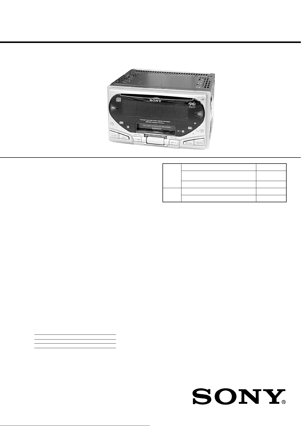
WX-4500X
SERVICE MANUAL
Ver 1.1 2002. 10
Dolby noise reduction manufactured under license from Dolby Laboratories Licensing Corporation.
“DOLBY” and the double-D symbol ; are trademarks of Dolby
Laboratories Licensing Corporation.
CD
Section
TC
Section
US Model
Model Name Using Similar Mechanism NEW
CD Drive Mechanism Type
Optical Pick-up Name RAF0143A
Model Name Using Similar Mechanism WX-C55
Tape Transport Mechanism Type MG-25E-136
MG-318RW/
A-153
AUDIO POWER SPECIFICATIONS
POWER OUTPUT AND TOTAL HARMONIC DISTORTION
23 watts per channel minimum continuous average power into
4 ohms, 4 channels driven from 20 Hz to 20 kHz with no more
than 5% total harmonic distortion.
CD player section
Signal-to-noise ratio 92 dB
Frequency response 10 – 20,000 Hz
Wow and flutter Below measurable limit
Laser Diode Properties
Material GaAlAs
Wavelength 780 nm
Emission Duration Continuous
Laser output power Less than 44.6 µW*
* This output is the value measured at a distance
of 200 mm from the objective lens surface on
the Optical Pick-up Block.
Cassette player section
Tape track 4-track 2-channel stereo
Wow and flutter 0.08 % (WRMS)
Frequency response 30 – 18,000 Hz
Signal-to-noise ratio
Cassette type Dolby B NR Dolby NR off
TYPE II, IV 67 dB 58 dB
TYPE I 64 dB 55 dB
SPECIFICATIONS
Tuner section
FM
Tuning range FM tuning interval:
50 kHz/200 kHz switchable
87.5 – 108.0 MHz
(at 50 kHz step)
87.5 – 107.9 MHz
(at 200 kHz step)
Antenna terminal External antenna connector
Intermediate frequency 10.7 MHz/450 kHz
Usable sensitivity 8 dBf
Selectivity 75 dB at 400 kHz
Signal-to-noise ratio 65 dB (stereo),
70 dB (mono)
Harmonic distortion at 1 kHz
0.7% (stereo),
0.4% (mono)
Separation 35 dB at 1 kHz
Frequency response 30 – 15,000 Hz
– Continued on next page –
9-873-326-02
2002J0400-1
© 2002. 10
CHANGER CONTROL AUDIO MASTER
Sony Corporation
e Vehicle Company
Published by Sony Engineering Corporation
1
Page 2

WX-4500X
AM
Tuning range AM tuning interval:
9 kHz/10 kHz switchable
531 - 1,602 kHz
(at 9 kHz step)
530 – 1,710 kHz
(at 10 kHz step)
Antenna terminal External antenna connector
Intermediate frequency 10.7 MHz/450 kHz
Sensitivity 30 µV
Power amplifier section
Outputs Speaker outputs
(sure seal connectors)
Speaker impedance 4 – 8 ohms
Maximum power output 50 W × 4 (at 4 ohms)
General
Outputs Audio output
Subwoofer outout (mono)
Power antenna relay
control lead
Power amplifier control
lead
Inputs Telephone ATT control lead
Illumination control lead
BUS control input
connector
BUS audio input connector
Remote controller input
connector
Antenna input connector
T one controls Bass ±10 dB at 62 Hz
Treble ±10 dB at 16 kHz
Loudness +8 dB at 100 Hz
+2 dB at 10 kHz
Power requirements 12 V DC car battery
(negative ground)
Dimensions Approx. 178 × 100 × 186 mm
(7 1/8 × 4 × 7 3/8 in.)
(w/h/d)
Mounting dimension Approx. 178 × 100 × 165 mm
(7 1/8 × 4 × 6 1/2 in.)
(w/h/d)
Mass Approx. 2.1 kg (4 lb. 10 oz.)
Supplied accessories Parts for installation and
connections (1 set)
SERVICE NOTE
CAUTION
Use of controls or adjustments or performance of procedures other than those specified herein may result in hazardous radiation exposure.
Notes on Chip Component Replacement
• Never reuse a disconnected chip component.
• Notice that the minus side of a tantalum capacitor may be dam-
aged by heat.
NOTES ON HANDLING THE OPTICAL PICK-UP BLOCK
OR BASE UNIT
The laser diode in the optical pick-up block may suffer electrostatic
breakdown because of the potential difference generated by the
charged electrostatic load, etc. on clothing and the human body.
During repair, pay attention to electrostatic breakdown and also use
the procedure in the printed matter which is included in the repair
parts.
The flexible board is easily damaged and should be handled with
care.
NOTES ON LASER DIODE EMISSION CHECK
The laser beam on this model is concentrated so as to be focused on
the disc reflective surface by the objective lens in the optical pickup block. Therefore, when checking the laser diode emission, observe from more than 30 cm away from the objective lens.
NOTES ON PICK-UP FLEXIBLE BOARD
The pick-up flexible board in this set is secured to the optical pickup with an adhesive tape. Once the tape is removed, an adhering
force becomes weak, and it cannot be reused.
Therefore, if the optical pick-up is replaced, replace also the pickup flexible board with a new one.
NOTE
This unit cannot be connected to a digital preamplifier
or an equalizer.
Design and specifications are subject to change without
notice.
SAFETY-RELATED COMPONENT WARNING!!
COMPONENTS IDENTIFIED BY MARK 0 OR DOTTED LINE
WITH MARK 0 ON THE SCHEMATIC DIAGRAMS AND IN
THE PARTS LIST ARE CRITICAL TO SAFE OPERATION.
REPLACE THESE COMPONENTS WITH SONY P ARTS WHOSE
PART NUMBERS APPEAR AS SHOWN IN THIS MANUAL OR
IN SUPPLEMENTS PUBLISHED BY SONY.
2
Page 3

TABLE OF CONTENTS
WX-4500X
1. GENERAL
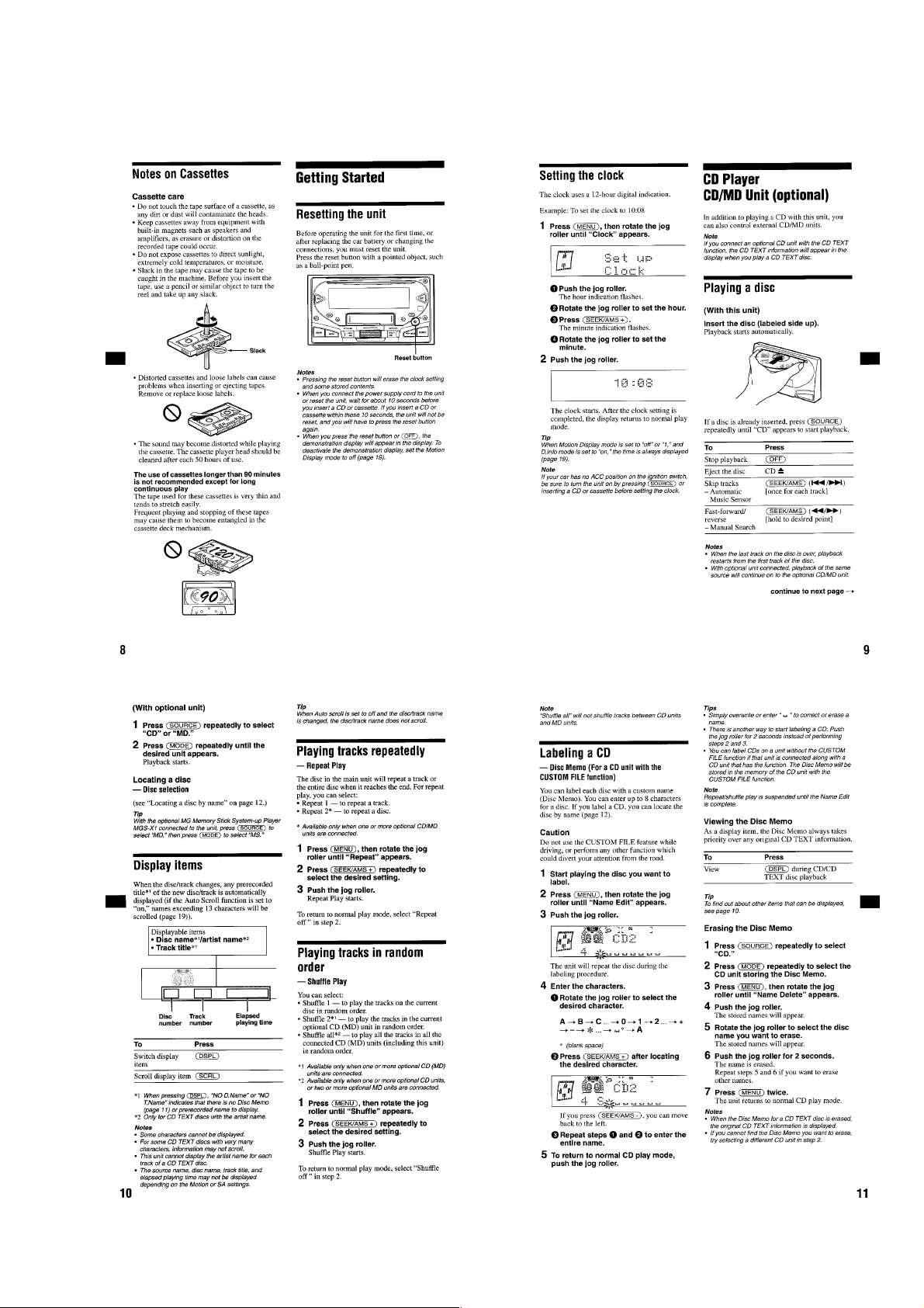
Location of Controls............................................................... 4
Getting Started........................................................................ 5
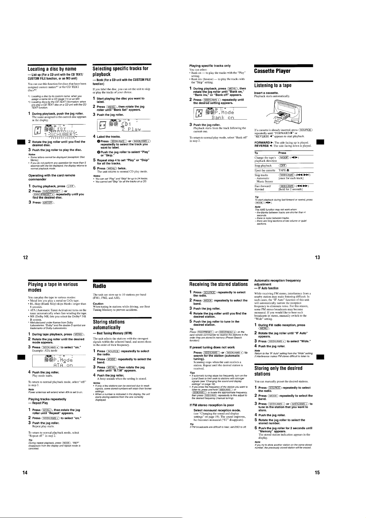
CD Player ............................................................................... 5
Cassette Player ....................................................................... 6
Radio ...................................................................................... 6
Other Functions ...................................................................... 7
Connections ............................................................................ 9
2. DISASSEMBLY
2-1. Front Panel Assy .............................................................. 11
2-2. CD Mechanism Block ...................................................... 12
2-3. CD Main Board ................................................................ 12
2-4. Tension Spring (FL) ......................................................... 13
2-5. Floating Block Assy ......................................................... 13
2-6. Roller Arm Assy ............................................................... 14
2-7. Optical Pick-up Assy........................................................ 14
2-8. Chassis (Top) Assy........................................................... 15
2-9. Main Board ...................................................................... 15
2-10. Heat Sink .......................................................................... 16
2-11. Tape Mechanism Block .................................................... 16
3. ASSEMBLY OF MECHANISM DECK
3-1. Housing ............................................................................ 17
3-2. Arm (Suction)................................................................... 17
3-3. Lever (LDG-A)/(LDG-B) ................................................ 18
3-4. Gear (Loading FT) ........................................................... 18
3-5. Guide (U) ......................................................................... 19
3-6. Main Motor Assy ............................................................. 19
5. ELECTRICAL ADJUSTMENTS
Tape Section ......................................................................... 20
6. DIAGRAMS
6-1. IC Pin Descriptions .......................................................... 22
6-2. Block Diagram –CD Section–.......................................... 26
6-3. Block Diagram –Tuner Section–...................................... 27
6-4. Block Diagram –Tape Section– ....................................... 28
6-5. Circuit Boards Location ................................................... 29
6-6. Printed Wiring Boards –CD Mechanism Section–........... 30
6-7. Schematic Diagram –CD Mechanism Section – .............. 31
6-8. Printed Wiring Board –Main Section–............................. 32
6-9. Schematic Diagram –Main Section (1/3)– ....................... 34
6-10. Schematic Diagram –Main Section (2/3)– ....................... 35
6-11. Schematic Diagram –Main Section (3/3)– ....................... 36
6-12. Printed Wiring Board –Jog Section– ................................ 37
6-13. Printed Wiring Board –Display Section– ......................... 38
6-14. Schematic Diagram –Display, Jog Section– .................... 40
7. EXPLODED VIEWS
7-1. Cover Section ................................................................... 46
7-2. Front Panel Section .......................................................... 47
7-3. Main Board Section ......................................................... 48
7-4. CD Mechanism Section (1) .............................................. 49
7-5. CD Mechanism Section (2) .............................................. 50
7-6. Tape Mechanism Section ................................................. 51
8. ELECTRICAL PARTS LIST ................................... 52
4. MECHANICAL ADJUSTMENTS.............................. 20
3
Page 4
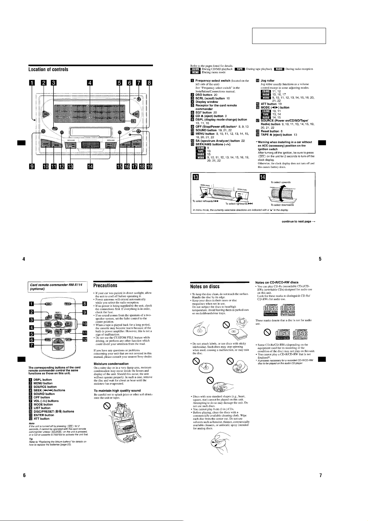
WX-4500X
SECTION 1
GENERAL
This section extracted from
instruction manual.
4
Page 5
WX-4500X
5
Page 6
WX-4500X
6
Page 7
WX-4500X
7
Page 8
WX-4500X
8
Page 9
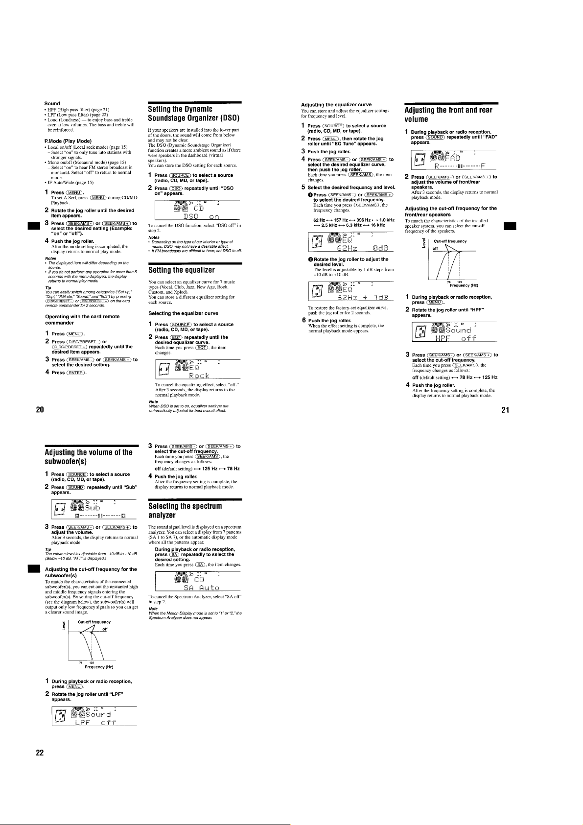
Connections
WX-4500X
99
Page 10
WX-4500X
10 10
Page 11
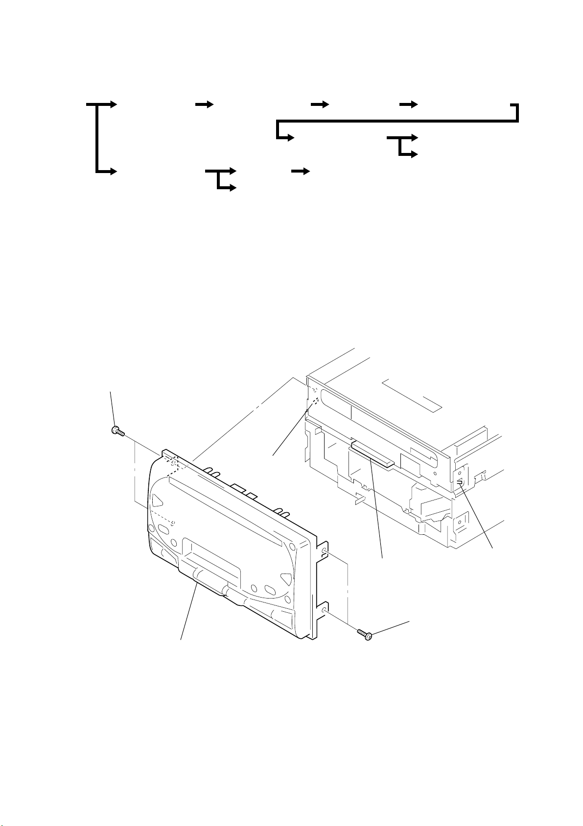
SECTION 2
w
DISASSEMBLY
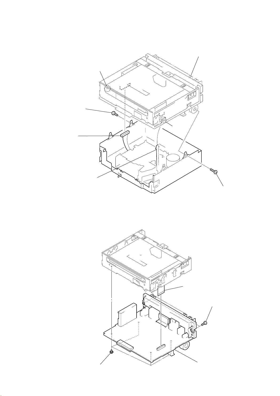
Note : This set can be disassemble according to the following sequence.
WX-4500X
Set Front Panel Assy CD Mechanism Block
Floating Block Assy Roller Arm Assy
Chassis (Top) Assy
Main Board Heat Sink
Tape Mechanism Block
Note : Follow the disassembly procedure in the numerical order given.
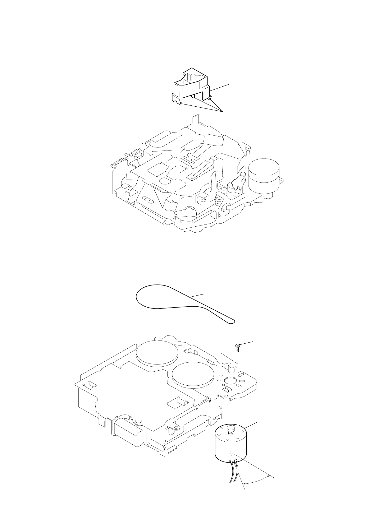
2-1. FRONT PANEL ASSY
1
PTT 2.6x6
CD Main Board Tension Spring (FL)
Optical Pick-up Assy
6
panel assy, front
4
claw
5
CN901
2
PTT 2.6x6
3
cla
11
Page 12
WX-4500X
2
)
2-2. CD MECHANISM BLOCK
4
CD mechanism block
3
PTT 2.6x6
6
PTT 2.6x6
7
bracket (MD
2-3. CD MAIN BOARD
6
CD MAIN board
1
PTT 2.6x6
4
M 2x3.0
3
CNJ103
5
CNJ101
2
CNJ102
2
PTT 2.6x6
5
M 2x3.0
12
claw
1
CNP10
Page 13
y
2-4. TENSION SPRING (FL)
1
spring (FL), tension
2
spring (FL), tension
WX-4500X
2-5. FLOATING BLOCK ASSY
5
spring (angle), tension
6
Fit lever in the
direction of the arrow.
7
shaft
8
shaft
9
4
spring (SPM), tension
0
floating block ass
shaft
3
lever (LE.L)
2
1
washer (M)
13
Page 14
WX-4500X
2-6. ROLLER ARM ASSY
3
Fit lever in the
direction of the arrow.
5
shaft
2
spring (roller)
6
arm assy, roller
1
spring (roller)
4
shaft
2-7. OPTICAL PICK-UP ASSY
2
shaft (sled guide)
5
rack (feed)
1
gear (woam wheel)
4
PTP 1.7x4
3
cover (P)
6
pick-up assy, optical
14
Page 15
1
PTT 2.6x10
2
PTT 2.6x6, ground point
3
MAIN board
4
CN450
6
2-8. CHASSIS (TOP) ASSY
2
PTT 2.6x6
4
connector
projection
projection
5
chassis (TOP) assy
WX-4500X
2-9. MAIN BOARD
3
CN400
1
PTT 2.6x
15
Page 16
WX-4500X
2-10. HEAT SINK
6
heat sink
5
4
BTP 2.6x8
PTT 2.6x10
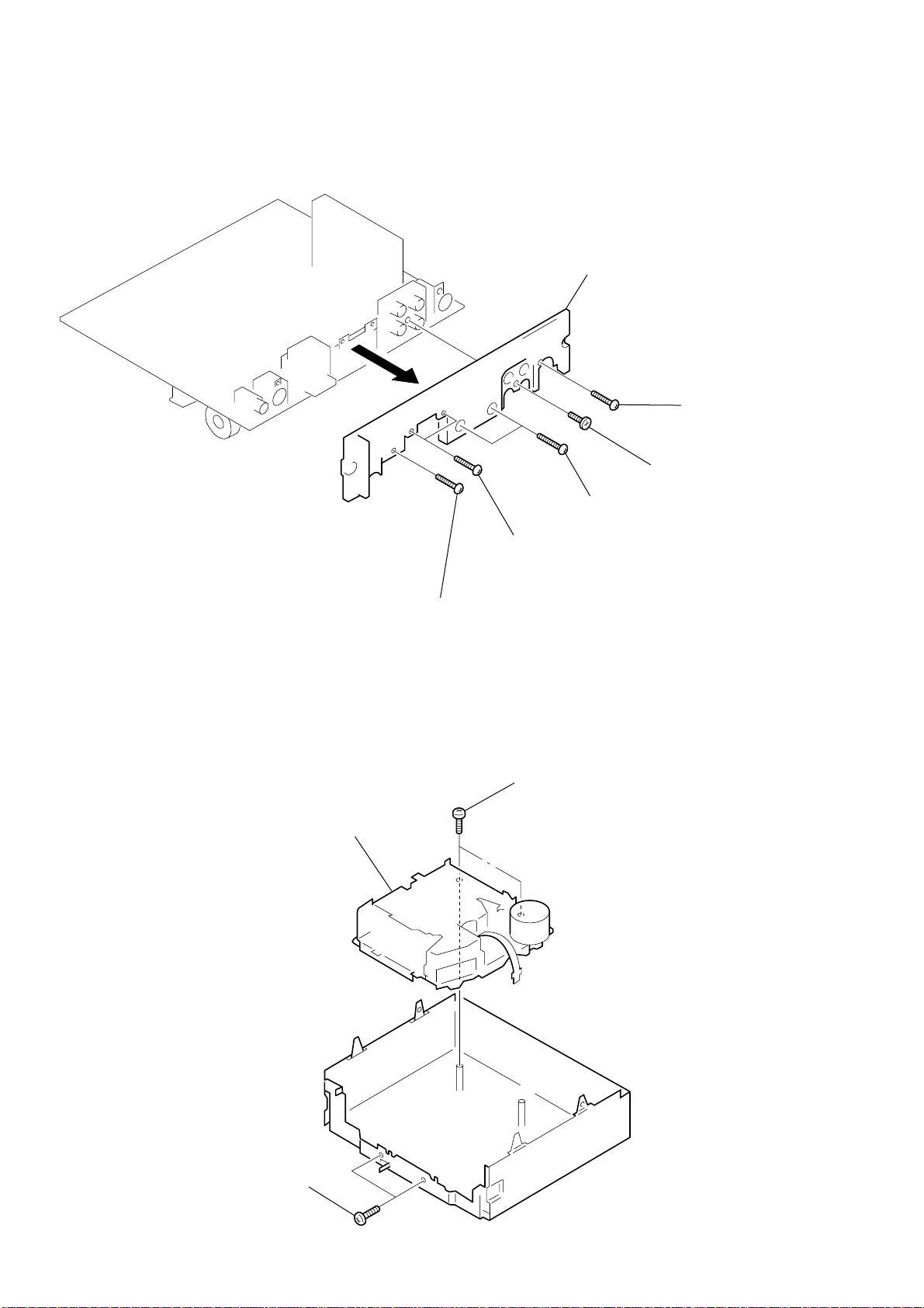
2-11. TAPE MECHANISM BLOCK
3
tape mechaniam block
1
PTT 2.6x10
2
PTT 2.6x10
2
PTT 2.6x5
3
PTT 2.6x10
16
1
PTT 2.6x5
Page 17
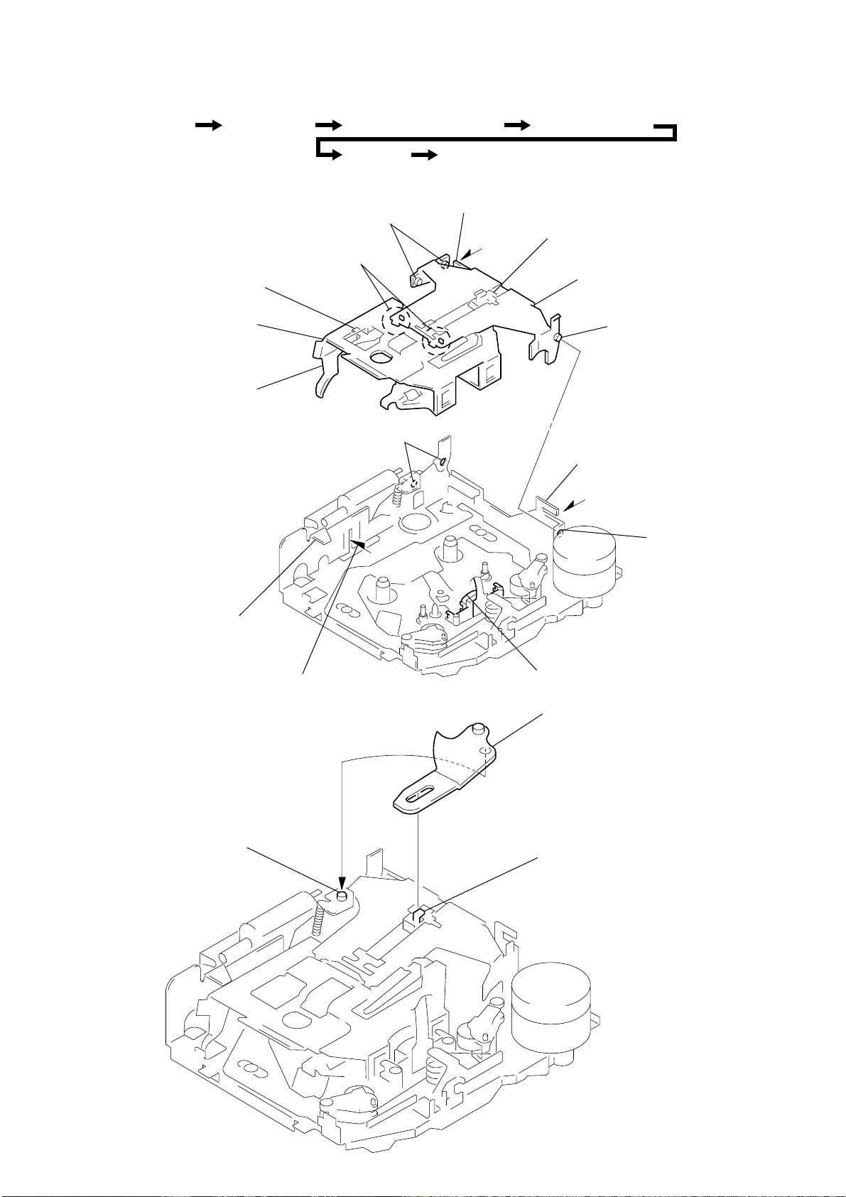
w
SECTION 3
ASSEMBLY OF MECHANISM DECK
Note : This set can be assemble according to the following sequence.
Head, Housing Arm (Suction)
Note : Follow the assembly procedure in the numerical order given.
3-1. HOUSING
4
3
Put the housing
under
2
Fit claw on B part.
A
part.
housing
5
Install the hanger onto
two claws of the housing.
Lever (LDG-A) / (LDG-B) Gear (Loading FT)
Guide (U) Main Motor Assy
Fit projection on C part.
C
part
7
Holder the hanger by bending the claw.
1
Install the catcher to the hanger.
hanger
6
Fit projection on D part.
WX-4500X
3-2. ARM (SUCTION)
projection
A
part
B
part
8
Hold the hanger by
bending the claw.
D
part
head
2
Move the arm (suction) in the arro
Direction and fit on projection.
1
Fit the arm (suction) on the shaft.
17
Page 18
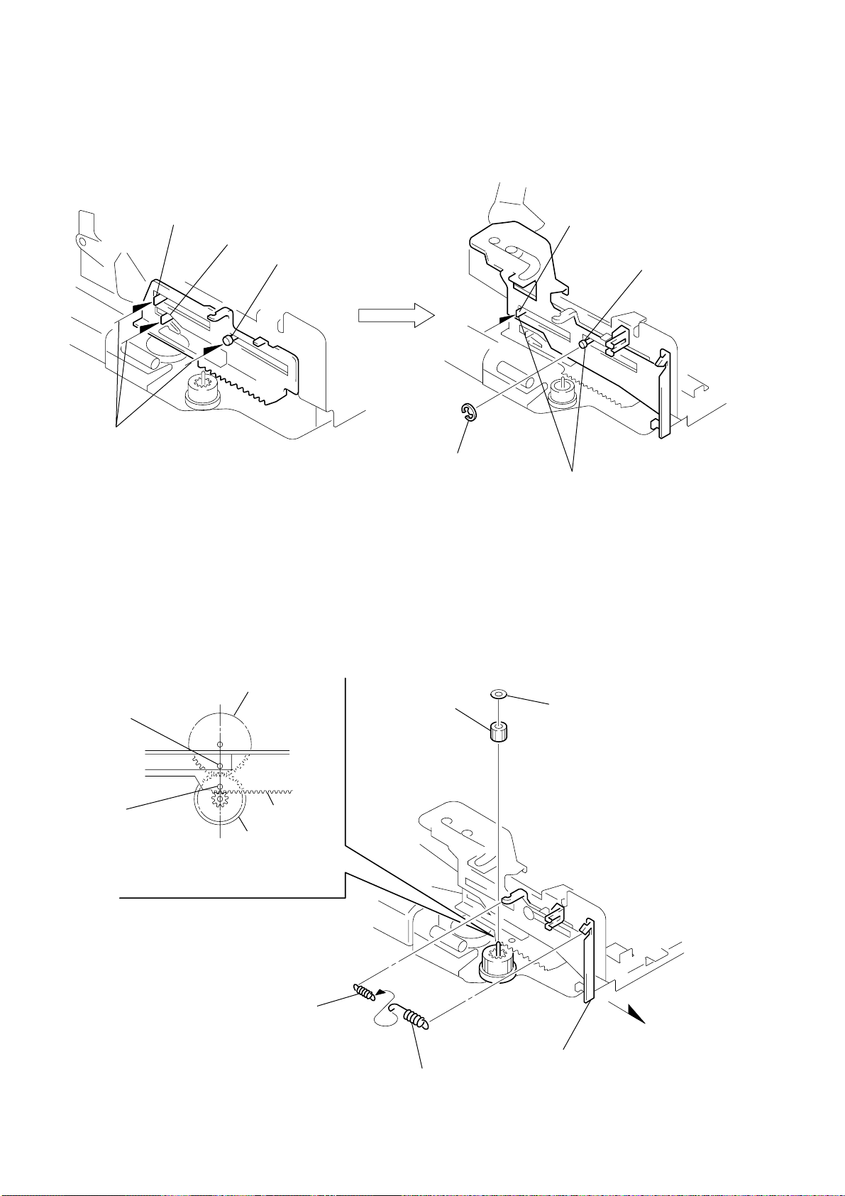
WX-4500X
3-3. LEVER (LDG-A) / (LDG-B)
A
shaft
shaft
1
Fit the lever (LDG-A) on
shafts
A
to C and install it.
B
shaft
C
3
type-E stop ring 2.0
shaft
A
2
Fit the lever (LDG-B) on
shafts
A
and B and install it.
shaft
B
3-4. GEAR (LOADING FT)
hole
hole
5
Align hole in the gear (LDG-D)
with hole the lever (LDG-A).
2
gear (LDG-D)
lever (LDG-A)
gear (LDG-FB)
tension spring (LD-2)
6
gear (loading FT)
1
7
polyethylene washer
18
tension spring (LD-1)
3
4
Move the lever (LDG-B)
in the arrow direction.
Page 19
3-5. GUIDE (U)
)
1
2
claws
WX-4500X
guide (C)
3-6. MAIN MOTOR ASSY
3
belt (25)
2
precision screws P 2x2
1
main motor assy
(CAPSTAN/REEL) (M904
30
°
19
Page 20

WX-4500X
SECTION 4
MECHANICAL ADJUSTMENTS
SECTION 5
ELECTRICAL ADJUSTMENTS
PRECAUTION
1. Wipe the following components with an absorbent cotton cloth
moistened with alcohol before adjustment :
PB head Pinch roller
Idler Rubber belt
Capstan
2. Demagnetize the PB head using a head demagnetizer.
3. Be careful not to use a magnetized screwdriver.
4. After the adjustment is completed, lock the adjustment parts
using screws.
5. Unless otherwise specified, make adjustments at the specified
voltage (14.4 V).
Torque Measurement
Mode Torque Meter Meter Reading
2.95 – 6.37 mN • m
FWD (30 – 65 g • cm)
CQ-102C
FWD
Back Tension
REV (30 – 65 g • cm)
CQ-102RC
REV
Back Tension
FF, REW CQ-201B (60 – 200 g • cm)
(0.42 – 0.90 oz • inch)
0.05 – 0.44 mN • m
(0.5 – 4.5 g • cm)
(0.01 – 0.06 oz • inch)
2.95 – 6.37 mN • m
(0.42 – 0.90 oz • inch)
0.05 – 0.44 mN • m
(0.5 – 4.5 g • cm)
(0.01 – 0.06 oz • inch)
5.88 – 19.61 mN • m
(0.83 – 2.78 oz • inch)
• Adjustments of the tuner and CD sections have auto adjustments
in this set.
TAPE SECTION
Test tape
Type Signal Use
WS-48A 3 kHz, 0 dB Tape speed adjustment
P-4-D400 400 Hz, 0 dB Dolby level adjustment
Tape Speed Adjustment
Mode : FWD play
test tape
WS-48A
(3 kHz, 0 dB)
Procedure:
1. Playback the test tape in the FWD play mode.
2. V erify that the reading on the digital frequency counter is in the
range between 3,010 and 3,300 Hz at the top of tape.
3. If the specified value is not met, adjust the variable resistor on
the capstan motor so that the reading is 3,000 Hz at the FWD
top of tape.
Adjustment Location :
0 dB = 0.775 V
set
SP OUT
frequency counter
4
Ω
Tape Tension Measurement
Mode Tension Meter Meter Reading
FWD CQ-403A more than 90 g
REV CQ-403R (more than 3.17 oz)
-Tape Mechanism Block upper side-
Tape Speed Adjustment
20
Page 21

t
DOLBY Level Adjustment
Setting :
Light down mark ;
(DOLBY OFF)
test tape
P-4-D400
(400 Hz, 0 dB)
set
main board
TP-L
TP-R
level meter
Procedure :
1. Set the FWD play mode.
2. Push the MENU button and rotate the jog roller to display “NR”.
Then press “ — ” on the SEEK/AMS button to select “NR off”.
(Dolby off)
3. Adjust RV400 for L-ch and RV401 for R-ch so that the level
meter reads –6 ±0.5 dB (0.37 to 0.41 V).
WX-4500X
Adjustment Location :
Dolby level adjustment
(L-CH)
-MAIN BOARD(SIDE A)
Dolby level adjustmen
(R-CH)
-MAIN BOARD(SIDE B)
TP-R TP-L
Dolby level adjustment
21
Page 22

WX-4500X
SECTION 6
DIAGRAMS
6-1. IC PIN DESCRIPTIONS
• IC103 µPD780058GC-259-8BT (CD MECHANISM CONTROLLER)
Pin No. Pin Name I/O Pin Description
1 RST O Reset signal output to the MN6627481RPMF A (IC101) “L” : Reset
2, 3 — O Not used in this set (open)
4 AVSS — Ground pin (for A/D converter)
5 — O Not used in this set (open)
6 J/E, CE I Destination initial setting pin Fixed at “H” in this set
7 A VREF1 I Reference voltage (+5 V) input (for D/A converter)
8 SUBQ I Sub code Q data input from the MN6627481RPMFA (IC101)
9 — O Not used in this set (open)
10 SQCK O Clock signal output for sub code Q data write to the MN6627481RPMFA (IC101)
11 STAT I Internal status signal input from the MN6627481RPMFA (IC101)
12 FL-M- > F O Data write signal to external flash memory Not used in this set (open)
13 MCLK/FL-CLK O Clock signal output for command data from the MN6627481RPMFA (IC101)
14, 15 — O Not used in this set (open)
16 BUS SI I Serial data input from SONY bus interface (IC750)
17 BUS SO O Serial data output to SONY bus interface (IC750)
Serial clock signal input/output for bus interface to the master controller (IC700) and
18 BUS CLK I/O
19 — I
20 TLOCK I Tracking servo pull-in signal input from the MN6627481RPMFA (IC101) “L” : Active
21 FLOCK I Focus servo pull-in signal input from the MN6627481RPMFA (IC101) “L” : Active
22 SENCE I Internal status (SENSE) input from the MN6627481RPMFA (IC101)
23 — I
24 — O Through pin of bus serial data out Connect to the BUS SO (pin qj)
25, 26 — I Through pin of bus serial data in Connect to the BUS SI (pin qh)
27 MLD O Command road signal output from the MN6627481RPMFA (IC101)
28 MDATA O Command data signal output from the MN6627481RPMFA (IC101)
29 LINK OFF O
30 A MUTE O Audio line mute control signal output “H” : mute on
31 MECHA ON O Power on/off control signal output of CD mechanism deck block “H” : Power on
32 — I Through pin of power supply Connect to the VDD (pins yk, uf)
33 VSS — Ground pin
34 — I Through pin of battery down voltage detection signal
35 CD ON O Power on/off control signal output of CD mechanism deck block
36 – 38 — O Not used in this set (open)
39 — I Through pin of bus on/off control signal
40 — O Not used in this set (open)
41 — I Test signal input of auto adjustment
42 SER OK O Effect discrimination out of auto adjustment “H” : OK
43 SER NG O Effect discrimination out of auto adjustment “H” : NG
44 – 51 — O Not used in this set (open)
52 TEXT I
53 SERCHK O Not used in this set (open)
54 P TEST O Not used in this set (open)
55 LIMSW I
56, 57 — O Not used in this set (open)
the display controller (IC900), or serial clock signal output to the SONY bus
interface (IC750)
Through pin of serial clock signal for the bus interface
Connect to the BUS CLK (pin qk)
Through pin of serial clock signal for the bus interface
Connect to the BUS CLK (pin qk)
Link on/off control signal output for SONY bus interface
“L” : Link off, “H” : Link on Not used in this set
Initial setting input used to with/without the CD text decording function
“L” : without, “H” : with
CD sled limit in detection switch input
“L” signal is input when the optical pick-up comes on the innermost perimeter
22
Page 23

WX-4500X
Pin No. Pin Name I/O Pin Description
58 SW3 I
59 SW4 I
60 SYS RESET I
61 — O Not used in this set (open)
62 BUS ON I BUS on/off control signal input from the master controller (IC700) “L” : Bus on
63 SW2 I
64 B/U CHECK I
65 BLKCK I Clock signal input for sub code interrupt from the MN6627481RPMFA (IC101)
66 — O Not used in this set (open)
67 VSS0 — Ground pin
68 VDD — Power supply pin (+5 V)
69 X2 — Main system clock connect pin (5 MHz)
70 X1 — Main system clock connect pin (5 MHz)
71 VPP — Fixed at “L” in this set
72 ——Sub System clock connect pin Not used in this set (open)
73 XT1 — Sub System clock connect pin Not used in this set (Fixed at “H”)
74 VDD — Power supply pin (+5 V)
75 A VREF0 I Reference voltage input (for A/D converter) Fixed at “L” in this set
76 ROUT O
77 FOUT O
78, 79 ——Not used in this set (open)
80 GCTL O FE, TE gain control signal output
CD loading detection switch input
“L” signal is input during CD disc loading and ejecting operations
CD disc detection switch input
“L” signal is input when CD disc catching is completed
System reset signal input from the master controller (IC700) and the reset signal
oscillator (IC701) “L” : Reset
“L” signal is input for several hundreds of microseconds after the power is turned on,
the signal then turns “H”.
CD disc detection switch input
“L” signal is input when a disc is present at the CD disc inlet
Down voltage detection input from the SONY bus interface (IC750) and the battery
detection circuit “L” signal is input when the voltage is reduced
CD loading motor (M903) control signal (direction of eject) output to the
BA5984FP (IC201) of CD mechanism deck block “H” : Active
*1
CD loading motor (M903) control signal (direction of loading) output to the
BA5984FP (IC201) of CD mechanism deck block “H” : Active
*1
*1 CD loading motor (M903) control
Operation
Pin
STOP LOADING EJECT BRAKE
FOUT (Pin uj) “L”“H”“L”“H”
ROUT (Pin uh) “L”“L”“H”“H”
23
Page 24

WX-4500X
• IC700 MB90574CPMT-G-356-BNDDE1 (MAIN SYSTEM CONTROL)
Pin No. Pin Name I/O Pin Description
1 TU ON O Tuner on signal output
2 DOLON I/O
3 – 6 N. C. O O Not used in this set (open)
7 BUS ON O Bus on control signal output
8 VCC — Power supply pin (+5 V)
9 FLASH WR I Flash write mode detection signal input “L” : Flash write mode
10 EEDATA I/O EEPROM data signal input/output
11 EECLK O EEPROM clock signal output
12 RXD I Flash write data signal input
13 TXD O Flash write data signal output
14 N. C. O O Not used in this set (open)
15 BEEP O BEEP signal output
16 DPBOOT O Display microcomputer write control signal output
17 – 19 N. C. O O Not used in this set (open)
20 UNI SI I SONY bus data input
21 UNI SO O SONY bus data output
22 UNI CLK O SONY bus clock output
23 N. C. O O Not used in this set (open)
24 SIRCS I Remote control data signal input
25 – 28 POS0 – 3 I Position signal detection input
29 REEL1 I Reel stand rotation detection signal input
30 LM EJ O Tape mechanism loading motor control signal output (eject direction)
31 LM LOD O Tape mechanism loading motor control signal output (loading direction)
32 TP ON O Tape power control signal output
33 VSS — Ground pin
34 C — Capacitance pin of power stabilized
35 AD ON O Power control signal output of A/D conversion
36 N. C. O O Not used in this set (open)
37 CM-ON O Capstan motor control signal output
38 DVCC — D/A converter VREF input
39 DVSS — D/A converter ground pin
40, 41 N. C. O O Not used in this set (open)
42 AVCC — Analog power supply pin
43 A VRH — A/D converter VREF+ input
44 A VRL — A/D converter VREF– input
45 AVSS — Analog ground pin
46 KEY IN0 I Key 0 signal input
47 KEY IN1 I Key 1 signal input
48 DESTSEL0 I Destination initial setting pin (Fixed at “H” in this set)
49 RC IN0 I Rotary commander signal input
50 QUALITY I Tuner noise detection signal input Not used in this set (open)
51 FM AGC I FM AGC detection signal input
52 MPT I Tuner multi pass signal input Not used in this set (open)
53 VSM I S meter voltage signal input
54 VCC — Power supply pin (+5 V)
55, 56 N. C. O — Not used in this set (open)
57 E VOL MUTE O Electronic volume mute signal output “L” : mute on
58 AMP MUTE O Amplifier mute signal output
59 MUTE O System mute control signal output
60 AMP ON O Amplifier on signal output “L” : off/ “H” : on
61 SA LAT O Serial data lutch pulse output for spectrum analyzer
Dolby control signal output (“H” : dolby on)/dolby function corresponding
detection signal input (“L” : dolby function corresponding)
24
Page 25

Pin No. Pin Name I/O Pin Description
62 FL ON I FL ON control signal input
63 VSS — Ground pin
64 RE IN1 I Rotary encoder signal input
65 FSW IN I Frequency signal input for D/D converter oscillation
66 RE IN0 I Rotary encoder signal input
67 – 69 N. C. O O Not used in this set (open)
70 II DATA O Data signal output for tuner volume communication
71 II CLK O Clock signal output for tuner volume communication
72 RC IN1 I Rotary commander signal input
73 X1A — Low speed oscillation input (32.768 kHz)
74 X0A — Low speed oscillation input (32.768 kHz)
75 W UP O Wake up signal output
76 KEYACK I Key acknowledge detection signal input
77 BU CHK I Back up power detection signal input
78 DAVN I RDS data block synchronization detection signal input
79 TEL ATT I TEL mute detection signal input
80 TEST IN I Test mode setting detection signal input
81 ACC IN I ACC power detection signal input “L” : ACC on
82 FSW SFT O D/D converter control signal output
83 SYS RST O System reset signal output
84 RAM RST I RAM reset detection signal input
85 NS MASK O Noise mask output Not used in this set (open)
86 HTMX I Hardware standby signal input
87 MODE2 I Input for operation mode (Connect to VSS)
88 MODE1 I Input for operation mode (Connect to VSS)
89 MODE0 I Input for operation mode (Connect to VSS)
90 RST I Microcomputer reset signal input
91 VSS — Ground pin
92 X0 — High speed oscillation input (3.58 MHz)
93 X1 — High speed oscillation input (3.58 MHz)
94 VCC — Power supply pin (+5 V)
95 DSTSEL1 I Destination initial setting pin
96, 97 N. C. O O Not used in this set (open)
98 DIM ON O Dimer control signal output
99 ILL ON O Illumination power control signal output
100 ILL IN I Illumination line detection signal input
101 – 103 N. C. O O Not used in this set (open)
104 POWER ON O System power control signal output
105 – 110 N. C. O O Not used in this set (open)
111 PLAY/AMS O AMS music interval detection function control signal output
112 F/R O FWR/REV control signal output “H” : FWD/ “L” : REV
113 MTL I/O
114 – 116 N. C. O O Not used in this set (open)
117 AMS IN I
118 TAPE MUTE O
119 VSS — Ground pin
120 N. C. O O Not used in this set (open)
Metal control signal output (“H” : metal on)/Metal function corresponding detection
signal input
AMS music interval detection signal input
“L” : Audio signal detection, “H” : Audio signal no detection
During FF/REW period, audio signal select control signal output
When the FF/REW mode is selected with ATA ON : “H”
WX-4500X
25 25
Page 26

WX-4500X
6-2. BLOCK DIAGRAM — CD SECTION —
DETECTOR
&
I/V AMP
OPTICAL
PICK-UP
BLOCK
LASER DIODE
NA
NB
F
E
AUTOMATIC
LD
POWER
CONTROL
Q101
PD
A
32
B
30
PDF
28
PDE
27
LD
2
LPD AMP
PD
1
I-V
AMP
RF AMP
RFO RFI
5
ERROR AMP
TRACKING
ERROR AMP
6 8
FOCUS
RF AMP,
FOCUS/TRACKING ERROR AMP
RF
DET
RF AMP
IC102
BDO
DET
AGC
OFER
DET
ENVELOPE
ARF
ENV
NRFDET
OFTR
BDO
FEO
TEO
TEBPF
VDET
TBAL
FBAL
LDON
DIGITAL SIGNAL PROCESSOR,
DIGITAL SIGNAL SERVO,
CLV SERVO,
D/A CONVERTER,CD-TEXT
IC101
ARF
44
53
10
15
14
38
36
DSLB
RFDET
OFT
DSL.
PLL VCO
SERVO TIMING
GENERATOR
68
EFM/SUBCODE
DEMODULATOR,
CD-TEXT
BUFFER
CIRC ERROR
CORRECTION,
16K S-RAM
SUBCODE
BUFFER
TIMING
GENERATOR
SOFT
MUTING,
ATTENUATOR
DIGITAL
DEEMPHASIS
DIGITAL
FILTER
BLKCK
1BIT D/A
CONVERTER,
PWM LOGIC
SUBQ
15 8
SQCK
14 10
13 65
16M
OUTL
OUTR
SUBQ
SQCK
BLKCK
X2
58
59
73
75
35 31
CD-ON
X101
16.93MHz
R-CH
MECHA ON
A-MUTE
2
TUNER
SECTION
CD L
(Page 27)
CD ON
MECHA ON
30
A-MUTE
3
6
SECTION
(Page 28)
TUNER
SECTION
TAPE
(Page 27)
BDO
12
23
20
B.P.F
19
18
26
25
24
39
RFENV
34
FE
32
TE
33
VDET
35
TBAL
31
FBAL
30
LDON
40
A/O
CONVERTER
INPUT
PORT
SERVO CPU
SERVO TIMING
GENERATOR
MICRO
COMPUTER
INTERFACE
SENSE
10 22
FLOCK
11 21
TLOCK
12
MDATA
8
MCLK
7
MLD
9
STAT
17
20
28
13
27
11
SENSE
FLOCK
TLOCK
MDATA
MCLK
MLD
STAT
CD MECHANISM
CONTROLLER
IC103
BUS CLK
BUS SO
BUS SI
BUS ON
B/U CHECK
SYS RESET
18
17
16
62
64
60
BUS CLK
BUS SO
BUS SI
BUS ON
BUS CHECK
SYS RST
7
TAPE
SECTION
(Page 28)
2-AXIS
DEVICE
(FOCUS)
(TRACKING)
F+
F–
T+
T–
• Signal path
: CD
• R-ch is omitted due to same as L-ch.
M902
SLED
M901
SPINDLE
M903
LOADING
18
F+
17
F–
18
T+
15
T–
16
+
M
–
+
M
–
+
M
–
SLED+
12
SLED–
11
SPDL+
14
SPDL–
13
VOL+
10
VOL–
9
FOCUS COIL
DRIVE
TRACKING COIL
DRIVE
SLED MOTOR
DRIVE
SPINDLE MOTOR
DRIVE
LOADING MOTOR
DRIVE
FOCUS/TRACKING COIL DRIVE,
SLED/SPINDLE/LOADING
MOTOR DRIVE
IC201
FIN–
TIN–
SLIN–
SPIN–
FIN
RIN
23
26
6
3
28
1
FOD
28
TRD
27
KICK
26
TVD
22
TRV
21
ECM
24
ECS
25
CLV
SERVO
SW2
(DISC DETECT)
SW3
(LOADING DETECT)
SW4
(CHUCKING DETECT)
SW5
(LIMIT)
RST
X301
5MHz
1
RST
70
X1
X2
69
FOUT
77
ROUT
76
63
SW2
SW3
58
59
SW4
55
LIMSW
2626
Page 27

6-3. BLOCK DIAGRAM — TUNER SECTION —
J1
(ANTENNA)
CD
SECTION
(Page 26)
2
1
2
TAPE
SECTION
(Page 28)
CD L
ANT-AM
ANT-FM
TU1
TUNER UNIT
1
3
AM DET
S-METER
FM AGC
MPX
SDA
SCL
SDA
SCL
TAPE L
8
10
12
13
14
4
17
18
1
LPF
IC451
4
44
40
9
12
CDC L
TAPE L
CD L
AM
MPXI
14
MP IN
ELECTRONIC VOLUME
IC300
ADSO(L-CH)
IC100
X700
32.768kHz
WX-4500X
CN300
-1
L
BUS AUDIO IN
-2
CN900
2
1
10
9
3
4
11
12
13
7
R
-3
L
SUB WOOFER OUT(MONO)
-4
R
FL+
FL–
RL+
RL–
FR+
FR–
RR+
RR–
TEST
ACC
SA OUT
23
21
SA CLK
SW
CD
59
60
58
15
80
81
24
FL
28
RL
27
(Page 26)
TAPE
SECTION
(Page 28)
S MUTE
57
E-VOL MUTE
AMP MUTE
BAL/
FAD
3
A-MUTE
MUTE
AMP ON
BEEP
TEST IN
ACC IN
SECTION
13 3338
53
51
10
11
73
74
VOL TONE
VSM
FM AGC
EE DATA
EE CLK
X1A
XOA
SDA
SCL
19
207117
70
II CLK
II DATA
MAIN
SYSTEM CONTROL
IC700(1/2)
MUTE DRIVE
Q300,301
5
SA AUDIO
SA CLK
RESET
4
SECTION
(Page 28)
ACC CHECK
Q903
TAPE
MUTE
MUTE
MUTE
Q303
Q303
Q303
MUTE
Q302
11
15
22
POWER AMP
IC170
OUT1+
IN1
IN3
MUTE
STBY
4
OUT1–
OUT3+
OUT3–
AC GND
16
R-CH
9
7
17
19
R-CH
• Signal path
: FM
: AM
: CD
: TAPE(PB)
• R-ch is omitted due to same as L-ch.
ILL IN
100
XO
X451
3.58MHz
1
COM8V TU5VAUDIO 10V BATT
+8V REG
4 2
IC301
92
TEL ATT
79
XI
93
BATT
TU ON
+5V REG
Q1
TU8.5V
POWER ON
1
104
1
REG
4 2
IC1
ANT/AMP
REMOTE SW
Q902
BATT
27 27
ILLUM CHECK
ANT REMOTE
SW
Q900(1/2)
AMP REMOTE
SW
Q900(2/2)
Q904
TEL ATT
Q906
BATT
F901
15
ILL
14
ATT
5
ANT REM
6
AMP REM
16
BATT
Page 28

WX-4500X
6-4. BLOCK DIAGRAM — TAPE SECTION —
HP901
PLAYBACK HEAD
FWD
REV
(CAPSTAN/REEL)
L
R
L
R
M904
+8.5V
MECHA ON
6
CD ON
R-CH
R-CH
M
37
39
C-MOTOR
Q653,654
TAPE +8.5V
Q650,651
CD
SECTION
(Page 26)
CD8V
Q450,451
• Signal path
: TAPE
• R-ch is omitted due to same as L-ch.
TAPE EQ/DOLBY/METAL/AMS
RV400
DOLBY LEVEL
(L-CH)
DRIVE
REG
+5V REG
CD5V
IC400
EQ
24
BATT
BATT
R-CH
DOLBY
AUTO
MUSIC
SENSOR
(LOADING)
J900
(REMOTE IN)
BU5V
NR
MECHANISM
M905
FWD/REV
MTL/NORMAL
NR ON
L OUT
MUTE/TAPE
AMS OUT
AMS/PLAY
TAPE
BLOCK
M
KEY
RESET
IC701
TUNER
SECTION
(Page 27)
19
18
16
7
17
14
20
LM
LM–
BU5V
12
5
TAPE L
(Page 27)
S700
(FREQUENCY SELECT)
FM 200k
AM 10k
FM 50k
AM 9k
+
REMOTE CONTROL
7
9
RECEIVER
PH960
KEY ACK SW
Q905
RESET
SW960
(RESET)
RESET
LOADING
MOTOR DRIVE
IC650
EN960
RAM
IC702
1
TUNER
SECTION
4
3
BU5V
MAIN SYSTEM CONTROL
112
F/R
113
MTL
2
DOL ON
118
TAPE MUTE
117
AMS IN
111
AMS ON
DST SEL1
95
POS0
25
POS1
26
POS2
27
28
POS3
29
REEL1
30
LM EJ
31
LM LOD
37
CM ON
SIRCS
24
32
TP ON
KEY ACK
76
35
AD ON
72
RC IN1
49
RC IN0
46
KEY IN0
66
RE IN0
RE IN1
64
8412
RAM RST
RST
90
HTMX
86
RXD
12
IC700(2/2)
UNI SI
UNI SO
BUS ON
UNI CLK
BU CHK
SYS RST
DP BOOT
SA LAT
DIM ON
ILL ON
W UP
FSW SFT
F SW IN
FL ON
CD SECTION
7
BUS CLK
BUS SI
BUS SO
BUS ON
20
21
7
22
77
83
16
61
98
99
75
82
65
62
(Page 26)
BUS CHECK
SYS RST
AUDIO 10V
AUDIO 10V
2
RESET
D/D CONV
ON/OFF SW
FREQ OSC
ON/OFF SW
Q801
FL ON/OFF
IC801,Q803
IC901
Q800
SW
DIMMER
ON/OFF SW
Q907
ILLUM
ON/OFF SW
Q908
BUS CONTROL
IC750
8
9
12
11
10
13
811
57
27
34
82
38
51
97
98
101
62
16
20
21
22
33
28
BUS ON
CONT
BATT
CHECK
RESET
DISPLAY SYSTEM CONTROL
IC900
LINK OFFRES
BOOT
SA LAT
BU IN
NMI
BUS ON
FL ON
UNI SO
UNI SI
UNI CK
FL SI
D903,905
908,911
D902,904,906
POWER CONTROL
CTL1
CTL2
CTL3
DTC4
DTC3
SA DATA
IC800
BATT
DATA
CLK
SA CLK
ILL ON
XTAL
EXTAL
FL LAT
FL BK
FL SCK
FL SO
OUT1RT
OUT2
OUT3
OUT4
6
1
4
3
2
50
1
112
52
85
86
75
74
64
60
BATT
46
44
40
39
FL ON/OFF
SW
Q810
18.432MHz
BATT
BUS ON/OFF
SW
Q750
X901
WAKE-UP
Q807
BATT
BACK-UP
+5V REG
Q804
BATT
OVER VOLTAGE
CHECK
Q751
SA CLK
SA AUDIO
BU5V
SW
CD+8V REG
Q809
AMP
IC803,Q810
Q812-814
ON/OFF SW
POWER
CONTROL
Q805,806
+10V REG
Q808
4
ILLUM
Q901
CD8V
TUNER
SECTION
(Page 27)
BU5V
AUDIO 10V
T800
CN750
(BUS CONTROL IN)
8
6
5
4
7
BATT
VDD
11
LAT
9
BK
10
8
CLK
SI
7
12
VH
F2 F2 F1 F1
16
3
2
1
17
FL700
1
2
2828
Page 29

WX-4500X
d
6-5. CIRCUIT BOARDS LOCATION
SW board
JOG board
DISPLAY board
CD MAIN board
MOTOR boar
MAIN board
THIS NOTE IS COMMON FOR PRINTED WIRING BOARDS
AND SCHEMATIC DIAGRAMS.
(In addition to this, the necessary note is
printed in each block.)
Note on Printed Wiring Boards:
• X : parts extracted from the component side.
• Y : parts extracted from the conductor side.
a
•
•
• : Pattern from the side which enables seeing.
Caution:
Pattern face side: Parts on the pattern face side seen from the
(Side B) pattern face are indicated.
Parts face side: Parts on the parts face side seen from the
(Side A) parts face are indicated.
Note on Schematic Diagram:
• All capacitors are in µF unless otherwise noted. pF: µµF
• All resistors are in Ω and 1/
• % : indicates tolerance.
•
• C : panel designation.
Note: The components identified by mark 0 or dotted line
• A : B+ Line.
• Power voltage is dc 14.4V and fed with regulated dc power
• Voltage and waveforms are dc with respect to ground
• Voltages are taken with a VOM (Input impedance 10 MΩ).
• Waveforms are taken with a oscilloscope.
• Circled numbers refer to waveforms.
• Signal path.
: Through hole.
f
: internal component.
(The other layer’s patterns are not indicated.)
50 WV or less are not indicated except for electrolytics
and tantalums.
specified.
f
: internal component.
with mark 0 are critical for safety.
Replace only with part number specified.
supply from ACC and BATT cords.
under no-signal conditions.
Voltage variations may be noted due to normal produc-
tion tolerances.
Voltage variations may be noted due to normal production tolerances.
F : FM
f : AM
E : TAPE
J : CD
4
W or less unless otherwise
• Waveforms
— CD MECHANISM SECTION —
(MODE : CD PLAY)
1
1.2Vp-p
IC102 8 (ARF)
2
0V
Approx. 180mVp-p
IC102 wd (FEO)
3
0V
Approx. 390mVp-p
IC102 w; (TEO)
4
5.4Vp-p
1.9µsec
IC101
(PCK/DSLB)
td
5
3.6Vp-p
16.9344MHz
IC101 tk (16M)
6
4.1Vp-p
5MHz
IC103 u; (X1)
• Waveforms
— MAIN SECTION (2/3) —
1
29 29
2.1Vp-p
32.768kHz
IC700 uf (X0A)
2
3.9Vp-p
3.58MHz
IC700 os (X0)
Page 30

WX-4500X
6-6. PRINTED WIRING BOARD — CD MECHANISM SECTION — • Refer to page 29 for Circuit Boards Location.
(Page 33)
C303
C101
JC102
JC103
JC212
C102
R101
CNJ101
JC213
JC110
JC131
JC114
JC101
CNJ103
JC104
JC105
JC140
JC127
JC130
BP4
JC309
TP303
JC119
TP104
JC112
R149
JC111
R150
TP302
C118
TP103
TP105
JC310
X101
JC128
R148
R121
C104
R302
JC139
R134
C103
TP301
JC106
C117
TP101
R135
IC101
BP3
C133
JC313
BP5
JC138
C115
R119
JC107
C114
R117
JC121
JC123
TP311
R116
C113
C138
C112
R102
C105
R106
R123
C123
C122
C110
R104
R115
R113
R105
R103
C136
JC301
R120
JC109
C127
R122
BP1
C111
R107
R130
JC116
C124
JC142
BP2
C106
JC129
R143
R151
R152
JC137
R114
C116
C120
R144
C126
R112
C141
JC115
C121
C145
C146
JC125
R125
R124
CNP102
C128
JC205
JC122
JC136
JC126
IC102
C147
R137
R145
R147
R110
C129
R146
JC141
JC134
R111
R108
R109
R126
C130
JC135
R129
C108
R133
C137
C131
C125
C132
JC124
R141
R142
JC133
R128
Q101
R132
C139
R127
CNJ102
C140
C119
JC108
C135
M903
(LOADING)
SW3
(LOADING DETECT)
• Semiconductor
M902
(SLED)
+
–
1
6
Location
Ref. No. Location
IC101 D-5
IC102 B-7
IC103 F-4
IC201 F-9
Q101 C-9
SW5
(LIMIT)
2
5
M901
(SPINDLE)
ORG
+
BLU
–
JC305
JC306
TP305
TP304
R301
TP309
JC307
TP308
TP310
C302
TP306
JC311
TP307
JC312
IC103
R307
C301
R305
JC308
JC303
R304
X301
C207
JC202
JC211
JC203 JC210
JC201
JC208
JC209
R204
R206
R202
R208
3030
R203
R207
R205
R209
C206
IC201
C201
SW2
(DISC DETECT)
SW4
CHUCKING
( )
DETECT
1
4
Page 31

6-7. SCHEMATIC DIAGRAM — CD MECHANISM SECTION — • Refer to page 29 for Waveforms. Refer to page 41 for IC Block Diagrams.
WX-4500X
JC103
JC127
JC130
JC102
JC101
R101
JC119
JC110
JC140
C101
JC212
JC213
R149
JC111
R150
JC128
JC131
C102
JC112JC105JC104
JC114
TP103
TP104
TP105
X101
R121 C118
R148
JC139
C104
C138
C133
JC106
R134
TP101
C103
R135
C117
IC101
C115
R119
JC107
R117
C114
JC138
C113R116
C112
IC B/D
R106
JC121 C136
R124
R125
R111
R110
R108
R107
R105
R104
R102
C105
JC142
R103
R120
C122
R152
C110
C106
R137
C108
R109
C111
C120
R122
R113
R112
C123
C127
R123 C124
R115
BP1
C126
JC137
R151
R114
BP2
R130
C145
C146
R144
C128
R143
JC116
C121
JC136
JC109
JC122
JC115
IC102
JC133
IC B/D
C125
C132
C130
C129
R145
R146
JC135
JC141
R141
R142
C131
R133
R126
JC134
JC126
C137
JC124
R147
C147
JC125
C135
R129
C116
C141
R128
C119
Q101
JC108
R127
R132
C139
CNJ102
C140
(Page
35)
CNJ101
C303
JC306
JC305
C302
JC307
JC312
JC311
R301
TP304
TP305
TP306
JC310
JC309
TP303
TP307
BP4
JC313
BP3
TP302
IC103
TP301
TP308
TP310
TP309
R302
JC129
BP5
TP311
R307
JC303 JC301
R304
R305
C301
X301
JC308
JC123
JC209JC208
C207
C201
JC201
JC211
JC202
JC203
IC201
JC205
JC210
R202
R206
IC B/D
R203
R207
R204
R208
R205
R209
C206
CNJ103
CNP102
SW5
M902
M903
M901
SW2
SW3
SW4
Note:
• Voltage and waveforms are dc with respect to ground
under no-signal conditions.
no mark : CD PLAY
: Impossible to measure
∗
31 31
Page 32

WX-4500X
6-8. PRINTED WIRING BOARD — MAIN SECTION — • Refer to page 29 for Circuit Boards Location.
R318
C713
R733
C5
C10
R219
R118
R218
C1
R1
C2
R7
R303
R4
R5
R3
R8
C13
R2
R6
C20
C663
Q1
L2
C16
C651
C662
D650
C660
C661
R11
C652
C312
C19
C18
R10
IC650
D1
C15
C718
R230
R207
C105
R130
R106
R107
C307
D651
C205
C655
C654
C653
C14
R9
IC701
R119
C315
R718
R316
R206
C304
R654
R717
IC200
IC100
R652
R653
Q654
R650
IC1
X700
R302
C305
C709
C711
C108
C303
R305
R655
Q650
C707
R113
C206
C207
R210
R211
R651
R716
C708
R720
R112
R719
C710
R714
R722
R723
Q303
R104
C106
C107
R110
R111
Q653
R656
R755
R721
R724
C103
Q651
R715
R317
C111
C203
R708
R712
X451
R116
R115
R105
C101
C21
R756
R216
IC300
IC301
D700
C712
D701
R204
C201
R711
C211
C204
R725
R215
C705
C323
Q304
R205
C104
R726
R735
R320
R321
C308
R710
IC700
C109
R212
C208
R345
R306
C301
C703
R727
R114
R315
R213
R307
C310
D304
D630
R319
C309
C302
C701
R730
C212
R217
C311
R734
R713
R700
C314
D300
D305
R539
L806
IC702
TP701
RB700
R729
R909
C209
R214
Q302
D306
C327
Q301
R707
RB701
R704
C112
R117
C317
Q905
C328
R308
R702
R911
Q907
R309
Q300
L1
C721
C322
C720
R701
R910
Q908
R313
R312
D909
R923
D806
Q906
D302
C839
L901
C325
C823
C321
R314
R907
D804
C802
C803
R802
R801
R906
C820
Q807
R827
C905
D805
L801
D800
R904
D908
R908
Q806
D807
C804
R803
R905
TH900
Q904
L300
Q805
C821
R828
D813
C470
R472
R122
R340
R824
R800
C805
C472
C865
C901
D900
R912
R913
R825
C825
R829
C819
R805
Q800
R808
R471
C117
C116 C216
R121
D903
Q900
Q902
Q903
C827
R831
Q804
R804
R470
C471
IC451
R200
R341
L803
IC800
R807
C806
C482
R480
C481
R100
C841
R832
C824
C818
D801
R482
C217
D901
R901
D808
Q808
R830
R806
R481
C480
R823
C809
C807
C808
R222
R221
R419
R902
C830
D809
R822
C828
R868
R421
C900
R903
C817
Q801
C902
L802
C815
C810
R811
TH901
D756
L805
Q809
R833
C813
R810
R900
C811
R813
R812
C836
IC801
R404
Q803
R819
R816
R815
R814
D803
R837
R838
R839
R840
R841
R842
Q813
R859
C831
R818
Q812
C832
Q810
R456
C402
L452
R836
G1
R854
R848
R858
C401
Q814
R849
D452
R834
C415
D751
D753
R853
R846
C427
C404
C405
C407
TP4
R860
R850
C462
R400
C403
C903
C833
R852
R847
IC803
R416
C422
R413
R401
R399
R861
R896
R895
C837
455
R
Q450
C424
C400
C409
R864
R402
R403
R406
R417
C423
R405
D752
R753
C834
R894
R893
Q451
C425
L900
C842
T800
C426
C416
C408
D757
C463
C420
R411
IC400
R407
R750
R751
D811
C417
R414
C414
C410
D750
D810
C838
D812
C450
Q751
D755
L804
D453
C465
C418
R418
C412
R752
Q750
C464
C419
R415
C421
R412
R409
R408
R921
TP3
D754
RV400
RV401
R410
C428
R920
C750
IC750
R863
C413
R922
R862
3232
Page 33

WX-4500X
• Semiconductor Location
Ref. No. Location
D1 G-4
D300 D-7
D302 C-8
D304 F-7
D305 F-7
D306 D-7
D452 G-12
D453 G-14
D630 G-6
D650 F-3
D651 F-4
D700 H-6
D701 K-6
D750 C-13
D751 B-12
D752 B-13
D753 B-12
D754 D-14
D755 D-14
D756 C-11
D757 B-13
D800 G-9
D801 I-10
D803 H-11
D804 E-9
D805 D-9
D806 E-8
D807 F-9
D808 F-10
D809 F-11
D810 E-14
D811 E-13
D812 F-14
D813 I-9
D900 B-10
D901 B-10
D903 B-10
(D907) C-12
D908 C-9
D909 K-8
IC1 H-4
IC100 E-5
(IC170) A-7
IC200 D-5
IC300 E-6
IC301 G-6
( ): SIDE B
Ref. No. Location
IC400 K-13
IC451 J-10
IC650 F-4
IC700 I-6
IC701 K-4
IC702 G-7
IC750 B-14
IC800 H-10
IC801 I-11
IC803 F-12
Q1 H-3
Q300 E-7
Q301 E-7
Q302 C-7
Q303 C-5
Q304 C-6
Q450 G-13
Q451 G-13
Q650 G-5
Q651 G-5
Q653 F-5
Q654 F-4
Q750 B-14
Q751 B-14
Q800 H-10
Q801 I-11
Q803 G-11
Q804 F-10
Q805 E-9
Q806 D-9
Q807 E-9
Q808 F-10
Q809 F-11
Q810 G-12
Q812 F-12
Q813 F-11
Q814 E-12
Q900 C-10
Q902 C-10
Q903 C-10
Q904 D-9
Q905 K-7
Q906 J-8
Q907 K-8
Q908 K-8
(Page 30)
C866
C719
J900
CN900
CN300
J1
CN750
IC170
TH750
D907
TU1
CN450
S700
CN901
33 33
(Page 39)
Page 34

WX-4500X
6-9. SCHEMATIC DIAGRAM — MAIN SECTION (1/3) — • Refer to page 43 for IC Block Diagrams.
R107
R106 R130
R207 R206
R230
R118 R119
CN300
Note:
• Voltage is dc with respect to ground under no-signal
condition.
no mark : FM
( ) : AM
< > : CD PLAY
[ ] : TAPE PLAY
: Impossible to measure
∗
C309
IC300
C315
304
D
IC200
321
R
C205
C206
R211 R210
320
307
C310
R
R
C311
R104
R105
R204
R205
R345
C207
C328
D306
Q301
C108
C111
C211
C208
Q300
C314
C327
R115
R112
R113
R116
R215
R216
R213
R212
R315
R308
Q302
R309
D300
C317
R217
D302
R319
C109R114
Q303
C112R117
C212
Q304
R318
C209R214
R314
D305
IC100
TU1
C105
C103
C203
C101
C201
C204
C104
IC B/D
C307
C107R110
R305
R306
C308
C106
R111
J1
C1
R1
C2
IC B/D
Q1
C20
D1
R3
C5
R2
IC1
R9
L2
C15
R11
C18C19
C16
C14
R10
R7
R6
R5
R4
R8
C312
C13C10
R303 C304 C303
R302C305
L1
C21
C321
R317
R316
IC170
R219R218
C325
C323
R312
C322
R313
G1
R539
(Page 35)
Q904
R908
R907
C905
D908
R905
R903
Q903
R902
C900
R901
R900
Q902
D903
Q900(1/2)
TH900 TH901
C901 C902
Q900(2/2)
R341R340
CN900
D901D900
R906
R904
F901
C903
D907
L900
3434
Page 35

6-10. SCHEMATIC DIAGRAM — MAIN SECTION (2/3) — • Refer to page 29 for Waveforms. Refer to page 44 for IC Block Diagrams.
CN400
C420
C421
C422
C423
C417
C418
C419
C424
C425
C426
CN450
R414
R415
R416
R417
R412
R413
C416
C415
RV400
RV401
R411
R402
C414
C400
C413
C403
R410
R409
R400
R401
C427
C428
R418
R399
C401
IC400
C404
C412R408
TP
R419
C405
C402
IC B/D
R403
C407
C410
R407
R100
R421
R405
C408
R404
R121
R482C482
C480
C470
R221
R222
R472
R122C116
R729
R713
R702
R701
R700
R704
RB700
R707
C117
C472
R471
R470
C471
IC451
R406
C409
TP
R200
C481
R480
R481
C217 C216
R727
R730
IC700
R726
(Page 34)
S700
X451
R725
R733
WX-4500X
C713
/
/
R724
C712
R723
TP700
R722
C707
R720
R755
R756
R718
C709
C708
R717
C711
C710
X700
R716
R719
D701
R735
R721
Q906
R912
R913
(Page 36)
(Page 31)
CN650
C650
C663
C662
C462
C660
C661
R456
D650
D452
L452
D630
C652
C651
R455
IC650
Q450
C450
C465
IC B/D
C653
D453
Q451
C654
C464
D651
R650
C655
C463
Q650
Q651
R651
R652
R653
R654
Q653
R655
R656
Q654
RB701
C701
R708
C703
R710
C705
R711
D700
R714
R712
Note:
• Voltage is dc with respect to ground under no-signal
condition.
no mark : FM
( ) : AM
< > : CD PLAY
[ ] : TAPE PLAY
: Impossible to measure
∗
35 35
Page 36

WX-4500X
6-11. SCHEMATIC DIAGRAM — MAIN SECTION (3/3) — • Refer to page 44 for IC Block Diagrams.
(Page
35)
L806
R715
R868
Q801
D801
IC801
Q800
IC701
R807
R806
C807
C808
C836
C809
Q803
D803
C806
R813
R804
R805
C805
C718
R810
R802
R803
R811
C719
C804
R734
C811
R812
C810
TP701
IC800
R815
C720
R814
R819
IC702
C803
R816
R818
R801
R800
C813
IC B/D
C721
C802
IC B/D
C815
R824
R910
R911
R823
C818
R822
C817
C819
Q810
R829
C824
R846
D807
Q804
Q905
R830
L801
R847
R848
D909
C828
R909
Q808
IC803
D800
R849
R850
R858
R859
C831
D808
R827
C823
R828
D809
R852
C832
R853
Q813
L803
D806
C821
C827
L805
R854
Q809R833
Q814
R860
C830
Q812
Q806
C820
C825
Q805
C834
R834
R836
T800
C833
R861
D805
R825
R832
D804
R831
D811
R837
D810
D812
R838
R808
Q807
C301
C837
R839
R862
C865
IC B/D
C839
841
R840
R
R863
R864
C838
IC301
D813
R842
C866
C841
L802
C842
L804
R895
R893
R894
R896
C302
L300
Q907
Q908
G2
R920
CN901
R923
(Page 40)
L901
D754
D756
C750
D755
IC B/D
IC750
Q750
D752
D751
D750 R751
R750
R752
D757
Q751
D753
R753
R921
R922
TH750
J900
CN750
Note:
• Voltage is dc with respect to ground under no-signal
condition.
no mark : FM
( ) : AM
< > : CD PLAY
[ ] : TAPE PLAY
: Impossible to measure
∗
3636
Page 37

6-12. PRINTED WIRING BOARD — JOG SECTION — • Refer to page 29 for Circuit Boards Location.
D904
WX-4500X
R944
D902
D906
R937
EN960
CN904
TB900
(Page 38)
37 37
Page 38

WX-4500X
6-13. PRINTED WIRING BOARD — DISPLAY SECTION — • Refer to page 29 for Circuit Boards Location.
D908
R930
SW973
D905
R931
LSW974
R964
R965
D907
D909
R935
LSW972
D903
PH960
LSW964
R940
R932
D911
SW971
R943
R954
LSW966
LSW970
LSW975
R956
LSW967
R957
R938
R961
LSW969
R959
R960
(Page 37)
CN903
LSW968
R958
LSW963
R991
R922
R923
SW960
LSW965
LSW962
R953
R952
R951
LSW961
• Semiconductor
Location
Ref. No. Location
D903 C-12
D905 C-1
D907 A-7
D908 C-1
D909 A-7
D911 C-13
PH960 D-13
3838
Page 39

R963
WX-4500X
C919
D960
R955
R962
R980
R948
R949
R905
C911
R901
R902
FB900
TP901
R903
R904
RB900
R967
C913
R906
R917
R929
R913
R907
IC900
R936
X901
C906
C905
C920
R921
RB901
R920
RB902
R918
C907
C902
R911
D900
C903
R910
R912
IC901
C904
D901
C909
(Page 33)
Q901
CN902
R939
C910
FL700
R942
39 39
• Semiconductor
Location
Ref. No. Location
D900 B-9
D901 C-7
D960 D-13
IC900 C-10
IC901 C-8
Q901 C-7
Page 40

WX-4500X
6-14. SCHEMATIC DIAGRAM — DISPLAY, JOG SECTION — • Refer to page 45 for IC Block Diagrams.
R930 R932
D908
D905 D903
R935
LSW963(2/2)
R957 R956 R955 R954 R953
LSW967(1/2)
LSW968(1/2)
LSW966(1/2)
R958 R959 R960 R961 R962
LSW965(1/2)
LSW969(1/2)
D911
LSW961(2/2)
LSW962(2/2)
LSW964(2/2)
R940
LSW964(1/2)
LSW970(1/2)
R931
LSW974(2/2)
LSW975(2/2)
LSW970(2/2)
R938
LSW967(2/2)
LSW968(2/2)
LSW969(2/2)
R952 R951
LSW963(1/2) SW960
SW971
LSW962(1/2)
LSW972(1/2)
LSW966(2/2)
LSW965(2/2)
LSW972(2/2)
R939
D909
D907
LSW961(1/2)
R963 R964 R965
LSW974(1/2)
SW973
LSW975(1/2)
R921
R929
R967
RB901
IC900
R907
R906
C920
C910
C909
C904
R912
R936
Q901
C902
C903
R920
R913
C907
C905
IC901
RB902
X901
D901
D900
C906
R910
R911
IC B/D
R918
FL700
R917
C911
C913
CN902
D906
D904
D902
• Waveforms
— DISPLAY SECTION —
1
3.2Vp-p
18.432MHz
IC900 ig (XTAL)
PH960
R937R944
EN960(2/2)
EN960(1/2)
CN904 CN903
TB900
R943
R922
R923
R991
R942
C919
D960
R903
R980
R904
R901
R902
RB900
R949
R905
(Page 36)
R948
FB900
Note:
• Voltage is dc with respect to ground under no-signal
(detuned) condition.
no mark : FM
4040
Page 41

• IC Block Diagrams
1
2
3
4
5
6
7
8
9
10
11
12
13
14
15
16
17
18
19
20
60
59
58
57
56
55
54
53
52
51
50
49
48
47
46
45
44
43
42
41
21 22 23 24 25 26 27 28 29 30 31 32 33 34 35 36 37 38 39 40
80 79 78 77 76 75 74 73 72 71 70 69 68 67 66 65 64 63 62 61
INTERPOLATION,
SOFT MUTING,
DIGITAL ATTENUATOR
MICRO
COMPUTER
INTERFACE
SERVO
TIMING
GENERATOR
8 TIMES OVER
SAMPLING,
DIGITAL FILTER
OUTPUT PORT
CLV SERVO
SERVO CPU
INPUT PORT
DIGITAL AUDIO
INTERFACE
DIGITAL
DEEMPHASIS
1BIT D/A CONVERTER,
PWM LOGIC
PWM
(R)
VDD VDD
PWM
(L)
DSL,
PLL VCO
SUBCODE
BUFFER
A/D
CONVERTER
D/A
CONVERTER
16K S-RAM
CIRC ERROR
CORRECTION,
DEINTERLEAVE
VCO
TIMING GENERATOR,
PITCH CONTROL
EFM DEMODULATION,
SYNC INTERPOLATION,
SUBCODE
DEMODULATION
CD-TEXT
BUFFER
+– +–
BCLK
LRCK
DATA
DVDD
DVSS
TX
MCLK
MDATA
MLD
SENSE
FLOCK
TLOCK
BLKCK
SQCK/GIO0
SUBQ
DMUTE
STAT
RST
SMCK
PMCK
/PLAY
TRV
TVD
PC
ECM
ECS
KICK
TRD
FOD
VREF
FBAL
TBAL
FE
TE
RFENV
VDET
OFT
TRCRS
RFDET
BDO
LDON
VDD
X2
16M
VSS
SBCK
SUBC
VCOF2
PCK /DSLB
EFM /CK384
AVSS2
AVDD2
VCOF
PLLF
DSLF
DRF
IREF
ARF
WVEL
TOFS
PLLF2
SSEL
MSEL
PSEL
CSEL
RSEL/GIO3
OUTR
AVSS1
OUTL
AVDD1
TEST
IOSEL
RESY/FLAG6
DEMPH
CRC
CLVS
FLAG
IPFLAG
GIO2 /FCLK
GIO1 /CLDCK
BYTCK /TRVSTP
IC101 MN6627481RPMFA
WX-4500X
41
Page 42

WX-4500X
IC102 AN22000A-EA
VREF
17
VDET
18
TEBPF
TEO
TEN
FEN
FEO
VDET
19
20
21
22
23
VCC
SUBT
OFTR
BDO
3TENV
16
15
14
13
12
11
10
9
GND
NRFDET
OFTR
COFTR
BDO
CBDO
ENV
CEA
LDON
24
BCA
FBAL
25
GCA
AMP
TBAL
26
PDE
27
PDF
28
D
29
B
30
C
31
A
32
IC201 BA5984FP-E2
FIN
TIN+
2728 26 25
SUBT
BCA
GCA
AMP
TIN–
BCA
GCA
AMP
TOUT
FIN+
24 23 22 21 20 19 18 17 16 15
BCA
AGC
GCA
NRFDET
AMP
RF EQ
FIN–
FOUT
MUTE
BIAS
GND
8
ARF
7
CAGC
6
RFI
5
RFO
4
RFN
VCC
3
VCC
2
LD
1
PD
F–
F+
T–
T+
42
LOADING DRIVER
REV
FWD
RIN
+–
OUT B
OUT A
+–+–
4 5 6 7 8 9 10 11 12 13 1421 3
SPIN+
SPIN–
SPOUT
SLIN+
+–
–
+
+
–
MUTE
+–
+–
VOL+
– +
LEVEL
SHIFT
LEVEL
SHIFT
– +
+–
SLED–
+–
SLED+
–
+
+
–
VCC
VCC
SLIN–
SLOUT
VOL–
+–
– +
LEVEL
SHIFT
LEVEL
SHIFT
– +
+–
SPDL–
+–
+–
SPDL+
Page 43

IC300 TDA7406T
WX-4500X
SWIN
ACINR
ACOUTR
SWACOUT
AC OUTL
CREF
MIXINFL
MIXINRL
MIXINFR
MIXINRR
SOFT STEP
OUTFL
OUTRL
28 2730 2932 31
MIXER
FADER
OUTPUT SELECTOR
HIGH PASS
7BAND
EQUALIZER
SOFT STEP
VOLUME
SOFT MUTE
LOUDNESS
IN GAIN
+ AUTO
ZERO
OUTFR
OUTRR
26 25 24 23
SOFT STEP
FADER
SPECTRUM
ANALIZER
OUTSW
SOFT STEP
FADER
SUB
WOOFER
FILTER
MONO
FADER
BEEP
PAUSE
II
C-BUS
DIGITAL
CONTROL
HIGH OUT
S & H
25kHz
LP
DEMODULATOR
+STEREO ADJUST
+STEREO BLEND
PILOT
CANCELLATION
SAOUT
QUAL.
PIL, DET
PLL
CREF
MULTI
PATH
DETECTOR
SUPPLY
PULSE
FORMER
AM/FM
NOISE
BLANKER
A/D
22
21
20
19
18
17
16
15
14
13
VDD
SACLK
SCL
SDA
GND
ATT
QUAL
MP OUT
MP IN
LEVEL
ACINL
33
34
35
36
37
38
39
40
CDR
41
CDL
42
MDR
43
MDL
44
TAPEL
IC1 BA00ASFP-E2
CTL
1
VCC
GND
REFERENCE
2
VOLTAGE
3
MAIN SOURCE
SELECTOR
INPUT MULTIPLEXER
1 2 3 4 5 6 7 8 9 10 11
FDL–
FDR+
TAPE R
FDL+
PAUSE
MIXING
SELECTOR
TIM
PHONE
NAVI
VCC
86kHz
LP
STD
IN GAIN
AM/MPX2
4
OUT
5
C
AMIF
CMPX
12
AUX1
43
Page 44

WX-4500X
NF1(MTL)
REVR
VREF
FWDR
VCT
GND
FWDL
VREFL
REVL
NF2(MTL)
IC400 CXA2510AQ-T4
AUXIN2
EQ OUT
–
31
32
33
34
35
36
37
38
39
40
F2
VCT
F1
1
EQOUT
TAPE IN(R)
EQ OUT
GND
120µ/
70µ
+
X1
+
X1
–
+
120µ/
70µ
345 6 7 8 9 10
2
VCC
EQOUT
AUXIN1
TAPE IN(L)
AMS SW
TCL2
TCH2
RCH OUT
DIREF
TCL1
NR
OFF/B
G1FB
2122232627282930
MS
MODE
NR
MODE
DETECT
MS ON/
OFF
20
AMS/PLY
19
FWD/REV
18
MTL/NORMAL
17
MUTE/TAPE
NRON
16
15
B/C
14
AMS OUT
13
AMS GND
12
AMSTC
G2FB
11
2425
T2
LPF
T1
AMSLPF
NR BIAS
TAPE/AUX
TAPE EQ
FWD/RVS
VCC
+
–
F3
–
+
LCH OUT
+
OFF/B
NR
–
TCH1
IC800 MB3785APFV-G-BND-ER
CA 4
CB 3
CA 3
CA 1
CB 2
DTC 4
D
A
3
4 521
CA 2
DTC 1
CB 4
VE 4
OUT 4
OUT 3
VE 3
GND
VE 2
OUT 2
CC
V
OUT 1
VE 1
CB 1
36 35 34 33 32 31 30 29 28 27 26 25
37
38
39
40
41
42
43
44
2
45
46
47
48
D
RE
C
RE
B
RE
A
RE
FB 4
D
FB 1
–IN 4 (C)
–IN 4 (E)
+IN 4 (E)
C
SAW
B
6 7 8 91011 12
+IN 1 (E)
–IN 1 (E)
–IN 1 (C)
DTC 3
DTC 2
FB 3
C
FB 2
–IN 3 (E)
+2.5V
VOLTAGE
REFERENCE
OSC
BA
–IN 2 (E)
+IN 3 (E)
+IN 2 (E)
XTAL
XTAL
24
–IN 3 (C)
23
SCP
22
CTL 3
21
CTL 2
20
CTL 1
19
VREF
18
V
CC
1
17
CT
RT
16
15
14
13
CT
RT
OSCO
OSCI
–IN 2 (C)
44
Page 45

WX-4500X
1
2 3
4
5
CD
NC
OUT
VDD
GND
RESET
IC650 LB1930M-TLM
VCC
1
BUFFER
NC
2
IN1
IN2
S-GND
3
4
BUFFER
5
CONTROL
CIRCUIT
MOTOR
DRIVE
CIRCUIT
IC750 BA8270F-E2
NC
10
BUS ON
9
8
7
6
OUT1
NC
OUT2
P-GND
1
2
RST
BATT
3
4
CLK
5
VREF
6
DATA
GND
7 8
BUS ON
SWITCH
RESET
SWITCH
BATTERY
SWITCH
14
13
12
11
10
9
VCC
RST
BUS ON
CLK IN
B/U–C
DATA IN
DATA OUT
IC301 BA08SFP-E2
CTL
1
VCC
GND
REFERENCE
2
VOLTAGE
3
VCC
IC702, 901 RN5VD33AA-TL
4
OUT
5
NC
45
Page 46

WX-4500X
NOTE:
• The mechanical parts with no reference
number in the exploded views are not supplied.
• Items marked “*” are not stocked since
they are seldom required for routine service.
Some delay should be anticipated
when ordering these items.
7-1. COVER SECTION
SECTION 7
EXPLODED VIEWS
• -XX and -X mean standardized parts, so
they may have some difference from the
original one.
• Color Indication of Appearance Parts
Example :
KNOB, BALANCE (WHITE) ... (RED)
R
Parts Color Cabinet’s Color
2
3
• Accessories and hardware (# mark) list
are given in the last of this parts list.
The components identified by
mark 0 or dotted line with mark
R
0 are critical for safety.
Replace only with part number
specified.
A
#1
A
5
F901
B
#1
4
MG-25E-136
B
#1
Ref. No. Part No. Description Remark
1 X-3381-331-1 CHASSIS (B) ASSY
* 2 3-048-048-01 COVER
3 1-790-926-21 CORD (WITH CONNECTOR) (POWER)
46
#1
Ref. No. Part No. Description Remark
4 3-015-314-01 SCREW (2.6X5) (CZN) (C TITE), +PTT
5 3-016-299-01 CUSHION (MINIATURE)
F901 1-532-877-11 FUSE (BLADE TYPE) (AUTO FUSE) 10A
4
1
Page 47

7-2. FRONT PANEL SECTION
WX-4500X
#2
57
#2
65
64
61
62
51
60
63
FL700
59
56
#2
66
#2
58
55
54
52
53
51 X-3381-282-1 PANEL ASSY, FRONT
52 3-228-995-01 BUTTON (SOURCE)
53 3-228-980-11 BUTTON (SEEK +)
54 3-228-991-11 BUTTON (DSPL)
55 3-228-978-01 BUTTON (EQ)
56 3-228-992-01 BUTTON (EJECT)
57 A-3283-221-A DISPLAY BOARD, COMPLETE
58 1-680-656-11 JOG BOARD
59 3-228-993-01 BUTTON (SCRL)
Ref. No. Part No. Description RemarkRef. No. Part No. Description Remark
60 3-228-981-01 BUTTON (SEEK –)
61 3-228-994-01 BUTTON (SOUND)
62 3-228-977-01 BUTTON (DSO)
63 1-757-576-11 CABLE, FLEXIBLE FLAT 5P
64 3-231-947-01 CUSHION (SCRL), INTERCEPTION
65 3-327-119-01 SPACER (A)
66 3-231-961-01 CUSHION (FL), INTERCEPTION
FL700 1-518-760-11 INDICATOR TUBE, FLUORESCENT
47
Page 48

WX-4500X
4
7-3. MAIN BOARD SECTION
MG-318RW/A-153
106
#1
#1
#1
106
109
104
#1
105
107
108
#4
#3
#4
#4
#4
TU1
#
101
103
102
Ref. No. Part No. Description Remark Ref. No. Part No. Description Remark
101 A-3283-220-A MAIN BOARD, COMPLETE
102 3-376-464-11 SCREW (+PTT 2.6X6), GROUND POINT
103 1-792-838-12 CABLE, FLEXIBLE FLAT (21 CORE)
* 104 3-022-317-01 BRACKET (AMP)
* 105 3-048-049-01 HEAT SINK
* 106 3-048-642-01 SHEET (FLEXIBLE)
* 107 3-038-536-11 BRACKET (MD)
108 3-048-046-11 CHASSIS (TOP)
109 3-360-123-01 PLATE (C), GROUND
TU1 A-3220-812-A TUNER UNIT (TUX-020)
48
Page 49

7-4. CD MECHANISM SECTION (1)
(MG-318RW/A-153)
WX-4500X
166
152
164
165
162
151
157
154
B
163
#5
153
155
A
156
D
153
154
#6
C
153
154
158
M903
D
B
163
159
167
160
A
Ref. No. Part No. Description Remark Ref. No. Part No. Description Remark
151 X-3378-794-1 ARM ASSY, ROLLER
* 152 3-032-327-02 LEVER (LE.L)
153 3-037-492-01 DAMPER (P)
154 3-033-808-01 SCREW (M2X4.0)
155 3-042-644-01 SPRING (LEVER DLR)
156 3-032-373-01 SPRING (SPM), TENSION
157 3-933-152-02 ROLLER (S)
158 3-042-642-01 SPRING (LEVER D)
159 3-032-351-01 SPRING (FL), TENSION
160 3-032-352-01 SPRING (ANGLE), TENSION
161 X-3378-762-2 CHASSIS (M) COMPLETE ASSY
* 162 1-670-827-11 SW BOARD
163 3-033-807-01 SCREW (M2X3.0)
164 3-032-359-01 SPRING (ROLLER)
165 3-039-600-02 ROLLER (SS)
166 A-3340-039-A CD MAIN BOARD, COMPLETE
167 3-033-806-01 SCREW (M2X2.5)
M903 X-3378-888-1 MOTOR ASSY, LO (LOADING)
164
161
C
159
49
Page 50

WX-4500X
Ver 1.1
7-5. CD MECHANISM SECTION (2)
(MG-318RW/A-153)
202
224
223
201
222
M901
221
213
not supplied
214
220
215
203
207
208
219
204
205
206
210
209
211
212
M902
not supplied
218
216
217
The components identified by
mark 0 or dotted line with mark
0 are critical for safety.
Replace only with part number
specified.
Ref. No. Part No. Description Remark Ref. No. Part No. Description Remark
201 A-3301-898-A ARM ASSY, CHUCKING
202 3-033-805-01 SCREW (M2X2.0)
* 203 3-027-473-01 CUSHION (EJ2)
204 3-032-353-01 SPRING (CH), TENSION
205 3-033-803-01 SCREW (M1.7X2.5)
* 206 X-3376-720-4 CHASSIS (OP) ASSY
207 3-032-373-01 SPRING (SPM), TENSION
* 208 X-3376-724-2 LEVER (WORM WHEEL) ASSY
209 3-042-642-01 SPRING (LEVER D), TENSION
* 210 1-670-828-11 MOTOR BOARD
211 3-033-807-01 SCREW (M2X3.0)
212 3-032-341-01 BRACKET (SL MOTOR)
0 213 X-3380-858-2 PICK-UP ASSY, OPTICAL
214 3-032-345-02 RACK (FEED)
215 3-033-804-01 SCREW (+PTP 1.7X4)
216 3-032-358-02 SHAFT (SLED GUIDE)
217 3-032-344-02 GEAR (WORM WHEEL)
218 1-673-761-11 MOTOR FLEXIBLE BOARD
219 3-366-892-01 SCREW (M1.4X1.1)
* 220 3-037-490-01 CUSHION (DH)
221 3-042-739-01 COVER (P)
* 222 3-027-767-01 RETAINER (DISC)
223 3-931-894-01 BRACKET (CP)
224 X-3380-922-1 ARM (CH) ASSY
M901 X-3379-269-1 MOTOR ASSY, SPINDLE (SPINDLE)
M902 X-3377-704-1 MOTOR ASSY, SLED (SLED)
50
Page 51

7-6. TAPE MECHANISM SECTION
(MG-25E-136)
WX-4500X
265
254
253
#7
255
258
252
259
257
269
256
260
261
263
HP901
262
M904
264
not supplied
#8
268
268
266
267
251
Ref. No. Part No. Description Remark Ref. No. Part No. Description Remark
251 A-3291-667-A CLUTCH (FR) ASSY
* 252 3-019-130-01 LEVER (LDG-A)
253 3-019-131-05 LEVER (LDG-B)
254 3-228-690-01 SPRING (LD-1), TENSION
255 3-020-540-01 SPRING (LD-2), TENSION
256 3-020-542-01 GEAR (LOADING FT)
257 3-341-753-11 WASHER (FT), POLYETHYLENE
258 3-020-533-01 HOUSING
* 259 3-020-532-01 ARM (SUCTION)
260 3-020-534-01 HANGER
262 3-933-344-22 GUIDE (C)
263 3-927-100-21 SCREW (+PS 2X10), SPECIAL
264 3-364-151-01 WASHER
265 A-3220-607-A MECHANISM DECK ASSY, TAPE
266 3-017-302-01 BELT (25)
267 3-026-636-01 FLYWHEEL (F)
268 3-701-437-21 WASHER
269 3-020-538-02 GEAR (LDG-FB)
HP901 1-500-157-21 HEAD, MAGNETIC (PLAYBACK)
M904 A-3291-665-A MOTOR ASSY, MAIN (CAPSTAN/REEL)
261 3-933-346-01 CATCHER
51
Page 52

WX-4500X
SECTION 8
CD MAIN
NOTE:
• Due to standardization, replacements in
the parts list may be different from the
parts specified in the diagrams or the
components used on the set.
• -XX and -X mean standardized parts, so
they may have some difference from the
original one.
• RESISTORS
All resistors are in ohms.
METAL:Metal-film resistor.
METAL OXIDE: Metal oxide-film resistor.
F:nonflammable
Ref. No. Part No. Description Remark Ref. No. Part No. Description Remark
A-3340-039-A CD MAIN BOARD, COMPLETE
************************
< CAPACITOR >
C101 1-110-449-11 ELECT CHIP 47uF 20% 6.3V
C102 1-107-826-11 CERAMIC CHIP 0.1uF 10% 16V
C103 1-107-826-11 CERAMIC CHIP 0.1uF 10% 16V
C104 1-110-449-11 ELECT CHIP 47uF 20% 6.3V
C105 1-107-826-11 CERAMIC CHIP 0.1uF 10% 16V
ELECTRICAL PARTS LIST
• Items marked “*” are not stocked since
they are seldom required for routine service.
Some delay should be anticipated
when ordering these items.
• SEMICONDUCTORS
In each case, u : µ, for example:
uA.. : µA.. uPA.. : µPA..
uPB.. : µPB.. uPC.. : µPC.. uPD.. : µPD..
• CAPACITORS
uF : µF
• COILS
uH : µH
C147 1-162-925-11 CERAMIC CHIP 68PF 5% 50V
C201 1-115-565-11 CERAMIC CHIP 2.2uF 10% 10V
C206 1-162-964-11 CERAMIC CHIP 0.001uF 10% 50V
C207 1-104-919-11 TANTAL. CHIP 10uF 20% 25V
C301 1-107-826-11 CERAMIC CHIP 0.1uF 10% 16V
C302 1-107-826-11 CERAMIC CHIP 0.1uF 10% 16V
C303 1-110-451-11 ELECT CHIP 22uF 20% 10V
The components identified by
mark 0 or dotted line with mark
0 are critical for safety.
Replace only with part number
specified.
When indicating parts by reference
number, please include the board.
< CONNECTOR >
C106 1-107-826-11 CERAMIC CHIP 0.1uF 10% 16V
C108 1-162-964-11 CERAMIC CHIP 0.001uF 10% 50V
C110 1-162-964-11 CERAMIC CHIP 0.001uF 10% 50V
C111 1-162-968-11 CERAMIC CHIP 0.0047uF 10% 50V
C112 1-115-412-11 CERAMIC CHIP 680PF 5% 25V
C113 1-107-826-11 CERAMIC CHIP 0.1uF 10% 16V
C114 1-164-227-11 CERAMIC CHIP 0.022uF 10% 25V
C115 1-117-863-11 CERAMIC CHIP 0.47uF 10% 6.3V
C116 1-110-444-11 ELECT CHIP 47uF 20% 4V
C117 1-125-837-11 CERAMIC CHIP 1uF 10% 6.3V
C118 1-107-826-11 CERAMIC CHIP 0.1uF 10% 16V
C119 1-107-826-11 CERAMIC CHIP 0.1uF 10% 16V
C120 1-128-934-11 CERAMIC CHIP 0.33uF 20% 10V
C121 1-164-315-11 CERAMIC CHIP 470PF 5% 50V
C122 1-164-227-11 CERAMIC CHIP 0.022uF 10% 25V
C123 1-165-176-11 CERAMIC CHIP 0.047uF 10% 16V
C124 1-162-966-11 CERAMIC CHIP 0.0022uF 10% 50V
C125 1-164-172-11 CERAMIC CHIP 0.0056uF 10% 25V
C126 1-107-826-11 CERAMIC CHIP 0.1uF 10% 16V
C127 1-165-176-11 CERAMIC CHIP 0.047uF 10% 16V
C128 1-107-826-11 CERAMIC CHIP 0.1uF 10% 16V
C129 1-115-467-11 CERAMIC CHIP 0.22uF 10% 10V
C130 1-107-826-11 CERAMIC CHIP 0.1uF 10% 16V
C131 1-162-963-11 CERAMIC CHIP 680PF 10% 50V
C132 1-165-176-11 CERAMIC CHIP 0.047uF 10% 16V
C133 1-128-934-11 CERAMIC CHIP 0.33uF 20% 10V
C135 1-110-569-11 TANTAL. CHIP 47uF 20% 6.3V
C136 1-107-826-11 CERAMIC CHIP 0.1uF 10% 16V
C137 1-107-826-11 CERAMIC CHIP 0.1uF 10% 16V
C138 1-110-449-11 ELECT CHIP 47uF 20% 6.3V
C139 1-107-826-11 CERAMIC CHIP 0.1uF 10% 16V
C140 1-107-826-11 CERAMIC CHIP 0.1uF 10% 16V
C141 1-125-837-11 CERAMIC CHIP 1uF 10% 6.3V
C145 1-164-230-11 CERAMIC CHIP 220PF 5% 50V
C146 1-162-925-11 CERAMIC CHIP 68PF 5% 50V
CNJ101 1-569-479-21 CONNECTOR, FPC 21P
* CNJ102 1-750-249-21 CONNECTOR, FPC 16P
CNJ103 1-764-436-21 CONNECTOR, FPC 6P
* CNP102 1-580-756-21 PIN, CONNECTOR (SMD) 7P
< IC >
IC101 8-759-574-26 IC MN6627481RPMFA
IC102 6-700-101-01 IC AN22000A-EA
IC103 6-700-100-01 IC uPD780058GC-259-8BT
IC201 8-759-574-24 IC BA5984FP-E2
< JUMPER RESISTOR >
JC101 1-216-296-11 SHORT 0
JC102 1-216-296-11 SHORT 0
JC103 1-216-296-11 SHORT 0
JC104 1-216-296-11 SHORT 0
JC105 1-216-296-11 SHORT 0
JC106 1-216-296-11 SHORT 0
JC107 1-216-296-11 SHORT 0
JC108 1-216-296-11 SHORT 0
JC109 1-216-296-11 SHORT 0
JC110 1-216-296-11 SHORT 0
JC111 1-216-864-11 METAL CHIP 0 5% 1/16W
JC112 1-216-296-11 SHORT 0
JC114 1-216-296-11 SHORT 0
JC115 1-216-296-11 SHORT 0
JC116 1-216-296-11 SHORT 0
JC119 1-216-296-11 SHORT 0
JC121 1-216-296-11 SHORT 0
JC122 1-216-296-11 SHORT 0
JC123 1-216-296-11 SHORT 0
JC124 1-216-296-11 SHORT 0
JC125 1-216-296-11 SHORT 0
JC126 1-216-296-11 SHORT 0
JC127 1-216-296-11 SHORT 0
JC128 1-216-864-11 METAL CHIP 0 5% 1/16W
52
Page 53

WX-4500X
CD MAIN
Ref. No. Part No. Description Remark Ref. No. Part No. Description Remark
JC129 1-216-296-11 SHORT 0
JC130 1-216-296-11 SHORT 0
JC131 1-216-296-11 SHORT 0
JC133 1-216-296-11 SHORT 0
JC134 1-216-296-11 SHORT 0
R115 1-216-821-11 METAL CHIP 1K 5% 1/16W
R116 1-216-847-11 METAL CHIP 150K 5% 1/16W
R117 1-216-839-11 METAL CHIP 33K 5% 1/16W
R119 1-216-817-11 METAL CHIP 470 5% 1/16W
R120 1-218-736-11 METAL CHIP 68K 0.5% 1/16W
JC135 1-216-296-11 SHORT 0
JC136 1-216-296-11 SHORT 0
JC137 1-216-296-11 SHORT 0
JC138 1-216-296-11 SHORT 0
JC139 1-216-296-11 SHORT 0
JC140 1-216-296-11 SHORT 0
JC141 1-216-296-11 SHORT 0
JC142 1-216-296-11 SHORT 0
JC201 1-216-296-11 SHORT 0
JC202 1-216-296-11 SHORT 0
JC203 1-216-296-11 SHORT 0
JC205 1-216-296-11 SHORT 0
JC208 1-216-296-11 SHORT 0
JC209 1-216-296-11 SHORT 0
JC210 1-216-296-11 SHORT 0
JC211 1-216-296-11 SHORT 0
JC212 1-216-296-11 SHORT 0
JC213 1-216-296-11 SHORT 0
JC301 1-216-296-11 SHORT 0
JC303 1-216-296-11 SHORT 0
JC305 1-216-296-11 SHORT 0
JC306 1-216-296-11 SHORT 0
JC307 1-216-296-11 SHORT 0
JC308 1-216-296-11 SHORT 0
JC309 1-216-296-11 SHORT 0
R121 1-216-809-11 METAL CHIP 100 5% 1/16W
R122 1-216-836-11 METAL CHIP 18K 5% 1/16W
R123 1-216-837-11 METAL CHIP 22K 5% 1/16W
R124 1-216-848-11 METAL CHIP 180K 5% 1/16W
R125 1-216-849-11 METAL CHIP 220K 5% 1/16W
R126 1-216-150-11 RES-CHIP 10 5% 1/8W
R127 1-216-797-11 METAL CHIP 10 5% 1/16W
R128 1-216-793-11 RES-CHIP 4.7 5% 1/16W
R129 1-216-013-00 METAL CHIP 33 5% 1/10W
R130 1-218-742-11 METAL CHIP 120K 0.5% 1/16W
R132 1-216-793-11 RES-CHIP 4.7 5% 1/16W
R133 1-216-150-11 RES-CHIP 10 5% 1/8W
R134 1-216-826-11 METAL CHIP 2.7K 5% 1/16W
R135 1-216-849-11 METAL CHIP 220K 5% 1/16W
R137 1-216-803-11 METAL CHIP 33 5% 1/16W
R141 1-218-715-11 METAL CHIP 9.1K 0.5% 1/16W
R142 1-218-715-11 METAL CHIP 9.1K 0.5% 1/16W
R143 1-218-732-11 METAL CHIP 47K 0.5% 1/16W
R144 1-218-732-11 METAL CHIP 47K 0.5% 1/16W
R145 1-218-700-11 METAL CHIP 2.2K 0.5% 1/16W
R146 1-218-710-11 METAL CHIP 5.6K 0.5% 1/16W
R147 1-218-704-11 METAL CHIP 3.3K 0.5% 1/16W
R148 1-216-841-11 METAL CHIP 47K 5% 1/16W
R149 1-216-864-11 METAL CHIP 0 5% 1/16W
R150 1-216-864-11 METAL CHIP 0 5% 1/16W
JC310 1-216-296-11 SHORT 0
JC311 1-216-296-11 SHORT 0
JC312 1-216-296-11 SHORT 0
JC313 1-216-296-11 SHORT 0
< TRANSISTOR >
Q101 8-729-141-48 TRANSISTOR 2SB624-BV345
< RESISTOR >
R101 1-216-809-11 METAL CHIP 100 5% 1/16W
R102 1-216-843-11 METAL CHIP 68K 5% 1/16W
R103 1-216-829-11 METAL CHIP 4.7K 5% 1/16W
R104 1-216-833-11 METAL CHIP 10K 5% 1/16W
R105 1-216-841-11 METAL CHIP 47K 5% 1/16W
R106 1-216-821-11 METAL CHIP 1K 5% 1/16W
R107 1-216-833-11 METAL CHIP 10K 5% 1/16W
R108 1-216-845-11 METAL CHIP 100K 5% 1/16W
R109 1-216-833-11 METAL CHIP 10K 5% 1/16W
R110 1-216-833-11 METAL CHIP 10K 5% 1/16W
R111 1-216-833-11 METAL CHIP 10K 5% 1/16W
R112 1-216-833-11 METAL CHIP 10K 5% 1/16W
R113 1-216-833-11 METAL CHIP 10K 5% 1/16W
R114 1-216-821-11 METAL CHIP 1K 5% 1/16W
R151 1-216-849-11 METAL CHIP 220K 5% 1/16W
R152 1-216-849-11 METAL CHIP 220K 5% 1/16W
R202 1-216-833-11 METAL CHIP 10K 5% 1/16W
R203 1-216-833-11 METAL CHIP 10K 5% 1/16W
R204 1-216-829-11 METAL CHIP 4.7K 5% 1/16W
R205 1-216-833-11 METAL CHIP 10K 5% 1/16W
R206 1-216-214-00 RES-CHIP 4.7K 5% 1/8W
R207 1-216-833-11 METAL CHIP 10K 5% 1/16W
R208 1-216-829-11 METAL CHIP 4.7K 5% 1/16W
R209 1-216-833-11 METAL CHIP 10K 5% 1/16W
R301 1-216-821-11 METAL CHIP 1K 5% 1/16W
R302 1-216-845-11 METAL CHIP 100K 5% 1/16W
R304 1-216-845-11 METAL CHIP 100K 5% 1/16W
R305 1-216-833-11 METAL CHIP 10K 5% 1/16W
R307 1-216-864-11 METAL CHIP 0 5% 1/16W
< VIBRATOR >
X101 1-767-621-22 VIBRATOR, CERAMIC (16.93MHz)
X301 1-781-383-22 VIBRATOR, CERAMIC (5MHz)
*************************************************************
53
Page 54

WX-4500X
DISPLAY
Ref. No. Part No. Description Remark Ref. No. Part No. Description Remark
A-3283-221-A DISPLAY BOARD, COMPLETE
************************
* 3-048-063-01 SHEET (FL), ADHESIVE
* 3-230-714-01 SHEET (PHOTO)
< CAPACITOR >
LSW966 1-771-476-11 SWITCH, KEYBOARD (WITH LED) (OFF)
LSW967 1-771-476-11 SWITCH, KEYBOARD (WITH LED) (MENU)
LSW968 1-771-476-11 SWITCH, KEYBOARD (WITH LED) (SEEK/AMS
+ L J)
LSW969 1-771-476-11 SWITCH, KEYBOARD (WITH LED) (SEEK/AMS
– l j)
LSW970 1-771-476-11 SWITCH, KEYBOARD (WITH LED) (SOUND)
C902 1-162-964-11 CERAMIC CHIP 0.001uF 10% 50V
C903 1-107-826-11 CERAMIC CHIP 0.1uF 10% 16V
C904 1-162-964-11 CERAMIC CHIP 0.001uF 10% 50V
C905 1-164-850-11 CERAMIC CHIP 10PF 0.5PF 16V
C906 1-164-850-11 CERAMIC CHIP 10PF 0.5PF 16V
C907 1-162-964-11 CERAMIC CHIP 0.001uF 10% 50V
C909 1-107-826-11 CERAMIC CHIP 0.1uF 10% 16V
C910 1-107-826-11 CERAMIC CHIP 0.1uF 10% 16V
C911 1-165-467-21 ELECT CHIP 47uF 20% 63V
C913 1-119-669-11 CERAMIC CHIP 0.01uF 10% 250V
C919 1-162-970-11 CERAMIC CHIP 0.01uF 10% 25V
C920 1-107-826-11 CERAMIC CHIP 0.1uF 10% 16V
< CONNECTOR >
CN902 1-779-823-21 CONNECTOR, BOARD TO BOARD 30P
* CN903 1-785-242-21 CONNECTOR 5P (FFC/FPC) 1mm PITCH
< DIODE >
D900 8-719-404-50 DIODE MA111-TX
D901 8-719-404-50 DIODE MA111-TX
D903 8-719-064-68 LED LBT676-J2/K1/K2 (EQ)
D905 8-719-064-68 LED LBT676-J2/K1/K2 (DSO)
D907 8-719-078-39 LED CL-170SR-CD-T (CD WINDOW)
D908 8-719-064-68 LED LBT676-J2/K1/K2 (DSO)
D909 8-719-078-39 LED CL-170SR-CD-T (CD WINDOW)
D911 8-719-064-68 LED LBT676-J2/K1/K2 (EQ)
D960 8-719-422-43 DIODE MA8051-H
< FERRITE BEAD >
FB900 1-414-598-11 INDUCTOR, FERRITE BEAD
< FLUORESCENT INDICATOR TUBE >
FL700 1-518-760-11 INDICATOR TUBE, FLUORESCENT
< IC >
IC900 6-701-631-01 IC HD6432355A43F
IC901 8-759-495-76 IC RN5VD33AA-TL
PH960 8-749-012-25 IC RS-170-TU
< SWITCH >
LSW961 1-771-476-11 SWITCH, KEYBOARD (WITH LED) (SOURCE)
LSW962 1-771-476-11 SWITCH, KEYBOARD (WITH LED) (TAPE A)
LSW963 1-771-476-11 SWITCH, KEYBOARD (WITH LED) (TI)
LSW964 1-771-476-11 SWITCH, KEYBOARD (WITH LED) (CD A)
LSW965 1-771-476-11 SWITCH, KEYBOARD (WITH LED) (9 MODE)
LSW972 1-771-476-11 SWITCH, KEYBOARD (WITH LED) (DSPL)
LSW974 1-771-476-11 SWITCH, KEYBOARD (WITH LED) (SCRL)
LSW975 1-771-476-11 SWITCH, KEYBOARD (WITH LED) (SA)
< TRANSISTOR >
Q901 8-729-020-67 TRANSISTOR XN1A312-TX
< RESISTOR >
R901 1-216-845-11 METAL CHIP 100K 5% 1/16W
R902 1-216-845-11 METAL CHIP 100K 5% 1/16W
R903 1-216-809-11 METAL CHIP 100 5% 1/16W
R904 1-216-809-11 METAL CHIP 100 5% 1/16W
R905 1-216-813-11 METAL CHIP 220 5% 1/16W
R906 1-216-813-11 METAL CHIP 220 5% 1/16W
R907 1-216-813-11 METAL CHIP 220 5% 1/16W
R910 1-216-845-11 METAL CHIP 100K 5% 1/16W
R911 1-216-853-11 METAL CHIP 470K 5% 1/16W
R912 1-216-845-11 METAL CHIP 100K 5% 1/16W
R913 1-218-990-11 SHORT 0
R917 1-216-845-11 METAL CHIP 100K 5% 1/16W
R918 1-216-158-00 RES-CHIP 22 5% 1/8W
R920 1-216-864-11 METAL CHIP 0 5% 1/16W
R921 1-216-864-11 METAL CHIP 0 5% 1/16W
R922 1-216-809-11 METAL CHIP 100 5% 1/16W
R923 1-216-809-11 METAL CHIP 100 5% 1/16W
R929 1-218-990-11 SHORT 0
R930 1-216-029-00 METAL CHIP 150 5% 1/10W
R931 1-216-035-00 METAL CHIP 270 5% 1/10W
R932 1-216-029-00 METAL CHIP 150 5% 1/10W
R935 1-202-923-11 METAL CHIP 130 5% 1/16W
R936 1-218-965-11 RES-CHIP 10K 5% 1/16W
R938 1-216-035-00 METAL CHIP 270 5% 1/10W
R939 1-216-190-00 RES-CHIP 470 5% 1/8W
R940 1-216-035-00 METAL CHIP 270 5% 1/10W
R942 1-216-182-00 RES-CHIP 220 5% 1/8W
R943 1-216-809-11 METAL CHIP 100 5% 1/16W
R948 1-218-977-11 RES-CHIP 100K 5% 1/16W
R949 1-218-977-11 RES-CHIP 100K 5% 1/16W
R951 1-216-819-11 METAL CHIP 680 5% 1/16W
R952 1-216-819-11 METAL CHIP 680 5% 1/16W
R953 1-216-819-11 METAL CHIP 680 5% 1/16W
R954 1-216-821-11 METAL CHIP 1K 5% 1/16W
R955 1-216-823-11 METAL CHIP 1.5K 5% 1/16W
R956 1-216-823-11 METAL CHIP 1.5K 5% 1/16W
R957 1-216-825-11 METAL CHIP 2.2K 5% 1/16W
R958 1-216-827-11 METAL CHIP 3.3K 5% 1/16W
54
Page 55

WX-4500X
DISPLAY
Ref. No. Part No. Description Remark Ref. No. Part No. Description Remark
R959 1-216-829-11 METAL CHIP 4.7K 5% 1/16W
R960 1-216-831-11 METAL CHIP 6.8K 5% 1/16W
R961 1-216-833-11 METAL CHIP 10K 5% 1/16W
R962 1-216-835-11 METAL CHIP 15K 5% 1/16W
R963 1-216-837-11 METAL CHIP 22K 5% 1/16W
R964 1-216-841-11 METAL CHIP 47K 5% 1/16W
R965 1-216-845-11 METAL CHIP 100K 5% 1/16W
R967 1-216-845-11 METAL CHIP 100K 5% 1/16W
R980 1-216-845-11 METAL CHIP 100K 5% 1/16W
R991 1-216-295-11 SHORT 0
< NETWORK RESISTOR >
RB900 1-233-576-11 RES, CHIP NETWORK 100X4
RB901 1-233-810-21 RES, CHIP NETWORK 100KX4 (3216)
RB902 1-233-576-11 RES, CHIP NETWORK 100X4
< SWITCH >
SW960 1-771-884-11 SWITCH, TACTILE (WITH LED) (RESET)
SW971 1-771-884-11 SWITCH, TACTILE (WITH LED) (EQ)
SW973 1-771-884-11 SWITCH, TACTILE (WITH LED) (DSO)
< VIBRATOR >
X901 1-795-350-11 VIBRATOR, CERAMIC (18.432MHz)
*************************************************************
1-680-656-11 JOG BOARD
**********
< CONNECTOR >
* CN904 1-785-242-21 CONNECTOR 5P (FFC/FPC) 1mm PITCH
C2 1-107-826-11 CERAMIC CHIP 0.1uF 10% 16V
C5 1-162-964-11 CERAMIC CHIP 0.001uF 10% 50V
C10 1-107-826-11 CERAMIC CHIP 0.1uF 10% 16V
C13 1-165-176-11 CERAMIC CHIP 0.047uF 10% 16V
C14 1-107-826-11 CERAMIC CHIP 0.1uF 10% 16V
C15 1-128-994-21 ELECT CHIP 47uF 20% 10V
C16 1-128-994-21 ELECT CHIP 47uF 20% 10V
C18 1-107-826-11 CERAMIC CHIP 0.1uF 10% 16V
C19 1-107-826-11 CERAMIC CHIP 0.1uF 10% 16V
C20 1-126-206-11 ELECT CHIP 100uF 20% 6.3V
C21 1-126-204-11 ELECT CHIP 47uF 20% 16V
C101 1-109-982-11 CERAMIC CHIP 1uF 10% 10V
C103 1-109-982-11 CERAMIC CHIP 1uF 10% 10V
C104 1-109-982-11 CERAMIC CHIP 1uF 10% 10V
C105 1-115-467-11 CERAMIC CHIP 0.22uF 10% 10V
C106 1-163-022-00 CERAMIC CHIP 0.012uF 10% 50V
C107 1-162-965-11 CERAMIC CHIP 0.0015uF 10% 50V
C108 1-126-601-11 ELECT CHIP 2.2uF 20% 50V
C109 1-107-823-11 CERAMIC CHIP 0.47uF 10% 16V
C111 1-126-601-11 ELECT CHIP 2.2uF 20% 50V
C112 1-107-823-11 CERAMIC CHIP 0.47uF 10% 16V
C116 1-162-970-11 CERAMIC CHIP 0.01uF 10% 25V
C117 1-124-779-00 ELECT CHIP 10uF 20% 16V
C201 1-109-982-11 CERAMIC CHIP 1uF 10% 10V
C203 1-109-982-11 CERAMIC CHIP 1uF 10% 10V
C204 1-109-982-11 CERAMIC CHIP 1uF 10% 10V
C205 1-115-467-11 CERAMIC CHIP 0.22uF 10% 10V
C206 1-163-022-00 CERAMIC CHIP 0.012uF 10% 50V
C207 1-162-965-11 CERAMIC CHIP 0.0015uF 10% 50V
C208 1-126-601-11 ELECT CHIP 2.2uF 20% 50V
MAINJOG
< DIODE >
D902 8-719-078-39 LED CL-170SR-CD-T (JOG ILLUMINATION)
D904 8-719-078-39 LED CL-170SR-CD-T (TAPE WINDOW)
D906 8-719-078-39 LED CL-170SR-CD-T (JOG ILLUMINATION)
< JOG ENCODER >
EN960 1-418-503-13 ENCODER, JOG
< RESISTOR >
R937 1-216-041-00 METAL CHIP 470 5% 1/10W
R944 1-216-194-00 METAL CHIP 680 5% 1/8W
*************************************************************
A-3283-220-A MAIN BOARD, COMPLETE
*********************
* 3-022-317-01 BRACKET (AMP)
* 3-048-049-01 HEAT SINK
3-237-009-01 SPACER (SW)
7-685-534-19 SCREW +BTP 2.6X8 TYPE2 N-S
7-685-794-09 SCREW +PTT 2.6X10 (S)
< CAPACITOR >
C1 1-163-233-11 CERAMIC CHIP 18PF 5% 50V
C209 1-107-823-11 CERAMIC CHIP 0.47uF 10% 16V
C211 1-126-601-11 ELECT CHIP 2.2uF 20% 50V
C212 1-107-823-11 CERAMIC CHIP 0.47uF 10% 16V
C216 1-162-970-11 CERAMIC CHIP 0.01uF 10% 25V
C217 1-124-779-00 ELECT CHIP 10uF 20% 16V
C301 1-128-994-21 ELECT CHIP 47uF 20% 10V
C302 1-107-826-11 CERAMIC CHIP 0.1uF 10% 16V
C303 1-164-227-11 CERAMIC CHIP 0.022uF 10% 25V
C304 1-104-760-11 CERAMIC CHIP 0.047uF 10% 50V
C305 1-162-968-11 CERAMIC CHIP 0.0047uF 10% 50V
C307 1-107-682-11 CERAMIC CHIP 1uF 10% 16V
C308 1-162-968-11 CERAMIC CHIP 0.0047uF 10% 50V
C309 1-107-823-11 CERAMIC CHIP 0.47uF 10% 16V
C310 1-164-943-11 CERAMIC CHIP 0.01uF 10% 16V
C311 1-128-994-21 ELECT CHIP 47uF 20% 10V
C312 1-162-970-11 CERAMIC CHIP 0.01uF 10% 25V
C314 1-126-603-11 ELECT CHIP 4.7uF 20% 35V
C315 1-124-779-00 ELECT CHIP 10uF 20% 16V
C317 1-126-204-11 ELECT CHIP 47uF 20% 16V
C321 1-124-779-00 ELECT CHIP 10uF 20% 16V
C322 1-164-227-11 CERAMIC CHIP 0.022uF 10% 25V
C323 1-124-779-00 ELECT CHIP 10uF 20% 16V
C325 1-164-004-11 CERAMIC CHIP 0.1uF 10% 25V
55
Page 56

WX-4500X
MAIN
Ref. No. Part No. Description Remark Ref. No. Part No. Description Remark
C327 1-107-823-11 CERAMIC CHIP 0.47uF 10% 16V
C328 1-127-573-11 CERAMIC CHIP 1uF 10% 16V
C400 1-164-943-11 CERAMIC CHIP 0.01uF 10% 16V
C401 1-107-826-11 CERAMIC CHIP 0.1uF 10% 16V
C402 1-117-681-11 ELECT CHIP 100uF 20% 16V
C707 1-107-826-11 CERAMIC CHIP 0.1uF 10% 16V
C708 1-164-230-11 CERAMIC CHIP 220PF 5% 50V
C709 1-164-935-11 CERAMIC CHIP 470PF 10% 16V
C710 1-162-918-11 CERAMIC CHIP 18PF 5% 50V
C711 1-162-919-11 CERAMIC CHIP 22PF 5% 50V
C403 1-107-823-11 CERAMIC CHIP 0.47uF 10% 16V
C404 1-162-964-11 CERAMIC CHIP 0.001uF 10% 50V
C405 1-107-826-11 CERAMIC CHIP 0.1uF 10% 16V
C407 1-107-823-11 CERAMIC CHIP 0.47uF 10% 16V
C408 1-165-176-11 CERAMIC CHIP 0.047uF 10% 16V
C409 1-164-227-11 CERAMIC CHIP 0.022uF 10% 25V
C410 1-109-982-11 CERAMIC CHIP 1uF 10% 10V
C412 1-107-826-11 CERAMIC CHIP 0.1uF 10% 16V
C413 1-125-891-11 CERAMIC CHIP 0.47uF 10% 10V
C414 1-164-943-11 CERAMIC CHIP 0.01uF 10% 16V
C415 1-124-779-00 ELECT CHIP 10uF 20% 16V
C416 1-107-826-11 CERAMIC CHIP 0.1uF 10% 16V
C417 1-162-915-11 CERAMIC CHIP 10PF 0.5PF 50V
C418 1-162-915-11 CERAMIC CHIP 10PF 0.5PF 50V
C419 1-162-915-11 CERAMIC CHIP 10PF 0.5PF 50V
C420 1-162-959-11 CERAMIC CHIP 330PF 5% 50V
C421 1-162-959-11 CERAMIC CHIP 330PF 5% 50V
C422 1-162-959-11 CERAMIC CHIP 330PF 5% 50V
C423 1-162-959-11 CERAMIC CHIP 330PF 5% 50V
C424 1-162-915-11 CERAMIC CHIP 10PF 0.5PF 50V
C425 1-162-915-11 CERAMIC CHIP 10PF 0.5PF 50V
C426 1-162-915-11 CERAMIC CHIP 10PF 0.5PF 50V
C427 1-162-966-11 CERAMIC CHIP 0.0022uF 10% 50V
C428 1-162-966-11 CERAMIC CHIP 0.0022uF 10% 50V
C450 1-126-603-11 ELECT CHIP 4.7uF 20% 35V
C712 1-107-826-11 CERAMIC CHIP 0.1uF 10% 16V
C713 1-162-970-11 CERAMIC CHIP 0.01uF 10% 25V
C718 1-126-206-11 ELECT CHIP 100uF 20% 6.3V
C719 1-125-710-11 DOUBLE LAYERS 0.1F 5.5V
C720 1-107-826-11 CERAMIC CHIP 0.1uF 10% 16V
C721 1-164-505-11 CERAMIC CHIP 2.2uF 16V
C750 1-164-943-11 CERAMIC CHIP 0.01uF 10% 16V
C802 1-162-959-11 CERAMIC CHIP 330PF 5% 50V
C803 1-162-964-11 CERAMIC CHIP 0.001uF 10% 50V
C804 1-162-959-11 CERAMIC CHIP 330PF 5% 50V
C805 1-162-964-11 CERAMIC CHIP 0.001uF 10% 50V
C806 1-162-959-11 CERAMIC CHIP 330PF 5% 50V
C807 1-107-826-11 CERAMIC CHIP 0.1uF 10% 16V
C808 1-107-682-11 CERAMIC CHIP 1uF 10% 16V
C809 1-107-826-11 CERAMIC CHIP 0.1uF 10% 16V
C810 1-164-949-11 CERAMIC CHIP 0.047uF 16V
C811 1-162-959-11 CERAMIC CHIP 330PF 5% 50V
C813 1-107-682-11 CERAMIC CHIP 1uF 10% 16V
C815 1-164-230-11 CERAMIC CHIP 220PF 5% 50V
C817 1-164-230-11 CERAMIC CHIP 220PF 5% 50V
C818 1-164-230-11 CERAMIC CHIP 220PF 5% 50V
C819 1-164-230-11 CERAMIC CHIP 220PF 5% 50V
C820 1-162-964-11 CERAMIC CHIP 0.001uF 10% 50V
C821 1-126-206-11 ELECT CHIP 100uF 20% 6.3V
C823 1-117-681-11 ELECT CHIP 100uF 20% 16V
C462 1-124-779-00 ELECT CHIP 10uF 20% 16V
C463 1-126-206-11 ELECT CHIP 100uF 20% 6.3V
C464 1-107-826-11 CERAMIC CHIP 0.1uF 10% 16V
C465 1-164-943-11 CERAMIC CHIP 0.01uF 10% 16V
C470 1-162-962-11 CERAMIC CHIP 470PF 10% 50V
C471 1-162-960-11 CERAMIC CHIP 220PF 10% 50V
C472 1-109-982-11 CERAMIC CHIP 1uF 10% 10V
C480 1-162-962-11 CERAMIC CHIP 470PF 10% 50V
C481 1-162-960-11 CERAMIC CHIP 220PF 10% 50V
C482 1-109-982-11 CERAMIC CHIP 1uF 10% 10V
C650 1-126-941-11 ELECT 470uF 20% 25V
C651 1-107-826-11 CERAMIC CHIP 0.1uF 10% 16V
C652 1-107-826-11 CERAMIC CHIP 0.1uF 10% 16V
C653 1-124-779-00 ELECT CHIP 10uF 20% 16V
C654 1-165-128-11 CERAMIC CHIP 0.22uF 16V
C655 1-124-779-00 ELECT CHIP 10uF 20% 16V
C660 1-107-826-11 CERAMIC CHIP 0.1uF 10% 16V
C661 1-107-826-11 CERAMIC CHIP 0.1uF 10% 16V
C662 1-107-826-11 CERAMIC CHIP 0.1uF 10% 16V
C663 1-107-826-11 CERAMIC CHIP 0.1uF 10% 16V
C701 1-107-826-11 CERAMIC CHIP 0.1uF 10% 16V
C703 1-162-964-11 CERAMIC CHIP 0.001uF 10% 50V
C705 1-162-964-11 CERAMIC CHIP 0.001uF 10% 50V
C824 1-107-826-11 CERAMIC CHIP 0.1uF 10% 16V
C825 1-164-505-11 CERAMIC CHIP 2.2uF 16V
C827 1-117-681-11 ELECT CHIP 100uF 20% 16V
C828 1-107-826-11 CERAMIC CHIP 0.1uF 10% 16V
C830 1-117-681-11 ELECT CHIP 100uF 20% 16V
C831 1-107-826-11 CERAMIC CHIP 0.1uF 10% 16V
C832 1-163-251-11 CERAMIC CHIP 100PF 5% 50V
C833 1-162-964-11 CERAMIC CHIP 0.001uF 10% 50V
C834 1-164-505-11 CERAMIC CHIP 2.2uF 16V
C836 1-107-820-11 CERAMIC CHIP 0.1uF 16V
C837 1-117-681-11 ELECT CHIP 100uF 20% 16V
C838 1-107-682-11 CERAMIC CHIP 1uF 10% 16V
C839 1-125-891-11 CERAMIC CHIP 0.47uF 10% 10V
C841 1-117-681-11 ELECT CHIP 100uF 20% 16V
C842 1-117-681-11 ELECT CHIP 100uF 20% 16V
C865 1-126-206-11 ELECT CHIP 100uF 20% 6.3V
C866 1-128-551-71 ELECT 22uF 20% 63V
C900 1-126-193-11 ELECT 1uF 20% 50V
C901 1-162-964-11 CERAMIC CHIP 0.001uF 10% 50V
C902 1-162-964-11 CERAMIC CHIP 0.001uF 10% 50V
C903 1-137-944-11 ELECT 2200uF 20% 16V
C905 1-126-603-11 ELECT CHIP 4.7uF 20% 35V
56
Page 57

WX-4500X
MAIN
Ref. No. Part No. Description Remark Ref. No. Part No. Description Remark
< JACK >
D909 8-719-820-05 DIODE 1SS181
CN300 1-794-497-11 JACK, PIN 4P (BUS AUDIO IN,
SUBWOOFER OUT (MONO))
< CONNECTOR >
CN400 1-766-260-11 CONNECTOR, FFC/FPC (ZIF) 7P
CN450 1-815-149-11 CONNECTOR, FPC/FFC (1mm PITCH) 21P
* CN650 1-506-995-11 PIN, CONNECTOR (PC BOARD) 13P
CN750 1-580-907-31 PLUG, CONNECTOR (BUS CONTROL IN)
CN900 1-793-277-11 PLUG, CONNECTOR 16P
CN901 1-779-821-11 CONNECTOR, BOARD TO BOARD 30P
< DIODE >
D1 8-719-047-99 DIODE HZU5.6B3TRF
D300 8-719-404-50 DIODE MA111-TX
D302 8-719-404-50 DIODE MA111-TX
D304 8-719-404-50 DIODE MA111-TX
D305 8-719-404-50 DIODE MA111-TX
D306 8-719-404-50 DIODE MA111-TX
D452 8-719-404-50 DIODE MA111-TX
D453 8-719-047-99 DIODE HZU5.6B3TRF
D630 8-719-404-50 DIODE MA111-TX
D650 8-719-053-18 DIODE 1SR154-400TE-25
D651 8-719-042-30 DIODE HZU9.1B2TRF
D700 8-719-404-50 DIODE MA111-TX
D701 8-719-820-05 DIODE 1SS181
D750 8-719-422-64 DIODE MA8062-M
D751 8-719-057-80 DIODE MA8180-M-TX
D752 8-719-033-43 DIODE RB751H
D753 8-719-057-80 DIODE MA8180-M-TX
D754 8-719-404-50 DIODE MA111-TX
D755 8-719-801-78 DIODE 1SS184
D756 8-719-404-50 DIODE MA111-TX
D757 8-719-057-80 DIODE MA8180-M-TX
D800 8-719-404-50 DIODE MA111-TX
D801 8-719-801-78 DIODE 1SS184
D803 8-719-404-50 DIODE MA111-TX
D804 8-719-047-98 DIODE HZU5.6B2TRF
D805 8-719-105-99 DIODE RD6.2M-B1
D806 8-719-053-18 DIODE 1SR154-400TE-25
D807 8-719-080-69 DIODE M1FS4-4063
D808 8-719-080-69 DIODE M1FS4-4063
D809 8-719-080-69 DIODE M1FS4-4063
D810 8-719-080-75 DIODE M1FL20U-4063
D811 8-719-080-69 DIODE M1FS4-4063
D812 8-719-070-29 DIODE PTZ-TE25-5.1B
D813 8-719-404-50 DIODE MA111-TX
D900 8-719-053-18 DIODE 1SR154-400TE-25
D901 8-719-053-18 DIODE 1SR154-400TE-25
D903 8-719-053-18 DIODE 1SR154-400TE-25
D907 8-719-049-38 DIODE 1N5404TU
D908 8-719-053-18 DIODE 1SR154-400TE-25
< IC >
IC1 8-759-643-48 IC BA00ASFP-E2
IC100 8-759-278-58 IC NJM4558V-TE2
IC170 8-759-827-14 IC TA8268AH
IC200 8-759-278-58 IC NJM4558V-TE2
IC300 8-759-827-13 IC TDA7406T
IC301 8-759-476-23 IC BA08SFP-E2
IC400 8-752-079-79 IC CXA2510AQ-T4
IC451 8-759-278-58 IC NJM4558V-TE2
IC650 8-759-527-33 IC LB1930M-TLM
IC700 6-801-063-01 IC MB90574CPMT-G-356-BNDE1
IC701 8-759-571-49 IC XC61AN4102PR
IC702 8-759-495-76 IC RN5VD33AA-TL
IC750 8-759-449-89 IC BA8270F-E2
IC800 8-759-060-94 IC MB3785APFV-G-BND-ER
IC801 8-759-031-84 IC SC7S04F
IC803 8-759-075-70 IC TA75S393F
< JACK >
J1 1-785-503-11 JACK (ANTENNA)
J900 1-566-822-41 JACK (REMOTE IN)
< COIL >
L1 1-412-058-11 INDUCTOR CHIP 10uH
L2 1-412-058-11 INDUCTOR CHIP 10uH
L300 1-412-058-11 INDUCTOR CHIP 10uH
L452 1-412-058-11 INDUCTOR CHIP 10uH
L801 1-469-389-21 COIL, CHOKE 47uH
L802 1-414-408-11 INDUCTOR 1uH
L803 1-403-584-11 COIL, CHOKE 33uH
L804 1-414-408-11 INDUCTOR 1uH
L805 1-469-388-21 COIL, CHOKE 100uH
L806 1-412-058-11 INDUCTOR CHIP 10uH
L900 1-419-476-11 COIL, CHOKE 250uH
L901 1-412-060-11 INDUCTOR 22uH
< TRANSISTOR >
Q1 8-729-920-85 TRANSISTOR 2SD1664-QR
Q300 8-729-424-08 TRANSISTOR UN2111
Q301 8-729-421-22 TRANSISTOR UN2211
Q302 8-729-920-21 TRANSISTOR DTC314TKH04
Q303 8-729-047-71 TRANSISTOR FMG12-T-148
Q304 8-729-047-71 TRANSISTOR FMG12-T-148
Q450 8-729-020-67 TRANSISTOR XN1A312-TX
Q451 8-729-807-12 TRANSISTOR 2SD1802-S
Q650 8-729-807-12 TRANSISTOR 2SD1802-S
Q651 8-729-020-67 TRANSISTOR XN1A312-TX
Q653 8-729-106-60 TRANSISTOR 2SB1115A
Q654 8-729-421-22 TRANSISTOR UN2211
Q750 8-729-424-08 TRANSISTOR UN2111
57
Page 58

WX-4500X
MAIN
Ref. No. Part No. Description Remark Ref. No. Part No. Description Remark
Q751 8-729-421-22 TRANSISTOR UN2211
Q800 8-729-421-22 TRANSISTOR UN2211
Q801 8-729-020-67 TRANSISTOR XN1A312-TX
Q803 8-729-421-22 TRANSISTOR UN2211
Q804 8-729-822-84 TRANSISTOR 2SB1202FAST
R200 1-216-864-11 METAL CHIP 0 5% 1/16W
R204 1-216-809-11 METAL CHIP 100 5% 1/16W
R205 1-216-809-11 METAL CHIP 100 5% 1/16W
R206 1-218-965-11 RES-CHIP 10K 5% 1/16W
R207 1-218-965-11 RES-CHIP 10K 5% 1/16W
Q805 8-729-807-12 TRANSISTOR 2SD1802-S
Q806 8-729-230-49 TRANSISTOR 2SC2712-YG
Q807 8-729-421-22 TRANSISTOR UN2211
Q808 8-729-822-84 TRANSISTOR 2SB1202FAST
Q809 8-729-822-84 TRANSISTOR 2SB1202FAST
Q810 8-729-025-48 TRANSISTOR XN4381
Q812 8-729-216-22 TRANSISTOR 2SA1162-G
Q813 8-729-230-49 TRANSISTOR 2SC2712-YG
Q814 8-729-049-23 FET 2SK3150STL
Q900 8-729-055-53 FET UPA1853GR-9JG-E2
Q902 8-729-429-92 TRANSISTOR XN1211
Q903 8-729-230-49 TRANSISTOR 2SC2712-YG
Q904 8-729-230-49 TRANSISTOR 2SC2712-YG
Q905 8-729-424-08 TRANSISTOR UN2111
Q906 8-729-230-49 TRANSISTOR 2SC2712-YG
Q907 8-729-025-48 TRANSISTOR XN4381
Q908 8-729-025-48 TRANSISTOR XN4381
< RESISTOR >
R1 1-216-001-00 METAL CHIP 10 5% 1/10W
R2 1-216-864-11 METAL CHIP 0 5% 1/16W
R3 1-216-041-00 METAL CHIP 470 5% 1/10W
R4 1-216-864-11 METAL CHIP 0 5% 1/16W
R5 1-216-864-11 METAL CHIP 0 5% 1/16W
R6 1-216-809-11 METAL CHIP 100 5% 1/16W
R7 1-216-809-11 METAL CHIP 100 5% 1/16W
R8 1-218-969-11 RES-CHIP 22K 5% 1/16W
R9 1-218-728-11 METAL CHIP 33K 0.5% 1/16W
R10 1-218-710-11 METAL CHIP 5.6K 0.5% 1/16W
R11 1-216-049-11 RES-CHIP 1K 5% 1/10W
R100 1-216-864-11 METAL CHIP 0 5% 1/16W
R104 1-216-809-11 METAL CHIP 100 5% 1/16W
R105 1-216-809-11 METAL CHIP 100 5% 1/16W
R106 1-218-965-11 RES-CHIP 10K 5% 1/16W
R107 1-218-965-11 RES-CHIP 10K 5% 1/16W
R110 1-216-833-11 METAL CHIP 10K 5% 1/16W
R111 1-216-833-11 METAL CHIP 10K 5% 1/16W
R112 1-216-809-11 METAL CHIP 100 5% 1/16W
R113 1-218-973-11 RES-CHIP 47K 5% 1/16W
R114 1-216-864-11 METAL CHIP 0 5% 1/16W
R115 1-216-809-11 METAL CHIP 100 5% 1/16W
R116 1-218-973-11 RES-CHIP 47K 5% 1/16W
R117 1-216-864-11 METAL CHIP 0 5% 1/16W
R118 1-216-089-11 RES-CHIP 47K 5% 1/10W
R119 1-216-025-11 RES-CHIP 100 5% 1/10W
R121 1-216-833-11 METAL CHIP 10K 5% 1/16W
R122 1-216-833-11 METAL CHIP 10K 5% 1/16W
R130 1-218-965-11 RES-CHIP 10K 5% 1/16W
R210 1-216-833-11 METAL CHIP 10K 5% 1/16W
R211 1-216-833-11 METAL CHIP 10K 5% 1/16W
R212 1-216-809-11 METAL CHIP 100 5% 1/16W
R213 1-218-973-11 RES-CHIP 47K 5% 1/16W
R214 1-216-864-11 METAL CHIP 0 5% 1/16W
R215 1-216-809-11 METAL CHIP 100 5% 1/16W
R216 1-218-973-11 RES-CHIP 47K 5% 1/16W
R217 1-216-864-11 METAL CHIP 0 5% 1/16W
R218 1-216-089-11 RES-CHIP 47K 5% 1/10W
R219 1-216-025-11 RES-CHIP 100 5% 1/10W
R221 1-216-833-11 METAL CHIP 10K 5% 1/16W
R222 1-216-833-11 METAL CHIP 10K 5% 1/16W
R230 1-218-965-11 RES-CHIP 10K 5% 1/16W
R302 1-216-845-11 METAL CHIP 100K 5% 1/16W
R303 1-216-831-11 METAL CHIP 6.8K 5% 1/16W
R305 1-216-864-11 METAL CHIP 0 5% 1/16W
R306 1-218-973-11 RES-CHIP 47K 5% 1/16W
R307 1-216-809-11 METAL CHIP 100 5% 1/16W
R308 1-216-825-11 METAL CHIP 2.2K 5% 1/16W
R309 1-216-017-11 RES-CHIP 47 5% 1/10W
R312 1-216-089-11 RES-CHIP 47K 5% 1/10W
R313 1-216-825-11 METAL CHIP 2.2K 5% 1/16W
R314 1-216-073-00 RES-CHIP 10K 5% 1/10W
R315 1-216-025-11 RES-CHIP 100 5% 1/10W
R316 1-216-295-11 SHORT 0
R317 1-216-295-11 SHORT 0
R318 1-216-049-11 RES-CHIP 1K 5% 1/10W
R319 1-218-973-11 RES-CHIP 47K 5% 1/16W
R320 1-216-809-11 METAL CHIP 100 5% 1/16W
R321 1-216-809-11 METAL CHIP 100 5% 1/16W
R340 1-216-073-00 RES-CHIP 10K 5% 1/10W
R341 1-216-073-00 RES-CHIP 10K 5% 1/10W
R345 1-216-809-11 METAL CHIP 100 5% 1/16W
R399 1-216-821-11 METAL CHIP 1K 5% 1/16W
R400 1-216-836-11 METAL CHIP 18K 5% 1/16W
R401 1-216-834-11 METAL CHIP 12K 5% 1/16W
R402 1-216-851-11 METAL CHIP 330K 5% 1/16W
R403 1-216-825-11 METAL CHIP 2.2K 5% 1/16W
R404 1-216-001-00 METAL CHIP 10 5% 1/10W
R405 1-216-827-11 METAL CHIP 3.3K 5% 1/16W
R406 1-218-985-11 RES-CHIP 470K 5% 1/16W
R407 1-218-965-11 RES-CHIP 10K 5% 1/16W
R408 1-216-079-00 METAL CHIP 18K 5% 1/10W
R409 1-216-836-11 METAL CHIP 18K 5% 1/16W
R410 1-216-834-11 METAL CHIP 12K 5% 1/16W
R411 1-216-851-11 METAL CHIP 330K 5% 1/16W
R412 1-216-033-00 METAL CHIP 220 5% 1/10W
R413 1-216-033-00 METAL CHIP 220 5% 1/10W
58
Page 59

WX-4500X
MAIN
Ref. No. Part No. Description Remark Ref. No. Part No. Description Remark
R414 1-216-845-11 METAL CHIP 100K 5% 1/16W
R415 1-216-845-11 METAL CHIP 100K 5% 1/16W
R416 1-216-845-11 METAL CHIP 100K 5% 1/16W
R417 1-216-845-11 METAL CHIP 100K 5% 1/16W
R418 1-216-821-11 METAL CHIP 1K 5% 1/16W
R751 1-216-077-11 RES-CHIP 15K 5% 1/10W
R752 1-216-809-11 METAL CHIP 100 5% 1/16W
R753 1-216-049-11 RES-CHIP 1K 5% 1/10W
R755 1-216-809-11 METAL CHIP 100 5% 1/16W
R756 1-216-809-11 METAL CHIP 100 5% 1/16W
R419 1-216-864-11 METAL CHIP 0 5% 1/16W
R421 1-216-864-11 METAL CHIP 0 5% 1/16W
R455 1-216-049-11 RES-CHIP 1K 5% 1/10W
R456 1-216-845-11 METAL CHIP 100K 5% 1/16W
R470 1-216-841-11 METAL CHIP 47K 5% 1/16W
R471 1-216-829-11 METAL CHIP 4.7K 5% 1/16W
R472 1-216-833-11 METAL CHIP 10K 5% 1/16W
R480 1-216-841-11 METAL CHIP 47K 5% 1/16W
R481 1-216-829-11 METAL CHIP 4.7K 5% 1/16W
R482 1-216-833-11 METAL CHIP 10K 5% 1/16W
R539 1-216-089-11 RES-CHIP 47K 5% 1/10W
R650 1-216-049-11 RES-CHIP 1K 5% 1/10W
R651 1-216-150-11 RES-CHIP 10 5% 1/8W
R652 1-216-150-11 RES-CHIP 10 5% 1/8W
R653 1-216-150-11 RES-CHIP 10 5% 1/8W
R654 1-216-150-11 RES-CHIP 10 5% 1/8W
R655 1-216-214-00 RES-CHIP 4.7K 5% 1/8W
R656 1-216-073-00 RES-CHIP 10K 5% 1/10W
R700 1-218-941-11 RES-CHIP 100 5% 1/16W
R701 1-216-845-11 METAL CHIP 100K 5% 1/16W
R702 1-218-977-11 RES-CHIP 100K 5% 1/16W
R704 1-218-941-11 RES-CHIP 100 5% 1/16W
R707 1-216-845-11 METAL CHIP 100K 5% 1/16W
R708 1-216-097-11 RES-CHIP 100K 5% 1/10W
R710 1-218-965-11 RES-CHIP 10K 5% 1/16W
R800 1-218-967-11 RES-CHIP 15K 5% 1/16W
R801 1-218-973-11 RES-CHIP 47K 5% 1/16W
R802 1-218-973-11 RES-CHIP 47K 5% 1/16W
R803 1-218-967-11 RES-CHIP 15K 5% 1/16W
R804 1-218-973-11 RES-CHIP 47K 5% 1/16W
R805 1-218-973-11 RES-CHIP 47K 5% 1/16W
R806 1-219-336-21 RES-CHIP 82K 2% 1/16W
R807 1-218-716-11 METAL CHIP 10K 0.5% 1/16W
R808 1-216-065-11 RES-CHIP 4.7K 5% 1/10W
R810 1-218-973-11 RES-CHIP 47K 5% 1/16W
R811 1-218-973-11 RES-CHIP 47K 5% 1/16W
R812 1-218-967-11 RES-CHIP 15K 5% 1/16W
R813 1-218-973-11 RES-CHIP 47K 5% 1/16W
R814 1-218-973-11 RES-CHIP 47K 5% 1/16W
R815 1-218-973-11 RES-CHIP 47K 5% 1/16W
R816 1-218-979-11 RES-CHIP 150K 5% 1/16W
R818 1-218-965-11 RES-CHIP 10K 5% 1/16W
R819 1-218-969-11 RES-CHIP 22K 5% 1/16W
R822 1-216-037-00 METAL CHIP 330 5% 1/10W
R823 1-216-037-00 METAL CHIP 330 5% 1/10W
R824 1-216-037-00 METAL CHIP 330 5% 1/10W
R825 1-216-085-11 RES-CHIP 33K 5% 1/10W
R827 1-219-316-11 RES-CHIP 12K 2% 1/16W
R828 1-218-859-11 RES-CHIP 3.3K 2% 1/16W
R829 1-216-033-00 METAL CHIP 220 5% 1/10W
R711 1-218-941-11 RES-CHIP 100 5% 1/16W
R712 1-218-977-11 RES-CHIP 100K 5% 1/16W
R713 1-218-977-11 RES-CHIP 100K 5% 1/16W
R714 1-218-965-11 RES-CHIP 10K 5% 1/16W
R715 1-216-825-11 METAL CHIP 2.2K 5% 1/16W
R716 1-218-965-11 RES-CHIP 10K 5% 1/16W
R717 1-218-965-11 RES-CHIP 10K 5% 1/16W
R718 1-218-965-11 RES-CHIP 10K 5% 1/16W
R719 1-218-965-11 RES-CHIP 10K 5% 1/16W
R720 1-216-855-11 METAL CHIP 680K 5% 1/16W
R721 1-216-845-11 METAL CHIP 100K 5% 1/16W
R722 1-216-845-11 METAL CHIP 100K 5% 1/16W
R723 1-218-977-11 RES-CHIP 100K 5% 1/16W
R724 1-216-845-11 METAL CHIP 100K 5% 1/16W
R725 1-216-864-11 METAL CHIP 0 5% 1/16W
R726 1-218-977-11 RES-CHIP 100K 5% 1/16W
R727 1-218-990-11 SHORT 0
R729 1-218-990-11 SHORT 0
R730 1-216-845-11 METAL CHIP 100K 5% 1/16W
R733 1-218-977-11 RES-CHIP 100K 5% 1/16W
R734 1-218-985-11 RES-CHIP 470K 5% 1/16W
R735 1-216-809-11 METAL CHIP 100 5% 1/16W
R750 1-216-809-11 METAL CHIP 100 5% 1/16W
R830 1-216-033-00 METAL CHIP 220 5% 1/10W
R831 1-219-326-11 RES-CHIP 33K 2% 1/16W
R832 1-218-863-11 RES-CHIP 4.7K 2% 1/16W
R833 1-216-033-00 METAL CHIP 220 5% 1/10W
R834 1-219-320-11 RES-CHIP 18K 2% 1/16W
R836 1-218-859-11 RES-CHIP 3.3K 2% 1/16W
R837 1-216-049-11 RES-CHIP 1K 5% 1/10W
R838 1-216-049-11 RES-CHIP 1K 5% 1/10W
R839 1-216-049-11 RES-CHIP 1K 5% 1/10W
R840 1-216-049-11 RES-CHIP 1K 5% 1/10W
R841 1-216-049-11 RES-CHIP 1K 5% 1/10W
R842 1-216-049-11 RES-CHIP 1K 5% 1/10W
R846 1-216-845-11 METAL CHIP 100K 5% 1/16W
R847 1-216-073-00 RES-CHIP 10K 5% 1/10W
R848 1-216-077-11 RES-CHIP 15K 5% 1/10W
R849 1-216-065-11 RES-CHIP 4.7K 5% 1/10W
R850 1-216-065-11 RES-CHIP 4.7K 5% 1/10W
R852 1-216-198-11 RES-CHIP 1K 5% 1/8W
R853 1-216-198-11 RES-CHIP 1K 5% 1/8W
R854 1-216-198-11 RES-CHIP 1K 5% 1/8W
R858 1-216-085-11 RES-CHIP 33K 5% 1/10W
R859 1-216-085-11 RES-CHIP 33K 5% 1/10W
R860 1-216-845-11 METAL CHIP 100K 5% 1/16W
59
Page 60

WX-4500X
Ver 1.1
MAIN
Ref. No. Part No. Description Remark Ref. No. Part No. Description Remark
R861 1-216-017-11 RES-CHIP 47 5% 1/10W
R862 1-216-089-11 RES-CHIP 47K 5% 1/10W
R863 1-216-089-11 RES-CHIP 47K 5% 1/10W
R864 1-216-049-11 RES-CHIP 1K 5% 1/10W
R868 1-216-845-11 METAL CHIP 100K 5% 1/16W
R893 1-216-085-11 RES-CHIP 33K 5% 1/10W
R894 1-216-049-11 RES-CHIP 1K 5% 1/10W
R895 1-219-351-21 RES-CHIP 360K 2% 1/16W
R896 1-218-871-11 RES-CHIP 10K 2% 1/16W
R900 1-216-214-00 RES-CHIP 4.7K 5% 1/8W
R901 1-216-089-11 RES-CHIP 47K 5% 1/10W
R902 1-216-089-11 RES-CHIP 47K 5% 1/10W
R903 1-216-214-00 RES-CHIP 4.7K 5% 1/8W
R904 1-216-049-11 RES-CHIP 1K 5% 1/10W
R905 1-216-214-00 RES-CHIP 4.7K 5% 1/8W
R906 1-216-049-11 RES-CHIP 1K 5% 1/10W
R907 1-216-845-11 METAL CHIP 100K 5% 1/16W
R908 1-218-969-11 RES-CHIP 22K 5% 1/16W
R909 1-218-973-11 RES-CHIP 47K 5% 1/16W
R910 1-218-941-11 RES-CHIP 100 5% 1/16W
R911 1-218-716-11 METAL CHIP 10K 0.5% 1/16W
R912 1-216-073-00 RES-CHIP 10K 5% 1/10W
R913 1-216-073-00 RES-CHIP 10K 5% 1/10W
R920 1-218-716-11 METAL CHIP 10K 0.5% 1/16W
R921 1-216-809-11 METAL CHIP 100 5% 1/16W
R922 1-216-809-11 METAL CHIP 100 5% 1/16W
R923 1-216-821-11 METAL CHIP 1K 5% 1/16W
MOTOR SW
< VIBRATOR >
X451 1-781-660-11 VIBRATOR, CERAMIC (3.58MHz)
X700 1-567-098-41 VIBRATOR, CRYSTAL (32.768kHz)
*************************************************************
* 1-670-828-11 MOTOR BOARD
*************
< SWITCH >
SW5 1-762-946-12 SWITCH, PUSH (1 KEY) (LIMIT)
*************************************************************
* 1-670-827-11 SW BOARD
**********
< SWITCH >
SW2 1-762-946-12 SWITCH, PUSH (1 KEY) (DISC DETECT)
SW3 1-762-946-12 SWITCH, PUSH (1 KEY) (LOADING DETECT)
SW4 1-762-946-12 SWITCH, PUSH (1 KEY) (CHUCKING DETECT)
*************************************************************
MISCELLANEOUS
***************
3 1-790-926-21 CORD (WITH CONNECTOR) (POWER)
63 1-757-576-11 CABLE, FLEXIBLE FLAT 5P
103 1-792-838-12 CABLE, FLEXIBLE FLAT (21 CORE)
0 213 X-3380-858-2 PICK-UP ASSY, OPTICAL
218 1-673-761-11 MOTOR FLEXIBLE BOARD
< NETWORK RESISTOR >
RB700 1-233-576-11 RES, CHIP NETWORK 100X4
RB701 1-233-810-21 RES, CHIP NETWORK 100KX4 (3216)
< CERMET RESISTOR >
RV400 1-225-205-11 RES, ADJ, CERMET 10K
RV401 1-225-205-11 RES, ADJ, CERMET 10K
< SWITCH >
S700 1-571-478-11 SWITCH, SLIDE (FREQUENCY SELECT)
< TRANSFORMER >
T800 1-435-598-11 TRANSFORMER, DC-DC CONVERTER
< THERMISTOR (POSITIVE) >
TH750 1-801-792-21 THERMISTOR, POSITIVE
TH900 1-803-615-21 THERMISTOR, POSITIVE
TH901 1-803-615-21 THERMISTOR, POSITIVE
< TUNER >
TU1 A-3220-812-A TUNER UNIT (TUX-020)
F901 1-532-877-11 FUSE (BLADE TYPE) (AUTO FUSE) 10A
HP901 1-500-157-21 HEAD, MAGNETIC (PLAYBACK)
M901 X-3379-269-1 MOTOR ASSY, SPINDLE (SPINDLE)
M902 X-3377-704-1 MOTOR ASSY, SLED (SLED)
M903 X-3378-888-1 MOTOR ASSY, LO (LOADING)
M904 A-3291-665-A MOTOR ASSY, MAIN (CAPSTAN/REEL)
*************************************************************
ACCESSORIES
************
3-229-005-11 MANUAL, INSTRUCTION (ENGLISH,
TRADITIONAL CHINESE,KOREAN)
3-229-007-11 MANUAL, INSTRUCTION, INSTALL (ENGLISH,
TRADITIONAL CHINESE,KOREAN)
*************************************************************
**************
HARDWARE LIST
**************
#1 7-685-792-09 SCREW +PTT 2.6X6 (S)
#2 7-685-105-19 TPG +P 2X8, TYPE2, NON-SLIT
#3 7-685-534-19 SCREW +BTP 2.6X8 TYPE2 N-S
#4 7-685-794-09 SCREW +PTT 2.6X10 (S)
#5 7-624-101-04 STOP RING 1.2 (E TYPE)
#6 7-685-780-01 SCREW +PTT 2X3 (S)
#7 7-624-104-04 STOP RING 2.0, TYPE -E
#8 7-627-553-17 SCREW, PRECISION +P 2X2 TYPE3
*************************************************************
60
The components identified by
mark 0 or dotted line with mark.
0 are critical for safety.
Replace only with part number
specified.
Page 61

Ref. No. Part No. Description Remark
PARTS FOR INSTALLATION AND CONNECTIONS
**************************************
301 X-3375-549-1 SCREW ASSY (6)
302 3-023-953-11 SCREW, +T (5X8) TAPPING
303 3-038-767-02 FRAME (N), ORNAMENT
304 1-790-926-21 CORD (WITH CONNECTOR) (POWER)
1-543-653-21 CORE ASSY, BEAD (DIVISION TYPE)
(for POWER CORD)
301 303
302
304
WX-4500X
61
Page 62

WX-4500X
REVISION HISTORY
Clicking the version allows you to jump to the revised page.
Also, clicking the version at the upper right on the revised page allows you to jump to the next revised
page.
Ver. Date Description of Revision
1.0 2001. 09 New
1.1 2002. 10 Part number correction of optical pick-up assy (SPM-02009)
62
 Loading...