

SONY TVP-08 Training Manual
S®
Projection
T elevision
Training Manual
Circuit Description and Troubleshooting
Course: TVP-08

Course Description
and Troubleshooting:
RA-4 Chassis
Prepared by: National Training Department
Sony Service Company
A Division of Sony Electronics Inc.
Course presented by______________________________________
Date___________________________________________________
Student Name ___________________________________________

Sony Service Company
A Division of Sony Electronics Inc ©1998
All Rights Reserved
Printed in U.S.A.
Sony and Trinitron are registered trademarks of Sony.

Table of Contents
Features 1
Overview 1
Picture 1
Audio 1
Self-Diagnostics 3
Board Descriptions 5
Power Supply Block 7
AC Input 7
Power ON 7
Converter 7
Regulation 7
Protection 7
AC Input and Switching B+ 9
Overview 9
AC Input 9
B+ Rectifier 9
Standby Power Supply 1 1
Overview 11
Standby Switching supply 11
Vcc Switch (Power On) 13
Overview 13
Power ON 13
DC Protect 13
AC Protect 13
Soft Start 15
Overview 15
Soft Start - Power ON 15
Converter 17
Overview 17
Operation 17
T602 Secondary (Audio B+) 19
Overview 19
Operation 19
T601 Secondary-1 21
Overview 21
+/- 15 Volts 21
+ 11 Volts 21
+/- 22 Volts 21
Distribution 21
T601 Secondary-2 23
+7 Volts 23
+135 Volts 23
-135 Volts 23
+33 Volts 23

Distribution 23
M (Main) Bus 37
Regulation 25
Overview 25
Operation 25
DC Protection 27
Overview 27
Shut Down 27
+135 Volt Over Voltage 27
+135 Volt Over Current Protection 27
+19, +22, +7 Volt LVP 27
PS Troubleshooting 29
Overview 29
Troubleshooting 29
Protection Block 31
Overview 31
P (Auto Registration) Bus 37
MID Bus 37
Video Path Block 39
Inputs 39
Main Video 39
Sub-Video 39
IC511 Video Processor 39
Input Switching 41
Overview 41
Inputs 41
Outputs 41
Main Y and C Buffers 43
Overview 43
Y Buffer 43
Diagnostic Indication 31
Circuit Description 33
Reset 35
Overview 35
Initial Reset 35
Power ON Reset 35
System Block Diagram 37
Overview 37
B (Standby) Bus 37
Sync Separator 43
C Buffer 43
3D Comb Filter 45
Overview 45
What is a 3D Comb Filter? 45
Circuit Description 45
Main Chroma Decoder 49
Overview 49
C Processing 49

Y Processing 49
Sync Processing 6 5
H and V Sync 49
3.58 MHz 49
Main YUV Switch 51
Overview 51
Inputs 51
Output Selection 51
DRC - Digital Reality Creation 53
DRC Block 57
Overview 57
Inputs 57
DRC Processing 57
Outputs 57
Troubleshooting 57
MID - Multi Image Driver 59
IK/AKB 69
Overview 69
Video Drive 69
IK 69
Troubleshooting 69
Sync Paths 71
Overview 71
Sync Paths 71
Deflection Block 73
Overview 73
Vertical 73
Horizontal 73
High Voltage 73
Convergence 73
MID Block 63
Overview 63
MID Inputs 63
MID Processing 63
MID Outputs 6 3
MID Troubleshooting 63
Video Processor 65
Overview 65
Video Processing 65
Horizontal Deflection Block 75
Horizontal Jungle 77
Overview 77
H Drive 77
H Out 79
Overview 79
H Drive 79
H Out 79
Horizontal Centering 7 9

Pin Amp 81
Overview 95
Overview 81
Pin Amp 81
H Protect/HP 83
Overview 83
HP 83
H Protect 83
Vertical Deflection Block 85
H BLK Delay and 1/2 H + Odd/Even 87
Overview 87
H BLK Delay 87
1/2 H and Odd/Even 87
VDSP 89
Overview 89
VCO 89
HV Drive 95
Peak Drive 95
HV Regulation Control 99
Overview 99
Regulation Control 99
+12 High Voltage LVP 99
HV Regulation PWM 101
Overview 101
Sawtooth Generator 101
PWM 101
HV Stop 2 103
Overview 103
ABL 103
Hold Down 103
CDP 89
DSP 89
DAC 89
V Out 91
Overview 91
V Out 91
V Protect 91
High Voltage Block 93
HV Drive 95
HV Stop 1 105
Overview 105
ABL 105
High Voltage Block Tap 105
+125 Volt OVP 105
Convergence Block 107
Overview 107
Convergence 107
Auto Focus (Auto Registration) 107

Sensor Amp 109
Overview 109
Auto Focus 109
Circuit Description 113
BD Input 115
Overview 11 5
Digital Convergence 115
BD Output 117
Overview 11 7
IC1707 Regi Correction 117
Convergence Out 119
Overview 11 9
Regi Mute 119
Convergence Amp 119
Service Mode 121
Overview 121
Normal Service Mode 121
PJED Mode 121
Protection Block 127
Overview 127
Diagnostic Indication 127
Circuit Description 129

Features
Overview
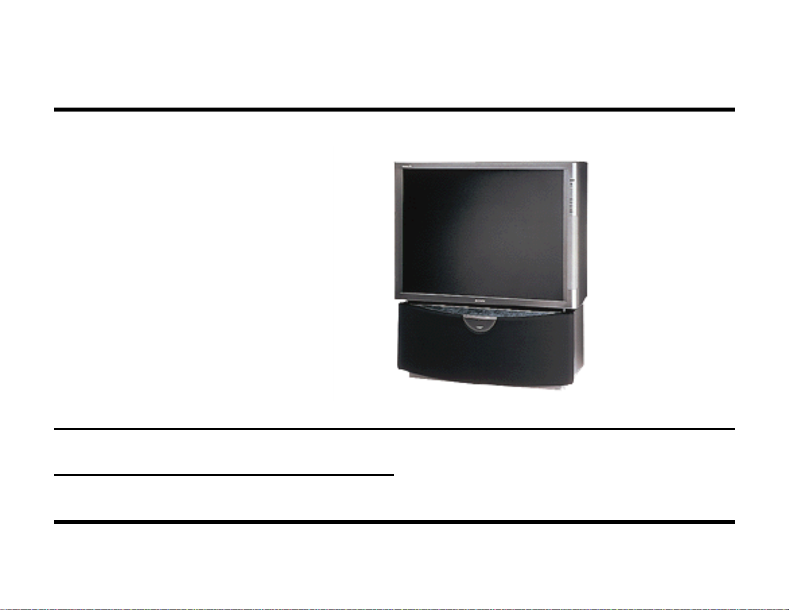
The models covered by this manual are the new KP53XBR200 and the
KP61XBR200. These two models are electrically identical. The differences have to do with screen size. Therefore they use different cabinets,
screens, mirrors and tubes. These sets also have a Self Diagnostic system.
Picture
The two models share the following picture features:
··
· Advanced Pro-Optic System – Sony technology that allows full cor-
··
ner to corner focusing.
··
· New Extended Definition CRT – Allows corner to corner focusing to
··
be increased by 25% over last year’s model.
··
· MICROFOCUS Lens System
··
··
· Digital Reality Creation (DRC) – DRC uses line doubling and pat-
··
tern recognition algorithms to take the NTSC signal to a near HDTV
equivalent. This will be discussed in more detail later.
··
· Double Scan Technology
··
··
· Auto Focus Full Digital Convergence – Allows the setting of V and
··
H center and skew by the customer. This convergence system can
produce a sharper picture and is less susceptible to drift due to aging
or shipment.
··
· High Performance Video Processor
··
··
· 3D Digital Comb Filter
··
··
· Brightview Dual Component Screen – The screen contains a Thin
··
Film Fresnel that brightens and sharpens the picture, and a Fine Pitch
Lenticular screen that achieves higher resolution by using black stripes
to increase contrast.
··
· Built-in High Contrast Screen
··
1
··
· First Surface Mirror – Unlike most mirrors, the reflective surface is
··
on the front of the mirror glass. This improves brightness and contrast, and eliminates ghosting caused by the reflected light passing
through the glass.
··
· Advanced Velocity Modulation
··
··
· Advanced High Voltage Regulation – Eliminates distortion and fo-
··
cus fluctuations that occur when changes in brightness levels cause
changes in the high voltage.
··
· Noise Reduction
··
··
· Shading Compensation – Eliminates color shift and hot spots that
··
can occur due to the angle of the picture tubes to the mirror.
··
· Wideband Video Amplifier
··
··
· Multi Image Driver – Digital-editing technology that provides versatil-
··
ity in controlling on-screen images. Used in Picture and Picture and
Channel Index modes.
··
· Twin View Picture-in-Picture – Allows for viewing two pictures si-
··
multaneously and the ability to expand either image up to double its
normal size.
··
· Free Layout Picture-in-Picture – Allows the PIP window to be placed
··
anywhere on the screen.
··
· XDS (Extended Data Service) – Receives data information services
··
that some stations may broadcast. This data includes time, station
call letters, etc.
Audio
The two models share the following audio features:
··
· MTS Stereo with dbx NR
··
··
· Dolby Pro Logic Surround Sound
··
··
· Front Left/Right Audio Power - 20Wx2
··
··
· Center Audio Power – 20W
··
··
· Surround Audio Power – 15Wx2
··
··
· Center speaker input for use with a separate Dolby Pro Logic A/
··
V Reciever

NOTES
2
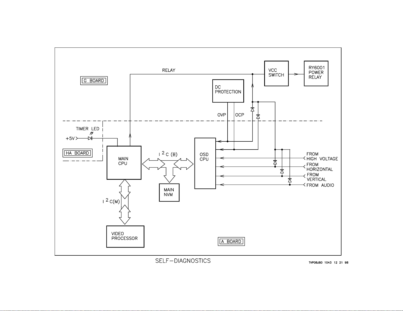
Self-Diagnostics
3
The number of times the LED blinks may correspond to that shown in the
following table:
Overview
The RA-4 chassis employs a Self-Diagnostic system that uses the Timer
LED and an on screen menu to help indicate where the problem with the
set has occurred. You will generally have to use the flashing LEDs since
the set will be shut down. AC power must be disconnected in order to turn
the set off once shutdown has occurred.
When a failure occurs, all of the circuits covered by the Self-Diagnostics,
except AKB, send a signal to the OSD CPU. The OSD CPU sends data
to the Main CPU that indicates how many times the Timer LED will flash.
The AKB circuit located in the Video Processor IC sends data over the
I2C bus directly to the Main CPU. In addition, each circuit, except AKB
and High Voltage, send a signal to the latch circuit to shut the set down
when failure occurs.
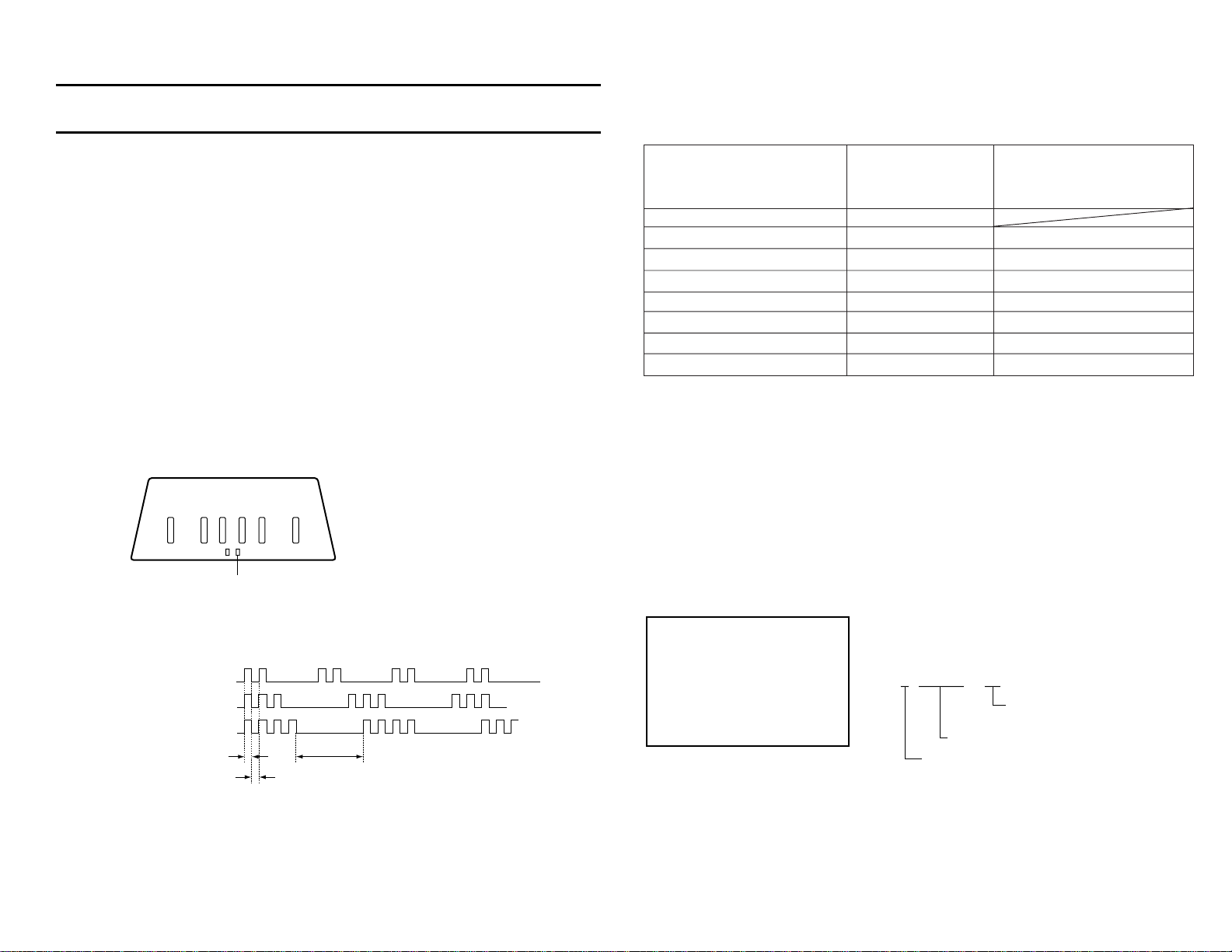
< FRONT PANEL >
TIMER/STANDBY indicator
•EXAMPLE
<Diagnosis Items>
• +B overcurrent
• +B overvoltage
• Vertical deflection stop
Diagnosis item Standby/ Self-diagnosis
sleep lamp, screen display,
Number of blinks Diagnosis item: Results
• Power not ON Not lit
+B OCP detection LED blinks 2 times 2 : +B OCP XX
+B OVP detection LED blinks 3 times 3 : +B OVP XX
V detection LED blinks 4 times 4 : V STOP XX
AKB detection LED blinks 5 times 5 : AKB XX
H detection LED blinks 6 times 6 : H STOP XX
HV abnormality detection LED blinks 7 times 7 : HV XX
Audio abnormality detection LED blinks 8 times 8 : AUDIO XX
: XX the range of values for number of operations is 00-99. For 99 or higher there is no count up
*
and the number remains at 99.
If the problem is intermittent and you can get the set to operate, you can
display a menu showing the number of times failures have occurred. This
is done by pressing the following sequence of buttons on the remote.
Display Channel 5 Vol - Enter
The display will look as follows.
<Number of Blinks>
2 times
3 times
4 times
Lamp ON : 0.3 seconds
Lamp OFF : 0.3 seconds
Lamp OFF :
3.0 seconds
SELF CHECK
2 : +B OCP XX
3 : +B OVP XX
4 : V STOP XX
5 : AKB XX
6 : H STOP XX
7 : HV XX
8 : AUDIO XX
9 : WDT XX
2 : +B OCP XX
Diagnosis
Results
XX the range of values for number of
operations is 00-99.
For 99 or higher there is no count up
and the numberremainsat 99.
4
5
Board Descriptions
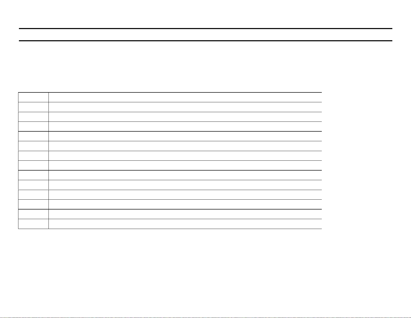
Overview
The models covered by this manual are the new KP53XBR200 and the KP61XBR200. These two models are electrically identical. The differences
have to do with screen size. The table below shows which circuits are present on each of the boards. This will help if you are doing board level (SA YS)
or component level repair.
Name Circuits contained
A Tuners, A/V switching, RGB processing, H Jungle, VDSP, Syscon
BD Auto r e gistration (Digital Convergence)
BM MID (Multi Image Driver)
BR DRC (Digital Reality Creation)
CR,CB,CG CRT drive and IK feedback.
D H and V deflection, Sub-deflection, HV, HV Regulation
G Power supply
HA Front panel controls, Power and Timer LEDs
HB Front video inputs, Auto Focus and Setup buttons
HC Remote sensor
K Audio Processing and Audio Outputs
U S Link Input/Output
ZR,ZG,ZB Hor. and Vert. deflection and sub-deflection coils, VM
CG
ZB
CB
ZG
HC
ZR
HA
CR
HB
K
U
A
G
BM
BD
D
6
BR

7
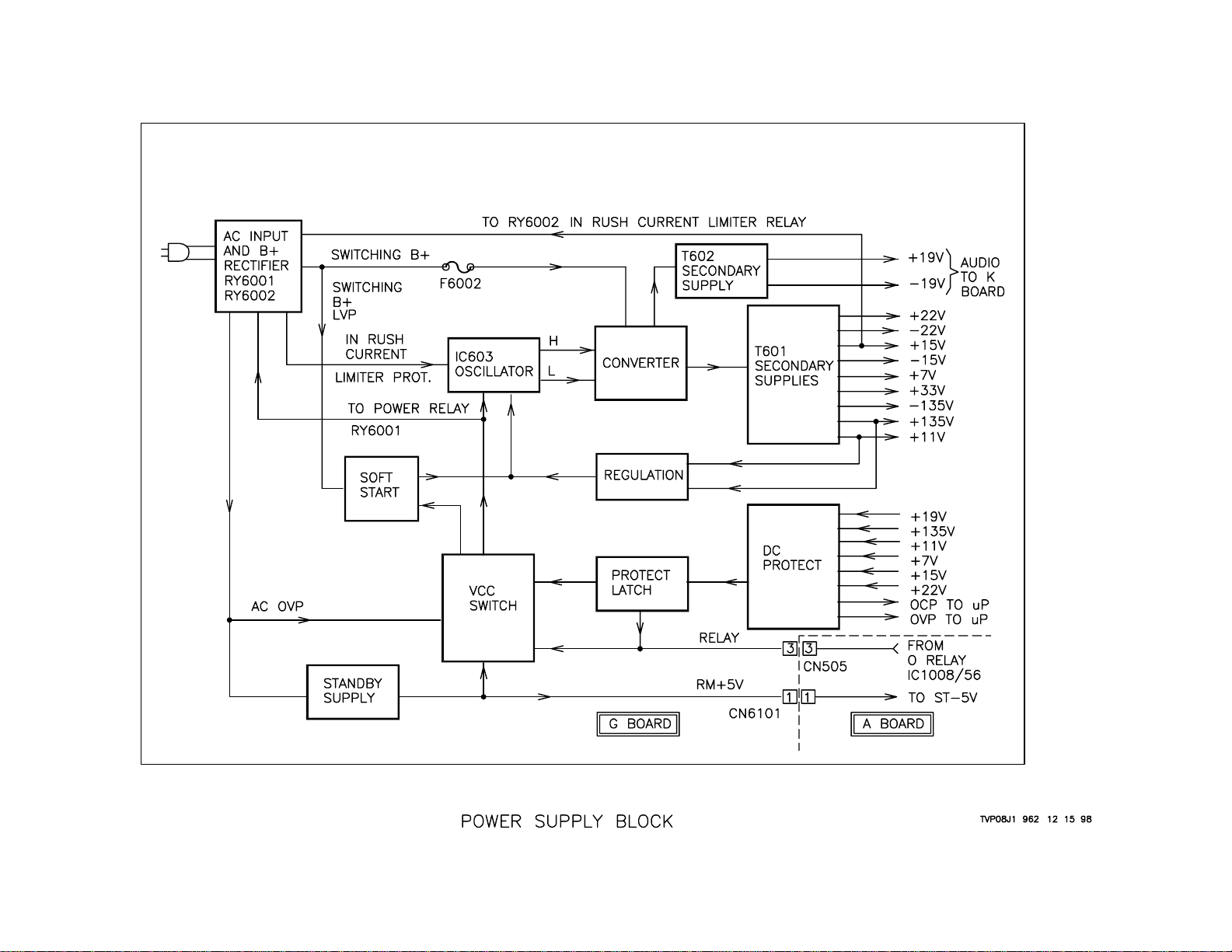
Power Supply Block
AC Input
When the unit is first plugged in, AC power passes through two line filters
and is applied to the Standby Power Supply. This is a switching power
supply that produces the Vcc source voltage and the standby +5V (RM+5V)
for System Control. When the set is turned ON, the AC input is applied
through RY6001 Power Relay to the switching B+ rectifier , which supplies
power to the Converter circuit. The switching B+ rectifier is monitored at
each of its outputs. The negative side of the switching B+ rectifier is monitored to ensure that RY6002 is activated. RY6002 is closed to bypass the
In-Rush Current Limiter Resistor when the set is turned ON. When RY6002
is closed, it shunts In-Rush Current Limiter Resistor so that the negative
side of the bridge is connected to ground. If the relay is not closed, a
voltage will be developed to shut down the set. The positive side of the
switching B+ rectifier is monitored to hold the secondary voltages down if
the AC voltage should be too low. This is performed by monitoring the
switching B+ voltage and applying that voltage to the soft start circuit. This
is done because of the excessive current draw when the switching B+ is
low.
Power ON
When Power ON is selected using the remote or the front panel switch, a
signal is sent from IC1008 Main-CPU to the Vcc switch section on the G
board. The Vcc circuit sends voltage from the Standby supply to the Oscillator and Soft Start circuits. When this voltage reaches IC6003 Oscillator, it begins oscillating. The Soft Start circuit is activated at the same
time. This circuit keeps the oscillator at a certain frequency (175KHz) for
a specified period of time. This keeps the initial start up voltage low and
prevents excessive back EMF from destroying the converter transistors.
When regulation begins, the normal operating frequency is around 73KHz.
Converter
When the Oscillator circuit begins oscillating, it outputs two signals that
are 180 degrees out of phase. These signals are applied to the converter
circuit. The converter circuit contains two Driver ICs that drive two push
pull transistor circuits. These circuits drive two transformers that create
the AC voltages, which are rectified by the two secondary supply circuits
to power the rest of the set.
Regulation
Once the secondary supplies begin to generate DC voltages we can begin to regulate their output. This is done using the +1 1 volt and +135 volt
lines. The +11 volt line is used to power the regulation circuit while the
+135 volt line is monitored to regulate the supplies. The +135 volt line is
sent to the regulation circuit to produce an error voltage that is fed back to
the oscillator circuit. This voltage controls the pulse width and frequency
of the oscillator. Changes in the frequency cause changes in ef ficiency of
the transformers, which in turn cause the voltage to become lower or higher .
Protection
In addition to the three protection circuits on the AC side of the supply,
there are additional circuits on the DC side. The +135V line is checked for
OVP and OCP. If one of these conditions occurs, a voltage is sent to the
protect latch to turn it ON. The latch shuts down the set by turning OFF
the Vcc switch. A voltage is also sent to the System Control circuit for the
self-diagnostic system. In addition, the 11V line is compared to the +19,
+22 and +7 volt lines. If these voltages fall below a specified level, the
protect latch will be activated and the set will shut down. There is no
indication in the self-diagnostic menu that this circuit has been activated.
8

9
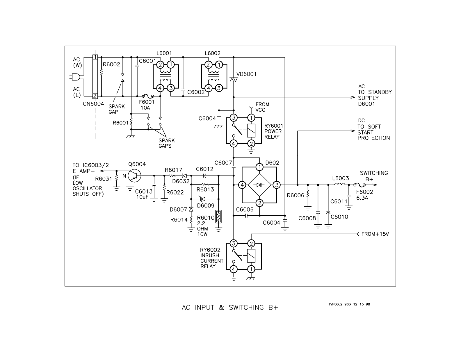
AC Input and Switching B+
Overview
The AC Input and Switching B+ circuit is used to filter the AC line voltage
and generate the DC voltage necessaary to run the switching supply.
AC Input
AC enters the G board at CN6004 when the unit is plugged in. It then
passes through F6001 and L6001 and L6002 Line Filters. L6002/3 is
the High side of the AC line and splits off to two places. It is used to
power the Standby +5V supply and is connected to one of the contacts
of RY6001 Power Relay.
There are a few protection components in place in addition to F6001
Fuse. There are two spark gaps across the AC line at CN6004 AC Input.
There is also one across the AC line after F6001 Fuse. Two capacitors,
C6001 and C6002, are present on either side of L6001 Line Filter. VD6001
is a VDR across the L6002/1 and 3 for spike protection.
Troubleshooting
Problems in this area are usually the result of line spikes or lightning. If
you have a dead set and suspect lightning damage, you should remove
the G board by removing one screw and pulling it out. A quick visual
check can be performed by looking on both sides of the board for burnt
traces or components. If F6001 is open, be sure to check for any burnt
components. If everything looks OK, then check the voltage across
VD6001. If the line voltage is not present there, continue to work your
way back checking across the AC line until you find an open component.
B+ Rectifier
When power is turned ON, the AC line voltage is applied across D602
Bridge Rectifier because RY6001 Power Relay is closed. D602/3 + outputs 130 volts which is filtered by C6008, C6010 and L6003. This voltage is used as the B+ for the switching power supply converter circuit
and is fused by F6002. D602/4 is connected to ground through R6010
In-Rush Current Limiter at initial power ON. When the secondary supplies begin to run, RY6002 will be closed which connects D602/4 - to Hot
ground.
Switching B+ Low Voltage Protect
Both outputs of the D602 Bridge Rectifier are monitored to cause shutdown of the set. D602/3 + has a sample voltage sent to the Soft Start
circuit to monitor for under voltage. If the voltage at this point is too low,
the Soft Start circuit will raise the frequency of the switching supply , thereby
lowering the secondary output voltages and disabling regulation. The
lowering of the secondary voltages will also cause RY6002 to open or
may shut the set down. Due to the fact that the power supply voltages
will be lowered, the set will indicate an AKB shutdown by flashing the
Timer LED five times, pausing, and then repeating. This action will be
discussed in greater detail in the Soft Start section.
In-Rush Current Limiter Protect
D602/4 is monitored to ensure that the R6010 In-Rush Current Limiter
has been switched out of the circuit by RY6002. If it has not, a voltage
will be developed across it that is rectified and sent to the base of Q6004
AC Protect. If Q6004 AC Protect is turned on, IC6003 Oscillator will be
shut down. This will cause no output from the switching supply. Keep in
mind that there will be 150 volts present at F6002 since the power relay
is still turned ON. In addition, the Timer LED will flash twice, pause and
repeat. You will not be able to shut the set OFF using the remote or the
front panel switch. The set will have to be unplugged to attempt to restart the set.
10

11
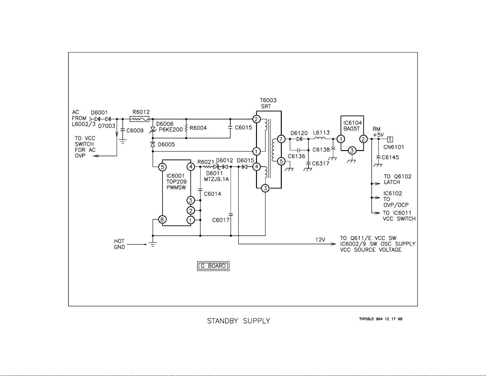
Standby Power Supply
Overview
The Standby Power Supply is used to develop the voltages that are required by the set in order for it to turn ON. One of these voltages is used
to supply power to the System Control ICs. This voltage is a regulated 5
volts and is called RM+5. The other voltage is used as the source voltage for Vcc, which is the low voltage supply for the switching power
supply . The AC input to the standby supply is monitored for overvoltage.
It will shut the Vcc switch OFF if there is a problem.
Standby Switching Supply
The line AC from L6002/3 is rectified by D6001 and D6003 and filtered
by C6009. This voltage is monitored for overvoltage via D6035 and is
used to power the standby supply. This voltage then passes through
fusible resistor R6012, then to T603 SRT. IC6001 is connected to T6003/
1 and begins switching when the voltage arrives. IC6001 PWMSW is a
self-starting N-channel MOSFET switching device with a self contained
oscillator and error loop amplifier used for regulation.
RM+5
As IC6001 PWMSW voltages are induced in the secondary windings of
T6003 SRT, one of these voltages is used to develop the RM+5 line. The
signal from T6003/7 is rectified by D6120 and filtered by C6137, C6138
and L6113. This voltage is input to IC6104/1. IC6104 5-Volt Regulator
outputs 5 volts from pin 2. This is the RM+5 line on the G board. It is
called ST-5V on the A board.
Regulation
The secondary winding at pins 3 and 4 of T6003 SRT develops a voltage
that is rectified by D6015. This voltage is used for two purposes. It is the
source voltage for the Vcc switch and the feedback voltage for regulation. This voltage passes through D6012, D6011 and R6021, and is
input to IC6001/4. Pin 4 is the regulation input for IC6001 PWMSW.
12

13
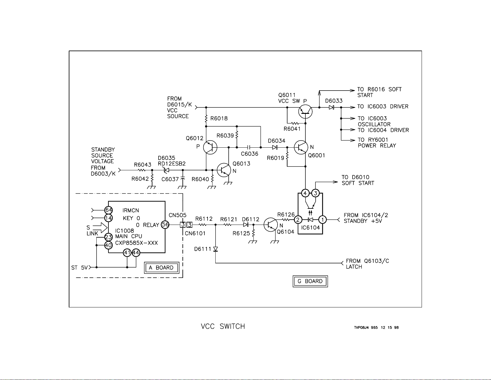
Vcc Switch (Power On)
Overview
When Power On is selected, IC1008 Main CPU sends a signal to the G
board to turn ON the Vcc switch. The Vcc voltage powers the Soft Start,
Oscillator and Driver circuits. There is a connection from the latch circuit
to shut OFF the set if there is a problem on the DC side of the power
supply. In addition, there is a connection from the Standby Source Voltage that will shut down the supply if the AC line voltage becomes to high.
Power ON
When Power ON is selected using either the remote or the front panel
switch, 5 volts is output from IC1008/56 O Relay. This voltage travels
from CN505/3 on the A board to CN6101/3 on the G board. It then goes
through R6112, R6121 and D6112, placing .6V at Q6104/B. This turns
Q6104 ON and causes Q6104/C to pull IC6104/2 to ground. This turns
the phototransistor inside IC6104 Vcc Switch ON. When this occurs,
current flows through the B-E junction of Q6001. When Q6001 turns
ON, it causes Q6011 VccSW to turn ON. This switches the Standby
voltage through Q601 1 VccSW where it is called Vcc. Vcc turns R Y6001
Power Relay ON, as well as powering the Soft Start, Oscillator and Driver
circuits.
DC Protect
The DC protection latch circuit is connected through D6111 to the power
ON line at the junction of R6112 and R6121. When the protection latch
is activated, it pulls the O Relay line LOW and turns power OFF by turning and holding Q6014 OFF.
AC Protect
The Standby Source voltage is monitored in case there is an overvoltage
problem on that line. If the voltage from the Standby Source voltage
goes too high, it will cause the voltage at the cathode of D6035 to rise
above 12.6 volts. The voltage at Q6013/B will be enough to turn it ON.
When this occurs, Q6013 conducts, causing Q6012 to conduct. This
action causes the Q6001 to turn OFF, thereby shutting down the set.
14

15
Soft Start
Overview
A Soft Start circuit is necessary to keep the oscillator that drives the switching circuit above the normal operating frequency of the tuned circuit that
is in the switching supply circuit. If this frequency is not above the normal
operating frequency at start up, the voltage at the secondary could become too high and cause damage to the set. The soft start circuit causes
the oscillator to start at a frequency high above the normal operating frequency by holding the regulating voltage down at initial turn ON of the set.
This circuit is also activated if the Switching B+ voltage falls below a certain level.
Soft Start – Power ON
When Power ON is selected, the Vcc switch supplies voltage to IC6003
Oscillator. This oscillator is connected to the regulation line that begins to
develop voltage. This voltage is held LOW at Q6006/E while C6016 is
charging. Once C6016 is charged, the regulation line is controlled by
IC6005/4.
Q6005 provides a discharge path for C6016 when the set is turned OFF.
This is important because if C6016 is not completely discharged, the oscillator may output the normal operating frequency during Power ON. The
discharge path would be through Q6005/C-E junction. Q6005 is OFF
during the set’s operation because of the voltage applied to it from IC601 1/
3. Be careful when measuring voltages at Q6005/B as this circuit is easily
loaded by a meter or a scope. It is best measured using a scope and a
10X probe.
Soft Start - LVP
The soft start circuit can also be activated if the voltage from D602/3
Switching B+ goes too low. When the voltage across R6007 drops below
12.6 volts, it will cause Q6002 to turn OFF. This causes Q6003 to turn
ON. When Q6003 is ON, the cathode of D6014 will be held at ground
potential. This is the same condition that occurs at turn ON, therefore the
oscillator will oscillate at a high frequency and this will reduce the output
voltages from the secondary supplies. If this occurs while the set is operating, it will shutdown. The set will act as if there was an AKB failure, the
Timer LED will flash five times, pause and then repeat.
16

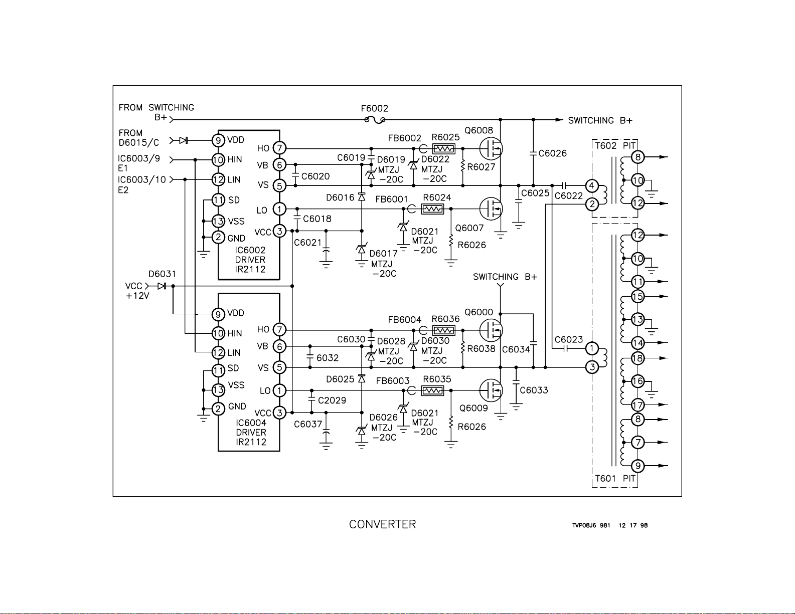
Converter
Overview
Simply put, the converter circuit switches the DC Switching Supply B+ ON
and OFF to create an AC signal. The converter in this set consists of two
Driver ICs that drive two sets of N-channel MOSFET transistors. The
drivers use the output signal from the oscillator to switch the transistors.
These transistors are switched 180 degrees out of phase and are parallel
with the two Power Input Transformers.
Operation
Two signals 180 degrees out of phase are applied to the Hi and Lo side
inputs. The Hi side input of IC6002/10 is the same phase as the Lo side
input at IC6004/12. The Low side input at IC6002/12 is the same phase
as the Hi side input at IC6004/10. These signals are amplified and output
in phase with their inputs.
The Hi side of each of these drivers has a floating power supply that
boosts the output level of the signal. The input to this supply is at IC6002/
6 and IC6004/6. The return is at pin 5 of IC6002 and IC6004. This floating supply allows a 130 Vpp signal to be output for each Hi side driver.
17
If IC6002/7 is outputting a High signal, then Q6008 turns ON. When
Q6008 is ON, it allows the 130-volt Switching B+ to be present at Q6008/
S. This voltage is applied to IC6002/6, the floating supply input, and also
to C6022 and C6023. The signal seeks ground through Q6009, which is
always ON when Q6008 is ON. Current flows through the transformers
T602 and T601 while C6022 and C6023 are charging. At the same time,
the signal outside of IC6002/1 Lo side output is Low. When the signal at
Q6008/G goes Low, the signal at Q6007/G goes High. This causes C6022
and C6023 to be connected to ground. At the same time, Q6010 is turned
ON and Q6009 is turned OFF. This causes current to flow through the
transformers T601 and T602 and capacitors C6022 and C6023. This
cycle continues while the set is running and causes sine waves to be
seen at T601/1 and T602/4. This signal is induced into the secondary of
the transformers to produce the power supply output.
18

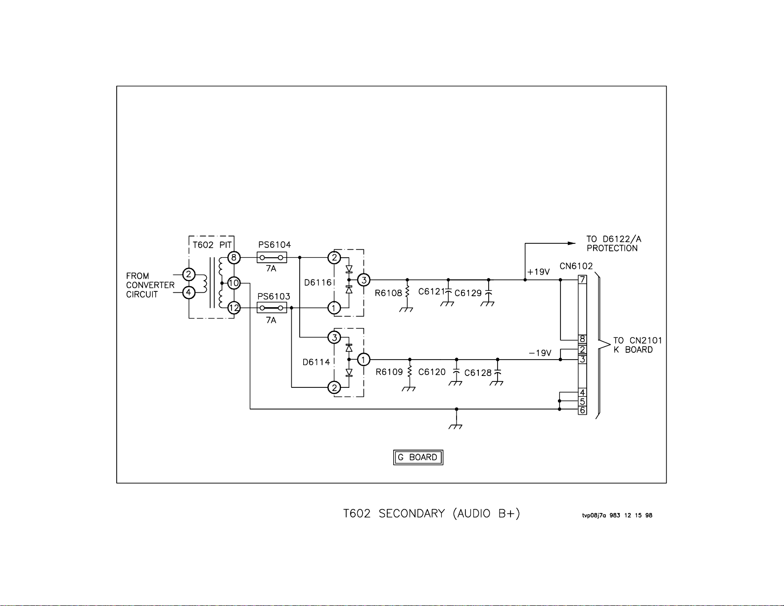
T602 Secondary (Audio B+)
Overview
The secondary winding of T602 PIT is used to develop two voltages - +/19 volts. These voltages are used to power the K board, which contains
all of the audio circuits.
Operation
The voltage induced into the secondary winding of T602 is used to develop +/- 19 volts. This voltage is used to supply the Audio section (K
board) and is fused with PS6103 and PS6104.
This voltage is rectified by D6116 and filtered by C6121 and C6129 to
create the +19 volt supply. It is also rectified by D6114 and filtered by
C6120 and C6128 to create the –19 volts. The +19 volt supply is output
at CN6102/7 and 8. It also goes to D6122/A, which is part of the protection circuitry. The –19 volt supply is output at CN6102/2 and 3.
19
Troubleshooting
If the rest of the power supply is working, but there is a problem with these
supplies, you should suspect a problem on the K board. The set can be
run with CN6102 unplugged. If the correct voltages are measured at
CN6102, then the problem is on the K board. If PS6104 and PS6103 are
open, it would be a good idea to power the unit without CN6102 disconnected. If everything appears to be OK, check the K board for shorts on
the +/- 19 volt lines. If none are found, then plug CN6102 in and power up
the unit.
20
21
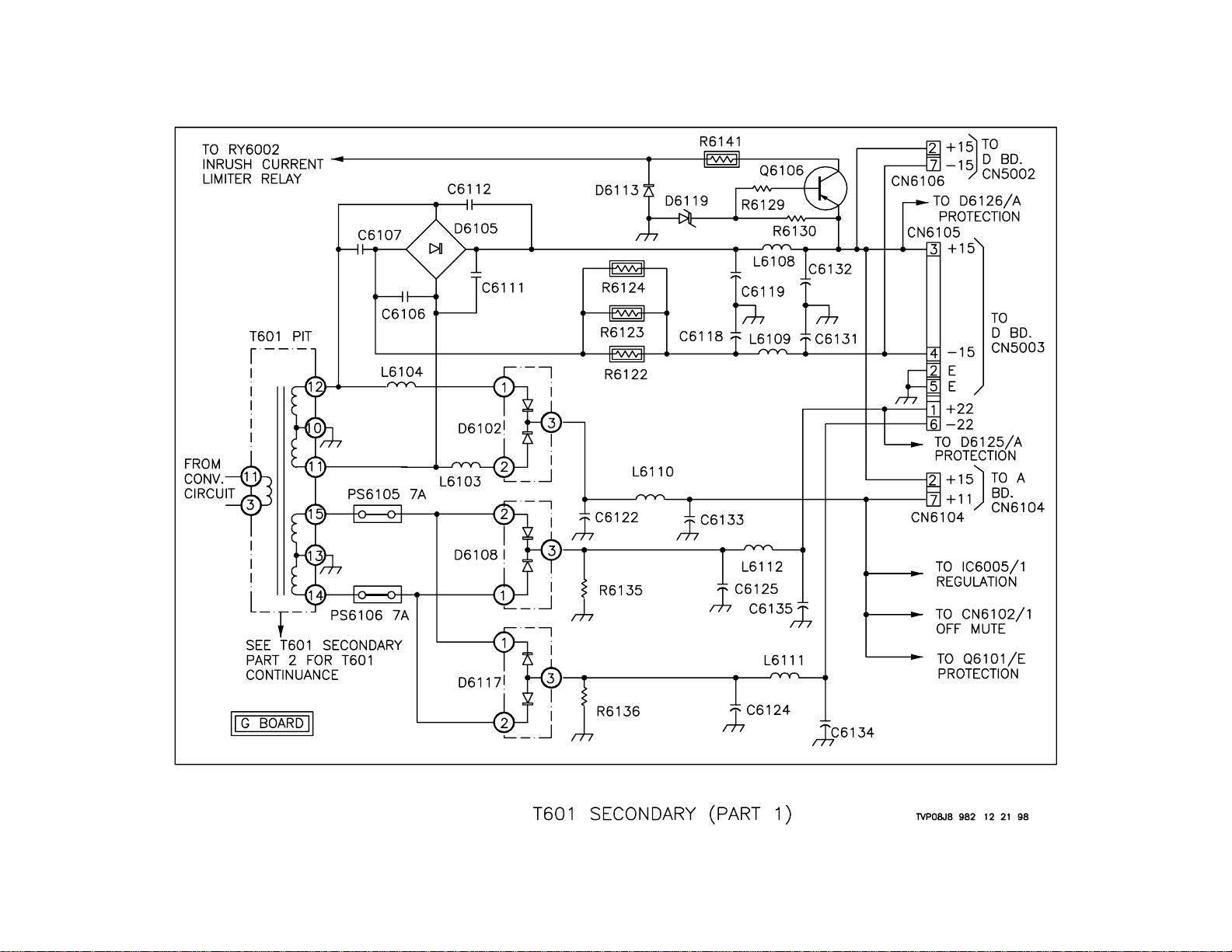
T601 Secondary-1
Overview
There are four secondary windings on T601 PIT. The voltages induced in
these windings are used to power everything in the set, except for the
audio section. The voltages developed here are +/- 15 volts, +/- 22 volts,
+11 volts, +7 volts, +/- 135 volts and +33 volts.
+/- 15 Volts
The voltage from the winding of T601/1 1 and 12 is applied across D6105
Bridge Rectifier. C6119, C6132 and L6108 filter the positive output of
D6105/3. This output is used for three things. First, it is applied to Q6106/
E, which turns Q6106 ON and allows current to flow through its E-C junction. It passes through R6141 to RY6002 In Rush Current Limiter Relay.
It turns the relay ON when the voltage is sufficient. If the voltage does not
rise to a sufficient level or there is a problem with Q6106, the set will shut
down. Next it is sent to D6126/A, which is part of the protection circuitry .
Lastly it is sent to CN6105/3, CN6106/5 and CN6104/2 where it is sent to
the D and A boards.
The negative output from D6105/3 goes through R6122, R6123 and R6124,
which are parallel. C61 18, C6131 and L6109 then filter this voltage. It is
then output from CN6105/4 and CN6106/6, both of which go to the D
board.
These lines are used to produce other voltages on the D board. These
voltages are +/- 12 volts and +/- 5 volts.
+ 11 Volts
The voltage from the winding of T601/1 1 and 12 is applied across D6102
through L6103 and L6104. C6122, C6133 and L6110 filter the rectified
voltage. This voltage is used on the G board by the regulation and protection circuits and it exits the G board at CN6104/11 to the A board.
+/- 22 Volts
The voltage from the winding of T601/14 and 15 is applied across D6108
through PS6105 and PS6106. C6125, C6135 and L6112 filter the rectified voltage. The voltage is used on the G board by the protection circuit
and it exits the G board at CN6105/1.
The winding of T601/14 and 15 is applied across D61 17 through PS6105
and PS6106. C6124, C6134 and L6111 filter the rectified voltage which
leaves the G board at CN6105/6.
The +/- 22volt lines are used to power only the Convergence amplifiers on
the D board.
Distribution
The table below shows the circuits powered by the voltages previously
discussed:
Supply Circuits
+15
-15
+12(D)
+12V(A)
-12
+5
-5
+11
+9
+22
-22
Vertical Out IC5004, 12 Volt regulator IC5002 (D board), IC502 12
Volt regulator (A board)
Vertical Out IC5004, -12 Volt regulator IC5001
V, H, B+, HV, and IK protection circuits, Shading, HV control, PWM,
H Saw, Auto Registration sense and switching, 5 Volt regulator
IC8004
H Jungle IC507, VM and IK buffers
Shading, HV control, H Saw, H pulse shaper,-5 Volt regulator IC8003
BD board (Auto Registration)
BD board (Auto Registration)
Off Mute Q547, 9 Volt regulator IC505
TU501, TU502 Video Processing, AVU switch
Convergence Amplifiers IC5005 and IC5006
Convergence Amplifiers IC5005 and IC5006
The +1 1 volt supply is used on the A board to produce the +9 volt supply.
22
 Loading...