

Sony TASA-100-WR Service manual
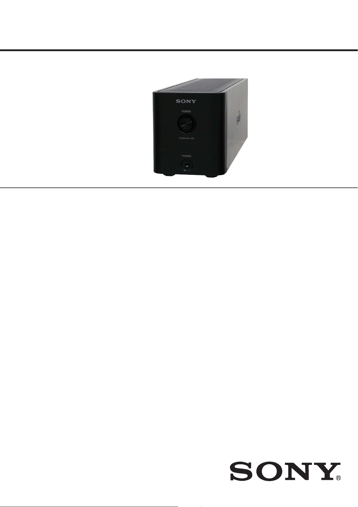
TA-SA100WR
SERVICE MANUAL
Ver. 1.0 2008.02
• TA-SA100WR is the surround amplifi er section
in WAHT-SA1 etc.
• EZW-RT10 or EZW-T100 is necessary to check
S-AIR communication.
SPECIFICATIONS
AUDIO POWER SPECIFICATIONS
for the US model
POWER OUTPUT AND TOTAL
HARMONIC DISTORTION:
With 3 ohm loads,
both channels
driven, from 120 20,000 Hz; rated 50
watts per channel
minimum RMS
power, with no
more than 0.7 %
total harmonic
distortion from 250
milliwatts to rated
output.
Amplifier section
US model:
Surround mode (reference) RMS output power
: 143W (per
channel at 3 ohms,
1 kHz, 10 % THD)
Other models:
Stereo mode (rated) 80 W + 80 W (at
3 ohms, 1 kHz, 1%
THD)
Surround mode (reference) RMS output power
: 143 W (per
channel at 3 ohms,
1 kHz, 10 % THD)
* Depending on the source, there may be no
sound output.
Canadian Model
General
Power requirements:
NorthAmericanmodels: 120VAC, 60Hz
Mexican model: 120 V AC, 60 Hz
Other models: 220 V – 240 V AC,
Power consumption On: 50 W
Dimensions (approx.) 85 mm× 100 mm ×
Mass (approx.) 1.7 kg (3 lb 12 oz)
Design and specifications are subject to change
without notice.
“S-AIR” and its logo are trademarks of Sony
Corporation.
50/60 Hz
330 mm
3
(3
/8 in×4in×
13 in) (w/h/d) (incl.
EZW-RT10)
85 mm × 100 mm ×
345 mm
3
(3
/8 in×4in×
5
13
/8 in) (w/h/d)
incl. speaker cord
cover and speaker
cord holder
incl. speaker cord
cover and speaker
cord holder
US Model
AEP Model
UK Model
E Model
9-887-986-01
2008B05-1
2008.02
©
Rated impedance: 3 - 16 Ω
SURROUND AMPLIFIER
Sony Corporation
Audio Business Group
Published by Sony Techno Create Corporation
TA-SA100WR
• Never reuse a disconnected chip component.
• Notice that the minus side of a tantalum capacitor may be damaged by heat.
SAFETY CHECK-OUT
After correcting the original service problem, perform the following safety check before releasing the set to the customer:
Check the antenna terminals, metal trim, “metallized” knobs,
screws, and all other exposed metal parts for AC leakage.
Check leakage as described below.
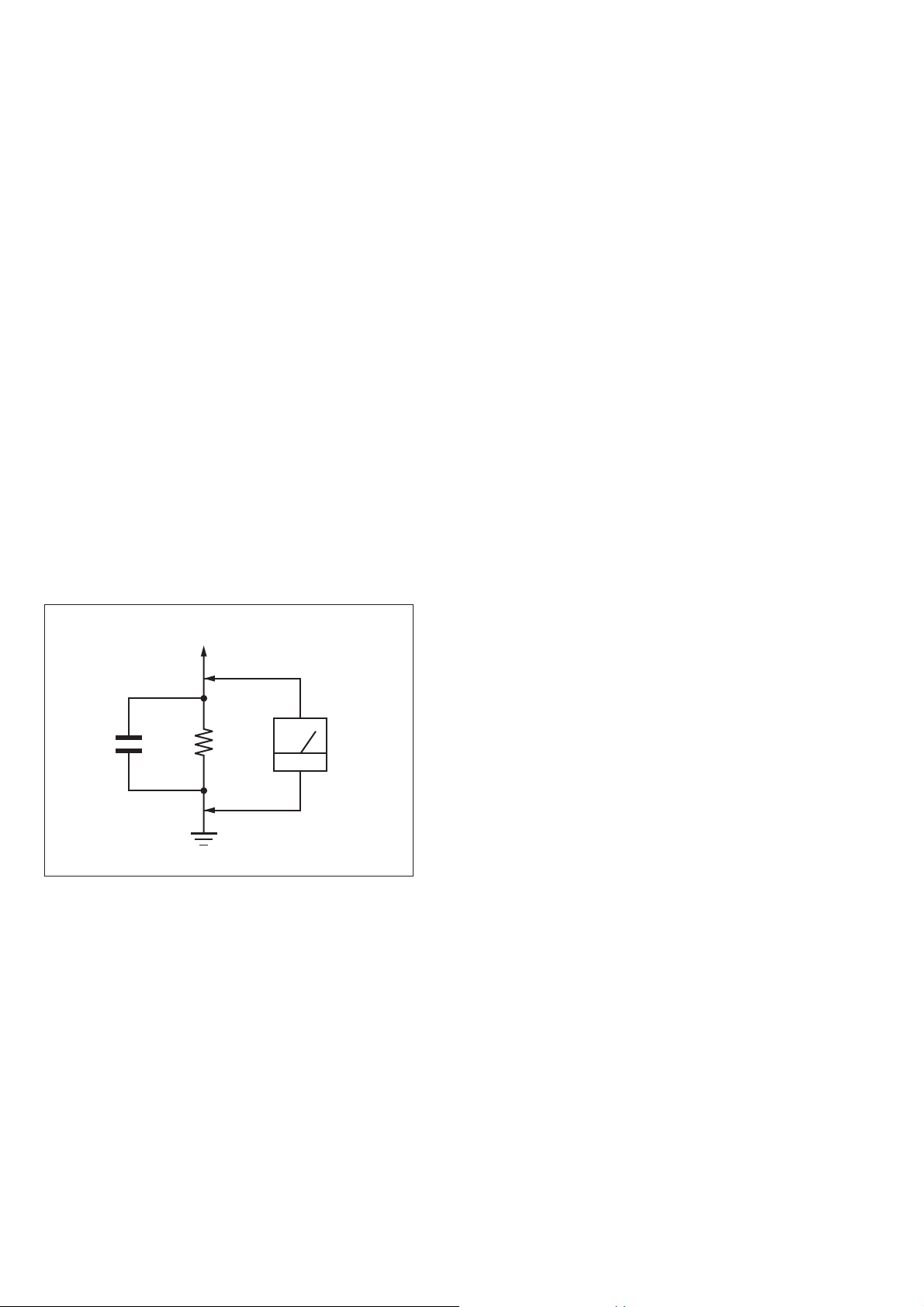
LEAKAGE TEST
The AC leakage from any exposed metal part to earth ground and
from all exposed metal parts to any exposed metal part having a
return to chassis, must not exceed 0.5 mA (500 microamperes.).
Leakage current can be measured by any one of three methods.
1. A commercial leakage tester, such as the Simpson 229 or RCA
WT-540A. Follow the manufacturers’ instructions to use these
instruments.
2. A battery-operated AC milliammeter. The Data Precision 245
digital multimeter is suitable for this job.
3. Measuring the voltage drop across a resistor by means of a
VOM or battery-operated AC voltmeter. The “limit” indication
is 0.75 V, so analog meters must have an accurate low-voltage
scale. The Simpson 250 and Sanwa SH-63Trd are examples
of a passive VOM that is suitable. Nearly all battery operated
digital multimeters that have a 2 V AC range are suitable. (See
Fig. A)
To Exposed Metal
Parts on Set
TABLE OF CONTENTSNotes on chip component replacement
1. SERVICIN NOTES ................................................. 3
2. GENERAL .................................................................. 6
3. DISASSEMBLY
3-1. Disassembly Flow ........................................................... 7
3-2. Cover (Cord) ................................................................... 7
3-3. Case ................................................................................. 8
3-4. Shield (Top), Power Cord ............................................... 8
3-5. Power SW Board, PANEL Board, Front Panel Block .... 9
3-6. Back Panel, JOINT Board ............................................... 9
3-7. Power Block .................................................................... 9
3-8. POWER Board, AMP Board ........................................... 9
4. DIAGRAMS
4-1. Block Diagram ................................................................ 10
4-2. Printed Wiring Board
- AMP Board (Component Side) (Suffi x-11) - ................ 12
4-3. Printed Wiring Board
- AMP Board (Conductor Side) (Suffi x-11) - ................. 13
4-4. Printed Wiring Board
- AMP Board (Component Side) (Suffi x-12) -................ 14
4-5. Printed Wiring Board
- AMP Board (Conductor Side) (Suffi x-12) - ................. 15
4-6. Schematic Diagram - AMP Board (1/2) - ....................... 16
4-7. Schematic Diagram - AMP Board (2/2) - ....................... 17
4-8. Printed Wiring Boards - PANEL Section - ..................... 18
4-9. Schematic Diagram - PANEL Section - .......................... 19
4-10. Printed Wiring Boards - POWER Section - .................... 20
4-11. Schematic Diagram - POWER Section - ........................ 21
AC
1.5 kΩ0.15 μF
Earth Ground
voltmeter
(0.75 V)
Fig. A. Using an AC voltmeter to check AC leakage.
SAFETY-RELATED COMPONET WARNING!
COMPONENTS IDENTIFIED BY MARK 0 OR DOTTED LINE
WITH MARK 0 ON THE SCHEMATIC DIAGRAMS AND IN
THE PARTS LIST ARE CRITICAL TO SAFE OPERATION.
REPLACE THESE COMPONENTS WITH SONY PARTS
WHOSE PART NUMBERS APPEAR AS SHOWN IN THIS
MANUAL OR IN SUPPLEMENTS PUBLISHED BY SONY.
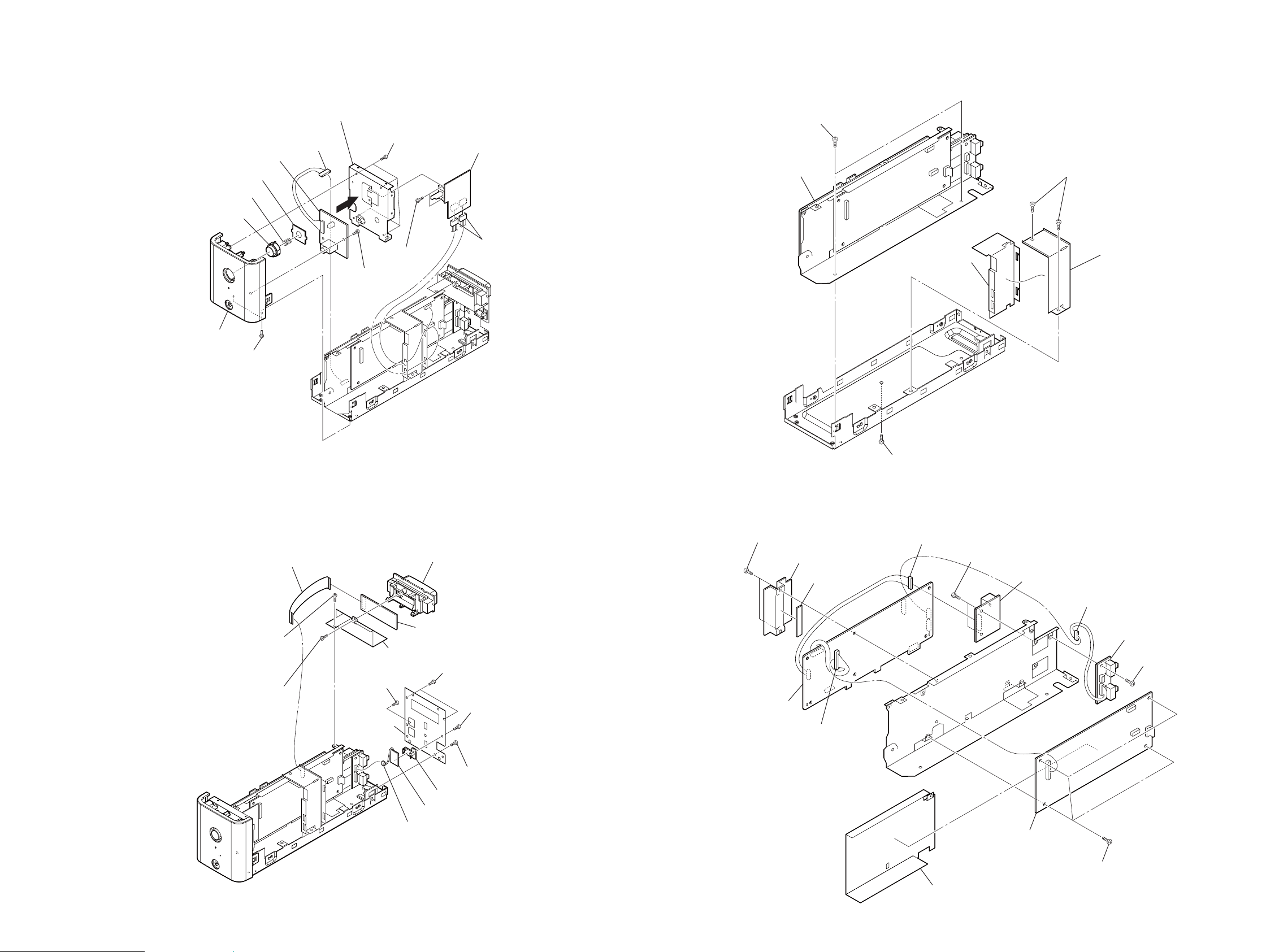
5. EXPLODED VIEWS
5-1. Cover Section .................................................................. 26
5-2. Top Shield Section .......................................................... 27
5-3. Front Panel Section ......................................................... 28
5-4. Chassis Section ............................................................... 29
5-5. Power Section ................................................................. 30
6. ELECTRICAL PARTS LIST .............................. 31
ATTENTION AU COMPOSANT AYANT RAPPORT
À LA SÉCURITÉ!
LES COMPOSANTS IDENTIFIÉS PAR UNE MARQUE 0 SUR
LES DIAGRAMMES SCHÉMATIQUES ET LA LISTE DES
PIÈCES SONT CRITIQUES POUR LA SÉCURITÉ DE FONCTIONNEMENT. NE REMPLACER CES COM- POSANTS QUE
PAR DES PIÈCES SONY DONT LES NUMÉROS SONT DONNÉS DANS CE MANUEL OU DANS LES SUPPLÉMENTS
PUBLIÉS PAR SONY.
2
SECTION 1
SERVICING NOTES
TA-SA100WR
UNLEADED SOLDER
Boards requiring use of unleaded solder are printed with the leadfree mark (LF) indicating the solder contains no lead.
(Caution: Some printed circuit boards may not come printed with
the lead free mark due to their particular size)
: LEAD FREE MARK
Unleaded solder has the following characteristics.
• Unleaded solder melts at a temperature about 40 °C higher
than ordinary solder.
Ordinary soldering irons can be used but the iron tip has to be
applied to the solder joint for a slightly longer time.
Soldering irons using a temperature regulator should be set to
about 350 °C.
Caution: The printed pattern (copper foil) may peel away if the
heated tip is applied for too long, so be careful!
• Strong viscosity
Unleaded solder is more viscous (sticky, less prone to fl ow)
than ordinary solder so use caution not to let solder bridges
occur such as on IC pins, etc.
• Usable with ordinary solder
It is best to use only unleaded solder but unleaded solder may
also be added to ordinary solder.
Checking the transmission status
You can check the status of sound transmission between the S-AIR main
unit and surround amplifier by checking the POWER/ON LINE indicator
on the surround amplifier.
SUFFIX-11/SUFFIX-12 DISCRIMINATION OF AMP BOARD
– AMP Board (Component Side) –
IC500
Suffix-11 : 1-875-376-11
Suffix-12 : 1-875-376-12
POWER/ON
LINE indicator
Turns green Sound transmission is established.
Flashes green Sound transmission is not established. Fordetails, see
Turns red The surround amplifier does not output sound. For details,
Turns off The surround amplifier turns off or its protection is active.
Status
“Troubleshooting”.
see “Troubleshooting”.
For details, see “Troubleshooting”.
Troubleshooting
Sound
There is no sound.
Check the status of the POWER/ON LINE indicator on the surround
amplifier.
– turns green
• The speaker cord is not connected securely.
• Check the speaker connections and settings.
• The volume of the S-AIR main unit is set to minimum.
• The S-AIR main unit is in mute status.
• Depending on the source or thesettings of the S-AIR main unit, the effect of the
speakers may be less noticeable.
• Headphones are connected.
– flashes green
• The S-AIR main unit is not turned on.
• The S-AIR main unit is paired to another S-AIR product.
• The surround amplifier is paired to another S-AIR main unit.
• Confirm the IDs of the S-AIR main unit and surround amplifier.
• Pairing operation is not completed.
• Sound transmission is poor. Move the
surround amplifier so that the POWER/ON LINE indicator turns green.
• Move the system away from any other wireless products.
• Stop using another wireless product.
• The wireless transceiver and/or the wireless transmitter are/is not inserted
correctly.
– turns red
• Change the SURROUND SELECTOR switch (SURROUND or SURROUND
BACK) of the surround amplifier to match the S-AIR main unit.
3
TA-SA100WR
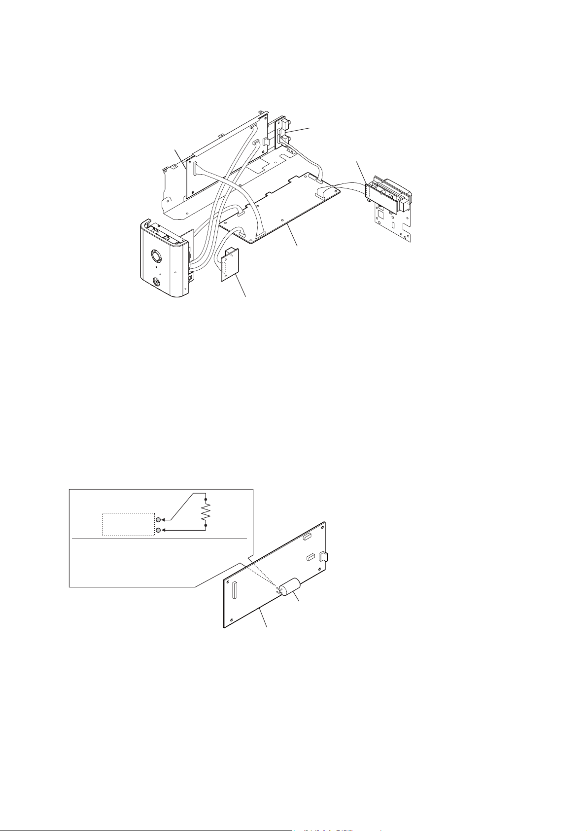
AMP BOARD SERVICE POSITON
POWER board
MODE SW board
JOINT board
AMP board
SP TERM board
CAPACITOR DISCHARGE
C906 or C919
In checking the POWER board,
make a capacitor discharge
of C906 or C919 for electric shock
prevention.
800 Ω/2W
C906 (AEP, UK, E3, MX)
C919 (US, CND)
POWER board
• Abbreviation
CND : Canadian model
E3 : 240V AC area in E model
MX : Mexican model
4
HARNESS SETTING
TA-SA100WR
power cord
holder (P-cord)
clamp
sheet (power-top)
5
TA-SA100WR
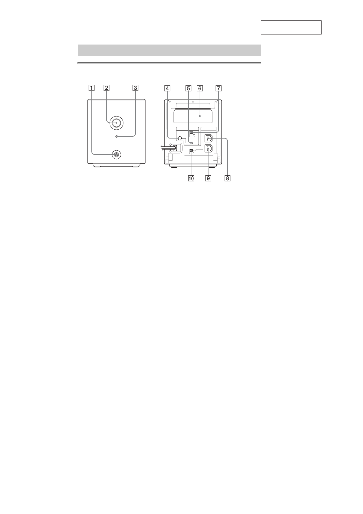
Index to Parts
Surround amplifier
Front panel
POWER
SECTION 2
GENERAL
Rear panel
This section is extracted
from instruction manual.
EZW-RT10
POWER/ON LINE
PHONES
A PHONES jack
B POWER button (ON/OFF)
C POWER / ON LINE indicator
D PAIRING indicator
E PAIRING button
F Wireless transceiver (EZW-RT10) slot
G S-AIR ID switch
H SPEAKER L jack
I SPEAKER R jack
J SURROUND SELECTOR switch
S-AIR ID
PAI RI N G
SURROUND SELECTOR
A
B
C
SURROUND
SURROUND
BACK
SPEAKER
L
R
6
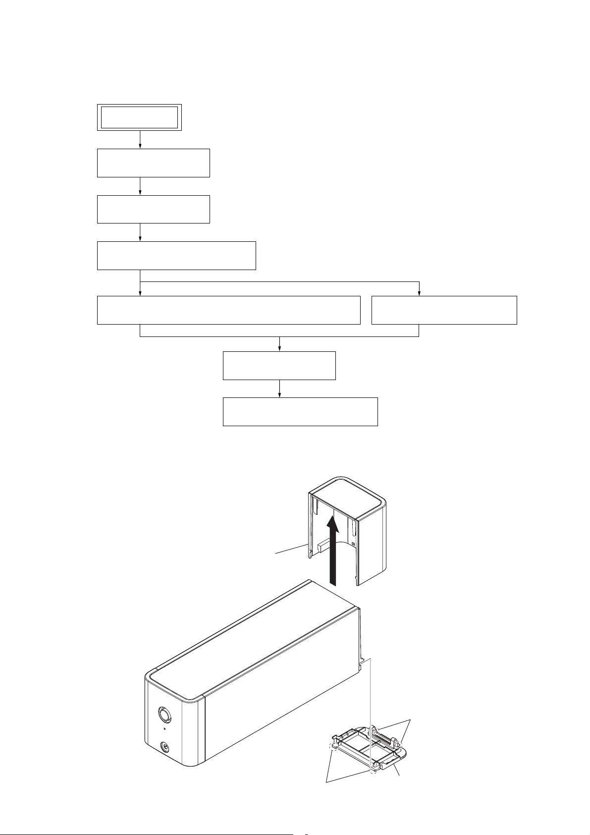
DISASSEMBLY
• This set can be disassembled in the order shown below.
3-1. DISASSEMBLY FLOW
SET
3-2. COVER (CORD)
(Page 7)
3-3. CASE
(Page 8)
3-4. SHIELD (TOP), POWER CORD
(Page 8)
TA-SA100WR
SECTION 3
3-5. POWER SW BOARD, PANEL BOARD, FRONT PANEL BLOCK
(Page 9)
3-7. POWER BLOCK
(Page 9)
3-8. POWER BOARD, AMP BOARD
(Page 9)
Note: Follow the disassembly procedure in the numerical order given.
3-2. COVER (CORD)
cover (cord)
3-6. BACK PANEL, JOINT BOARD
(Page 9)
two claws
two claws
bottom cover (cord)
7
TA-SA100WR
3-3. CASE
screw
(BVTT3 × 6)
four claws
case
four claws
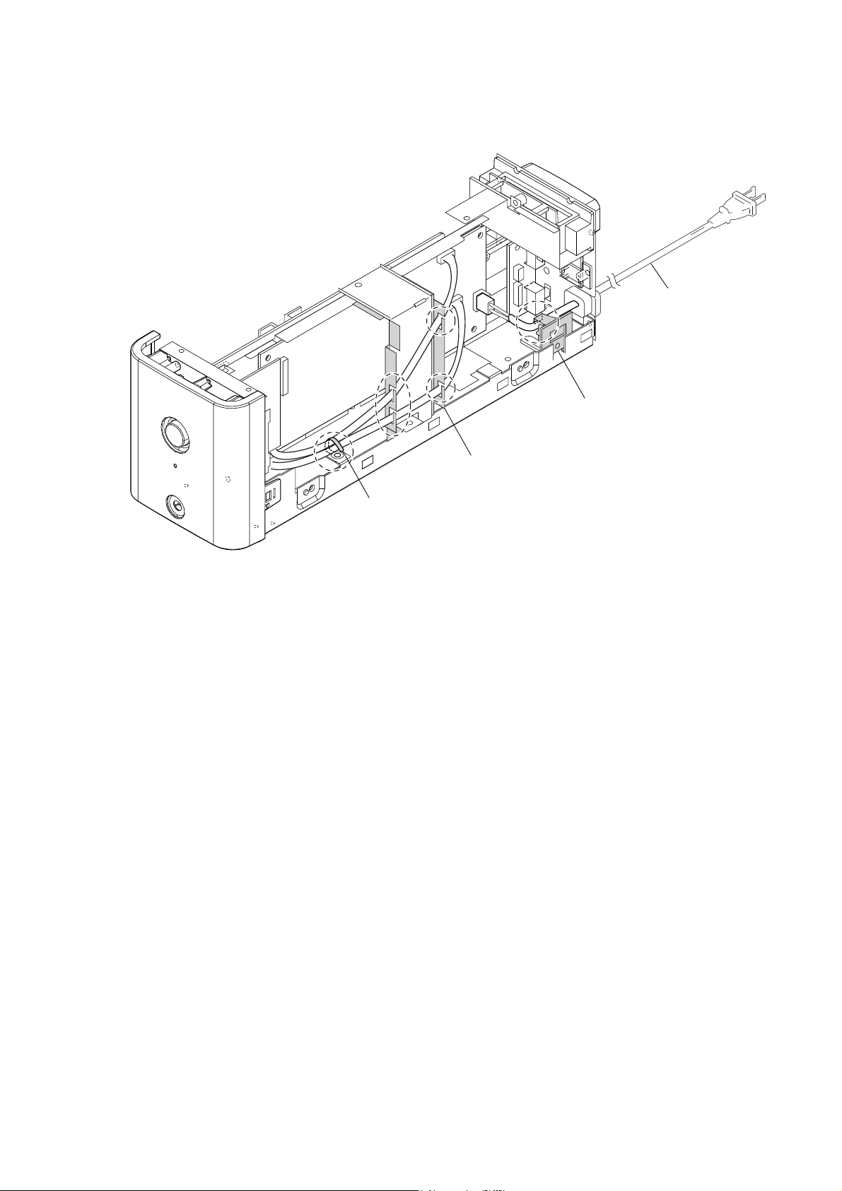
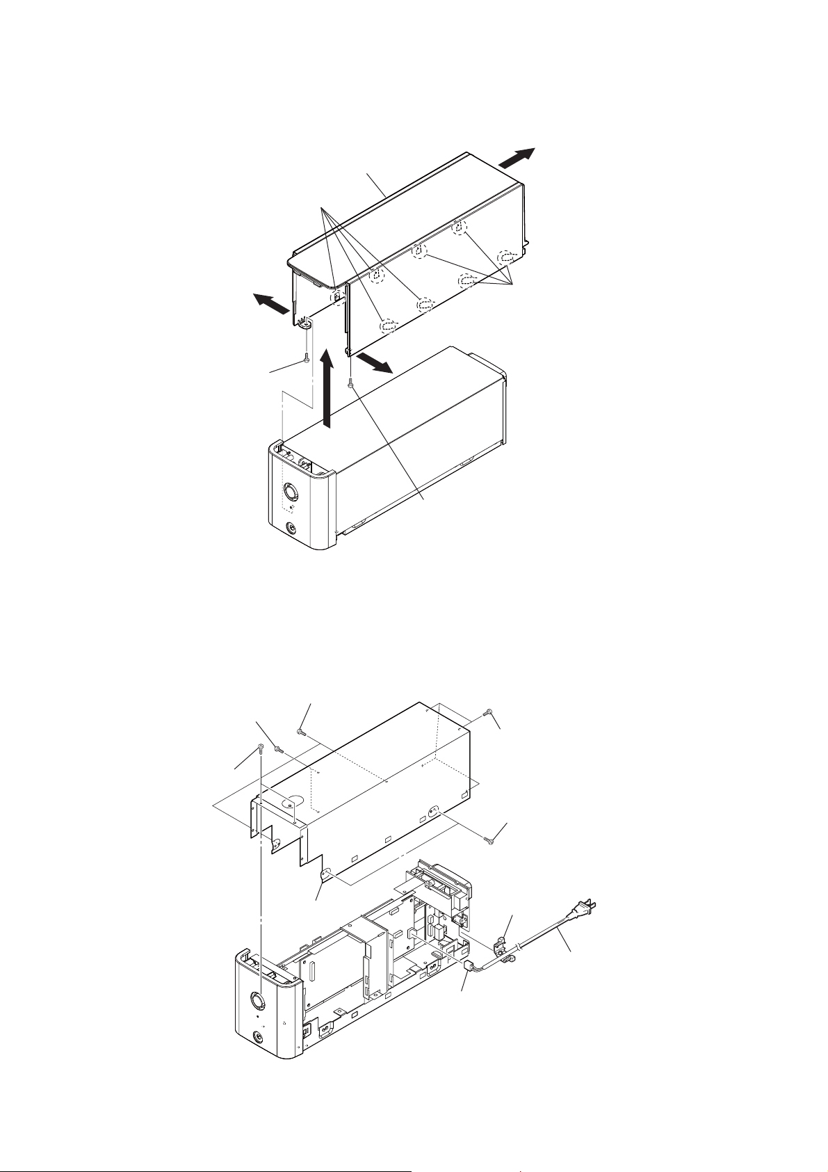
3-4. SHIELD (TOP), POWER CORD
two screws
(BV3)
two screws
(BV3)
two screws
(BV3)
shield (top)
screw
(BVTT3 × 6)
four screws
(BV3)
two screws
(BV3)
cord bushing
power cord
connector
(CN901)
8
TA-SA100WR
TA-SA100WR
99
3-5. POWER SW BOARD, PANEL BOARD, FRONT PANEL BLOCK
3-6. BACK PANEL, JOINT BOARD
3-7. POWER BLOCK
3-8. POWER BOARD, AMP BOARD
shield (front)
four screws
(BVTP2.6)
screw
(BVTP2.6)
two screws
(DIA. 2.6)
bracket (button)
RB
spring (button)
RT
button (power)
RE
front panel block
RG
PANEL board
two screws
(BVTT3 × 6)
connector
(CN301)
POWER SW board
two connectors
(CN905, CN906)
(BV3)
power block
two screws
sheet (power-top)
two screws
(BV3)
bracket (POW)
flexible flat cable
(CN507: JOINT board/CN500:AMP board)
screw
(BVTP3 × 8)
screw
RB
(BVTP3 × 10)
screw
(BVTP3 × 8)
back panel
holder (S-AIR)
RE
JOINT board
RG
shield (S-AIR)
RT
connector
(CN509)
two screws
(BVTP3 × 10)
screw
(BVTP3 × 10)
screw
(BVTP3 × 8)
holder (LED)
LED board
two screws (BVTP3 × 8)
RB
heat sink (AMP)
RT
radiation sheet
RE
AMP board
RG
connector
(CN400)
screw
(BVTT3 × 6)
connector (CN302)
two screws
(BV3)
SP TERM board
POWER board
connector (CN501)
MODE SW board
screw
(BV3)
four screws
(BV3)
sheet (power)
TA-SA100WR
TA-SA100WR
1010
4-1. BLOCK DIAGRAM
SECTION 4
DIAGRAMS
• SIGNAL PATH
: AUDIO
/RESET
/SD
5 4
POWER DRIVER
IC100
POWER DRIVER
IC200
14
PWM_B
6
PWM_A
6
PWM_A
14
PWM_B
TB300
(–)
(+)
OUT_B
OUT_A
STREAM PROCESSOR
IC300
DATA
BCK
LRCK
23
SCLATCH
19
SOFTMUTE
21
SCDT
36
XFSIIN
22
SCSHIFT
6
OUTR1
9
OUTL2
4
OUTR2
11
OUTL1
OVER LOAD
DETECT
Q100, 101
/RESET
/SD
5 4
(+)
(–)
OVER LOAD
DETECT
Q200, 201
SURROUND AMP CONTROLLER
IC500
48
XFSOIN
49
DRIVER_RST(EN)
73
DRIVER_SD
50
DC_DET
20
AC_CUT
12
RESET
SPEAKER
PHONES
14
XFSOOUT
DC DETECT
Q350
OSC
IC301
X300
49.1MHz
35
DAMP_SCDT
37
DAMP_SHIFT
44
DAMP_LATCH
45
DAMP_SOFTMUTE
DAMP_OVF
X500
5MHz
Xout
Xin
27
LED_RED
26
LED_GREEN
D580
POWER/ON LINE
LPF
LPF
LPF
LPF
28 – 30
25 – 27
OUT_A
OUT_B
25 – 27
28 – 30
42DAMP_INIT
27
INIT
1
POWER CONTROL
IC901
D
(AC IN)
F901
TH901
POWER
TRANSFORMER
T901
D911
D908
D910
D907, 909
RECT
D901
LINE
FILTER
ISOLATOR
PC903
OVER LOAD
PROTECT
Q902, 903
4
VCC
7
OCP/BD
5
OLP/SS
ISOLATOR
PC902
TH902
RECT
D921
+32V
+12V
REGULATOR
Q901
ISOLATOR
PC901
6
FB
AC CUT
Q576
PROTECTOR
Q355
RESET SWITCH
Q575
LED DRIVE
Q580, 582
LED DRIVE
Q581, 583
RESET SIGNAL
GENERATOR
IC501
SHUNT
REGULATOR
IC905
+12V
REGULATOR
IC400
VCC2
+3.3V
+1.8V
+1.8V
REGULATOR
IC403
+5V
REGULATOR
IC401
+3.3V
REGULATOR
IC402
53
P_CONT1(MAIN)
S901
POWER
HP_AMP B+
+12V
REGULATOR
IC404
POWER DETECT
Q351, 352
88
PAIRING LED
LED DRIVE
Q560, 561
D560
PAIRING
S503
PAIRING
S502
S-AIR ID
15 13
74
POWER DET
41
P_CONT3(HP)
MUTING
Q170, 171
MUTING
Q270, 271
MUTING
CONTROL
Q370
J300
HEADPHONE
AMP
IC302
41
HPOUTR1
43
HPOUTL2
39
HPOUTR2
45
HPOUTL1
40
HP_SW
39
HP_MUTE
24
FLAGR
25
FLAGL
43
EEPROM
IC502
83
EEP_SDA
82
EEP_SCL
81
EEP_WP
7
WP
5
SDA
6
SCL
D-FLIP-FLOP
IC303
R
L
A
B
C
30 S-AIR_DATA
29 S-AIR_CLK
79 S-AIR_RESET
90 S-AIR_ID_SW
79 SUR_MODE_SW
72 S-AIR_GPIO1
75 S-AIR_GPIO2
31
30
29
S501
SPEAKER
SURROUND SELECTOR
SURROUND
SURROUND BACK
(EZW-RT10)
WIRELESS
TRANSCEIVER
DIND_DOUTB
BCK
LRCK
MCK
I2C_SDA
I2C_SCL
RESN
GPIO1_ASIC_LINK
GPIO2_ASIC_LINK
TA-SA100WR
TA-SA100WR
1111
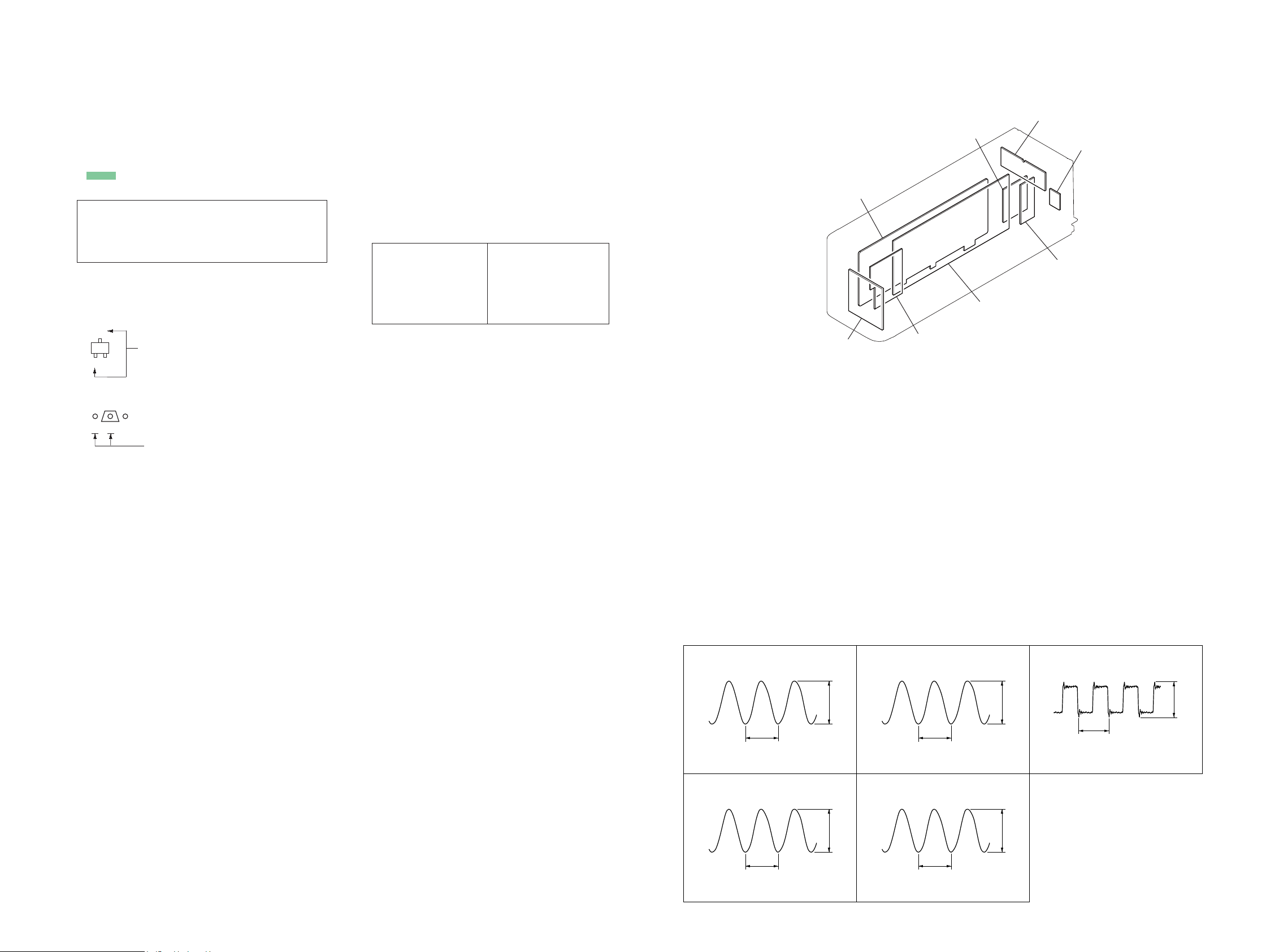
For Schematic Diagrams.
Note:
• All capacitors are in μF unless otherwise noted. (p: pF)
50 WV or less are not indicated except for electrolytics
and tantalums.
• All resistors are in Ω and 1/4 W or less unless otherwise
specifi ed.
• f : internal component.
• 2 : nonfl ammable resistor.
• 5 : fusible resistor.
• C : panel designation.
THIS NOTE IS COMMON FOR PRINTED WIRING BOARDS AND SCHEMATIC DIAGRAMS.
(In addition to this, the necessary note is printed in each block.)
• A : B+ Line.
• Voltages and waveforms are dc with respect to ground
under no-signal conditions.
no mark
: POWER ON
* : Impossible to measure
• Voltages are taken with VOM (Input impedance 10 MΩ).
Voltage variations may be noted due to normal production
tolerances.
• Waveforms are taken with a oscilloscope.
Voltage variations may be noted due to normal production
tolerances.
• Circled numbers refer to waveforms.
• Signal path.
F : AUDIO
• Abbreviation
CND : Canadian model
E3 : 240V AC area in E model
MX : Mexican model
For Printed Wiring Boards.
Note:
• X : Parts extracted from the component side.
• Y : Parts extracted from the conductor side.
• f : internal component.
• : Pattern from the side which enables seeing.
(The other layers' patterns are not indicated.)
Caution:
Parts face side:
(Conductor Side)
Pattern face side:
(Component Side)
Parts on the parts face side seen from
the pattern face are indicated.
Parts on the pattern face side seen from
the parts face are indicated.
• Waveforms
– AMP Board –
• Circuit Boards Location
• AMP board and JOINT board are multi-layer printed board.
However, the patterns of intermediate layers have not been
included in diagrams.
• Indication of transistor.
Note:
The components identifi ed by mark 0 or dotted
line with mark 0 are critical for safety.
Replace only with part
number specifi ed.
Note:
Les composants identifi és
par une marque 0 sont
critiques pour la sécurité.
Ne les remplacer que par
une piéce portant le numéro spécifi é.
C
Q
B
E
Q
B
CE
These are omitted.
These are omitted.
AMP board
PANEL board
JOINT board
SP TERM board
LED board
MODE SW board
POWER board
POWER SW board
IC500 RE (Xout)
1 V/DIV, 100 ns/DIV
IC300 RG (XFSOOUT)
1 V/DIV, 10 ns/DIV
200 ns
20.3 ns
3.1 Vp-p
4.1 Vp-p
IC300 SL (XFSOIN)
1 V/DIV, 10 ns/DIV
IC301 (1A)
1 V/DIV, 10 ns/DIV
20.3 ns
20.3 ns
4.5 Vp-p
4.7 Vp-p
IC303 (2Q)
81.4 ns
4 Vp-p
1 V/DIV, 20 ns/DIV
TA-SA100WR
TA-SA100WR
1212
4-2. PRINTED WIRING BOARD - AMP Board (Component Side) (Suffi x-11) -
1
5
1
5
BE
BE
BE
BE
BE
B
E
BE
BE
1
2
16
17
BE
80
81
50
51
31
30
100
1
1
1
1
5
5
4
4
3
3
4
5
8
BE
BE
BE
1
1
1818
19
19
36
36
1
24
25
36
37
48
12
13
8
14
5
1
14
8
7
5
8
1
4
R400
R401
D575
C206
C207
R441
C412
R275
R278
R279
C431
C432
R280
C443
C273
L301
D410
Q350
Q352
R100
Q355
R101
R103
R104
R105
R102
R301
R302
Q170
Q560
Q370
R310
R312
R506
R314
R315
R316
R317
R318
R319
R320
Q575
R321
Q576
R322
R517
R519
R326
CN500
Q580
Q581
Q582
Q583
R524
R525
R526
R527
R528
R357
R358
C106C107
C301
R534
R535
R536
R537
R538
R539
R541
C506
R543
C507
R350
R544
C508
R351
C509
R546
C510
C323
R360
R361
R175
R176
R177
R370
R371
C530
R570
R575
R576
R577
R579
C350
C354
C173
C371
C570
C571
C575
C576
D351
R200
R201
R203
R204
R205
R202
X300
IC300
IC401
IC200 IC100
IC404
IC302
IC500
IC502
IC303
IC301
IC501
IC403
1-875-376-
11
(11)
B1
JOINT
BOARD
CN507
A
B
C
D
12345678
AMP BOARD (COMPONENT SIDE)
(Page 18)
• : Uses unleaded solder.
• See page 11 for Circuit Boards Location.
Ref. No. Location
• Semiconductor Location
Ref. No. Location
D351 B-3
D410 A-4
D575 C-2
IC100 B-5
IC200 B-5
IC300 B-4
IC301 C-4
IC302 C-3
IC303 B-4
IC401 A-4
IC403 B-3
IC404 C-3
IC500 B-2
IC501 C-2
IC502 B-1
Q170 C-4
Q350 A-7
Q352 A-7
Q355 B-4
Q370 B-3
Q560 B-1
Q575 C-2
Q576 C-2
Q580 C-2
Q581 C-2
Q582 C-2
Q583 C-2
Note: Refer to “SUFFIX-11/SUFFIX-12 DISCRIMINATION
OF AMP BOARD” (page 3) of the servicing notes for
suffi x-11 and suffi x-12.
 Loading...