

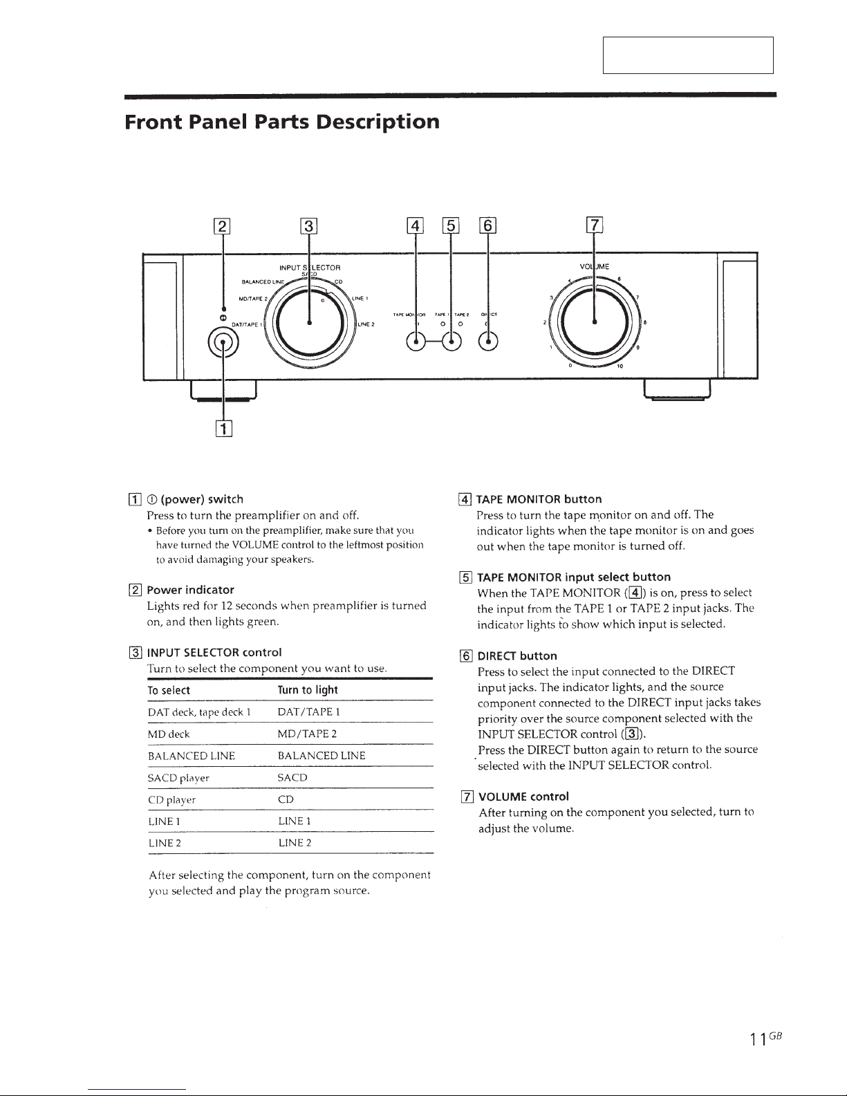
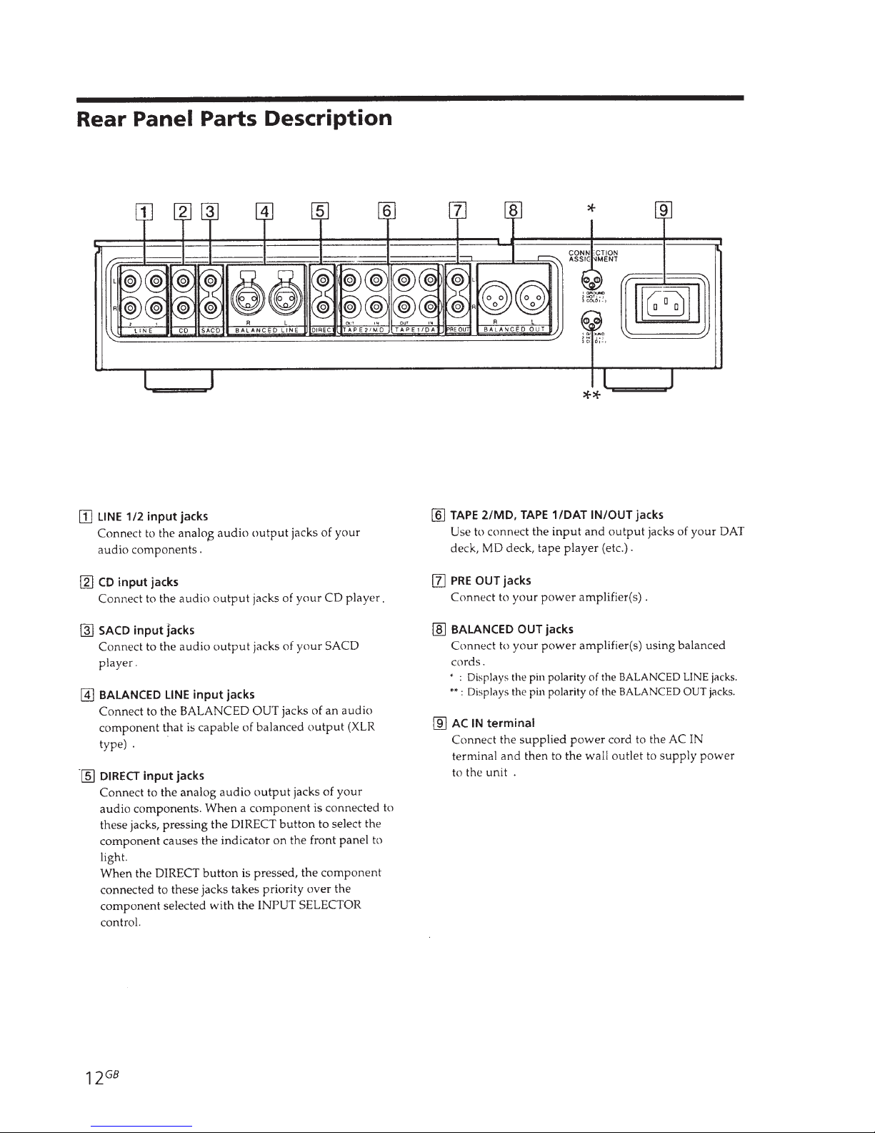
1
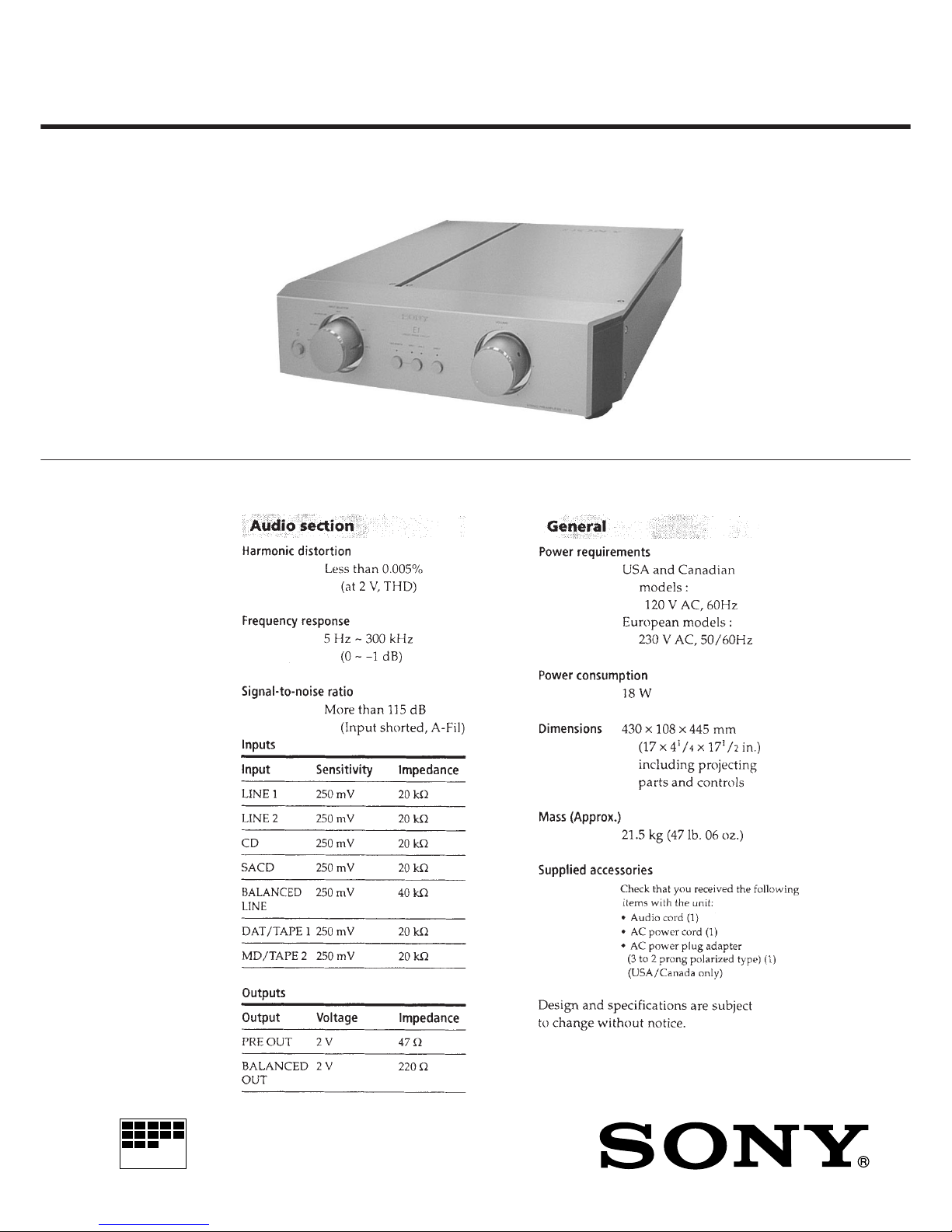
TA-E1
SPECIFICATIONS
STEREO PRE AMPLIFIER
SERVICE MANUAL
US Model
Canadian Model
AEP Model
UK Model
E Model
Australian Model
MICROFILM
2
TABLE OF CONTENTS
1. GENERAL ........................................................................... 3
2. ELECTRICAL ADJUSTMENT .................................... 5
3. DIAGRAMS
3-1. Circuit Boards Location ........................................................ 5
3-2. Schematic Diagram – Main Section (1/3) –..........................6
3-3. Schematic Diagram – Main Section (2/3) –..........................7
3-4. Schematic Diagram – Main Section (3/3) –..........................8
3-5. Printed Wiring Board – Main Section –................................ 9
3-6. Schematic Diagram – Power Section –............................... 10
3-7. Printed Wiring Board – Power Section –............................ 11
4. EXPLODED VIEWS
4-1. Top Plate and Back Panel Section....................................... 12
4-2. Front Panel Section ............................................................. 12
4-3. Bottom Plate Section .......................................................... 13
5. ELECTRICAL PARTS LIST ................................... 14
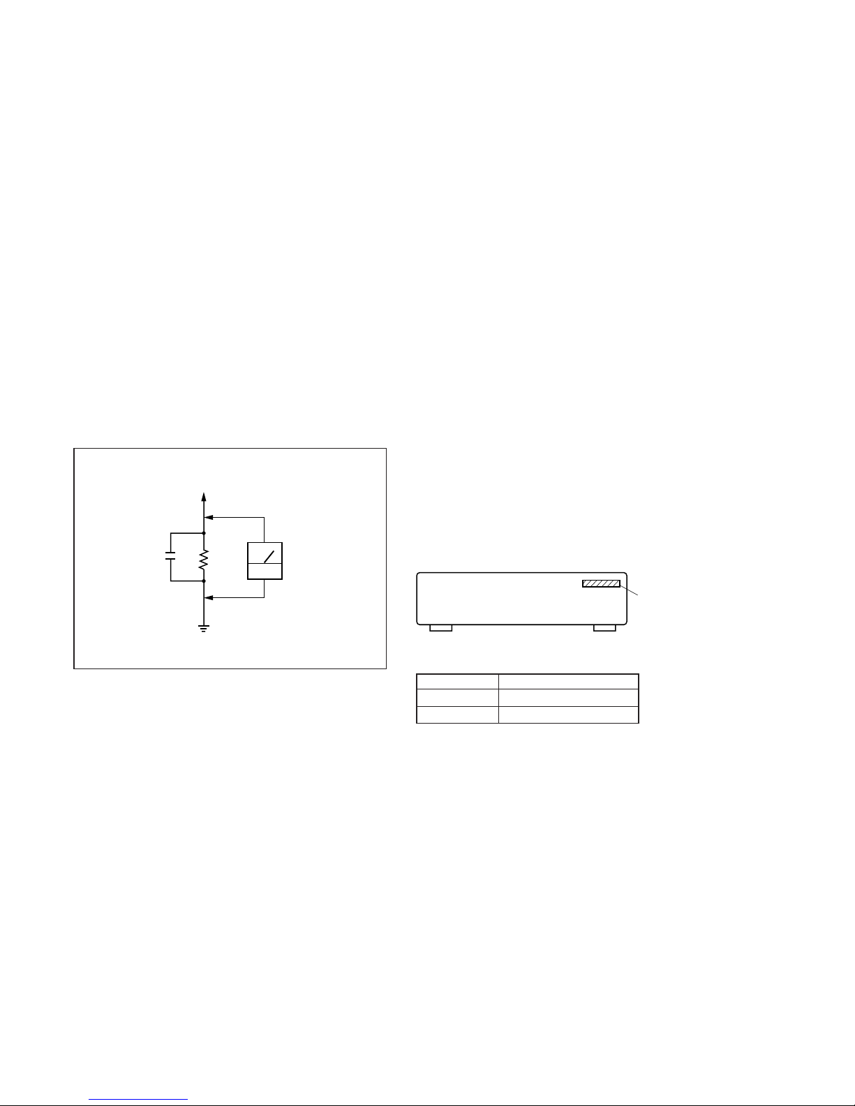
SAFETY CHECK-OUT
After correcting the original service problem, perform the following safety checks before releasing the set to the customer:
Check the antenna terminals, metal trim, “metallized” knobs, screws,
and all other exposed metal parts for AC leakage. Check leakage as
described below.
LEAKAGE
The AC leakage from any exposed metal part to earth Ground and
from all exposed metal parts to any exposed metal part having a
return to chassis, must not exceed 0.5 mA (500 microampers). Leakage current can be measured by any one of three methods.
1. A commercial leakage tester, such as the Simpson 229 or RCA
WT-540A. Follow the manufacturers’ instructions to use these
instruments.
2. A battery-operated AC milliammeter. The Data Precision 245
digital multimeter is suitable for this job.
3. Measuring the voltage drop across a resistor by means of a VOM
or battery-operated AC voltmeter . The “limit” indication is 0.75
V, so analog meters must have an accurate low-voltage scale.
The Simpson 250 and Sanwa SH-63Trd are examples of a passive VOM that is suitable. Nearly all battery operated digital
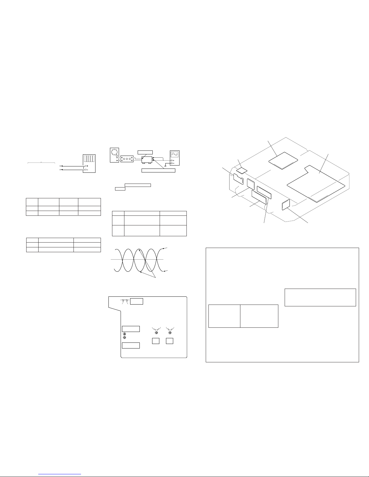
multimeters that have a 2V AC range are suitable. (See Fig. A)
Fig. A. Using an AC voltmeter to check AC leakage.
0.15µF
To Exposed Metal
Parts on Set
1.5k
Ω
AC
voltmeter
(0.75V)
Earth Ground
SAFETY-RELATED COMPONENT WARNING !!
COMPONENTS IDENTIFIED BY MARK ! OR DO TTED LINE
WITH MARK ! ON THE SCHEMATIC DIAGRAMS AND IN
THE PARTS LIST ARE CRITICAL TO SAFE OPERATION.
REPLACE THESE COMPONENTS WITH SONY PARTS
WHOSE PART NUMBERS APPEAR AS SHOWN IN THIS
MANUAL OR IN SUPPLEMENTS PUBLISHED BY SONY.
ATTENTION AU COMPOSANT AYANT RAPPORT
À LA SÉCURITÉ!!
LES COMPOSANTS IDENTIFIÉS P AR UNE MARQUE ! SUR
LES DIAGRAMMES SCHÉMATIQUES ET LA LISTE DES
PIÈCES SONT CRITIQUES POUR LA SÉCURITÉ DE
FONCTIONNEMENT. NE REMPLACER CES COMPOSANTS
QUE PAR DES PIÈCES SONY DONT LES NUMÉROS
SONT DONNÉS DANS CE MANUEL OU DANS LES
SUPPLÉMENTS PUBLIÉS PAR SONY.
MODEL IDENTIFICATION
— BACK PANEL —
PARTS No. MODEL
4-214-526-1π US , CND
4-214-526-2π AEP, UK, E, AUS
Parts No.
• Abbreviation
CND : Canadian model
AUS : Australian model
3
SECTION 1
GENERAL
This section is extracted from
instruction manual.
4
TA-E1
55
SECTION 3
DIAGRAMS
3-1. CIRCUIT BOARDS LOCATION
SECTION 2
ELECTRICAL ADJUSTMENTS
IDLING ADJUSTMENT AND OFFSET VOLTAGE
CHECK
• Perform this adjustment after replacing CP103 and CP104.
• Perform this adjustment more than 10 minutes after supplying
the power.
Connection:
BALANCE OUTPUT LEVEL ADJUSTMENT
• Perform this adjustment when replacing CP102.
• Perform this adjustment after the idling adjustment
Connection:
MAIN board
SW L board
AC J board
LED A board
LED B board
SW P board
PS board
VOL board
THIS NOTE IS COMMON FOR PRINTED WIRING
BOARDS AND SCHEMATIC DIAGRAMS.
(In addition to this, the necessary note is printed
in each block.)
For schematic diagrams.
Note:
• All capacitors are in µF unless otherwise noted. pF: µµF
50 WV or less are not indicated except for electrolytics
and tantalums.
• All resistors are in Ω and 1/
4
W or less unless otherwise
specified.
• % : indicates tolerance.
• 2 : nonflammable resistor.
• 5 : fusible resistor.
• C : panel designation.
• S : B+ Line.
• T : B– Line.
• H : adjustment for repair.
• Voltages and waveforms are dc with respect to ground in
playback mode.
• Voltages are taken with a VOM (Input impedance 10 MΩ).
Voltage variations may be noted due to normal production tolerances.
• Signal path.
F : TUNER
Note:
The components identified by mark ! or dotted
line with mark ! are critical for safety.
Replace only with part
number specified.
Note:
Les composants identifiés par
une marque ! sont critiques
pour la sécurité.
Ne les remplacer que par une
piéce portant le numéro
spécifié.
For printed wiring boards.
Note:
• X : parts extracted from the component side.
•®: Through hole.
• b : Pattern from the side which enables seeing.
(The other layers' patterns are not indicated.)
Caution:
Pattern face side: Parts on the pattern face side seen from the
(Side B) pattern face are indicated.
Parts face side: Parts on the parts face side seen from the
(Side A) parts face are indicated.
Digital voltmeter
TP501 (L-CH), TP502 (R-CH)
TP503 (L-CH), TP504 (R-CH)
MAIN board
Procedure:
1. Connect the digital voltmeter as shown above.
2. Adjust RV501 (L-CH) and RV502 (R-CH) of the MAIN board
so that the digital voltmeter reads 50 mV ±5 mV. (Idling adjustment)
3. Measure the voltage of both terminals of R221 (L-CH) and R222
(R-CH) of the MAIN board, and check that the voltage is within
2 mV.
(Offset voltage check)
Measuring Adjusting Adjusting
Point Point Value
L-CH TP501 to TP503 RV501 50 mV ± 5 mV
R-CH TP502 to TP504 RV502 50 mV ± 5 mV
Measuring Point Specified Value
L-CH Both terminals of R221 Within 2 mV
R-CH Both terminals of R222 Within 2 mV
Procedure:
1. Connect as shown above.
2. Rotate the INPUT SELECTOR knob, and set the input source
to LINE 1 .
3. Set the input level so that the oscilloscope waveform level becomes approx 3 V.
4. Adjust RV401 (L-CH) and R V402 (R-CH) so that the two waveform levels on the oscilloscope become equal and their phases
are reversed.
BALANCED-OUT 2 3 pin
LINE1 input
Set
AF OSC
attenuator
Oscilloscope
Adjusting Value:
Adjusting Point Adjusting Value
L-CH Pin 2 (CH1) and RV401
Pin 3 (CH2) of CN203
R-CH Pin 2 (CH1) and RV401
Pin 3 (CH2) of CN203
Phases of waveforms of
Pins
2
and 3 should be reversed
Waveform of
Pin
2
(CH1)
Waveform of
Pin
3
(CH2)
Adjustment Location:
[MAIN board] (Component Side)
OFFSET
VOLTAGE
R222
R221
RV401
BALANCE OUT
LEVEL L CH
RV402
BALANCE OUT
LEVEL R CH
RV501
IDLE
L CH
TP503
RV502
IDLE
R CH
TP501 TP504 TP502
TA-E1
6
6
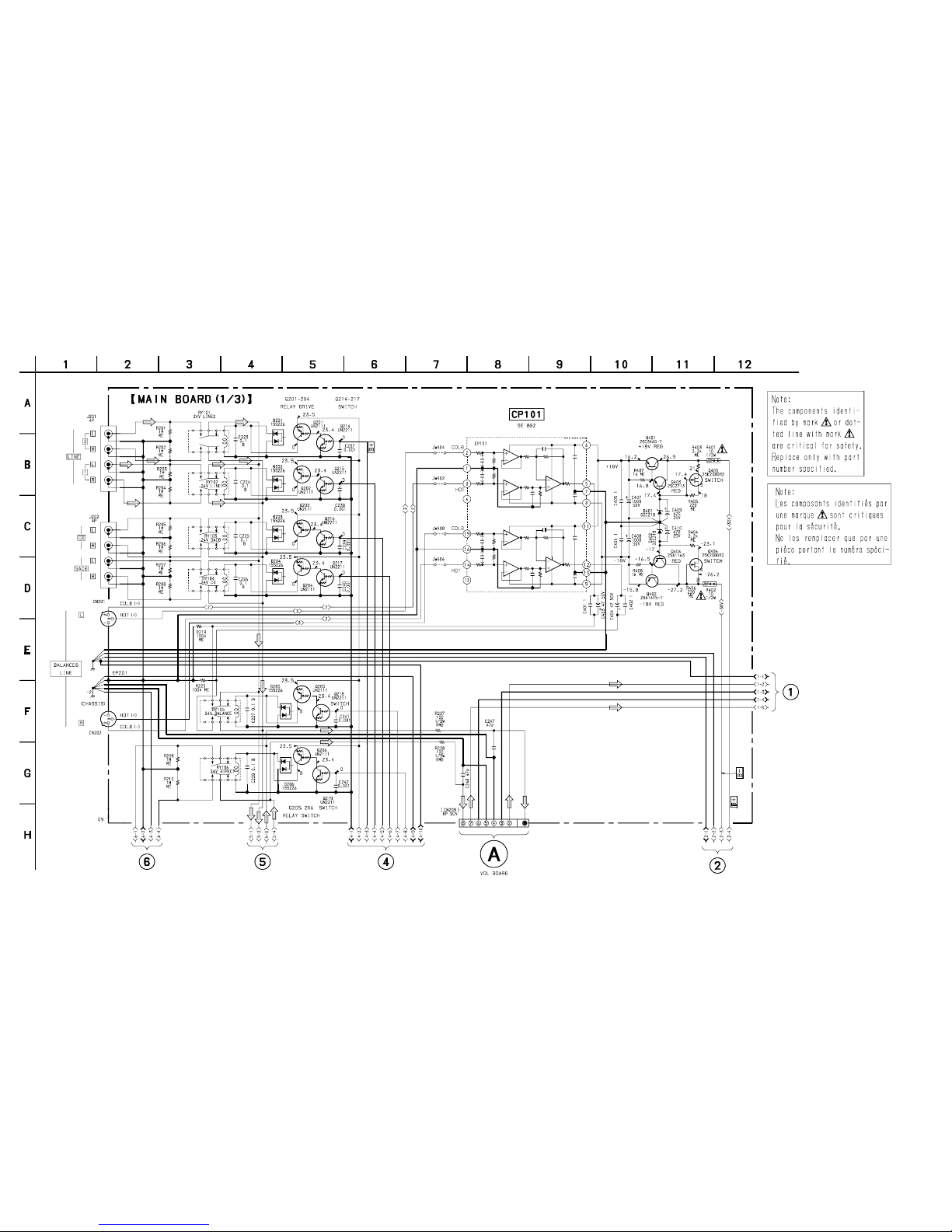
3-2. SCHEMATIC DIAGRAM – MAIN SECTION (1/3) –
• Refer to page 9 for Printed Wiring Board.
(Page 7) (Page 7) (Page 7)
(Page 7)
(Page 8)
(Page 10)

TA-E1
77
3-3. SCHEMATIC DIAGRAM – MAIN SECTION (2/3) –
• Refer to page 9 for Printed Wiring Board.
(Page 6) (Page 6) (Page 6) (Page 8)
(Page 6)
(Page 8)
(Page 10)(Page 10)(Page 10)

TA-E1
8
8
3-4. SCHEMATIC DIAGRAM – MAIN SECTION (3/3) –
(Page 6) (Page 7) (Page 7)

TA-E1
99
3-5. PRINTED WIRING BOARD – MAIN SECTION –
• Refer to page 5 for Circuit Boards Location.
Ref. No Location
D201 B-1
D202 B-1
D203 B-2
D204 B-3
D205 B-4
D206 B-5
D207 B-6
D208 B-8
D209 B-8
D210 B-7
D211 B-10
D212 B-10
D401 I-2
D402 I-2
D403 I-9
D404 I-9
D405 I-8
D406 I-8
D407 I-7
D408 I-7
D501 I-6
D502 I-5
D503 I-4
D504 I-4
D505 I-3
D506 I-4
Q201 B-1
Q202 B-2
Q203 B-3
Q204 B-3
Q205 B-5
Q206 B-6
Q207 B-6
Q208 B-8
Q209 B-7
Q210 B-7
Q211 B-7
Q212 B-10
Q214 B-1
Q215 B-2
Q216 B-3
Q217 B-4
Q218 B-5
Q219 B-6
Q220 B-7
Q221 B-8
Q222 B-7
Q223 B-7
Q224 B-10
Q225 B-11
Q401 I-2
Q402 I-2
Q403 I-2
Q404 I-2
Q405 I-3
Q406 I-2
Q407 I-10
Q408 I-9
Q409 I-9
Q410 I-9
Q411 I-10
Q412 I-9
Q501 F-5
Q502 F-3
Q503 I-8
Q504 I-7
Q505 I-8
Q506 I-7
Q507 I-8
Q508 I-7
Q509 I-6
Q510 I-5
Q511 I-6
Q512 I-5
Q513 I-6
Q514 I-5
Q515 I-4
Q516 I-3
Q517 I-4
Q518 I-3
Q519 I-4
Q520 I-4
• Semiconductor
Location
(Page 11)
(Page 11)
(Page 11)
(Page 11)
VOL
BOARD
SW L
BOARD
SW L
BOARD
PS
BOARD

TA-E1
10
10
3-6. SCHEMATIC DIAGRAM – POWER SECTION –
(Page 6)
(Page 7)
(Page 7)
(Page 7)

TA-E1
11 11
3-7. PRINTED WIRING BOARD – POWER SECTION –
• Refer to page 5 for Circuit Boards Location.
(Page 9)
MAIN BOARD
(Page 9) (Page 9)
MAIN
BOARD
MAIN
BOARD
(Page 9)
MAIN
BOARD
F H 2F H 1
Ref. No Location
D701 C-1
D702 C-1
D703 B-4
D704 B-3
D705 B-3
D706 B-2
D707 C-5
D708 A-5
D709 A-5
D710 D-5
IC701 C-5
Q701 A-4
Q702 A-2
Q703 A-4
Q704 A-2
Q705 C-4
Q706 B-3
Q707 B-5
Q708 A-5
Q709 A-5
Q710 B-5
• Semiconductor
Location

12 12
Ref. No. Part No. Description Remark Ref. No. Part No. Description Remark
SECTION 4
EXPLODED VIEWS
Ref. No. Part No. Description Remark
Ref. No. Part No. Description Remark
NOTE:
• -XX, -X mean standardized parts, so they may have
some difference from the original one.
• Items marked “*” are not stocked since they are
seldom required for routine service. Some delay
should be anticipated when ordering these items.
• The mechanical parts with no reference number in
the exploded views are not supplied.
• Hardware (# mark) list and accessories and packing materials are given in the last of this parts list.
• Abbreviation
CND : Canadian model
The components identified by
mark ! or dotted line with mark
! are critical for safety.
Replace only with part number
specified.
Les composants identifiés par une
marque ! sont critiques pour la
sécurité.
Ne les remplacer que par une
piéce portant le numéro spécifié.
7 4-911-049-21 SCREW (3X8)
8 4-970-124-11 CUSHION (F50180S)
9 3-703-685-41 SCREW (A+BV 3X8)
10 X-4951-584-1 FOOT ASSY
11 4-974-510-01 SCREW (+BV 3X8 CU)
12 X-4951-020-1 PLATE (L) ASSY,ORNAMENTAL SIDE
13 X-4951-021-1 PLATE (R) ASSY,ORNAMENTAL SIDE
* 14 3-703-044-26 LABEL, CAUTION (US,CND)
1 4-214-524-01 PLATE (L), TOP
2 4-214-525-01 PLATE (R), TOP
3 4-988-742-11 SCREW (M3X8), HEXAGON SOCKET
4 4-214-526-13 PANEL, BACK (US,CND)
4 4-214-526-22 PANEL, BACK (EXCEPT US,CND)
* 5 3-910-074-01 BOLT (M3)
6 1-580-375-41 INLET 3P
60 X-4950-854-1 BUTTON ASSY, POWER
61 1-673-514-11 AC J BOARD
62 1-673-518-11 SW P BOARD
63 1-673-513-11 SW L BOARD
64 1-673-517-11 LED B BOARD
65 1-673-519-11 VOL BOARD
66 3-655-653-21 BAND (TAITON), BINDING
67 4-221-587-01 TUBE, LIGHT INTERCEPTION
51 4-214-521-01 PANEL, FRONT
* 52 4-986-734-01 LENS, LED
53 4-214-533-01 RETAINER, LENS
54 4-214-620-01 SUPPORT (C)
55 4-214-532-01 KNOB (VOL)
56 4-214-545-01 KNOB (SELECTER)
57 X-4950-674-1 BUTTON ASSY
58 4-214-535-01 WINDOW, MIRROR
59 1-673-516-11 LED A BOARD (EXCEPT US,CND)
4-2. FRONT PANEL SECTION
4-1. TOP PLATE AND BACK PANEL SECTION
12
13
not supplied
not supplied
not supplied
not supplied
not supplied
not supplied
not supplied
not supplied
not supplied
not supplied
not supplied
not supplied
not supplied
FRONT PANEL
#1
#1
#1
#1
#1
#1
#1
#1
#1
#2
#2
#2
#2
#3
#3
#3
1
2
3
3
3
3
3
3
4
5
5
6
7
8
8
8
8
9
9
10
10
10
10
11
11
11
11
14
#5
#5
#5
#5
#4
#7
#7
#7
#7
#4
#4
#10
#10
#4
not supplied
not supplied
not supplied
not supplied
Supplied
with S601
Supplied
with RV301
not supplied
51
52
52
53
53
54
55
56
57
58
59
58
60
61
62
63
64
65
66
67

13
Ref. No. Part No. Description Remark Ref. No. Part No. Description Remark
Les composants identifiés par une
marque ! sont critiques pour la sécurité.
Ne les remplacer que par une piéce
portant le numéro spécifié.
The components identified by mark !
or dotted line with mark ! are critical
for safety.
Replace only with part number specified.
109 4-967-960-01 SCREW (4X8)
* 110 4-931-964-01 SCREW (M4X6)
* 111 1-641-950-11 PC BOARD, BOTTOM LID
112 A-4426-205-A MAIN BOARD, COMPLETE (US,CND)
112 A-4426-208-A MAIN BOARD, COMPLETE (EXCEPT US,CND)
113 4-974-510-01 SCREW (+BV 3X8 CU)
! T1 1-433-981-11 TRANSFORMER, POWER (EXCEPT US,CND)
! T1 1-433-982-11 TRANSFORMER, POWER (US,CND)
101 4-219-714-01 PLATE (A), BOTTOM
102 4-214-527-01 PLATE, BOTTOM
103 4-219-712-01 PLATE (A), TOP
104 4-219-713-01 PLATE (B), TOP
105 A-4426-207-A PS BOARD, COMPLETE (US,CND)
105 A-4426-210-A PS BOARD, COMPLETE (EXCEPT US,CND)
* 106 4-941-237-01 HEAT SINK
107 4-902-345-01 HEAT SINK
108 2-259-121-01 SCREW, TR
4-3. BOTTOM PLATE SECTION
#6
#6
#7
#7
#8
#7
#7
#9
#7 (EXCEPT,
US, CND)
#8 (US, CND)
#7 (EXCEPT,
US, CND)
#8 (US, CND)
#7
#3
101
102
103
104
109
109
109 109
109
105
106
108
108
108
110
111
111
107
113
113
113
not supplied
not supplied
not supplied
not supplied
not supplied
not supplied
T1
not supplied
not supplied
not supplied
112
(US, CND)

14
SECTION 5
ELECTRICAL PARTS LIST
AC J
Note:
Ref. No. Part No. Description Remark Ref. No. Part No. Description Remark
• SEMICONDUCTORS
In each case, u: µ , for example:
uA...: µ A..., uPA...: µ PA..., uPB...: µ PB...,
uPC...: µ PC..., uPD...: µ PD...
• CAPACITORS
uF : µ F
• COILS
uH : µ H
• Abbreviation
CND : Canadian model
• Due to standardization, replacements in the parts list
may be different from the parts specified in the
diagrams or the components used on the set.
• -XX, -X mean standardized parts, so they may have
some difference from the original one.
• Items marked “*” are not stocked since they are
seldom required for routine service. Some delay
should be anticipated when ordering these items.
• RESISTORS
All resistors are in ohms
METAL: Metal-film resistor
METAL OXIDE: Metal Oxide-film resistor
F : nonflammable
When indicating parts by reference
number, please include the board
name.
The components identified by
mark ! or dotted line with mark
! are critical for safety.
Replace only with part number
specified.
Les composants identifiés par une
marque ! sont critiques pour la
sécurité.
Ne les remplacer que par une
piéce portant le numéro spécifié.
1-673-514-11 AC J BOARD
*********
1-533-798-11 HOLDER, FUSE
< CAPACITOR >
! C901 1-113-920-11 CERAMIC 0.0022uF 20% 250V
< CONNECTOR >
CN902 1-564-321-00 PIN, CONNECTOR 2P
< FUSE >
! F901 1-532-463-51 FUSE (1A/250)(EXCEPT US,CND)
! F901 1-532-742-11 FUSE, GLASS TUBE (1.6A/125V)(US,CND)
< SWITCH >
! S901 1-771-187-11 SWITCH, AC POWER (U)
**************************************************************
1-673-516-11 LED A BOARD
**********
< CAPACITOR >
C801 1-115-339-11 CERAMIC CHIP 0.1uF 10% 50V
C802 1-115-339-11 CERAMIC CHIP 0.1uF 10% 50V
< CONNECTOR >
CN801 1-691-765-11 PLUG (MICRO CONNECTOR) 3P
< DIODE >
D801 8-719-313-40 DIODE SML1516W (U)
**************************************************************
1-673-517-11 LED B BOARD
**********
< CAPACITOR >
C605 1-163-021-91 CERAMIC CHIP 0.01uF 10% 50V
C606 1-163-021-91 CERAMIC CHIP 0.01uF 10% 50V
C607 1-163-021-91 CERAMIC CHIP 0.01uF 10% 50V
C608 1-163-021-91 CERAMIC CHIP 0.01uF 10% 50V
< DIODE >
D601 8-719-046-38 DIODE SEL5821A-TH8F (TAPE MONITOR)
D602 8-719-046-38 DIODE SEL5821A-TH8F (TAPE 1)
D603 8-719-046-38 DIODE SEL5821A-TH8F (TAPE 2)
D604 8-719-046-38 DIODE SEL5821A-TH8F (DIRECT)
**************************************************************
A-4426-205-A MAIN BOARD, COMPLETE (US,CND)
*********************
A-4426-208-A MAIN BOARD, COMPLETE (EXCEPT US,CND)
*********************
4-835-639-00 PLATE, GROUND
< CAPACITOR >
C223 1-115-339-11 CERAMIC CHIP 0.1uF 10% 50V
C224 1-115-339-11 CERAMIC CHIP 0.1uF 10% 50V
C225 1-115-339-11 CERAMIC CHIP 0.1uF 10% 50V
C226 1-115-339-11 CERAMIC CHIP 0.1uF 10% 50V
C227 1-115-339-11 CERAMIC CHIP 0.1uF 10% 50V
C228 1-115-339-11 CERAMIC CHIP 0.1uF 10% 50V
C229 1-115-339-11 CERAMIC CHIP 0.1uF 10% 50V
C230 1-115-339-11 CERAMIC CHIP 0.1uF 10% 50V
C231 1-115-339-11 CERAMIC CHIP 0.1uF 10% 50V
C232 1-115-339-11 CERAMIC CHIP 0.1uF 10% 50V
C233 1-115-339-11 CERAMIC CHIP 0.1uF 10% 50V
C234 1-115-339-11 CERAMIC CHIP 0.1uF 10% 50V
C237 1-163-009-11 CERAMIC CHIP 0.001uF 10% 50V
C238 1-163-009-11 CERAMIC CHIP 0.001uF 10% 50V
C239 1-163-009-11 CERAMIC CHIP 0.001uF 10% 50V
C240 1-163-009-11 CERAMIC CHIP 0.001uF 10% 50V
C241 1-163-009-11 CERAMIC CHIP 0.001uF 10% 50V
C242 1-163-009-11 CERAMIC CHIP 0.001uF 10% 50V
C243 1-163-009-11 CERAMIC CHIP 0.001uF 10% 50V
C244 1-163-009-11 CERAMIC CHIP 0.001uF 10% 50V
C245 1-163-009-11 CERAMIC CHIP 0.001uF 10% 50V
C246 1-163-009-11 CERAMIC CHIP 0.001uF 10% 50V
C247 1-125-845-21 FILM 47PF 10% 50V
C248 1-125-845-21 FILM 47PF 10% 50V
C249 1-163-009-11 CERAMIC CHIP 0.001uF 10% 50V
C250 1-163-009-11 CERAMIC CHIP 0.001uF 10% 50V
C401 1-110-512-51 FILM 1uF 10% 50V
C402 1-110-512-51 FILM 1uF 10% 50V
LED A
MAIN
LED B

15
Ref. No. Part No. Description Remark Ref. No. Part No. Description Remark
C403 1-128-200-11 ELECT 47uF 20% 50V
C404 1-128-200-11 ELECT 47uF 20% 50V
C405 1-110-512-51 FILM 1uF 10% 50V
C406 1-110-512-51 FILM 1uF 10% 50V
C407 1-128-972-11 ELECT 1000uF 20% 50V
C408 1-128-972-11 ELECT 1000uF 20% 50V
C409 1-128-973-11 ELECT 470uF 20% 25V
C410 1-128-973-11 ELECT 470uF 20% 25V
C411 1-128-200-11 ELECT 47uF 20% 50V
C412 1-128-200-11 ELECT 47uF 20% 50V
C413 1-128-200-11 ELECT 47uF 20% 50V
C414 1-128-200-11 ELECT 47uF 20% 50V
C419 1-110-512-51 FILM 1uF 10% 50V
C420 1-110-512-51 FILM 1uF 10% 50V
C421 1-128-972-11 ELECT 1000uF 20% 50V
C422 1-128-972-11 ELECT 1000uF 20% 50V
C423 1-128-973-11 ELECT 470uF 20% 25V
C424 1-128-973-11 ELECT 470uF 20% 25V
C501 1-125-850-21 FILM 220PF 5% 50V
C502 1-125-850-21 FILM 220PF 5% 50V
C503 1-110-512-51 FILM 1uF 10% 50V
C504 1-110-512-51 FILM 1uF 10% 50V
C505 1-128-971-11 ELECT 220uF 20% 50V
C506 1-128-971-11 ELECT 220uF 20% 50V
C507 1-128-971-11 ELECT 220uF 20% 50V
C508 1-128-971-11 ELECT 220uF 20% 50V
C509 1-128-973-11 ELECT 470uF 20% 25V
C510 1-128-973-11 ELECT 470uF 20% 25V
C511 1-128-972-11 ELECT 1000uF 20% 50V
C512 1-128-972-11 ELECT 1000uF 20% 50V
C513 1-110-512-51 FILM 1uF 10% 50V
C514 1-110-512-51 FILM 1uF 10% 50V
C515 1-128-973-11 ELECT 470uF 20% 25V
C516 1-128-973-11 ELECT 470uF 20% 25V
C517 1-126-017-11 ELECT 6800uF 20% 16V
C518 1-126-017-11 ELECT 6800uF 20% 16V
C519 1-110-512-51 FILM 1uF 10% 50V
C520 1-110-512-51 FILM 1uF 10% 50V
C521 1-128-973-11 ELECT 470uF 20% 25V
C522 1-128-973-11 ELECT 470uF 20% 25V
C523 1-128-972-11 ELECT 1000uF 20% 50V
C524 1-128-972-11 ELECT 1000uF 20% 50V
C525 1-110-512-51 FILM 1uF 10% 50V
C526 1-110-512-51 FILM 1uF 10% 50V
< CONNECTOR >
CN201 1-766-803-11 CONNECTOR (CANON)
CN202 1-766-803-11 CONNECTOR (CANON)
CN203 1-785-548-11 CONNECTOR (RECEPTACLE)
CN204 1-785-548-11 CONNECTOR (RECEPTACLE)
CN205 1-691-768-11 PLUG (MICRO CONNECTOR) 6P
CN206 1-691-769-11 PLUG (MICRO CONNECTOR) 7P
* CN207 1-564-241-11 PIN, CONNECTOR (B4P-VH) 4P
< COMPOSITION CIRCUIT BLOCK >
CP101 1-233-250-11 ENCAPSULATED COMPONENT
CP102 1-418-106-11 AMPLIFIER UNIT
CP103 1-418-107-11 AMPLIFIER UNIT
CP104 1-418-107-11 AMPLIFIER UNIT
< DIODE >
D201 8-719-800-76 DIODE 1SS226
D202 8-719-800-76 DIODE 1SS226
D203 8-719-800-76 DIODE 1SS226
D204 8-719-800-76 DIODE 1SS226
D205 8-719-800-76 DIODE 1SS226
D206 8-719-800-76 DIODE 1SS226
D207 8-719-800-76 DIODE 1SS226
D208 8-719-800-76 DIODE 1SS226
D209 8-719-800-76 DIODE 1SS226
D210 8-719-800-76 DIODE 1SS226
D211 8-719-800-76 DIODE 1SS226
D212 8-719-800-76 DIODE 1SS226
D401 8-719-025-51 DIODE 02CZ18-TE85L
D402 8-719-025-51 DIODE 02CZ18-TE85L
D403 8-719-025-51 DIODE 02CZ18-TE85L
D404 8-719-025-51 DIODE 02CZ18-TE85L
D405 8-719-025-47 DIODE 02CZ12-TE85L
D406 8-719-025-47 DIODE 02CZ12-TE85L
D407 8-719-025-47 DIODE 02CZ12-TE85L
D408 8-719-025-47 DIODE 02CZ12-TE85L
D501 8-719-025-51 DIODE 02CZ18-TE85L
D502 8-719-025-51 DIODE 02CZ18-TE85L
D503 8-719-025-47 DIODE 02CZ12-TE85L
D504 8-719-025-47 DIODE 02CZ12-TE85L
D505 8-719-025-47 DIODE 02CZ12-TE85L
D506 8-719-025-47 DIODE 02CZ12-TE85L
< JACK >
J201 1-785-547-11 JACK, PIN (LINE 1, 2 L/R)
J202 1-785-547-11 JACK, PIN (CD, SACD L/R)
J203 1-785-547-11 JACK, PIN (DIRECT L/R, TAPE2/MD IN L/R)
J204 1-785-547-11 JACK, PIN
(TAPE2/MD OUT L/R, TAPE1/DAT IN L/R)
J205 1-785-547-11 JACK, PIN (TAPE1/DAT OUT L/R, PRE OUT L/R)
< BUS BAR >
* JWH201 1-569-135-11 BAR, BUS 4P
* JWH202 1-569-135-11 BAR, BUS 4P
* JWH203 1-691-275-11 BUS BAR
* JWH204 1-569-135-11 BAR, BUS 4P
* JWH205 1-569-135-11 BAR, BUS 4P
* JWH206 1-691-275-11 BUS BAR
< TRANSISTOR >
Q201 8-729-424-08 TRANSISTOR UN2111
Q202 8-729-424-08 TRANSISTOR UN2111
Q203 8-729-424-08 TRANSISTOR UN2111
Q204 8-729-424-08 TRANSISTOR UN2111
Q205 8-729-424-08 TRANSISTOR UN2111
Q206 8-729-424-08 TRANSISTOR UN2111
Q207 8-729-424-08 TRANSISTOR UN2111
Q208 8-729-424-08 TRANSISTOR UN2111
Q209 8-729-424-08 TRANSISTOR UN2111
Q210 8-729-424-08 TRANSISTOR UN2111
MAIN

16
Ref. No. Part No. Description Remark Ref. No. Part No. Description Remark
Les composants identifiés par une
marque ! sont critiques pour la sécurité.
Ne les remplacer que par une piéce
portant le numéro spécifié.
The components identified by mark !
or dotted line with mark ! are critical
for safety.
Replace only with part number specified.
Q211 8-729-424-08 TRANSISTOR UN2111
Q212 8-729-424-08 TRANSISTOR UN2111
Q214 8-729-421-22 TRANSISTOR UN2211
Q215 8-729-421-22 TRANSISTOR UN2211
Q216 8-729-421-22 TRANSISTOR UN2211
Q217 8-729-421-22 TRANSISTOR UN2211
Q218 8-729-421-22 TRANSISTOR UN2211
Q219 8-729-421-22 TRANSISTOR UN2211
Q220 8-729-421-22 TRANSISTOR UN2211
Q221 8-729-421-22 TRANSISTOR UN2211
Q222 8-729-421-22 TRANSISTOR UN2211
Q223 8-729-421-22 TRANSISTOR UN2211
Q224 8-729-421-22 TRANSISTOR UN2211
Q225 8-729-421-22 TRANSISTOR UN2211
Q401 8-729-047-96 TRANSISTOR 2SC3645-S
Q402 8-729-047-94 TRANSISTOR 2SA1415-S
Q403 8-729-271-31 TRANSISTOR 2SC2713-G
Q404 8-729-216-31 TRANSISTOR 2SA1163-G
Q405 8-729-232-69 TRANSISTOR 2SK208-GRT5LSONY-1
Q406 8-729-232-69 TRANSISTOR 2SK208-GRT5LSONY-1
Q407 8-729-047-96 TRANSISTOR 2SC3645-S
Q408 8-729-047-94 TRANSISTOR 2SA1415-S
Q409 8-729-271-31 TRANSISTOR 2SC2713-G
Q410 8-729-216-31 TRANSISTOR 2SA1163-G
Q411 8-729-232-69 TRANSISTOR 2SK208-GRT5LSONY-1
Q412 8-729-232-69 TRANSISTOR 2SK208-GRT5LSONY-1
Q501 8-729-271-31 TRANSISTOR 2SC2713-G
Q502 8-729-271-31 TRANSISTOR 2SC2713-G
Q503 8-729-047-96 TRANSISTOR 2SC3645-S
Q504 8-729-047-94 TRANSISTOR 2SA1415-S
Q505 8-729-271-31 TRANSISTOR 2SC2713-G
Q506 8-729-216-31 TRANSISTOR 2SA1163-G
Q507 8-729-232-69 TRANSISTOR 2SK208-GRT5LSONY-1
Q508 8-729-232-69 TRANSISTOR 2SK208-GRT5LSONY-1
Q509 8-729-047-96 TRANSISTOR 2SC3645-S
Q510 8-729-047-94 TRANSISTOR 2SA1415-S
Q511 8-729-271-31 TRANSISTOR 2SC2713-G
Q512 8-729-216-31 TRANSISTOR 2SA1163-G
Q513 8-729-232-69 TRANSISTOR 2SK208-GRT5LSONY-1
Q514 8-729-232-69 TRANSISTOR 2SK208-GRT5LSONY-1
Q515 8-729-232-69 TRANSISTOR 2SK208-GRT5LSONY-1
Q516 8-729-232-69 TRANSISTOR 2SK208-GRT5LSONY-1
Q517 8-729-047-96 TRANSISTOR 2SC3645-S
Q518 8-729-047-94 TRANSISTOR 2SA1415-S
Q519 8-729-271-31 TRANSISTOR 2SC2713-G
Q520 8-729-216-31 TRANSISTOR 2SA1163-G
< RESISTOR >
R201 1-260-032-11 CARBON MELF 1M 2% 1/8W
R202 1-260-032-11 CARBON MELF 1M 2% 1/8W
R203 1-260-032-11 CARBON MELF 1M 2% 1/8W
R204 1-260-032-11 CARBON MELF 1M 2% 1/8W
R205 1-260-032-11 CARBON MELF 1M 2% 1/8W
R206 1-260-032-11 CARBON MELF 1M 2% 1/8W
R207 1-260-032-11 CARBON MELF 1M 2% 1/8W
R208 1-260-032-11 CARBON MELF 1M 2% 1/8W
R209 1-260-032-11 CARBON MELF 1M 2% 1/8W
R210 1-260-032-11 CARBON MELF 1M 2% 1/8W
R211 1-260-032-11 CARBON MELF 1M 2% 1/8W
R212 1-260-032-11 CARBON MELF 1M 2% 1/8W
R213 1-260-032-11 CARBON MELF 1M 2% 1/8W
R214 1-260-032-11 CARBON MELF 1M 2% 1/8W
R215 1-260-032-11 CARBON MELF 1M 2% 1/8W
R216 1-260-032-11 CARBON MELF 1M 2% 1/8W
R217 1-260-032-11 CARBON MELF 1M 2% 1/8W
R218 1-260-032-11 CARBON MELF 1M 2% 1/8W
R219 1-260-020-11 CARBON MELF 100K 2% 1/8W
R220 1-260-020-11 CARBON MELF 100K 2% 1/8W
R221 1-260-032-11 CARBON MELF 1M 2% 1/8W
R222 1-260-032-11 CARBON MELF 1M 2% 1/8W
R223 1-260-032-11 CARBON MELF 1M 2% 1/8W
R224 1-260-032-11 CARBON MELF 1M 2% 1/8W
R225 1-260-032-11 CARBON MELF 1M 2% 1/8W
R226 1-260-032-11 CARBON MELF 1M 2% 1/8W
R227 1-249-186-11 CARBON 100 1% 1/3W
R228 1-249-186-11 CARBON 100 1% 1/3W
R229 1-259-644-11 CARBON 47 2% 1W
R230 1-259-644-11 CARBON 47 2% 1W
R231 1-259-531-11 CARBON 100 1% 1/2W
R232 1-259-531-11 CARBON 100 1% 1/2W
R233 1-249-186-11 CARBON 100 1% 1/3W
R234 1-249-186-11 CARBON 100 1% 1/3W
R235 1-259-995-11 CARBON MELF 1K 2% 1/8W
R236 1-259-995-11 CARBON MELF 1K 2% 1/8W
! R401 1-202-937-41 FUSIBLE 10 5% 1/2W
! R402 1-202-937-41 FUSIBLE 10 5% 1/2W
R403 1-259-999-11 CARBON MELF 2.2K 2% 1/8W
R404 1-259-999-11 CARBON MELF 2.2K 2% 1/8W
R405 1-259-987-11 CARBON MELF 220 2% 1/8W
R406 1-259-987-11 CARBON MELF 220 2% 1/8W
R407 1-259-995-11 CARBON MELF 1K 2% 1/8W
R408 1-259-995-11 CARBON MELF 1K 2% 1/8W
! R409 1-202-937-41 FUSIBLE 10 5% 1/2W
! R410 1-202-937-41 FUSIBLE 10 5% 1/2W
R411 1-259-999-11 CARBON MELF 2.2K 2% 1/8W
R412 1-259-999-11 CARBON MELF 2.2K 2% 1/8W
R413 1-259-987-11 CARBON MELF 220 2% 1/8W
R414 1-259-987-11 CARBON MELF 220 2% 1/8W
R415 1-259-995-11 CARBON MELF 1K 2% 1/8W
R416 1-259-995-11 CARBON MELF 1K 2% 1/8W
R501 1-259-668-61 CARBON 470 2% 1W
R502 1-259-668-61 CARBON 470 2% 1W
R503 1-259-535-61 CARBON 150 1% 1/2W
R504 1-259-535-61 CARBON 150 1% 1/2W
R505 1-259-668-61 CARBON 470 2% 1W
R506 1-259-668-61 CARBON 470 2% 1W
R507 1-260-002-11 CARBON MELF 3.3K 2% 1/8W
R508 1-259-991-11 CARBON MELF 470 2% 1/8W
R509 1-260-002-11 CARBON MELF 3.3K 2% 1/8W
R510 1-259-991-11 CARBON MELF 470 2% 1/8W
R511 1-259-999-11 CARBON MELF 2.2K 2% 1/8W
R512 1-259-999-11 CARBON MELF 2.2K 2% 1/8W
R513 1-259-987-11 CARBON MELF 220 2% 1/8W
R514 1-259-987-11 CARBON MELF 220 2% 1/8W
! R515 1-202-937-41 FUSIBLE 10 5% 1/2W
MAIN

17
Ref. No. Part No. Description Remark Ref. No. Part No. Description Remark
Les composants identifiés par une
marque ! sont critiques pour la sécurité.
Ne les remplacer que par une piéce
portant le numéro spécifié.
The components identified by mark !
or dotted line with mark ! are critical
for safety.
Replace only with part number specified.
! R516 1-202-937-41 FUSIBLE 10 5% 1/2W
! R517 1-202-937-41 FUSIBLE 10 5% 1/2W
! R518 1-202-937-41 FUSIBLE 10 5% 1/2W
R519 1-259-995-11 CARBON MELF 1K 2% 1/8W
R520 1-259-995-11 CARBON MELF 1K 2% 1/8W
R521 1-259-999-11 CARBON MELF 2.2K 2% 1/8W
R522 1-259-999-11 CARBON MELF 2.2K 2% 1/8W
R523 1-259-987-11 CARBON MELF 220 2% 1/8W
R524 1-259-987-11 CARBON MELF 220 2% 1/8W
R525 1-259-995-11 CARBON MELF 1K 2% 1/8W
R526 1-259-995-11 CARBON MELF 1K 2% 1/8W
! R527 1-202-937-41 FUSIBLE 10 5% 1/2W
! R528 1-202-937-41 FUSIBLE 10 5% 1/2W
R529 1-259-999-11 CARBON MELF 2.2K 2% 1/8W
R530 1-259-999-11 CARBON MELF 2.2K 2% 1/8W
R531 1-259-987-11 CARBON MELF 220 2% 1/8W
R532 1-259-987-11 CARBON MELF 220 2% 1/8W
R533 1-259-995-11 CARBON MELF 1K 2% 1/8W
R534 1-259-995-11 CARBON MELF 1K 2% 1/8W
R535 1-249-162-11 CARBON 10 1% 1/3W
R536 1-249-162-11 CARBON 10 1% 1/3W
< VARIABLE RESISTOR >
RV401 1-224-250-11 RES, ADJ, METAL GLAZE 2.2K
(BALANCED LEVEL LCH)
RV402 1-224-250-11 RES, ADJ, METAL GLAZE 2.2K
(BALANCED LEVEL RCH)
RV501 1-224-249-11 RES, ADJ, METAL GLAZE 1K (IDLER LCH)
RV502 1-224-249-11 RES, ADJ, METAL GLAZE 1K (IDLER RCH)
< RELAY >
RY101 1-755-062-11 RELAY
RY102 1-755-062-11 RELAY
RY103 1-755-062-11 RELAY
RY104 1-755-062-11 RELAY
RY105 1-755-062-11 RELAY
RY106 1-755-062-11 RELAY
RY107 1-755-062-11 RELAY
RY108 1-755-062-11 RELAY
RY109 1-755-062-11 RELAY
RY110 1-755-062-11 RELAY
RY111 1-755-062-11 RELAY
RY112 1-755-062-11 RELAY
RY113 1-755-062-11 RELAY
< TEST PIN >
* TP501 3-657-235-00 POINT, TEST
* TP502 3-657-235-00 POINT, TEST
* TP503 3-657-235-00 POINT, TEST
* TP504 3-657-235-00 POINT, TEST
**************************************************************
A-4426-207-A PS BOARD, COMPLETE (US,CND)
******************
A-4426-210-A PS BOARD, COMPLETE (EXCEPT US,CND)
*******************
< CAPACITOR >
C701 1-136-880-11 FILM 2.2uF 10% 160V
C702 1-128-998-11 ELECT 6800uF 20% 35V
C703 1-128-998-11 ELECT 6800uF 20% 35V
C706 1-128-200-11 ELECT 47uF 20% 50V
C707 1-128-200-11 ELECT 47uF 20% 50V
C708 1-117-775-31 FILM 0.1uF 10% 250V
C709 1-117-775-31 FILM 0.1uF 10% 250V
C710 1-127-982-11 ELECT 3900uF 20% 50V
C711 1-127-981-11 ELECT 3900uF 20% 50V
C716 1-130-955-11 FILM 0.01uF 2% 100V
C717 1-119-847-11 ELECT 2.2uF 20% 100V
C718 1-119-815-21 ELECT 2200uF 20% 35V
C719 1-126-025-11 ELECT 330uF 20% 25V
C720 1-119-804-21 ELECT 1000uF 20% 25V
< CONNECTOR >
CN702 1-564-510-11 PLUG (MICRO CONNECTOR) 6P
CN704 1-564-320-00 PIN, CONNECTOR (B2P-VH) 2P
* CN705 1-564-241-11 PIN, CONNECTOR (B4P-VH) 4P
< DIODE >
D701 8-719-200-39 DIODE C16P20F
D702 8-719-200-40 DIODE C16P20FR
D703 8-719-025-49 DIODE 02CZ15-TE85L
D704 8-719-025-49 DIODE 02CZ15-TE85L
D705 8-719-025-49 DIODE 02CZ15-TE85L
D706 8-719-025-49 DIODE 02CZ15-TE85L
D707 8-719-200-82 DIODE 11ES2
D708 8-719-025-47 DIODE 02CZ12-TE85L
D709 8-719-200-82 DIODE 11ES2
D710 8-719-070-64 DIODE RBV-602L
< IC >
IC701 8-759-605-03 IC M5F78M24L
< TRANSISTOR >
Q701 8-729-141-58 TRANSISTOR 2SC2275A-Q
Q702 8-729-141-10 TRANSISTOR 2SA985A-Q
Q703 8-729-271-31 TRANSISTOR 2SC2713-G
Q704 8-729-216-31 TRANSISTOR 2SA1163-G
Q705 8-729-232-69 TRANSISTOR 2SK208-GRT5LSONY-1
Q706 8-729-232-69 TRANSISTOR 2SK208-GRT5LSONY-1
Q707 8-729-271-31 TRANSISTOR 2SC2713-G
Q708 8-729-424-08 TRANSISTOR UN2111
Q709 8-729-424-08 TRANSISTOR UN2111
Q710 8-729-424-08 TRANSISTOR UN2111
< RESISTOR >
! R701 1-202-937-41 FUSIBLE 10 5% 1/2W
! R702 1-202-937-41 FUSIBLE 10 5% 1/2W
R703 1-259-999-11 CARBON MELF 2.2K 2% 1/8W
R704 1-259-999-11 CARBON MELF 2.2K 2% 1/8W
R705 1-259-987-11 CARBON MELF 220 2% 1/8W
R706 1-259-987-11 CARBON MELF 220 2% 1/8W
! R707 1-202-937-41 FUSIBLE 10 5% 1/2W
R708 1-259-995-11 CARBON MELF 1K 2% 1/8W
MAIN PS

18
Ref. No. Part No. Description Remark
Ref. No. Part No. Description Remark
R709 1-259-995-11 CARBON MELF 1K 2% 1/8W
! R710 1-202-937-41 FUSIBLE 10 5% 1/2W
! R711 1-202-937-41 FUSIBLE 10 5% 1/2W
R712 1-260-002-11 CARBON MELF 3.3K 2% 1/8W
R713 1-260-008-11 CARBON MELF 10K 2% 1/8W
R717 1-260-020-11 CARBON MELF 100K 2% 1/8W
R718 1-260-008-11 CARBON MELF 10K 2% 1/8W
R719 1-260-020-11 CARBON MELF 100K 2% 1/8W
R720 1-260-002-11 CARBON MELF 3.3K 2% 1/8W
R721 1-260-002-11 CARBON MELF 3.3K 2% 1/8W
1-673-519-11 VOL BIARD
**************************************************************
1-673-513-11 SW L BOARD
*********
< CAPACITOR >
C601 1-163-009-11 CERAMIC CHIP 0.001uF 10% 50V
C609 1-119-847-11 ELECT 2.2uF 20% 100V
< CONNECTOR >
CN601 1-691-769-11 PLUG (MICRO CONNECTOR) 7P
CN602 1-691-768-11 PLUG (MICRO CONNECTOR) 6P
< DIODE >
D605 8-719-800-76 DIODE 1SS226
< TRANSISTOR >
Q601 8-729-047-96 TRANSISTOR 2SC3645-S
< RESISTOR >
R602 1-260-008-11 CARBON MELF 10K 2% 1/8W
R608 1-259-978-11 CARBON MELF 39 2% 1/8W
R609 1-260-008-11 CARBON MELF 10K 2% 1/8W
< SWITCH >
S601 1-771-566-11 SWITCH, ROTARY (INPUT SELECTOR)
**************************************************************
1-673-518-11 SW P BOARD
*********
< CAPACITOR >
C602 1-163-009-11 CERAMIC CHIP 0.001uF 10% 50V
C603 1-163-009-11 CERAMIC CHIP 0.001uF 10% 50V
C604 1-163-009-11 CERAMIC CHIP 0.001uF 10% 50V
< CONNECTOR >
CN606 1-691-770-11 PLUG (MICRO CONNECTOR) 8P
CN607 1-691-768-11 PLUG (MICRO CONNECTOR) 6P
< DIODE >
D606 8-719-025-19 DIODE 02CZ2.2-TE85L
D607 8-719-043-82 DIODE 02CZ5.1Y-TE85L
< RESISTOR >
R601 1-260-008-11 CARBON MELF 10K 2% 1/8W
R603 1-260-008-11 CARBON MELF 10K 2% 1/8W
R604 1-260-008-11 CARBON MELF 10K 2% 1/8W
< SWITCH >
S602 1-771-567-11 SWITCH, PUSH (3 KEY)
(TAPE MONITOR, TAPE 1/2, DIRECT)
**************************************************************
1-673-519-11 VOL BOARD
*********
< CONNECTOR >
CN301 1-691-770-11 PLUG (MICRO CONNECTOR) 8P
< VARIABLE RESISTOR >
RV301 1-225-742-11 RES, VAR, CARBON 20K/20K
**************************************************************
MISCELLANEOUS
*************
6 1-580-375-41 INLET 3P
! T1 1-433-981-11 TRANSFORMER, POWER (EXCEPT US,CND)
! T1 1-433-982-11 TRANSFORMER, POWER (US,CND)
**************************************************************
ACCESSORIES & PACKING MATERIALS
*******************************
1-506-411-21 ADAPTOR, AC PLUG 3P-2P(US,CND)
1-551-631-22 CORD, POWER (EXCEPT US,CND)
1-551-812-11 CORD, POWER (US,CND)
1-558-271-11 CORD, CONNECTION (AUDIO, 108cm)
3-866-956-11 MANUAL, INSTRUCTION (ENGLISH,FRENCH)
3-866-956-21 MANUAL, INSTRUCTION (GERMAN,SPANISH,
DUTCH,SWEDISH,ITALIAN,PORTUGUESE)(EXCEPT US,CND)
**************************************************************
*************
HARDWARE LIST
*************
#1 7-621-775-10 SCREW +B 2.6X4
#2 7-682-566-04 SCREW +B 4X20
#2 7-682-567-09 SCREW +B 4X25 (US,CND)
#3 7-682-549-04 SCREW +B 3X10
#4 7-621-770-87 SCREW +B 2.6X5
#5 7-621-770-XX SCREW +B 2.6X8
#6 7-682-571-09 +B 4X45 (EXCEPT US,CND)
#7 7-685-871-09 SCREW +BVTT 3X6 (S)
#8 7-682-550-09 SCREW +B 3X12
#9 7-682-962-01 +PSW 4X10
#10 7-683-255-58 SET SCREW 5X6 HEXAGON SOCKET
Les composants identifiés par une
marque ! sont critiques pour la sécurité.
Ne les remplacer que par une piéce
portant le numéro spécifié.
The components identified by mark !
or dotted line with mark ! are critical
for safety.
Replace only with part number specified.
SW LPS
SW P VOL
Sony Corporation
Home Audio Company
9-928-912-11
99G0989-1
Printed in Japan © 1999. 7
Published by Quality Assurance Dept.
TA-E1
 Loading...