

Sony STRLV-500 Service manual
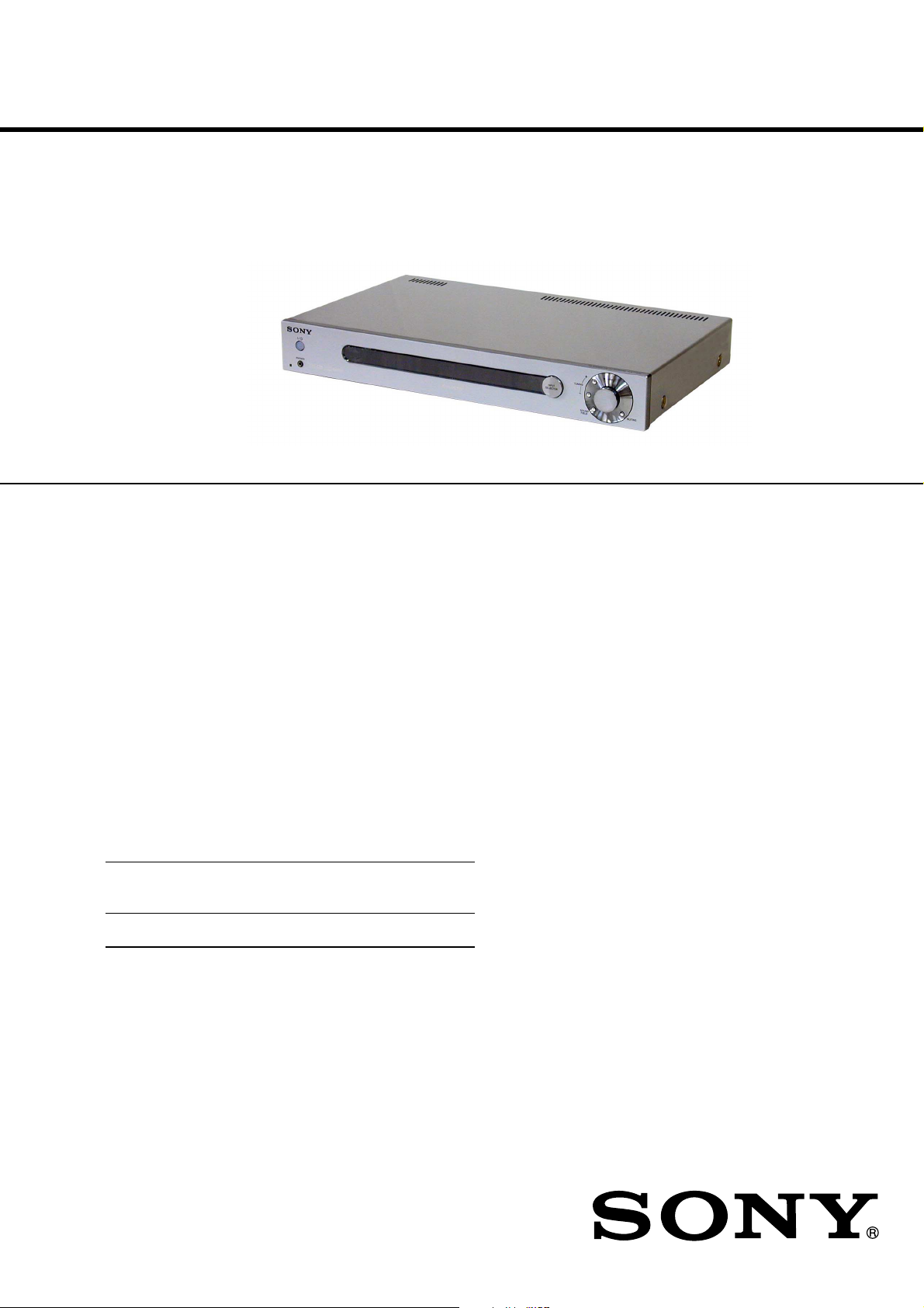
STR-LV500
SERVICE MANUAL
Ver 1.1 2004. 03
Manufactured under license from Dolby Laboratories.
“Dolby”, “Pro Logic” and the double-D symbol are
trademarks of Dolby Laboratories.
SPECIFICATIONS
Amplifier section
POWER OUTPUT
Rated Power Output at Stereo Mode
(8 ohms 1 kHz, DIN) 50 W + 50 W
Reference Power Output
(4 ohms 1 kHz, DIN) FRONT1): 75 W + 75 W
CENTER1): 75 W
SURROUND1): 75 W + 75 W
1) Depending on the sound field settings and the source, there may be
no sound output.
Frequency response 20 Hz – 20 kHz
Inputs (Analog) Sensitivity: 500 mV
Impedance: 50 kilohms
S/N2): 84 dB
(A, 500 mV3))
2) INPUT SHORT.
3) Weighted network, input level.
Inputs (Digital)
DVD (Coaxial) Impedance: 75 ohms
S/N: 90 dB
(A, 20 kHz LPF)
DVD, TV/SAT, S/N: 90 dB
HDD/MD (Optical) (A, 20 kHz LPF)
Sampling frequency
COAX, OPT 96 kHz
Outputs
LINE (sub woofer) Voltage: 2 V
Impedance: 1 kilohms
AEP Model
UK Model
FM tuner section
Tuning range 87.5 - 108.0 MHz
Antenna terminals 75 ohms, unbalanced
Intermediate frequency 10.7 MHz
Sensitivity
Mono: 18.3 dBf, 2.2 µV/75 ohms
Stereo: 38.3 dBf, 22.5 µV/75 ohms
Useable sensitivity 11.2 dBf, 1 µV/75 ohms
S/N
Mono: 76 dB
Stereo: 70 dB
Harmonic distortion at 1 kHz
Mono: 0.3%
Stereo: 0.5%
Separation 45 dB at 1 kHz
Frequency response 30 Hz – 15 kHz, +0.5/–2 dB
Selectivity 60 dB at 400 kHz
– Continued on next page –
9-877-452-02
2004C02-1
© 2004.03
FM STEREO
FM-AM RECEIVER
Sony Corporation
Home Audio Company
Published by Sony Engineering Corporation

STR-LV500
AM tuner section
Tuning range 531 – 1,602 kHz
Antenna Loop antenna
Intermediate frequency 450 kHz
Usable sensitivity 50 dB/m (at 999 kHz)
S/N 54 dB (at 50 mV/m)
Harmonic distortion 0.5% (50 mV/m, 400 Hz)
Selectivity
At 9 kHz: 35 dB
General
Power requirements 230 V AC, 50/60 Hz
Power consumption 95 W
Power consumption (during standby mode)
0.7 W
Dimensions 430 x 65 x 288 mm
including projecting parts and controls
Mass (Approx.) 2.7 kg
Supplied accessories
FM wire antenna (1)
AM loop antenna (1)
Remote commander (1)
R6 (size-AA) batteries (2)
Speaker plug (5)
Wrench (1)
Design and specifications are subject to change without notice.
TABLE OF CONTENTS
Specifications ............................................................................ 1
1. GENERAL ...................................................................... 3
2. SERVICING NOTES................................................... 4
3. TEST MODE ................................................................. 7
4. DIAGRAMS
4-1. IC Pin Function Descriptions ..................................9
4-2. Block Diagrams – Tuner/DSP Section – ............... 14
Block Diagrams – Display/Power Section – ......... 15
4-3. Printed Wiring Boards
– Digital Section (Side A)– ................................... 16
Printed Wiring Boards
– Digital Section (Side B)– ................................... 17
4-4. Schematic Diagram – Digital Section (1/3)– ........ 18
4-5. Schematic Diagram – Digital Section (2/3)– ........ 19
4-6. Schematic Diagram – Digital Section (3/3)– ........ 20
4-7. Schematic Diagram – Power Section– .................. 21
4-8. Printed Wiring Boards
– Power Section (Side A)– .................................... 22
Printed Wiring Boards
– Power Section (Side B)– .................................... 23
4-9. Printed Wiring Boards
– Amp Section (Side A)– ....................................... 24
Printed Wiring Boards
– Amp Section (Side B)–....................................... 25
3-10. Schematic Diagram – Amp Section (1/2)– ........... 26
3-11. Schematic Diagram – Amp Section (2/2)– ........... 27
3-12. Printed Wiring Boards – Display Section– ........... 28
3-13. Schematic Diagram – Display Section– ............... 29
3-14. IC Block Diagrams ................................................ 30
Unleaded solder
Boards requiring use of unleaded solder are printed with the leadfree mark (LF) indicating the solder contains no lead.
(Caution: Some printed circuit boards may not come printed with
the lead free mark due to their particular size.)
: LEAD FREE MARK
Unleaded solder has the following characteristics.
• Unleaded solder melts at a temperature about 40°C higher than
ordinary solder.
Ordinary soldering irons can be used but the iron tip has to be
applied to the solder joint for a slightly longer time.
Soldering irons using a temperature regulator should be set to
about 350°C.
Caution: The printed pattern (copper foil) may peel away if the
heated tip is applied for too long, so be careful!
• Strong viscosity
Unleaded solder is more viscous (sticky, less prone to flow) than
ordinary solder so use caution not to let solder bridges occur
such as on IC pins, etc.
• Usable with ordinary solder
It is best to use only unleaded solder but unleaded solder may
also be added to ordinary solder.
Notes on chip component replacement
• Never reuse a disconnected chip component.
• Notice that the minus side of a tantalum capacitor may be damaged by heat.
5. EXPLODED VIEWS
5-1. Front Panel Section ................................................. 31
5-2. Cabinet Section ........................................................ 32
6. ELECTRICAL PARTS LIST ....................................33
SAFETY-RELATED COMPONENT WARNING!!
COMPONENTS IDENTIFIED BY MARK 0 OR DOTTED LINE
WITH MARK 0 ON THE SCHEMATIC DIAGRAMS AND IN THE
PARTS LIST ARE CRITICAL TO SAFE OPERATION. REPLACE
THESE COMPONENTS WITH SONY PARTS WHOSE PART NUMBERS APPEAR AS SHOWN IN THIS MANUAL OR IN SUPPLEMENTS PUBLISHED BY SONY.
2
SECTION 1
GENERAL
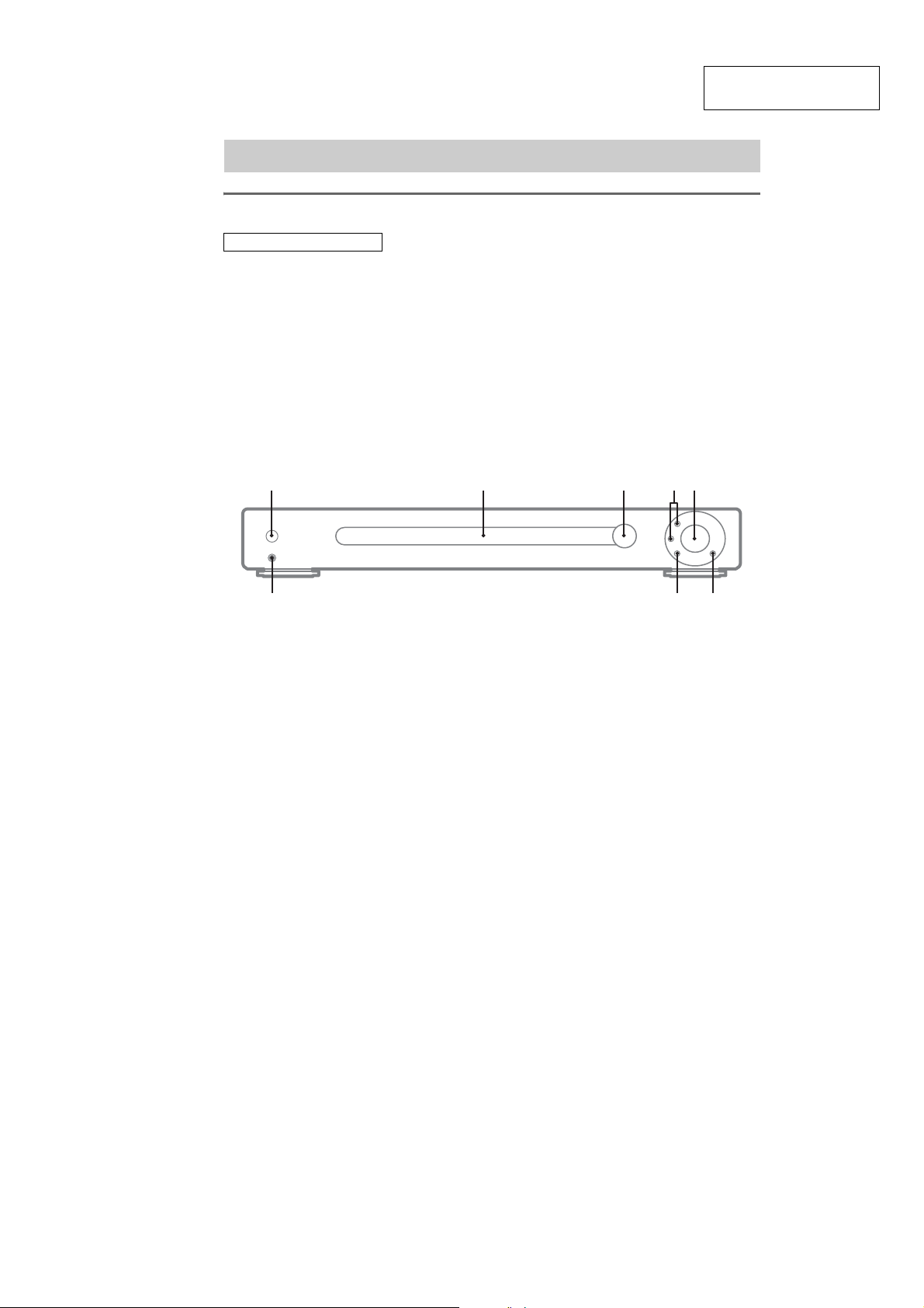
List of button locations and reference pages
Main unit
ALPHABETICAL ORDER
Display 2
INPUT SELECTOR 3
MUTING 6
PHONES jack 8
PRESET TUNING +/– 4
SOUND FIELD 7
VOLUME 5
?/1 (power) 1
1 2 354
STR-LV500
This section is extracted
from instruction manual.
8
67
3
STR-LV500
t
SERVICE POSITION
• POWER BOARD
Power board
SECTION 2
SERVICIN NOTE
1
Remove five screws
(+BVTP 3x8)
2
Isolation shee
4
s
s
s
• DIGITAL, DIG-IN, VIDEO BOARD
6
Dig-In board
4
Video board
2
Tuner unit
5
Five screws
(+BVTP 3x8)
3
Three screw
(+BVTP 3x8)
7
Three screw
(+BVTP 3x8)
1
Three screw
(+BVTP 3x8)
STR-LV500
Digital board
9
Digital board
Dig-In board
0
Video board
8
(+BVTP 3x8)
Isolation sheet
Four screws
5
STR-LV500
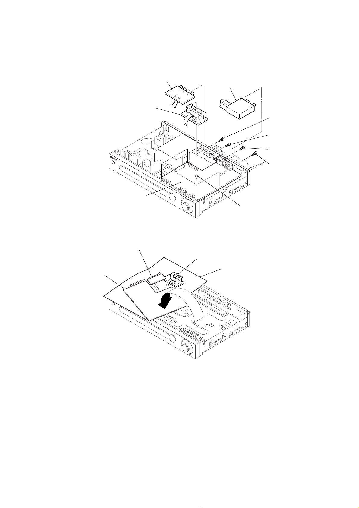
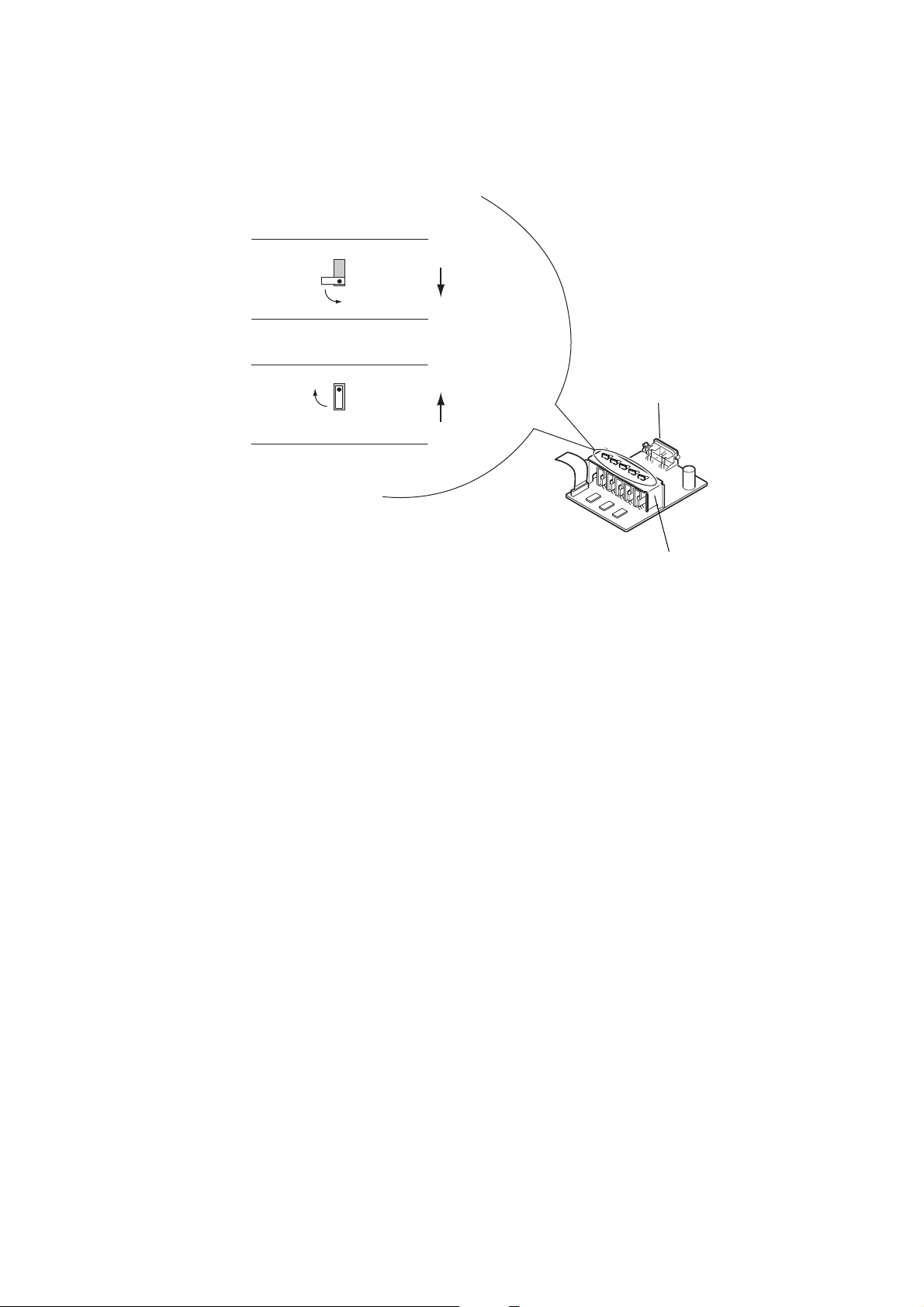
• AMP BOARD
• On Removal
1
Bend claws 90 degree
counterclokwise.
• On Attaching
2
Bend claws 90 degree
clokwise.
2
Slide down
the heat sink.
1
Slide up
the heat sink.
AMP board
Heat sink.
6
SECTION 3
TEST MODE
STR-LV500
Ver 1.1
SOUND FIELD CLEAR MODE
* The preset sound field is cleared when this mode is activated.
Use this mode before returning the product to clients upon
completion of repair.
* Procedure:
By using the main unit, while depressing the SOUND FIELD
button, press the power
button to turn on the main power.
?/1
The message “S. F . CLR” appears and initialization is performed.
SPECIAL DUPLEX KEY ON MODE
*This operation for making possible the key duplex pressing of
remote controller.
*Procedure
By using main unit, while depressing the
button, press the power
button to turn on the main
?/1
PRESET TUNNING -
power.
FACTORY PRESET MODE
* All preset contents are reset to the default setting.
* Procedure:
When the set is SPECIAL DUPLEX KEY ON mode, by using
remote controller, press ENTER button three times, then press
the MAIN MENU button one time, and then press the A.F.D.
button one time.
The message “FACTORY” appears and switch off the set.
Press the power
button again, and the present contents are
?/1
reset to the default values.
ALL CLEAR MODE
* The all preset value is cleared when this mode is activated.
* Procedure :
When the set is SPECIAL DUPLEX KEY ON mode, by using
remote controller, press ENTER button three times, then press
the MAIN MENU button one time, and then press the b but-
ton one time. The message “CLEARED” appears and clear all
preset value.
FLUORESCENT INDICATOR TUBE TEST MODE
* All fluorescent segments are tested. When this test is activated,
all segments turn on at the same time, then each segment turns
on one after another.
* Procedure:
When the set is SPECIAL DUPLEX KEY ON mode, by using
remote controller, press ENTER button three times, then press
the MAIN MENU button one time, and then press the V but-
ton one time.
All segments turn on.
D
D
SP SP A SP B
L
C R
SW
L F E
SL SRSSB
D
DIGITAL EX PRO LOGIC II DTS-ES
OPT COAX MULTI CH IN 12
D
D.RANGE
NEO : 6 MPEG-2 AAC
dB
kHz
mft.
MHz
RDSMONOSTEREOEQ
MEMORY
SLEEP
KEY CHECK MODE
* Button check
* Procedure:
When the set is SPECIAL DUPLEX KEY ON mode, by using
remote controller, press ENTER button three times, then press
the MAIN MENU button one time, and then press the v but-
ton one time.
“REST XX” appears.
Every pressing of any button other than
counts down the
?/1
buttons. The buttons which are already counted once are not
counted again. When all buttons are pressed “REST 00” appears.
SWAP ALL MODE
* For test all channels working correctly with only L/R source
input.
* Procedure:
When the set is SPECIAL DUPLEX KEY ON mode, by using
remote controller, press ENTER button three times, then press
the MAIN MENU button one time, and then press the 2CH
button one time.
Set the SOUND FIELD to A.F.D AUTO.
"SWAP ALL" appear : L-CH input t Front L, Surround L,
center channel output.
R-CH input t Front R , Surround R , Sub W oofer channel output.
HISTORY MODE
* Display embedded information.
For check amplifier condition when protector happen, Input
source, Sound Field setting, Volume level, Tone setting and
Operation time .
* Procedure :
When the set is SPECIAL DUPLEX KEY ON mode, by using
remote controller, press ENTER button three times, then press
the MAIN MENU button one time, and then press the
VOLUME + button one time.
DSP TEST MODE
* DSP tests are performed.
* Procedure :
When the set is SPECIAL DUPLEX KEY ON mode, by using
the remote controller, press ENTER button three times, then
press the MAIN MENU button one time and then press the
MUTING button one time.
• Select the item by pressing Cursor button ( V or v ).
• Select the function by pressing Cursor button ( B or b ).
RELEASE THE TEST MODE
To release the test mode, turn off the main power.
SOFTWARE VERSION DISPLAY MODE
* The software version is displayed.
* Procedure:
When the set is SPECIAL DUPLEX KEY ON mode, by using
remote controller, press ENTER button three times, then press
the MAIN MENU button one time, and then press the B but-
ton one time. The model name, destination and the software version are displayed.
7
STR-LV500
Items
SWAP
DSP Version
DSP communication
Bass Management
Main Speaker cut off Freq.
LFE cut off Freq.
Co-ef. Read Address
Co-ef. Read Data
Co-ef. Write Address
Co-ef. Write Data
SRAM
Total operation time
Longest Power ON time
Output time less than
–50dB volume
Output time less than
–40dB volume
Output time less than
–30dB volume
Output time less than
–20dB volume
Output time less than
–10dB volume
Output time less than
0dB volume
Protector count value
Fuse open count value
EEPROM CONDITION
EEPROM READ
EEPROM Super Reset
DSP HALT MODE
Function
NORM
ALL
C SW
SLSR
–
–
–
–
–
–
–
–
–
OFF
ON
–
–
–
–
–
–
–
–
–
–
–
–
–
–
Description
Normal channel output
Left input t Front Left, Surround Left, Center channel output
Right input t Front Right, Surround Right, Sub Woofer channel output
Left input t Center channel output
Right input t Sub Woofer channel output
Left input t Surround Left channel output
Right input t Surround Right channel output
“DSPV XXX” is displayed. Three large charactors are the dsp version that
is being used.
When this item is selected the message will be displayed “ OK ” if the
checking is correct. “ ERROR ” will be displayed in a case of an error.
Not used for service
Not used for service
Not used for service
Not used for service
Not used for service
Not used for service
Not used for service
“ RAMC. OFF ” will be displayed in a case of no checking.
By pressing Cursor button the checking starts.
“ RAMC. PASS ” will be displayed if the checking is good.
“ RAMC. NG ” will be displayed if an error occurs.
TTL-XXXX xx is displayed.
LNG-XXXX xx is displayed.
V50-XXXX xx is displayed.
V40-XXXX xx is displayed.
V30-XXXX xx is displayed.
V20-XXXX xx is displayed.
V10-XXXX xx is displayed.
V00-XXXX xx is displayed.
PROTXXXX xx is displayed.
FUSEXXXX xx is displayed.
E- XXXX is displayed.
S RST t Super Reset : first time use EEPROM or test pattern
corrupted
FAIL t EEPROM read / write with microcom has problem
V CHG t Software version change
D CHG t Destination / model change
CLEAR t Back up data initialize
NORM t Normal AC on
E- XXX-XX is displayed.
First four hex code is EEPROM address (controlled by +/– button).
Last two hex code is EEPROM data.
S.RST- XXX is displayed.
When YES is selected, press Cursor button to clear all EEPROM data
HALT NO or HALT YES is displayed.
Remark
Selection of setting
output channels
Checking communication
between DSP and microcom
Checking communication
between DSP and SRAM
Four large charactors are
hour. Two small charactors
are minutes.
0 to 255
8
4-1. IC Pin Function Descriptions
• IC115 CXD9617R (AUDIO DSP) (DIGITAL BOARD)
Pin No.
1
2
3
4
5
6
7
8
9
10
11
12
13
14
15
16
17
18
19
20
21
22
23 to 25
26
27
28
29
30
31
32
33
34
35
36
37
38
39
40
41
42
43
44
45
46
47
48
49
50
51
52
Pin Name
VSS
XRST
EXTIN
FS2
VDD1
FS1
PLOCK
VSS
MCLK1
VDD1
VSS
MCLK2
MS
SCKOUT
LRCKI1
VDDE
BCKI1
SDI1
LRCKO
BCKO
VSS
KFSIO
SDO1 to SDO3
SDO4
SPDIF
LRCKI2
BCKI2
SDI2
VSS
HACN
HDIN
HCLK
HDOUT
HCS
SDCLK
CLKEN
RAS
VDDI
VSS
CAS
DQM/OE0
CSO
WEO
VDDE
WMD1
VSS
WMD0
PAGE2
VSS
PAGE1
I/O
—
Ground terminal
I
Rest input from the system control
I
Not used (connected to ground)
I
Not used (connected to ground)
—
Power supply (+2.5V)
I
Not used (connected to ground)
O
Not used (open)
—
Ground terminal
I
Clock input (13.5MHz)
—
Power supply (+2.5V)
—
Ground terminal
O
Clock output (13.5MHz)
I
Not used (connected to ground)
O
Internal system clock output to AK4527B
I
Not used (open)
—
Power supply (+3.3V)
I
Not used (open)
I
Serial data input from AK4527B
O
Sampling clock output to AK4527B
O
Bit clock output to AK4527B
—
Ground
I
Audio clock (384fs/256fs) input from LC89056W
O
Serial data output to AK4527B
O
Not used (open)
O
Not used (open)
I
Sampling clock input from LC89056W
I
Bit clock input from LC89056W
I
Serial data input from LC89056W
—
Ground
O
Acknowledge output to MB90478
I
Serial data input from MB90478
I
Clock input from MB90478
O
Serial data output to MB90478
I
Chip selection input from MB90478
O
Not used (open)
O
Not used (open)
O
Not used (open)
—
Power supply (+2.5V)
—
Ground
O
Not used (open)
O
Not used (open)
O
Chip selection output to the SRAM
O
Write enable output to the SRAM
—
Power supply (+3.3V)
I
Not used (connected to ground)
—
Ground
I
Not used (connected to VDD)
O
Not used (open)
—
Ground
O
Not used (open)
STR-LV500
SECTION 4
DIAGRAMS
Description
9
STR-LV500
Pin No.
53
54
55
56
57
58
59
60
61
62
63
64 to 66
67 to 69
70
71
72 to 75
76
77 to 80
81
82 to 85
86
87
88
89
90
91
92 to 97
98,99
100
101
102 to 105
106
107,108
109,110
111
112
113
114
115
116
117 to 119
120
Pin Name
PAGE0
BOOT
BTACT
BST
MOD1
MOD0
EXLOCK
VDDI
VSS
A17
A16
A15 to A13
GP10 to GP8
VDDI
VSS
D15/GP7 to D12/GP4
VDDE
D11/GP3 to D8/GP8
VSS
A9 to A10
TDO
TMS
XTRST
TCK
TDI
VSS
A8 to A3
D7,D6
VDDI
VSS
D5 to D2
VDDE
D1,D0
A2,A1
VSS
A0
PM
SD13
SD14
SYNC
VSS
VDDI
I/O
O
Not used (open)
I
Not used (connected to ground)
O
Not used (open)
I
Boot strap signal input from MB90478
I
Mode input (connected to VDD)
I
Mode input (connected to ground)
I
Lock signal input to LC89056W
—
Power supply (+2.5V)
—
Ground
O
Not used (open)
O
Not used (open)
O
Address bus output to the SRAM
I/O
External memory data I/O general purpose port terminal GP
—
Power supply (+2.5V)
—
Ground
I/O
SRAM data bus
—
Power supply (+3.3V)
I/O
SRAM data bus
—
Ground
O
Address bus output to the SRAM
O
Not used (open)
I
Not used (open)
I
Not used (open)
I
Not used (open)
I
Not used (open)
—
Ground
O
Address bus output to the SRAM
I/O
SRAM data bus
—
Power supply (+2.5V)
—
Ground
I/O
SRAM data bus
—
Power supply (+3.3V)
I/O
SRAM data bus
O
Address bus output to the SRAM
—
Ground
O
Address bus output to the SRAM
I
PLL initialization input from MB90478
I
Not used (open)
I
Not used (open)
I
Synchronization / asynchronous selection input (pull up)
—
Ground
—
Power supply (+2.5V)
Description
10
• IC118 MB90478PF-G-149-BND (SYSTEM CONTROL) (DIGITAL BOARD)
Pin No.
1
2
3
4
5
6
7
8
9
10
11
12
13
14
15
16
17
18
19
20
21
22
23
24
25
26
27
28
29
30
31
32
33
34
35
36
37
38
39
40
41
42
43
44
45
46
47
48
49
50
Pin Name
DATA O
GP9
BST
HCS
HACN
XRST
PM
VCONT
PD
PWCONT2
VSS
PWCONT1
NC
DATA
CLK
WOOFER RELAY
HEADPONE RELAY
HDOUT
HDIN
HCLK
POWER KEY OUT
VIDEO-SWA
VCC5
VIDEO SW C
HP DETECT
VIDEO SWB
FLASH2
NC
NC
NC
NC
NC
SCL
SDA
AVCC
AVRH
AVSS
A/D0
A/D1
FM SIG OUT
A/D3
VSS
NC
MODEL
VERSION
NC
CRYSTAL SEL
STOP
MD0
MD1
I/O
I
Serial data input from LC89056W
I
External memory data input from CXD9617R
O
Boot strap signal output to CXD9617R
O
Chip selection signal output to CXD9617R
I
Acknowledge signal input from CXD9617R
O
Reset signal output to CXD9617R
O
PLL initialization signal output to CXD9617R
O
Power voltage control
O
PD signal output to AK4527B
O
IC903, 907 On/Off control
—
Ground
O
Power control
—
Not used (Pull down)
O
Serial control data output to the tuner and M61527FP
O
Serial control clock output to the tuner and M61527FP
O
Sub woofer relay control signal output
O
Headphone relay control signal output
I
Serial data input from CXD9617R
O
Serial data output to CXD9617R
O
Clock signal output to CXD9617R
O
Not used
O
Video switch signal output to the NJM2279
—
Power supply (+3.3V (STBY))
O
Video switch signal output to the NJM2279
I
Detects headphone switch On/Off
O
Video switch signal output to NJM2279
I
Flash programming input
—
Not used (pull down)
—
Not used (pull down)
I
Not used (pull down)
I
Not used (pull down)
I
Not used (pull down)
O
SCL signal output to the EEPROM
I/O
SDA signal from the EEPROM
—
Power supply (+3.3V(STBY))
I
A Vref input (connected to +3.3 (STBY))
—
Ground
I
Not used (pull down)
I
Key signal input
O
FM antenna input level
I
Key signal input
—
Ground
—
Not used (pull down)
I
Model detection input
I
Version resisrtor input
I
Not used (pull down)
I
Not used (pull down)
I
AC off signal input
I
Flash programming MD0 input
I
Not used (connected to +3.3V(STBY))
Description
STR-LV500
11
STR-LV500
Pin No.
51
52
53
54
55
56
57
58
59
60
61
62
63
64
65
66
67
68
69
70
71
72
73
74
75
76
77
78
79
80
81
82
83
84
85
86
87
88
89
90
91
92
93
94
95
96
97
98
99
100
Pin Name
MD2
RDS INT
RDS DATA
SIRCS
DIAG
POWER KEY
NOT IN USE
NOT IN USE
SCDT
SHIFT
DIN
CLK
FL_STB
FAN_ON
FAN_CLK
VOL(B)
VOL(A)
TC74153H B
TC74153H A
NJU4066
TC4052A
TC4052B
TUNED
STEREO
MUTE
DO
RSTX
SLATCH
X1A
X0A
VSS
XO
XI
VCC3
RST
NSMUTE
NC
NC
LAT3
LAT2
LAT1
EN
XMODE
CKSEL1
CLK
CE
DI
DO
ERROR
XSTATE
I/O
I
Flash programming MD2 input
I
RDS clock input to tuner
I
RDS data input to tuner
I
Data input from the remote control receiver
I
Protect
I
Power swich detection signal input
I
Not used (pull down)
I
Not used (pull down)
O
IC405, 408, 411 control
O
IC405, 408, 411 control
O
Serial data output to µPD16315
O
Clock signal output to µPD16315
O
STB signal output to µPD16315
I
Fan motor on detection signal input
I
Feedback signal input from fan motor
I
Volume signal input from the rotary encoder
I
Volume signal input from the rotary encoder
O
IC105 control (Digital input select switch)
O
IC105 control (Digital input select switch)
O
IC106 control (Analog input select switch)
O
IC108 control (Analog input select switch)
O
IC108 control (Analog input select switch)
I
Tuning a frequency detection signal input from the tuner
I
STEREO tuning signal from the tuner
O
Muting control signal output from the tuner
I
Data input from the tuner
I
System reset input
O
Serial control latch signal output to the tuner
—
Not used (open)
—
Not used (connected to ground)
—
Ground
O
Clock output (16MHz)
I
Clock input (16MHz)
—
Power supply (+3.3V (STBY))
O
Resets IC405, 408, 411
O
IC405, 408, 411 NS mute
I
Not used (pull down)
I
Not used (pull down)
O
Latches IC411
O
Latches IC408
O
Latches IC405
O
Controls IC404, 406, 407, 410, 412
O
Reset signal output to LC89056W
O
Selects IC111 output clock
O
Clock signal output to LC89056W
O
Chip enable signal output to LC89056W
O
Write data output to LC89056W
I
Read data input from LC89056W
I
PLL lock error, data error flag input from LC89056W
I
Source clock selection monitor input from LC89056W
Description
12
• Circuit Boards Location
r
REG board
STR-LV500
AMP board
POWER board
VIDEO board
H. P board
DIG-IN board
FM/AM tune
DISPLAY board
FILTER board
DIGITAL board
THIS NOTE IS COMMON FOR PRINTED WIRING BOARDS AND SCHEMATIC DIAGRAMS.
(In addition to this necessary note is printed in each block.)
For schematic diagrams.
Note:
• All capacitors are in µF unless otherwise noted. p : pF. 50
WV or less are not indicated except for electrolytics and
tantalums.
• All resistors are in Ω and 1/
specified.
•%: indicates tolerance.
f
•
• 2 : nonflammable resistor.
• C : panel designation.
Note: The components identified by mark 0 or dotted line
: internal component.
with mark 0 are critical for safety.
Replace only with part number specified.
W or less unless otherwise
4
For printed wiring boards.
Note:
• X : parts extracted from the component side.
a
•
• : Pattern from the side which enables seeing.
Caution:
Pattern face side: Parts on the pattern face side seen from
(Side A) the pattern face are indicated.
Parts face side: Parts on the parts face side seen from
(Side B) the parts face are indicated.
: Through hole.
• A : B+ Line.
• B : B– Line.
•Voltages and waveforms are dc with respect to ground
under no-signal (detuned) conditions.
No mark : FM
•Voltages are taken with a VOM (Input impedance 10 MΩ).
Voltage variations may be noted due to normal production tolerances.
•Waveforms are taken with a oscilloscope.
• Circled numbers refer to waveforms.
• Signal path.
F : ANALOG
J : DIGITAL
c : DVD
1313
STR-LV500
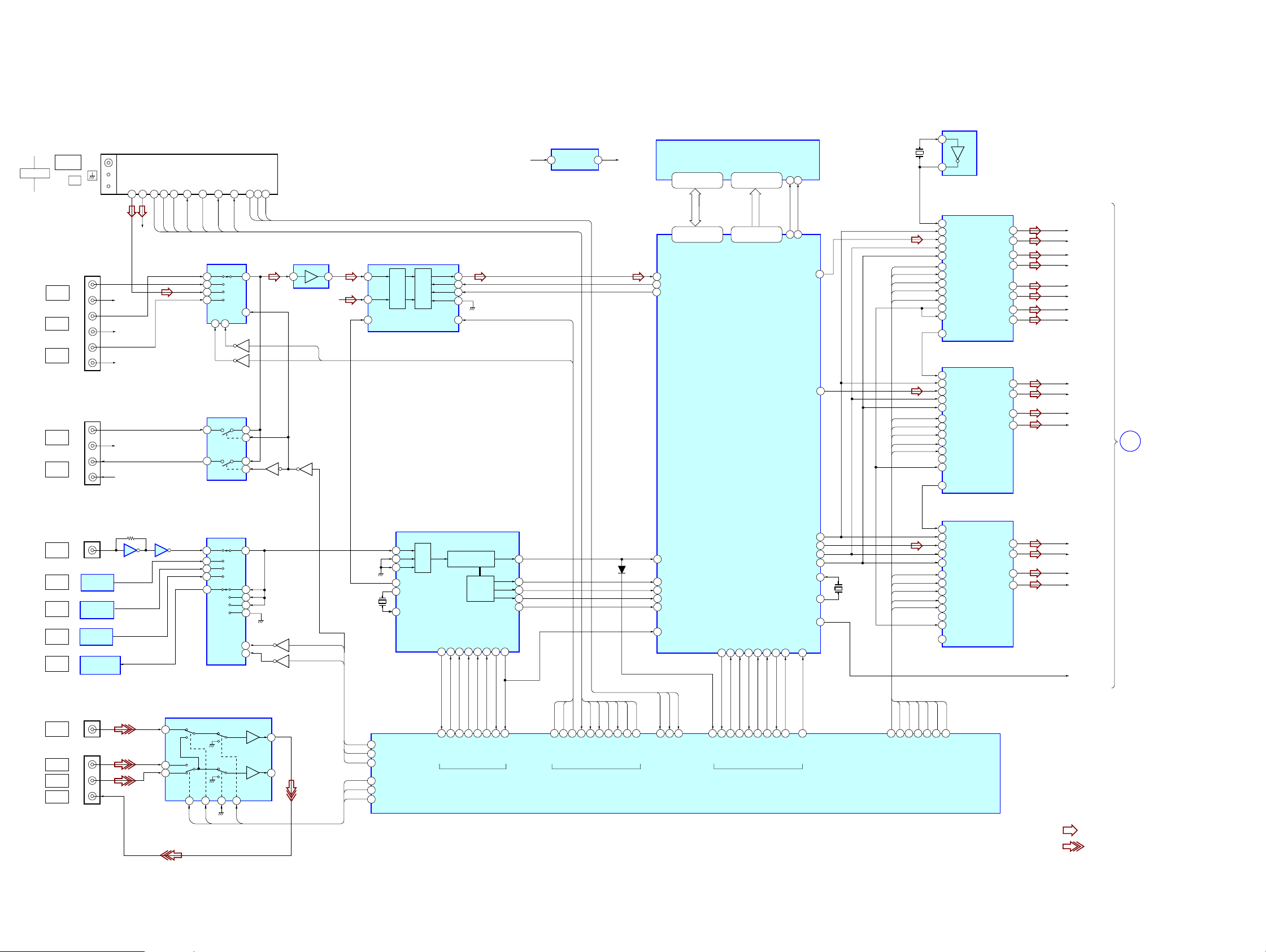
4-2. BLOCK DIAGRAM – TUNER/DSP SECTION –
ANNTENA
COAXIAL
FM 75Ω
TV/SAT
IN
DVD
IN
VIDEO
IN
HDD/MD
IN
HDD/MD
OUT
SDRAM
IC116
IC114
+2.6V
1 3
TUNER UNIT
AM
MUTE
STEREO
LCH
RCH
MUTE
TUNEDCECE
STEREO
TUNED
DI
810117 6 1514134321
ST-DI/
MC-DO
ST-DO/
DO
MC-DI
SCLK
CLK
RDS-DATA
R-DATA
RDS-INT
FSO
R-INT
TU901
FM SIG OUT
REG.
R-CH
INPUT SELECT
IC108
J102
L
R
R-CH
L
R
R-CH
L
R
R-CH
X0 X
12
X1
14
X2
15
X3
11
AB
10 9
INH
13
6
Q105
BUFFER
A/D CONVERTOR
IC112
3 11
A/D
RIN
R-CH
52B
52A
5
16 6
SYSCLK
IC113
DOUTLIN
BCK
LRCK
FSYNC
INTERFACE
SERIAL DATA
RSTB
15
14
13
12
PD
Q106
INPUT/OUTPUT SELECT
2
8
IC106
1
13
9
6
Q104 Q103
J103
L
R
R-CH
L
R
R-CH
+2.6V+5V
18
17
15
D0 - 15
7 - 10,13 - 16,29 - 32,
35 - 38
108,107,105 - 102,
99,98,80 - 77,75 - 72
D0 - 7
D8/GP0 - D15/GP7
SDI1
BCK1
LRCK1
A0 - 15
5 - 1,44 - 42,27,26,
31,32,21 - 18
112,110,109,97 - 92,
85 - 82,66 - 64
A0 - 15
17 6
45 44
WE
WE0
CS
CS0
SDO1
23
AUDIO DSP
IC115
SD03
25
X401
49.152MHz
INIT
NSMUTE
LAT1
SHIFT
SCDT
INIT
NSMUTE
LAT2
SHIFT
SCDT
CLOCK OSC
IC403
2
4
PCM/PWM CONVERTOR
XFSOIN
36
FS-IN
21
DATA
18
BCK
17
LRCK
16
15
INIT
NSPMUT
14
SCLATC
13
SCSHIF
12
SCDT
11
FSCKO
22
FSOI
23
FSOUT
6
PCM/PWM CONVERTOR
36 XFSOIN
FS-IN
21
DATA
18
BCK
17
LRCK
16
15
INIT
NSPMUT
14
SCLATC
13
SCSHIF
12
SCDT
11
FSCKO
22
NC
FSOI
23
FSOUT
6
IC405
IC408
HPOUTL1
HPOUTL2
HPOUTR1
HPOUTR2
OUTL1
OUTL2
OUTR1
OUTR2
OUTL1
OUTL2
OUTR1
OUTR2
33
31
29
27
2
4
41
39
2
4
41
39
HP - L (+)
HP - L (–)
HP - R (+)
HP - R (–)
FL (+)
FL (–)
FR (+)
FR (–)
C (+)
C (–)
WO (+)
WO (–)
DISPLAY/POWER
A
SECTION
(Page 14)
DVD
COAX IN
DVD
OPT IN
TV/SAT
OPT IN
HDD/MD
OPT IN
HDD/MD
OPT OUT
VIDEO
IN
DVD
IN
TV/SAT
IN
MONITOR
OUT
J101
IC101
OPTICAL
RECEIVER
IC102
OPTICAL
RECEIVER
IC103
OPTICAL
RECEIVER
IC104
OPTICAL
TRANSMITTER
J701
J702
WAVE SHAPER
IC107
3
56 2
12
1
3
A
VIDEO
SELECT
IC105
1C0 1Y
6
1C1
5
1C2
4
1C3
3
2Y
9
VIDEO SELECT
IC701
4132
B
7 3
2C0
10
2C1
2C2
2C3
11
12
13
Q102
A
14
2
B
4066
153A
153B
X101
12.288MHz
Q101
10
4066
153A
153B
5
NC
A
B
11
C
C
NJU4066
70
TC74153H-A
69
TC74153H-B
68
22
VIDEO-SW-A
26
VIDEO-SW-B
VIDEO-SW-C
24
NC
NC
LAT2
LAT3
LAT2(C/SW)
LAT3(SL/SR)
16 XFSOIN
21
18
17
16
15
14
13
12
11
22
23
SHIFT
SHIFT
PCM/PWM CONVERTOR
IC411
FS-IN
DATA
BCK
LRCK
INIT
NSPMUT
SCLATC
SCSHIF
SCDT
FSCKO
FSOI
FSOUT
6
SCDT
SCDT
OUTL1
OUTL2
OUTR1
OUTR2
2
4
41
39
SL (+)
SL (–)
SR (+)
SR (–)
EN
DIGITAL AUDIO
I/F RECEIVER
IC111
SCKOUT
14
SDO2
24
BCKO
4
INPUT
XMCK
XOUT
XIN
CIRCIT
5
20
21
22
DATA
DEMODULATOR
TIMING
XSTATE
XMODE
CKSEL1
CLKCEDIDOERROR
47 3817 48 37 36 35 34
94 95
100
93 96 97 98 99 72 759 71 74 73 78 14 53 5276 15
CE
CLK
XMODE
XSTATE
CKSEL1
DIR TUNER DSP
DI
BCK
LRCK
CKOUT
AUDIO
DO
16
14
15
13
24
ERROR
PD
52B
PD
52A
MUTE
TC4052B
TC4052A
STEREO
TUNEDCEDIDOCLK
MUTE
TUNED
STEREO
DATA
SLATCH
D102
DO
CLK
30
SDI-2
BCK-2
29
28
LRCK-2
22
KFSIO
69
GP8
59
EXLOCK
R-DATA
R-INT
FSO
40
RDS-INT
RDS-DATA
FM SIG OUT
SYSTEM CONTROL
HDOUT
HCLK
HDIN
HACN
HCS
HDIN
HACN
HCS
BST
BST
34 3335 32 36 56 68
20 19
1 18 5 4 3 2 7
HCLK
DATAO
HDOUT
GP9PMXRST
113
GP9
20
LRCKO
19
MCLK1
9
X102
13.5MHz
12
MCLK2
EN
92
2
PM
XRST
INIT
NSMUTE
LAT3
SHIFT
SCDT
INIT
85 86 89 60 596
RST(INIT)
MSMUTE
LAT1
91 90
MSMUTE
LAT1(L/R)
IC118 (1/2)
•Signal Path
: FM
: VIDEO
1414
 Loading...