

Page 1
STR-KSL600
SERVICE MANUAL
Ver 1.0 2004.08
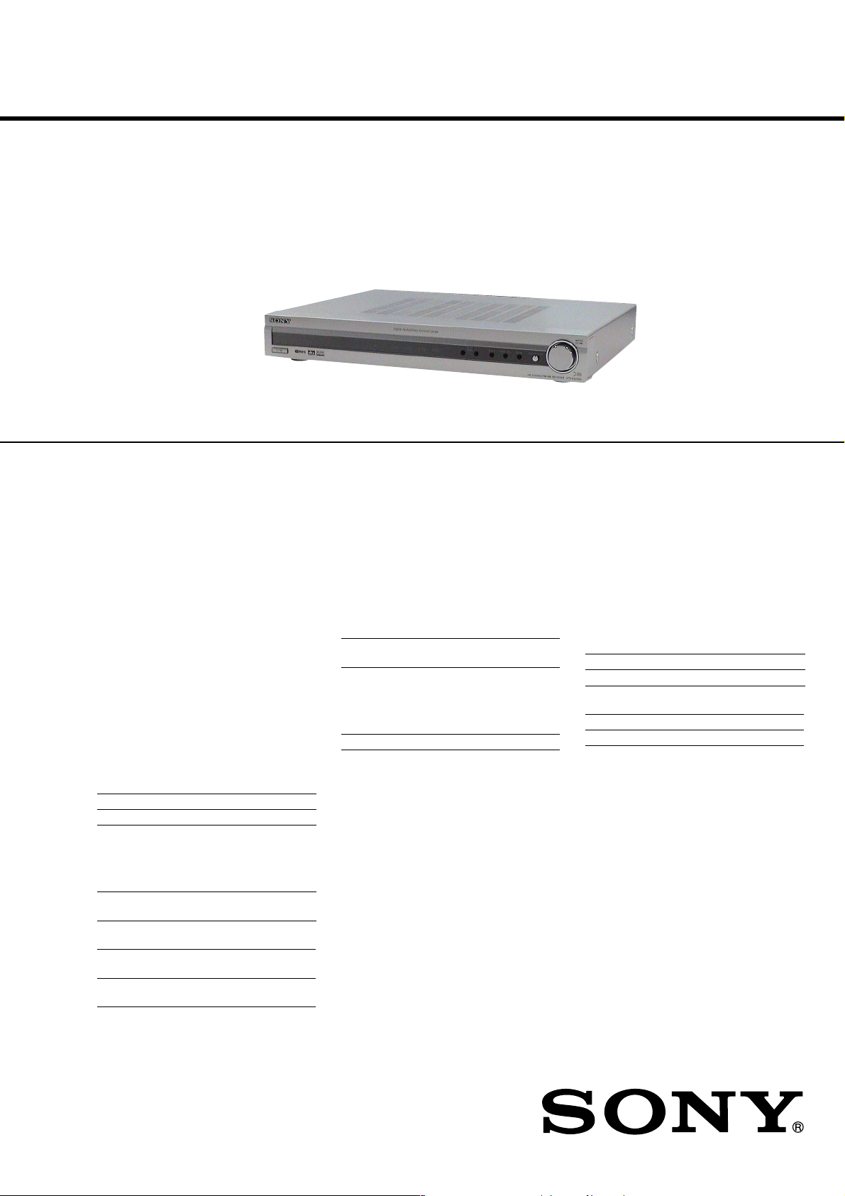
STR-KSL600 is the receiver section in HT-SL600/SL800.
This receiver incorporates Dolby* Digital and Pro
Logic Surround and the DTS** Digital Surround
System.
* Manufactured under license from Dolby
Laboratories.
“Dolby”, “Pro Logic” and the double-D symbol are
trademarks of Dolby Laboratories.
**“DTS” and “DTS Digital Surround” are registered
trademarks of Digital Theater Systems, Inc.
AEP Model
UK Model
Amplifier section
Power Output
Models of area code CEL, CEK
(6 ohms 1 kHz, THD 0.7%)
(6 ohms 1 kHz, THD 10%)
1) Measured under the following conditions:
Area code Power requirements
CEL, CEK 230 V AC, 50 Hz
2) Depending on the sound field settings and the
source, there may be no sound output.
Inputs (Analog)
TV/SAT, DVD, VIDEO Sensitivity: 500 mV
Inputs (Digital)
DVD (Coaxial) Sensitivity: −
DVD, TV/SAT (Optical) Sensitivity: −
1)
FRONT2): 40 W/ch
2)
CENTER
SURR
1)
FRONT2): 60 W/ch
CENTER
SURR
Impedance: 50 kiloohms
Impedance: 75 ohms
Impedance: −
: 40 W
2)
: 40 W/ch
2)
: 60 W
2)
: 60 W/ch
SPECIFICATIONS
Outputs (Analog)
SUB WOOFER Voltage: 2 V
Impedance: 1 kiloohm s
Reproduction frequency range:
28 − 20,000 Hz
Tone
Gain levels ±6 dB, 1 dB step
FM tuner section
Tuning range 87.5 − 108.0 MHz
Antenna FM wire antenna
Antenna terminals 75 ohms, unbalanced
Intermediate Frequency 10.7 MHz
AM tuner section
Tuning range
Models of area code CEL, CEK
With 9-kHz tuning scale: 531 − 1,602 kHz
Antenna Loop antenna
Intermediate Frequency 450 kHz
Video section
Inputs/Outputs
Video: 1 Vp-p, 75 ohms
General
Power requirements
Area code Power requirements
CEL, CEK 230 V AC, 50/60 Hz
Power consumption
Area code Power consumption
CEL, CEK 170 W
Power consumption (during st an dby mode)
0.3 W
Dimensions (w/h/d) (Approx.)
430 × 352 × 66 mm
including projecting parts
and controls
Mass (Approx.) 5.5 kg
Design and specifications are subject to change
without notice.
9-879-050-01
2004H05-1
© 2004.08
FM STEREO/FM-AM RECEIVER
Sony Corporation
Audio Group
Published by Sony Engineering Corporation
Page 2

STR-KSL600
Notes on chip component replacement
• Never reuse a disconnected chip component.
• Notice that the minus side of a tantalum capacitor may be
damaged by heat.
TABLE OF CONTENTS
1. SERVICING NOTES ............................................... 3
2. GENERAL ................................................................... 4
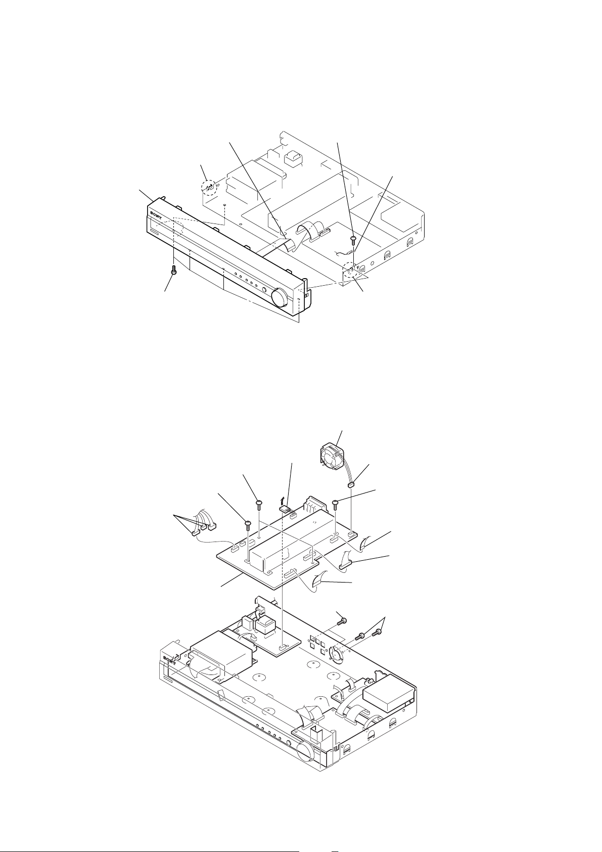
3. DISASSEMBLY
3-1. Disassembly Flow ........................................................... 5
3-2. Case (SL500)................................................................... 5
3-3. Front Panel Section ......................................................... 6
3-4. MAIN Board.................................................................... 6
4. TEST MODE.............................................................. 7
5. DIAGRAMS
5-1. Block Diagram − AUDIO DSP/VIDEO Section − ......... 8
5-2. Block Diagram − TUNER/AUDIO AMP Section −....... 9
5-3. Block Diagram
− DISPLAY/POWER SUPPLY Section −....................... 10
5-4. Printed Wiring Board
− DIGITAL Board (Component Side) − ......................... 12
5-5. Printed Wiring Board
− DIGITAL Board (Conductor Side) − ........................... 13
5-6. Schematic Diagram − DIGITAL Board (1/4) −.............. 14
5-7. Schematic Diagram − DIGITAL Board (2/4) −.............. 15
5-8. Schematic Diagram − DIGITAL Board (3/4) −.............. 16
5-9. Schematic Diagram − DIGITAL Board (4/4) −.............. 17
5-10. Printed Wiring Board − I/O Board − .............................. 18
5-11. Schematic Diagram − I/O Board − ................................. 19
5-12. Printed Wiring Board − MAIN Board − ......................... 20
5-13. Printed Wiring Board − STBY Board − ......................... 21
5-14. Schematic Diagram − MAIN Section (1/2) − ................ 22
5-15. Schematic Diagram − MAIN Section (2/2) − ................ 23
5-16. Printed Wiring Boards − PANEL Section − ................... 24
5-17. Schematic Diagram − PANEL Section − ....................... 25
SAFETY-RELATED COMPONENT WARNING!!
COMPONENTS IDENTIFIED BY MARK 0 OR DOTTED LINE
WITH MARK 0 ON THE SCHEMATIC DIAGRAMS AND IN
THE PARTS LIST ARE CRITICAL TO SAFE OPERATION.
REPLACE THESE COMPONENTS WITH SONY PAR TS WHOSE
PART NUMBERS APPEAR AS SHO WN IN THIS MANU AL OR
IN SUPPLEMENTS PUBLISHED BY SONY.
6. EXPLODED VIEWS
6-1. Front Panel Section ......................................................... 35
6-2. Chassis Section ................................................................ 36
7. ELECTRICAL PARTS LIST................................ 37
2
Page 3
SECTION 1
SERVICING NOTES
STR-KSL600
UNLEADED SOLDER
Boards requiring use of unleaded solder are printed with the leadfree mark (LF) indicating the solder contains no lead.
(Caution: Some printed circuit boards may not come printed with
the lead free mark due to their particular size)
: LEAD FREE MARK
Unleaded solder has the following characteristics.
• Unleaded solder melts at a temperature about 40 °C higher
than ordinary solder.
Ordinary soldering irons can be used but the iron tip has to be
applied to the solder joint for a slightly longer time.
Soldering irons using a temperature regulator should be set to
about 350 °C.
Caution: The printed pattern (copper foil) may peel away if
the heated tip is applied for too long, so be careful!
• Strong viscosity
Unleaded solder is more viscou-s (sticky, less prone to flow)
than ordinary solder so use caution not to let solder bridges
occur such as on IC pins, etc.
• Usable with ordinary solder
It is best to use only unleaded solder but unleaded solder may
also be added to ordinary solder.
• MODEL IDENTIFICATION
– Back Panel –
PART No.
MODEL PART No.
AEP model 4-254-456-2[]
UK model 4-254-456-3[]
3
Page 4
STR-KSL600
2 3 4 5 6 8 9 q;qaqsq
q
7
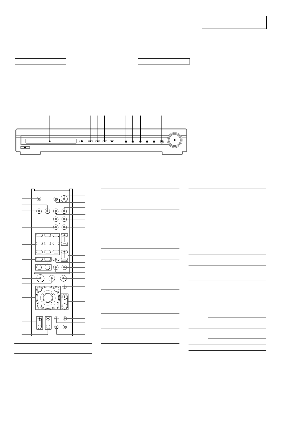
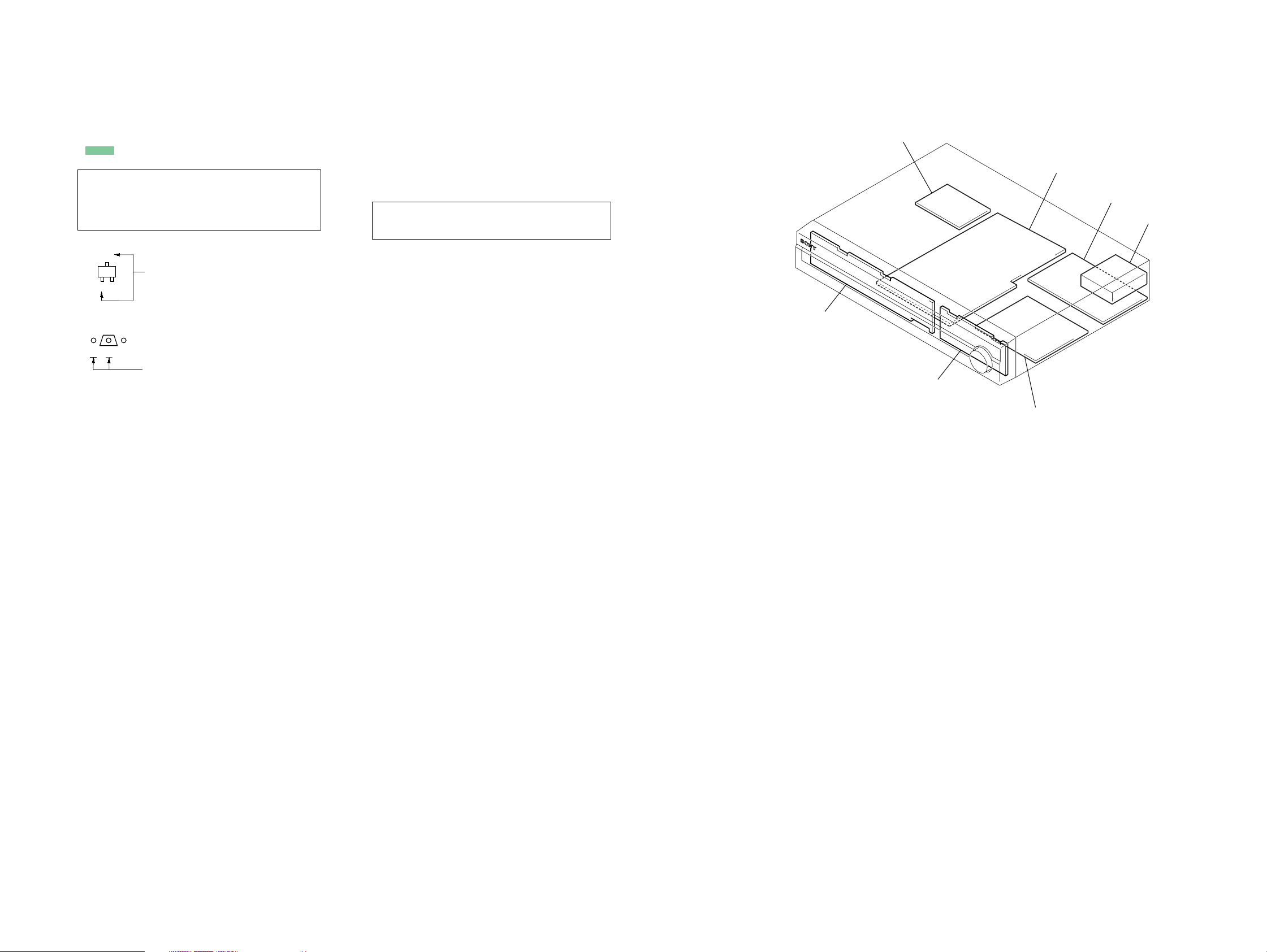
LOCATION OF CONTROLS
– Front Panel –
SECTION 2
GENERAL
This section is extracted from
instruction manual.
ALPHABETICAL ORDER NUMBERS AND SYMBOLS
Display 2
DVD (indicator) 5
INPUT SELECTOR
qd
IR (receptor) 3
MASTER VOLUME qf
1
MUTING qs
PRESET TUNING + 9
PRESET TUNING − 8
SOUND FIELD qa
TUNER (indicator) 7
TV/SAT (indicator) 6
VIDEO (indicator) 4
?/1 (power) 1
; PLII q;
d
f
– Remote Commander –
SEARCH MODE
X
F
f
RETURN/EXIT
SAT TV
AUX
;
PL/PL A.F.D.
D.TUNING
SUBTITLE
-
AV MENU
g
O
TV/
VIDEO
WIDE
?/1
SLEEP
TUNER
SOUND
FIELD
PRESET/
CH/D.SKIP
x
MUTING
MASTER
VOL
MAIN
MENU
TEST
TONE
ea
e;
wl
wk
wj
wh
wg
wf
wd
ws
wa
w;
ql
qk
qj
qh
1
2
3
4
5
6
7
8
9
q;
qa
qs
TV ?/1 AV ?/1
SYSTEM STANDBY
VIDEO DVD
DUAL
MONO
FM MODE
123
ANGLE
AUDIO
456
SWAP JUMP
TIME
789
MEMORY SHIFT
>
.
0/10 >10/11 ENTER/12
TUNING DISC ALT
M
m
ANT
CLEAR
H
TOP MENU/
GUIDE
G
ENTER
DISPLAY
TV VOL TV CH
qg
qd
Remote
Button
A.F.D. wh Receiver Selects A.F.D. AUTO.
ALT ws Remote When ALT button lights
Operations Function
up, it changes the remote
key function to activate
those buttons with orange
printing.
qf
Remote
Button
ANGLE 6 DVD player Selects viewing angle or
ANT 8 VCR Selects output signal
AUDIO 6 TV/VCR/
AUX 4 Receiver To listen to an audio
AV MENU qaVCR/
AV ?/1 e;TV/VCR/
CLEAR 8 DVD player Press if you make a
DISC wa CD player Selects a disc directly
DISPLAY qaTV/VCR/
D.TUNING 6Receiver Enters direct tuning
DUAL
MONO 6
DVD 2 Receiver To watch DVD.
Operations Function
changes the angles.
from the antenna
terminal: TV signal or
VCR program.
Changes the sound to
DVD player
Multiplex or Bilingual
or Multi Channel TV
Sound.
equipment.
Displays menu.
satellite tuner/
DVD player
Turns the audio and
CD player/
DVD player
video components on or
off.
mistake when you press
the numeric button or
press to return to
continuous play etc.
(multi-disc changer
only).
Selects information
DVD player
displayed on the TV
screen.
mode.
Receiver Selects the la ng uage
you want during digital
broadcast.
Remote
Button
ENTER qa Receiver/
Operations Function
Enters the selection.
VCR/
satellite tuner/
DVD player
ENTER/12 wdTV/VCR/
Enters the selection.
satellite tuner
FM MODE 6Receiver Selects FM monaural o r
stereo reception.
JUMP 6 TV Toggles between the
previous and the current
channels.
MAIN
MENU qj
MASTER
VOL +/–
Receiver Selects the menu of the
receiver.
Receiver Adjusts the master
volume of the receiver.
qk
MEMORY 7Receiver Stores the radio stations.
MUTING qlReceiver Mutes the sound from
the receiver.
PRESET/ Receiver Selects preset stations.
CH/D.SKIP
+/– wf
RETURN/
EXIT/O
TV/VCR/
Selects preset channel.
satellite tuner
CD player/
DVD player
Skips discs (multi-disc
changer only).
DVD player Returns to the previous
menu or exits the menu.
qa Satellite tuner Exits the menu.
SAT wk Receiver To watch satellite tuner.
SEARCH
MODE wa
DVD player Selects searching mode.
Press to select the unit
for search (track, in dex,
etc.)
4
Page 5
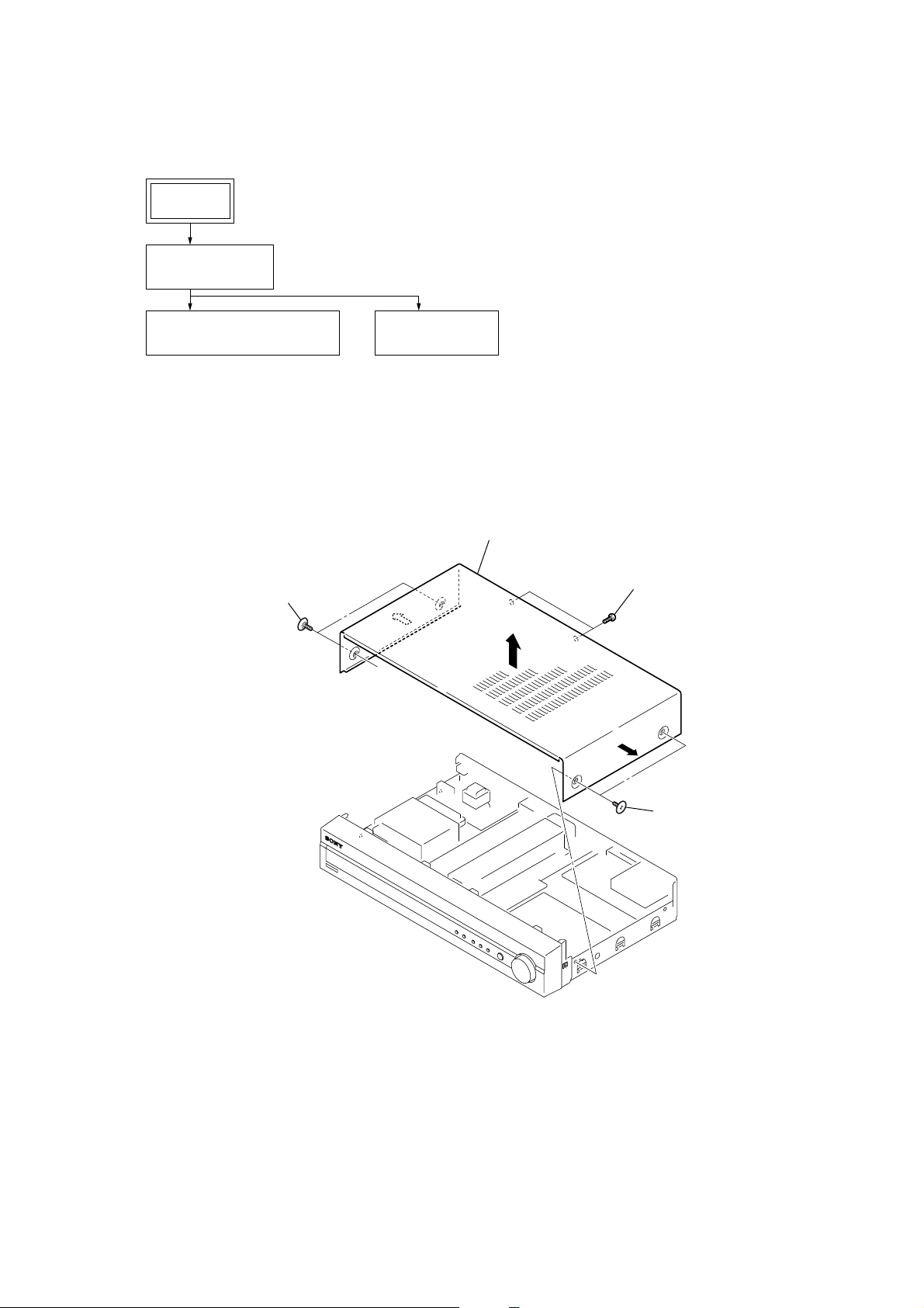
• This set can be disassembled in the order shown below.
3-1. DISASSEMBLY FLOW
SET
3-2. CASE (SL500)
(Page 5)
STR-KSL600
SECTION 3
DISASSEMBLY
3-3. FRONT PANEL SECTION
(Page 6)
Note: Follow the disassembly procedure in the numerical order given.
3-4. MAIN BOARD
(Page 6)
3-2. CASE (SL500)
5
2
two tapping screws
3
case (SL500)
4
1
two screws
(BV/ring)
3
2
two tapping screws
5
Page 6
STR-KSL600
3-3. FRONT PANEL SECTION
6
front panel section
4
four screws
(BVTP3 × 8)
1
wire (flat type) (17 core)
(CNS193)
5
claw
2
screw
(BVTP3
5
×
6)
3
lead (with connector)
claw
3-4. MAIN BOARD
6
three connectors
(CNP801, CNP802, CNP804)
8
screw
(BVTP3 × 10)
0
MAIN board
9
two screws
(BVTP3 × 6)
6
connector
(CNP903)
7
two screws
(BV/ring)
3
D.C. fan
(M1)
2
connector
(CNP861)
8
screw
(BVTP3 × 10)
4
6
5
wire (flat type) (19 core)
(CNS822)
1
wire (flat type) (11 core)
(CNS402)
connector
(CNP821)
two screws
(BV/ring)
6
Page 7

SECTION 4
TEST MODE
STR-KSL600
FACTORY PRESET MODE
All preset contents are reset to the default setting.
Procedure:
1. While pressing the PLII and [PRESET TUNING +] buttons,
press the I/1 button to turn on the main power.
2. The message “FACTORY” appears and the present contents
are reset to the default values.
ALL CLEAR MODE
All preset contents are cleared when this mode is activated. Use
this mode before returning the product to clients upon completion
of repair.
Procedure:
1. While pressing the PLII and [PRESET TUNING --] buttons,
press the I/1 button to turn on the main power.
2. The message “CLEARING !” appears and the memories are
reset to the default values.
3. When done, the message “CLEARED” appears.
FL CHECK MODE
All fluorescent segments are tested. When this test is activated, all
segments turn on at the same time, then each segment turns on one
after another.
Procedure:
1. While pressing the [MUTING] and [PRESET TUNING --] buttons,
press the I/1 button to turn on the main power.
2. All segments and all LEDs turn on.
3. Press the [INPUT SELECTOR] button.
4. Half of segments and [VIDEO], [TUNER] LEDs turn on.
5. Press the [INPUT SELECTOR] button once again.
6. Others half of segments and [DVD], [TV/SAT] LEDs turn on.
7. Press the [INPUT SELECTOR] button once again.
8. All segments and all LEDs turn off.
SOUND FIELD CLEAR MODE
The preset sound field is cleared when this mode is activated. Use
this mode before returning the product to clients upon completion
of repair.
Procedure:
1. While pressing the [SOUND FIELD] button, press the I/1
button to turn on the main power.
2. The message “SF. CLR.” appears and initialization is
performed.
RDS AUTOBETICAL MODE
Procedure:
1. While pressing the [INPUT SELECTOR] button, press the I/1
button to turn on the main power.
2. The message “AUTO-BET” appears and scans and stores all
the FM and FM RDS stations in the broadcast area.
3. When done, the message “FINISH” appears.
VERSION MODE
When this mode is used, the model, the destination and the software
version number are displayed.
Procedure:
1. While pressing the [SOUND FIELD] and [PRESET TUNING --]
buttons, press the I/1 button to turn on the main power.
2. The model, the destination and the software version number
appear.
KEY CHECK MODE
This mode is used to check the key.
Procedure:
1. While pressing the [MUTING] and [INPUT SELECTOR] buttons,
press the I/1 button to turn on the main power.
2. The message “REST 06” appears.
3. Every pressing of any button other than the I/1 button counts
down the buttons. The b uttons which are already counted once
are not counted again.
4. When all buttons are pressed, the message “REST 00” appears.
PROTECTOR AUTO OFF MODE
When this mode is used, a protector on state is maintainable.
Procedure:
1. While pressing the [MUTING] and PLII buttons, press the I/1
button to turn on the main power.
2. The message “PROT EVER” appears.
STR-KSL600
77
Page 8
STR-KSL600
SECTION 5
DIAGRAMS
5-1. BLOCK DIAGRAM – AUDIO DSP/VIDEO Section –
(Page 9)
A
DIGITAL
L-CH
TV/SAT
OPT IN
DVD
OPT IN
DVD
COAX IN
DIGITAL OPTICAL
RECEIVER
IC301
DIGITAL OPTICAL
RECEIVER
IC302
J301
IC303
R-CH
A/D CONVERTER
IC1401
2 9AINL SDTO
1AINR
MCLK
13
11
X1301
12.288MHz
20
22
21
XIN
XOUT
XMCK
4DIN1
3DIN0
5DIN2
PDN
S-RAM
IC1502
D0 – D15 A0 – A15
7 – 10, 13 – 16,
29 – 32, 35 – 38
5 – 1, 44 – 42,
27 – 24, 21 – 18
WEWE0
CSCE0
17
6
R-ch is omitted due to same as L-ch.
SIGNAL PATH
: AUDIO (ANALOG)
: AUDIO (DIGITAL)
: VIDEO
108, 107, 105 – 102,
99, 98, 80 – 77, 75 – 72
18 SDI1
30 SDI2
12SCLK
10LRCK
16DATA0
14BCK
15LRCK
13CKOUT
24AUDIO
35DO
36DI
38CLK
37CE
48XMODE
17 BCKI1
29 BCKI2
15 LRCKI1
28 LRCKI2
22 KFSIO
69 GP8
59 EXLOCK
12 AD5380_PDN
D1301
1 DATAO
98 DO
97 DI
95 CLK
96 CE
93 XMODE
D0 – D15
HDINHDIN
33
19
ANA/DIG
24
D1103
HCLKHCLK
34
20
SYSTEM CONTROLLER
ERROR
99
112, 110, 109, 97 – 92,
AUDIO DIGITAL
SIGNAL PROCESSOR
IC1501
HCSHCS
HDOUTHDOUT
HACNHACN
GP9GP9
36
35
32
68
4
18
5
2
IC1601 (1/3)
XSTATE
100
82 – 85, 66 – 64
A0 – A15
BSTBST
GP12GP12
PMPM
56
37
113
3
8
7
2
6
XRSTXRST
X1101
16.5MHz
83
X1
F.MUTE
21
D1106
45
44
23SDO1
24SDO2
25SDO3
20BCKO
19LRCKO
14SCKOUT
MCLK2
MCLK1
12
9
X1502
13.9MHz
82
X0
25VIDEO-SW1
26VIDEO-SW2
32VIDEO-MUTE
34SDA
33SCL
5 SDA
6 SCL
EEPROM
IC1131
SDO1 SDO1, SDO2, SDO3
SDO2
SDO3
BCKO
LRCKO
SCKO
VIDEO AMP & SWITCH
IC201
3V2
12 V1
SW12SW213M24M1
10MON
11
BCKO, LRCKO, SCKO
J501 (1/2)
VIDEO
DVD
MONITOR
OUT
VIDEO IN
B
C
(Page 9)
(Page 9)
STR-KSL600
17XSTATE
34ERROR
DIGITAL AUDIO INTERFACE RECEIVER
IC1301
MUTING SWITCH
Q1105
D1105
MUTING SWITCH
Q1103
MUTING SWITCH
Q1104
SMUTE
D
(Page 9)
88
Page 9
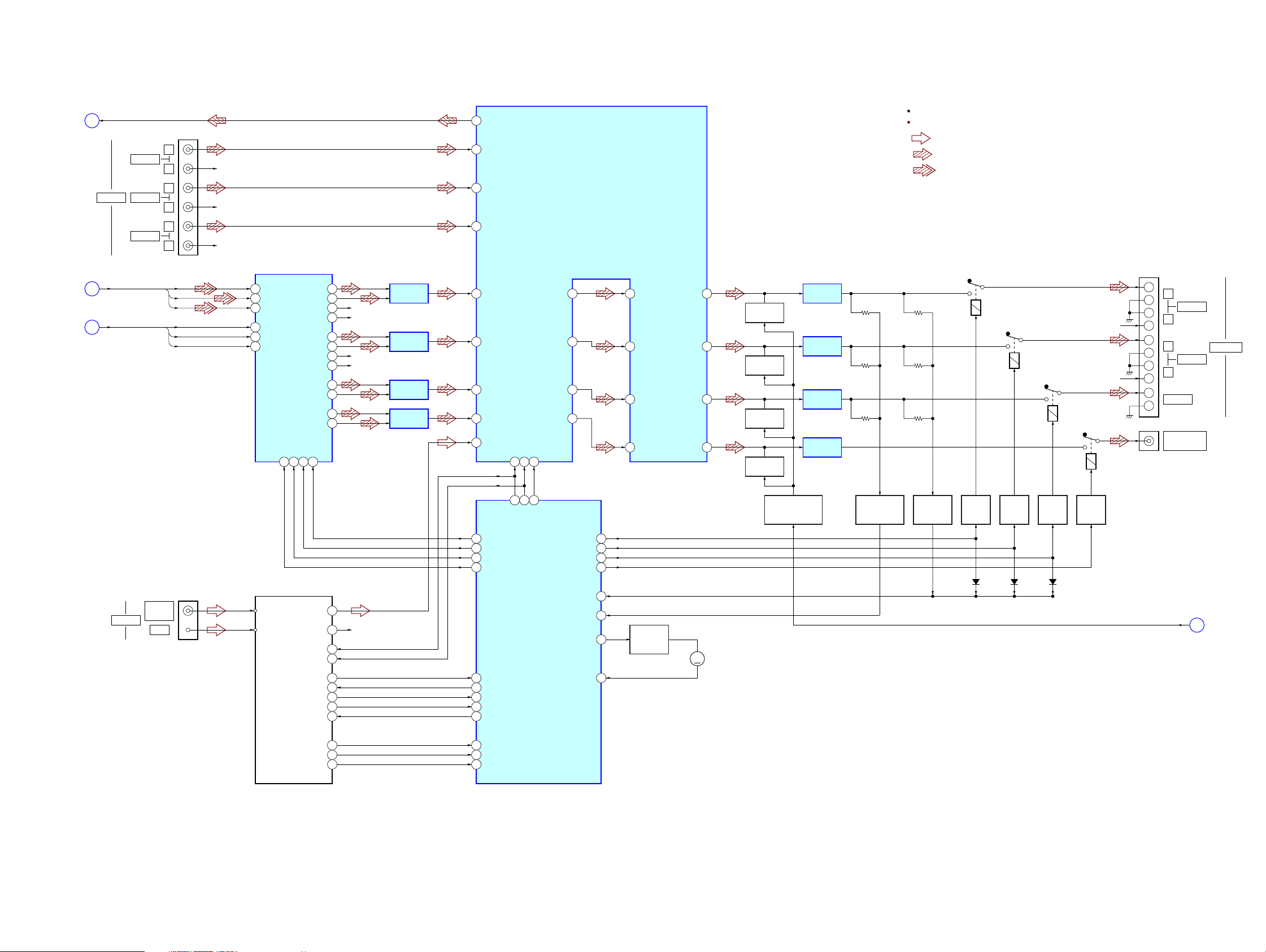
5-2. BLOCK DIAGRAM – TUNER/AUDIO AMP Section –
STR-KSL600
A
(Page 8)
AUDIO IN
B
(Page 8)
C
(Page 8)
L-CH
VIDEO
DVD
TV/SAT
J501 (2/2)
L
R
L
R
L
R
SDO1SDO1, SDO2, SDO3
SDO2
SDO3
BCKOBCKO, LRCKO, SCKO
LRCKO
SCKO
R-CH
R-CH
R-CH
D/A CONVERTER
8 SDTI3
6 SDTI1
7 SDTI2
5 BICK
9 LRCK
4 MCLK
IC1452
CDTI12CCLK11CSN10PDN
3
14 BAL L+
R-ch is omitted due to same as L-ch.
SIGNAL PATH
: TUNER
70 INL8
AUDIO SELECTOR, ELECTRICAL VOLUME
74 INL6
78 INL4
18LOUT3+
17LOUT3–
16ROUT3+
R-CH
15ROUT3–
R-CH
26LOUT1+
25LOUT1–
24ROUT1+
R-CH
23ROUT1–
R-CH
22LOUT2+
21LOUT2–
20ROUT2+
19ROUT2–
MIX AMP
IC1403
MIX AMP
IC1405
MIX AMP
IC1404 (1/2)
MIX AMP
IC1404 (2/2)
20 LINL2 55 LVIN
23 SLINL2
24 CIN2
25 SWIN2
2 INL2
28
DATA
CLK27LATCH
29
IC401
56LSELOUT
39SLSELOUT
38CSELOUT
33SWSELOUT
40 SLVIN
37 CVIN
34 SWVIN
54LOUT
MUTING
Q361
41SLOUT
MUTING
Q365
36COUT
MUTING
Q363
37SWOUT
MUTING
Q364
POWER AMP
IC701
POWER AMP
IC601
POWER AMP
IC501
LINE AMP
IC402
: AUDIO (ANALOG)
: AUDIO (DIGITAL)
RY701
RY601
RY501
RY401
R-CH
R-CH
TM601
+
+
+
+
+
J403
L
–
–
R
L
–
–
R
CENTER
–
SUB WOOFER
FRONT
SPEAKERS
SURR
OUT
ANTENNA
FM 75Ω
COAXIAL
AM
FM
AM
TN1
TUNER UNIT
RDS DATA
RDS INT
FM SIG OUT
16
15
22
CLK
DATA
LATCH
9 AK4355_PDN
12 AK4355_CSN
14 AK4355_CLK
13 AK4355_CDT
8L CH
10R CH
R-CH
3DATA
1CLOCK
2
DO
69 DO
68 SLATCH4CE
66 TUNED6TUNED
65 STEREO7STEREO
64 MUTE11MUTING
5315
5214
4313
SYSTEM CONTROLLER
RDA DATA
RDS CLK
RDS SIGNAL
IC1601 (2/3)
70PREOUT/FRONT RELAY
72RAR RELAY
71CENTER RELAY
17WOOFER RELAY
67PROTECTOR
76FAN_ON
74F_CTRL2
75FAN_CLK
FAN MOTOR
DRIVE
Q861 – 863
M1
M
(FAN)
MUTING
CONTROL SWTICH
Q379
FAN MOTOR
LEVEL DETECT
Q550, 551
AC POWER
PROTECTOR
Q730 – 732
RELAY
DRIVE
Q720
D721,
D1110
RELAY
DRIVE
Q620
D621,
D1108
RELAY
DRIVE
Q520
D521,
D1107
RELAY
DRIVE
Q402
SMUTE
D
(Page 8)
STR-KSL600
99
Page 10
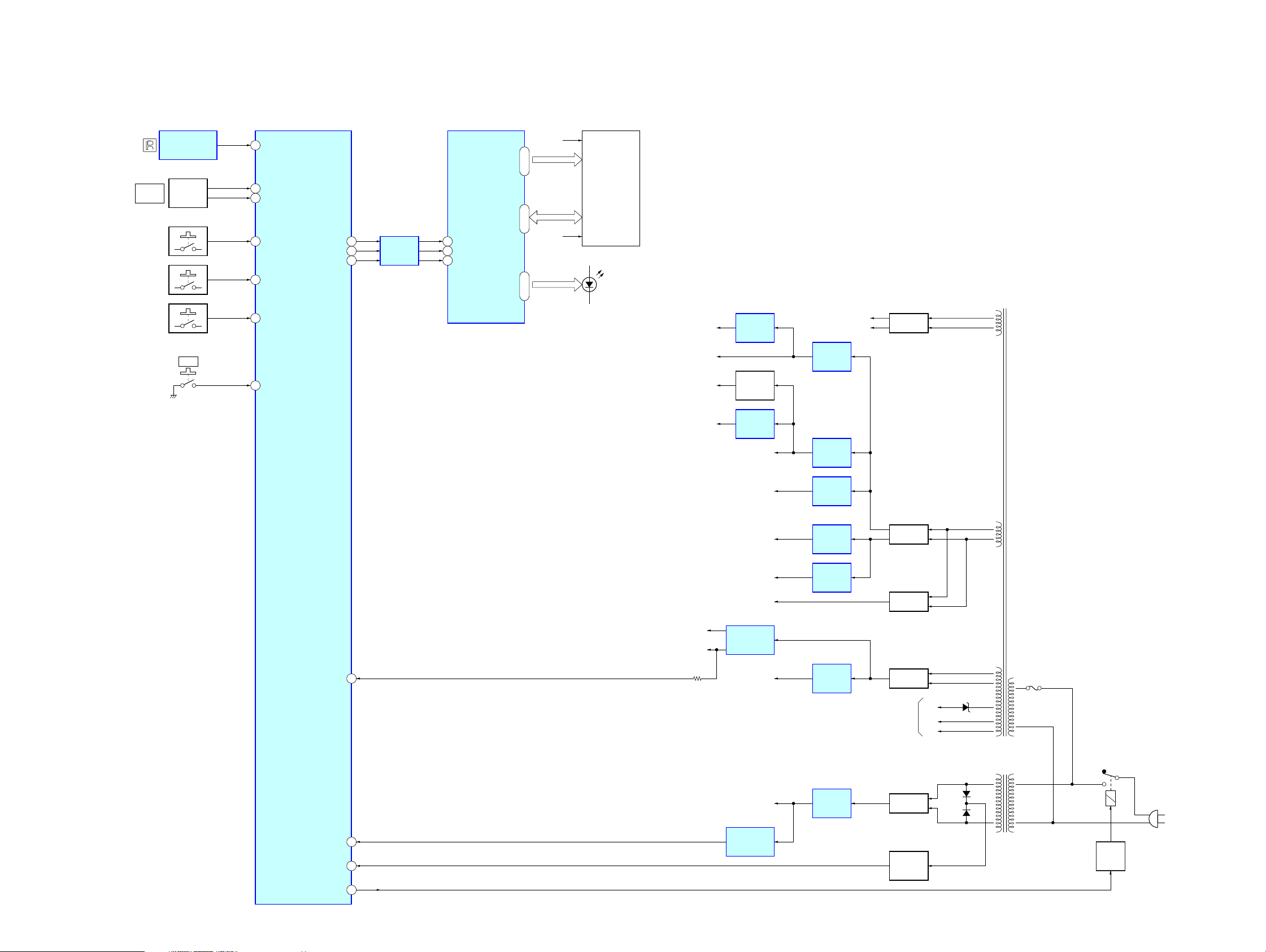
STR-KSL600
FL1001
FLUORESCENT
INDICATOR
TUBE
F1
F2
GRID1 – GRID12
54 SIRCS
60 VOL (A)
59 VOL (B)
38 A/D0 7 DIN
FLUORESCENT INDICATOR TUBE DRIVER,
LED DRIVER
IC152
REMOTE CONTROL
RECEIVER
IC102
MASTER
VOLUME
ROTARY
ENCODER
RV101
S120, 121
39 A/D1S117, 118
40 A/D2
56 POWER KEY
S119, 122
S123
I
/ 1
42 – 31
SEG1 – SEG16
14 – 291 – 4
D151 – 154
TUNER LED,
TV/SAT LED,
DVD LED,
VIDEO LED
61DIN
8 CLK
62CLK
9 STB
63FL_STB
78POWER RELAY
48STOP
77RSTX
55FUSE DETECT
LEVEL SHIFT
IC1651
(AC IN)
RY901
RELAY
DRIVE
Q951
T902
SUB POWER
TRANSFORMER
T901
MAIN POWER
TRANSFORMER
D957
D956
AC POWER
DETECT
Q901
RECT
D952 – 955
RECT
D805 – 808
+3.3V
REGULATOR
IC1904
RECT
D814 – 817
RECT
D801 – 804
+5V
REGULATOR
IC1031
–7V
REGULATOR
IC404
–5V
REGULATOR
IC406
RESET SIGNAL
GENERATOR
IC1111
STBY +3.3V
+3.3V/+2.6V
REGULATOR
IC1901
+5V
REGULATOR
IC1001
+5V
RELAY B+
–7V
V–5V
+5V
REGULATOR
IC405
V+5V
+7V
REGULATOR
IC403
+10V
REGULATOR
IC1902
+7V
F901
F1
–27V
F2
FLUORESCENT INDICATOR TUBE
(FL101)
D813
RECT
D809
D+3.3V
D+2.6V
A+5V, D+5V
+3.3V
REGULATOR
Q401
+3.3V
+3.3V
REGULATOR
IC1071
TUNER+3.3V
TUNER+10V
B+
B–
SYSTEM CONTROLLER
IC1601 (3/3)
5-3. BLOCK DIAGRAM – DISPLAY/POWER SUPPLY Section –
STR-KSL600
1010
Page 11
STR-KSL600
STBY board
MAIN board
I/O board
TUNER UNIT
DIGITAL board
VOLUME board
DISPLAY board
• Note for Printed Wiring Boards and Schematic Diagrams
Note on Printed Wiring Board:
• X : parts extracted from the component side.
• Y : parts extracted from the conductor side.
f
•
• : Pattern from the side which enables seeing.
(The other layers' patterns are not indicated.)
Caution:
Pattern face side: Parts on the pattern face side seen from
(Conductor Side) the pattern face are indicated.
Parts face side: Parts on the parts face side seen from
(Component Side) the parts face are indicated.
• Indication of transistor
: internal component.
C
Q
B
E
Q
B
CE
These are omitted.
These are omitted.
Note on Schematic Diagram:
• All capacitors are in µF unless otherwise noted. (p: pF)
50 WV or less are not indicated except for electrolytics
and tantalums.
• All resistors are in Ω and 1/
specified.
• f : internal component.
• 2 : nonflammable resistor.
• C : panel designation.
Note: The components identified by mark 0 or dotted line
with mark 0 are critical for safety.
Replace only with part number specified.
• A : B+ Line.
• B : B– Line.
• Voltages and waveforms are dc with respect to ground
under no-signal (detuned) conditions.
no mark : TUNER
(): VIDEO
• Voltages are taken with a V OM (Input impedance 10 MΩ).
Voltage variations may be noted due to normal production tolerances.
• Waveforms are taken with a oscilloscope.
Voltage variations may be noted due to normal production tolerances.
• Circled numbers refer to waveforms.
• Signal path.
F : TUNER
J : AUDIO (ANALOG)
c : AUDIO (DIGITAL)
E : VIDEO
4
W or less unless otherwise
• Circuit Boards Location
STR-KSL600
1111
Page 12
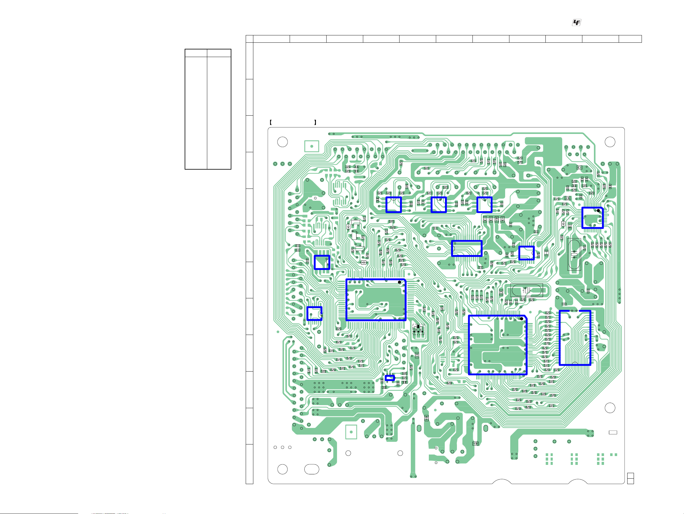
STR-KSL600
• Semiconductor
Location
Ref. No. Location
D1105 F-3
D1106 G-4
D1301 E-9
IC1111 J-4
IC1131 G-2
IC1301 E-10
IC1401 F-8
IC1403 E-7
IC1404 E-4
IC1405 E-6
IC1452 F-6
IC1501 I-7
IC1502 I-9
IC1601 H-4
IC1651 H-2
Q1103 F-3
Q1104 F-3
Q1105 E-3
5-4. PRINTED WIRING BOARD – DIGITAL Board (Component Side) – • See page 11 for Circuit Boards Location.
1 2 3 4 5 6 7 8 9 10 11
A
B
DIGITAL BOARD
C
D
E
F
C1122
C1123
G
H
I
J
K
(COMPONENT SIDE)
14
C1124
85
IC1131
71
IC1651
8
14
R1070
R1110
R1109
R1129
R1122
R1123
R1113
R1107
R1053
31
50
R1186
R1125
R1252
R1251
D1105
30
R1124
R1115
Q1105
Q1104
R1176
R1105
R1126
C1253
C1252
E
E
Q1103
D1106
R1098
R1177
E
IC1601
R1119
R1112
R1435
C1433
R1099
1
4
R1162
R1168
IC1111
R1128
C1108
R1433
IC1404
R1160
R1152
R1151
R1153
R1121
R1156
13
54
C1137
R1475
R1161
R1476
8
5
R1150
R1149
R1144
1
8051
R1473
C1473
R1143
100
81
R1106
R1127
R1189
C1107
R1423
X1101
R1436
R1425
R1041
FB1101
FB1502
R1463
1
C1423
4
IC1405
C1450
R1140
R1134
R1135
R1136
R1466
R1465
R1445
8
5
R1443
C1463
IC1403
28 15
1
C1443
4
IC1452
114
C1454
R1137
R1142
R1555
R1541
R1529
R1511
R1506
R1508
R1509
30 1
31
60
61
FB1501
R1485
FB1452
R1505
R1426
R1504
R1503
R1446
R1486
R1483
8
5
FB1405
FB1453
R1405
R1407
FB1503
R1502
IC1501
R1403
C1483
R1404
FB1406
C1408
R1523
R1542
R1527
R1406
C1522
R1536
C1405
C1407
R1408
C1521
90
8
R1515
R1537
R1493
R1492
C1404
1
169
IC1401
X1502
120
R1554
R1517
R1518
R1519
R1522
R1521
91
R1535
R1538
R1543
R1528
R1409
R1501
R1548
R1549
R1550
R1526
R1525
R1552
R1553
R1520
R1532
R1547
JR1020
R1539
R1305
R1306
D1301
C1303
R1309
44
R1533
R1534
R1540
R1544
R1307
C1913
R1551
R1304
FB1301
R1360
FB1305
IC1502
: Uses unleaded solder.
R1303
R1308
FB1302
C1302
13
C1304
R1301
C1305
C1301
R1302
R1362
C1131
R1361
112
48
IC1301
24
R1310
X1301
R1311
C1063
2223
1
3625
R1312
37
Z5
R1313
R1315
R1316
STR-KSL600
L
1-861-783-11(11)
1212
Page 13
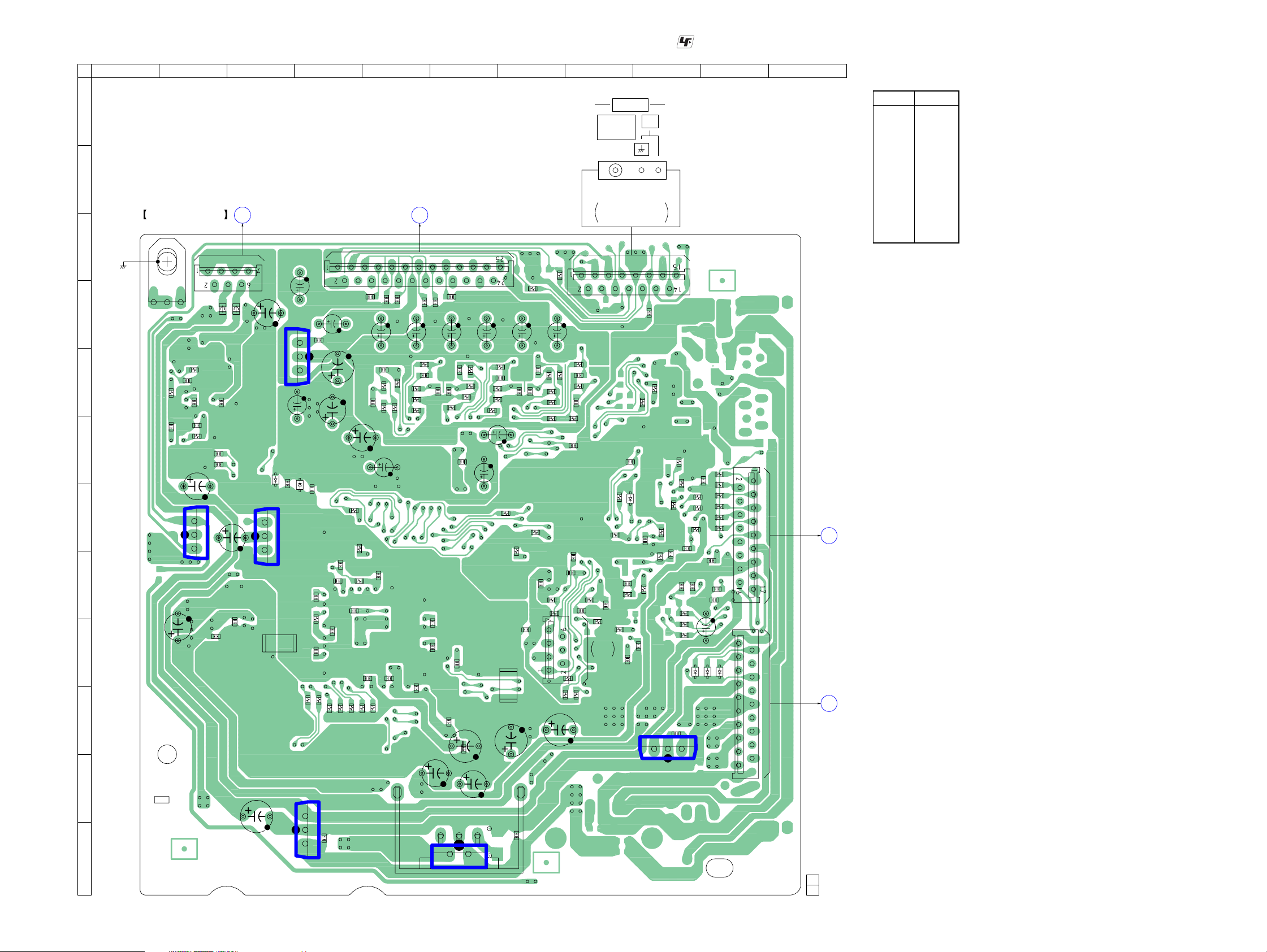
STR-KSL600
5-5. PRINTED WIRING BOARD – DIGITAL Board (Conductor Side) – • See page 11 for Circuit Boards Location.
1 2 3 4 5 6 7 8 9 10 11
A
B
R1480
CNS191
C1567
R1444
R1481
R1442
R1440
C1506
B
C1568
R1441
C1441
C1504
C1505
C1906
I/O BOARD
CNS403
C1569
C1418
C1442
R1460
C1516
IC1901
1
24
C1462
C1502
R1462
C1456
C1517
C1518
C1461
R1464
C1908
C1458
R1461
5
R1424
R1422
R1420
C1460
R1421
C1421
R1044
JR2001
C1455
C1515
R1049
C1905
C1428
C1422
C1299
C1138
R1261
C1471
R1043
C1472
R1470
R1430
CNS192
C1468
R1474
R1472
R1636
R1635
C1022
R1260
R1431
R1471
C1431
R1434
R1432
C1459
C1605
C1620
C1101
R1051
R1050
DIGITAL BOARD
(CONDUCTOR SIDE)
I/O BOARD
A
CNS301
(Page 18) (Page 18)
C
C1306
C1402
3
1
JR2002
C1491
C1401
C1002
D1004
1
3
C1004
C1001
C1403
D1003
C1003
C1511
C1501
C1510
R1514
C1513
R1545
R1546
R1574
IC1031
3
1
C1031
C1547 C1566
R1556
C1509
C1514
R1573
C1406
R1513
R1512
R1572
C1508
R1571
C1482
C1487
C1438 C1448
C1481
R1484
R1482
C1457
C1503
C1507
R1570
(CHASSIS)
G1101
D
R1318
E
R1317
C1313
F
C1064
G
C1315
R1314
C1314
3
1
C1312
C1309
C1310
CN197
FB1308
C1914
C1308
FB1309
IC1001
IC1902
IC1071
H
C1519
I
C1525
C1520
J
K
L
C1032
ANTENNA
FM 75Ω
COAXIAL
TUNER UNIT
SUPPLIED WITH THE
ASSEMBLED BLOCK
CNS195
C1432
C1126
R1178
R1097
C1121
R1039
R1190
R1052
CHECK
FOR
R1165
C1604
R1085
C1130
TN1
D1103
C1129
AM
C1251
R1169
R1167
C1142
R1193
R1166
IC1904
R1096
: Uses unleaded solder.
R1158
R1159
C1066
D1110
C1139
C1065
C1068
R1071
R1072
R1073
R1088
R1180
R1179
D1107
C1067
19
C1069
D1108
CNS194
1
R1083
C1125
C1021
R1082
R1175
R1058
R1059
R1081
C1100
C1120
13
R1201
CNS193
18
2
1-861-783-
• Semiconductor
Location
Ref. No. Location
D1003 G-4
D1004 F-3
D1103 G-8
D1107 I-10
D1108 I-10
D1110 I-9
IC1001 E-3
IC1031 L-4
IC1071 G-2
IC1901 L-6
IC1902 G-3
IC1904 J-9
D
DISPLAY
BOARD
CNS151
(Page 24)
C
MAIN
BOARD
CNS822
(Page 20)
11
(11)
STR-KSL600
1313
Page 14
STR-KSL600
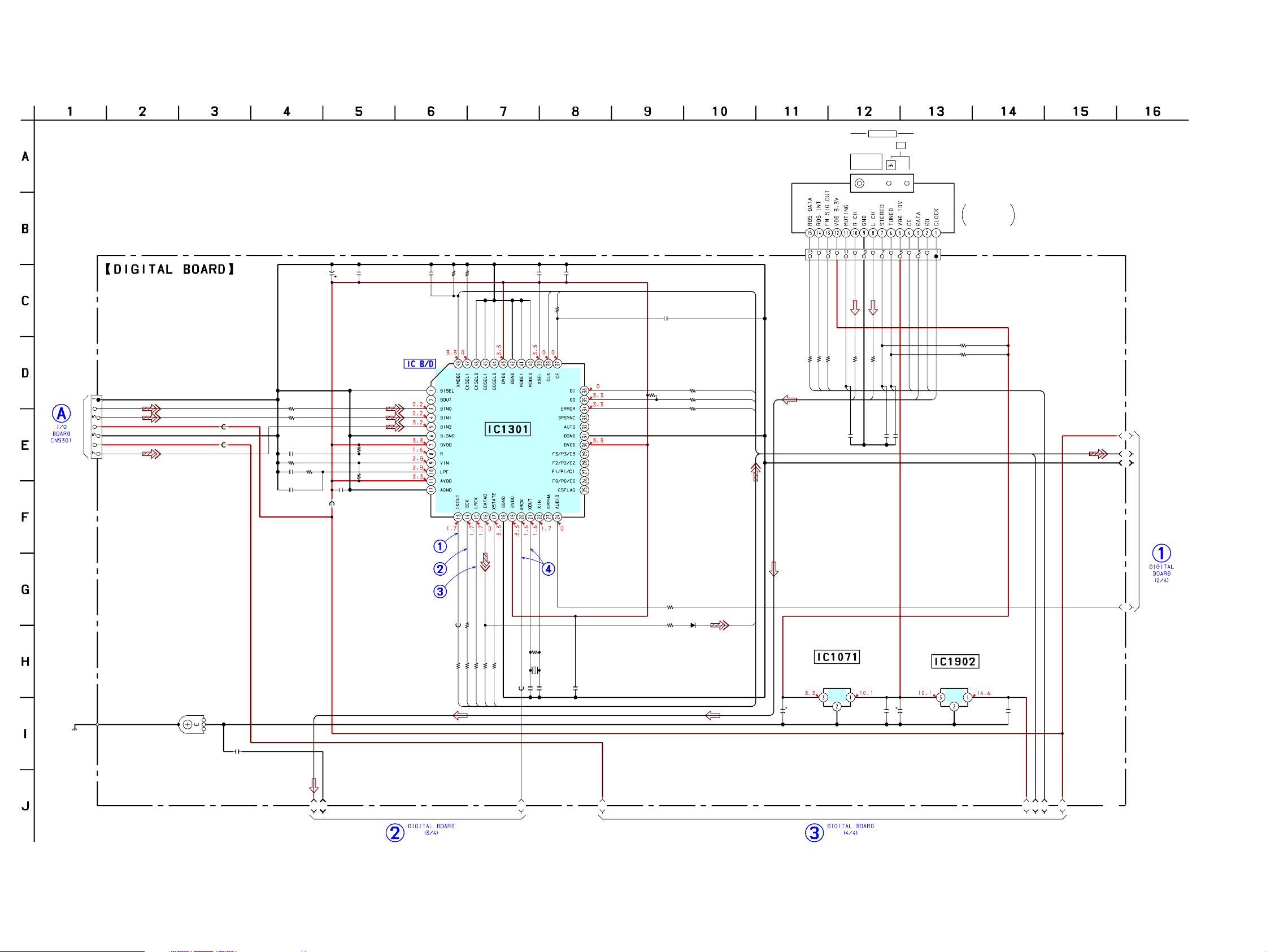
5-6. SCHEMATIC DIAGRAM – DIGITAL Board (1/4) –
(1/4)
CN197
7P
NC
(Page 19)
DVD-IN
TV-IN
+3.3V
GND
+5V
COAX-IN
FB1308
FB1309
R1362
R1361
R1303
C1303 R1304
0.1 100
C1304
0.01
• See page 26 for Waveforms. • See page 26 for IC Block Diagram.
C1302
FB1302
C1306
C1305
47
0.1
16V
100
100
0.01
33k
C1301
0.1
R1301
R1302
5.6k
4.7k
R1317R1318C1315 C1314 C1312
10k10k0.1 0.1 0.1
XMODE
DIGITAL AUDIO
INTERFACE RECEIVER
IC1301
LC89056W
CE
CLK
C1313R1316
R1314
ANTENNA
AM
FM 75Ω
COAXIAL
TN1
TUNER UNIT
SUPPLIED WITH
THE ASSEMBLED
BLOCK
CNS195
15P
100p100
0
MUTE
0.1
C1251
R1261
ROUT
0
R1260
LOUT
STRO
0.1
C1253
TUNED
0.1
C1252
R1252
39k
R1251
39k
LATCH
DO69
DAT19
CLK20
A1
A2
A3
100
100
100
1059
R
R1058
R1175
SIG
RDATA
R1315
100
R1313
10k
R1312
DI
100
DO
100
ERROR
RCLK
(CHASSIS)
STR-KSL600
G1101
C1131
R1311
R1308
100
D1301
100
1SS352
DATA
C1064
47
16V
+3.3V REGULATOR
IC1071
BA33
C1063
+10V REGULATOR
IC1902
7810
OGIOGI
C1914
47
0.1
16V 0.1
C1913
C5
C6
C7
C9
(Page 17)
100
1360
R
FB1301
0
22
100
1020
JR
BCKI2
R1306
LRCKI2
100
1307
1309
R
R
STAGE
SDI2
FB1305
R1310
1M
18p
X1301
12.288MHz
C1309
B3
C1308C1310
0.118p
1
C
470
1305
R
KFSIO
0.1
1
2
B
B
(Page 16)
(Page 15)
A4
1414
Page 15

STR-KSL600
5-7. SCHEMATIC DIAGRAM – DIGITAL Board (2/4) –
(2/4)
A1
A2
(Page 14)
A3
PM
R1501
A4
XRST
MCLK
LRCKI2
BCKI2
SDI1
LRCK
BICK
KFSIO
SDTI3
SDTI1
SDTI2
LRCKI2
BCKI2
SDI2
R1512
100
C1511
C1521 C1522
10p 10p
X1502
13.9MHz
R1515
1M
R1556
100
1k
0.1
FB1503
R1503
220
R1523
C1510C1509
0.10.1
220
R1513
R1502
100
R1504
100
R1505
100
R1506
100
• See page 26 for Waveforms. • See page 29 for IC Pin Function Description.
C1515
470
10V
1
A
0
2
D
A
SIGNAL PROCESSOR
0
A
10k
100
100
R1508
R1509
T
U
N
K
IN
C
A
D
H
H
2
O
L
S
1
C
D
C
P
H
H
H
G
1
2
D
D
AUDIO DIGITAL
IC1501
CXD9720BQ
0
0
E
S
C
W
C1513C1516 R1514
0.10.1 10k
3
4
5
6
7
3
4
5
6
7
D
D
D
D
D
A
A
8
A
A
A
A
R
O
R
R
E
FB1501
1
2
3
4
5
6
3
4
5
A
A
220
220
R1520
R1521
10k
R1574
10k
R1573
10k
R1572
10k
R1571
10k
R1570
A10
A11
A12
A9
D8
D9
D10
D11
D12
D13
D14
D15
A13
A14
C1507
C1501
C1504
C1506
0.1
0.1
0.1
0.1
A15
S-RAM
IC1502
IS61LV6416-EL10
R1511
100
C1503 C1505 C1508 C1502
0.1 0.1 0.1 0.1
220
R1528
4
1
A
220
R1527
5
1
A
3
1
A
7
A
220
R1522
220
220
R1544
R1545
8
A
C1514 C1518
D
D
D
220
220
220
R1519
R1518
R1517
220
220
220
220
220
R1546
R1555
R1543
R1542
R1540
0
3
4
5
1
1
1
S
7
D
D
D
C
A
C1525
100
0.1 0.1
10V
R1529
220
D
220
R1554
220
R1539
2
1
D
0.1
C1519
0.1
C1520
D
220
R1553
220
R1538
1
1
D
D
220
R1552
220
R1537
0
1
D
D
220
R1525
220
R1536
9
D
0
D
220
R1526
220
R1535
9
D
220
R1541
0
E
W
6
A
220
R1551
220
R1547
9
A
2
A
220
R1550
220
R1534
2
1
A
1
0
A
A
220
220
R1549
R1548
220
220
R1533
R1532
0
1
1
1
A
A
C1517
470
10V
GP9
A
STR-KSL600
E1
E2
(Page 16)
FB1502
D1
D2
(Page 17)
1515
Page 16

STR-KSL600
5-8. SCHEMATIC DIAGRAM – DIGITAL Board (3/4) –
(3/4)
10
50V
C1405
0.1
C1403
220
10V
R1492R1404
100k100k
R1403 R1493
100 100
CNS191
(Page 19)
25P
TUNER-L
GND
TUNER-R
R-OUT
GND
L-OUT
L-IN
GND
R-IN
GND
SL-IN
GND
SR-IN
GND
C-IN
+7V
SW-IN
-7V
DATA
CLOCK
LATCH
SW RELAY
VIDEO SW1
VIDEO SW2
VIDEO MUTE
LOUT
ROUT
DAT19
CLK20
SW-_RY
V_SW1
V_SW2
V_MUTE
R1486
1k
C1487
0.0022
C1547
0.0022
R1446
1k
C1567C1568
0.00220.0022
DAT19
CLK20
LAT
• See page 26 for Waveforms. • See page 26 for IC Block Diagrams.
(Page 14) (Page 15)
B1
B2
A/D CONVERTER
IC1401
AK5380
C1402
C1406
220
10V
C1404
10
0.1
50V10
R1482
4.7k
R1483 R1484
180 180
C1482
470p
C1483
470p
C1407
0.1
C1481
3300p
MIX AMP
IC1403
4565
VCC
R1476
C1566
0.0022
C1569 R1436
0.0022 1k
R1466
R1426
VEE
C1468
10
1k
50V
C1428
10 50V
C1458
10
50V
1k
C1418
10
50V
1k
C1491C1401
50V
R1485
4.7k
C1448
10
50V
C1438
10
50V
B3
R1406 R1405
1k 2.2k
C1441
0.0033
R1444
180
BCKI2
LRCKI2
SDI1
R1445 R1442
R1443
180
C1442
470p
C1443
470p
E1
R1408 R1409
10k 47k
4.7k 4.7k
R1472
C1472
R1407
C1408
C1471
4.7k
0.0033
R1474
R1473
180
470p
R1475
4.7k
C1473
100
0.1
FB1405
FB1406
180
470p
R1481
R1480
R1441
R1440
R1471
R1470
FB1453
C1454
E2
I
K
K
N
T
L
C
S
D
C
R
C
C
C
C1457
0.1
10
50V
4.7k
4.7k
4.7k
4.7k
4.7k
4.7k
MIX AMP
VEE
VCC
L
0.0033
R1430
C1431
R1434
K
K
I1
I2
I3
T
D
S
4.7k
180
L
T
T
IC
C
D
D
B
M
S
S
C1459
0.1
ISS367-T3
ISS367-T3
0.1
C1003
+5V REGULATOR
IC1001
7805
OGI
0.022
C1004
C1423
D1003
D1004
C1002
0.1
R1422
4.7k
C1421
0.0033
R1424
C1422
180
470p
R1423
180
R1425
4.7k
470p
F1
F2
F3
4.7k
R1461
R1432
C1432
4.7k
R1433
470p
D/A CONVERTER
IC1452
AK4355
4.7k
4.7k
4.7k
R1460
R1421
R1420
4.7k
R1431
180
C1433
4.7k
R1435
470p
C1455 C1460
C1456 C1450
0.1 0.1
R1462
4.7k
C1462
470p
R1465
10
50V1050V
C1461
0.0033
R1464
180
180
R1463
4.7k
C1463
470p
FB1452
VCC
MIX AMP
IC1405IC1404
45654565
C1001
470
10V
VEE
(Page 17)
F4
F5
STR-KSL600
1616
Page 17

STR-KSL600
5-9. SCHEMATIC DIAGRAM – DIGITAL Board (4/4) –
(4/4)
C5
C9
C1
C7
R1189
10k
GENERATOR
IC1111
10k
X1101
16.5MHz
R1041
R1140
R1134
R1135
R1136
R1137
R1099
R1085
10k
C1137
0.01
CD NC
GVO
100
100
100
100
100
100
10k
D1103
1SS352
R1176
10k
(Page 14)
(Page 16)
R1127
100
RESET SIGNAL
S-80929ANM
C1138
0.1
R1049
10k
C1299
0.1
R1043
C6
F1
F2
F3
F4
F5
10k
XMODE
CLK
CE
DI
DO
ERROR
STAGE
DATA
R1178
• See page 26 for Waveform. • See page 29 for IC Pin Function Description.
E
O
A
0
SS
X
V
X0
X1
VCC3
NOT IN USE
NC
NOT IN USE
LRCK_SW
NOT IN USE
NOT IN USE
NOT IN USE
NOT IN USE
XMODE
CKSEL1
CLK
CE
DI
DO
ERROR
E
O
A
AT
T
T
A
D
XS
100
R1044
A
X1
9
P
G
100
R1142
9
P
G
R1177
10k
2SC2712-YG
MUTING
SWITCH
Y
-R
P
100
R1106
100
R1143
A
Q1104
9
Y
N
K
L
-O
F
-C
F
10k
10k
R1051
R1050
X
Y
N
LA
ST
_O
E
R
N
A
R
F
ER
W
O
P
N
T
AC
CS
H
BS
H
100
100
R1149
R1144
T
N
S
C
S
A
C
R
X
H
H
Y
T
-C
F
100
R1053
LK
_C
N
FA
ST
R
X
100
R1150
M
P
Y
6
-R
O
-R
-R
F
C
R
D
4.7k
R1110
R1039 C1100
10k 0.1
4.7k
4.7k
100
1k
R1107
R1109
R1052
R1125
Y
Y
L2
L1
A
A
AY
R
EL
EL
EL
T
TR
C
R
R
R
T
E
F_C
F_
N
AR
TR
E
O
N
R
FR
CE
N
N
S
D
_C
_P
0
55
38
12
43
5
S
P
M
S
AK
AK
G
P
V
100
100
R1151
R1121
2
1
N
P
S
G
C
Q1103
RT1N141C-T
MUTING
SWITCH
H
R
C
P
T
A
L
100
R1112
1k
R1126
O
R
CH
D
O
T
CT
LA
S
TE
O
R
P
SYSTEM CONTROLLER
MB90478PF-G-177
T
N
D
LK
D
_C
_C
_P
55
55
355
43
43
4
K
A
AK
AK
100
100
R1153
R1152
I
K
T
L
D
C
C
C
R1156
100
D
E
N
U
T
0.1
C1101
1k
R1119
IC1601
-BNDE1
0
2
K
L
C
O
T
R
U
T
M
S
2
B
1
6
T
6
K
S
IN
L
L
F
C
D
100
100
100
100
R1122
R1115
R1113
R1123
)
IN
D
L(A
O
V
CRYSTAL SEL
E
T
K
U
CL
F.M
H
100
100
R1160
R1169
K
L
C
H
T
A
L
D1106 D1105
1SS352 1SS352
E
D
S
O
(B)
L
S
U
O
C
V
IN
T
O
N
MD1
MD0
STOP
T
D
2
2
1/SW
-SW
H
H
O
S
E
VID
FLA
FLAS
IG
H
/D
5
C
A
C
AT
L
AN
VC
1
W
S
_
V
E
K
O
T
TB
L
ED
E
U
C
N
_S
ER
U
M
T
T
FL
S
Y
A
EL
R
T
FER
U
A
O
IN
O
T
K
O
D
D
A
W
H
H
CL
D
100
100
R1161
R1162
Y
T
R
U
-_
IN
O
D
D
W
S
H
H
R1167R1168
100100
9
1
T
A
D
K
A
L
T
A
C
D
R
R
C1108 R1128R1201
0.1 10022k
S
MD2
TA
LK
CT
EY
C
A
R1096
R1098
C
IR
TE
D
S
E
S
S
D
D
R
E D
R
S
FU
NC
VERSION
MODEL
RDS SIGNAL
VSS
A/D3
A/D2
A/D1
EN
A/D0
SC
X
AVSS
AVRH
AVCC
SDA
SCL
VIDEO-MUTE
XRST
10k
10k
R1082
R1081
1
2
H
H
S
S
A
A
2
L
W
F
FL
S
_
V
10k
10k
Q1105
2SC2712-YG
MUTING
SWITCH
C1126
220p
K
ER
W
PO
K
CL
S
1
W
-S
EO
ID
V
P
O
T
S
C1107
0.1
R1190
10k
10k
R1083
E
T
U
M
_
V
C1139 C1142
0.1 0.1
IG
S
0.1
0.01
0.01
C1605
C1130
C1129
R1166
10k
R1165
0
0.01
C1125
C1120
C1604
0.1
3.3k
R1159
R1129 100
R1186
R1105
R1124
10k
R1636
C1620
0.1
0.1
R1070
3.3k
10k
R1158
R1071
EEPROM
IC1131
BR24L16
R1193
(Page 15)
C1065
C1066
D2
C1905
F-RY
C-RY
R-RY
F-ON
F-CT
PRO
F-CLK
0.1
-27V
F2
F1
STOP
P-RY
F1
-27V
F2
D1110
ISS352
D1107
1SS352
1SS352
D1108
VO2 VI
VC VO1
+3.3V REGULATOR
C1021
0.1
LEVEL SHIFT
G
220p
220p
IC1651
TC74VHCT08AFT
+3.3V/+2.6V
REGULATOR
G
IC1901
SI-3004KWF
47 16V
C1906
47 16V
C1908
IC1904
BA33
OI
G
C1022
470
10V
CNS194
FRONT SP RELAY
CENTER SP RELAY
REAR SP RELAY
FAN_ON/OFF
F_CTRL2
PROTECTOR
F_CLK
STANBY+V
DIGITAL+V
STOP
POWER RELAY
FUNCTION_MUTE
CNS193
+3.3V(STBY)
FL LAT
FL CLK
FL DATA
VOL UP
VOL DOWN
POWER SW
SIRCS
CNS192
RESET
FLASH2
FLASH1
19P
+V
GND
GND
GND
-27V
F2
(Page 23)
F1
17P
F1
-27V
F2
GND
GND
+5V
(Page 25)
AD2
AD1
AD0
7P
MD2
MD0
GND
(FOR CHECK)
VDD
D1
+5V REGULATOR
IC1031
BA05T
OI
G
FLSTB
10k
R1088
C1069
C1068
10k
R1180
C1032
470
10V
10k
R1179
10 50V
0.1
C1067
220p
V
2
1
6
6
K
IN
L
C
D
C1031
0.1
RESET
10k
10k
100
MD2
MD0
R1635
10k
0.1
C1121
0
10k
0.1
10k
R1072
10k
R1073
0.1
C1122
0.1
C1123
FB1101
C1124
R1097
MD2
MD0
RESET
FLASH2
FLASH1
100k
STR-KSL600
1717
Page 18

STR-KSL600
• Semiconductor
Location
Ref. No. Location
D301 C-1
D405 C-6
IC201 D-5
IC301 B-2
IC302 B-2
IC303 C-2
IC401 D-3
IC402 D-4
IC403 E-5
IC404 E-5
Q401 E-4
Q402 C-6
5-10. PRINTED WIRING BOARD – I/O Board – • See page 11 for Circuit Boards Location.
1 2 3 4 5 6
A
B
C
D
I/O BOARD
C301
C308
JW262
JW881
D301
C309
JW263
JW883
JWH02
JW844
C311
C310
JW880
JW837
JW835
CNS301
TV/SAT
OPT IN
IC301
C414
C419
JW836
JW833
JW834
IC301
C312
C417
C416
R307
R306
IC303
14 8
JW826
17
C433
JW870
C415
C490
JW832
C489
R481
C497
R482
JW861
R483
C487
DIGITAL
C418
24
25
C467
C302
C488
R430
C495
OPT IN
IC302
C307
R305
C413
R410
IC302
DVD
1313
R304
IC401
40 41
C485
JW840
C306
R303
C305
1
80
C493
J301
DVD
COAX IN
C304
R451
C483
CNS403
C496
C303
65
64
C491
C481
(CHASSIS)
R453
JW845
C464
JW843
C484
C486
JW829
JW830
E
CC51
C465
E
: Uses unleaded solder.
AUDIO IN
TV/SAT R
DVD R
VIDEO R
CC52
CC53
R452
JW860
JW846
C492
R376
Q401
JW819
C482
JW890
C472
C494
R475
JW891
JW822
R560
JW818
R471
R472
R499
TV/SAT L
R403
JW817
JW831
C443
DVD L
VIDEO L
CC03
JW821
R473
C498
R474
IC402
JW816
C466
C442
J501
CC02
JW820
C471
JW815
R401
85
14
JW814
CC01
C206
C441
MONITOR
OUT
DVD
VIDEO
R203
R484
R470
JW838
C207
JW811
JW813
3
IC404
VIDEO IN
C204
R402
R204
JW827
JW828
IC201
JW839
L201
JW812
C440
13
R202
C209
JW810
IC403
1
CN404
SUB WOOFER
C210
C202
C203
JW809
148
1
J403
OUT
R476
17
C208
RY401
JWH01
L202
JW801
JW807
JW806
JW805
JW862
(CHASSIS)(CHASSIS)
R480
JW808
E
Q402
R477
CNS401
1-861-782-
10
C400
D405
R479
E
MAIN
BOARD
CNS402
(Page 20)
F
11
(11)
MAIN BOARD
CNP821
(Page 20)
STR-KSL600
DIGITAL BOARD
A
CN197
(Page 13) (Page 13)
DIGITAL BOARD
B
CNS191
1818
Page 19

5-11. SCHEMATIC DIAGRAM – I/O Board – • See page 26 for IC Block Diagrams.
IN301
TV/SAT
AUDIO IN
VIDEO IN
DIGITAL
COAX IN
TV/SAT L
VIDEO L
TV/SAT R
VIDEO R
MONITOR
SUB WOOFER
OUT
DVD L
DVD R
VIDEO
OPT IN
IN302
DVD
OPT IN
J301
1P
DVD
(CHASSIS)
J501
9P
OUT
DVD
J403
1P
(CHASSIS)
IC301
TORX141
DIGITAL OPTICAL
RECEIVER
IC302
TORX141
DIGITAL OPTICAL
RECEIVER
2200p
C464
0.1
R403CC03
1k100P
CC53 R453
100P 1k
R402
CC02
1k
100P
R452
CC52
1k
100P
R401CC01
1k100P
R451
CC51
1k
100P
R480 R484
47k 100k
RY401
R476
1k
R477
1
V
2
V
Q402
2SC2785
RELAY
DRIVE
4.7k
C413 C433
2.2
2.2
50V
50V
Y
L
-R
-R
-L
W
U
U
T
T
S
1
C
V
N
5
N
O
M
+
M
2
T
D
U
2
N
O
V
M
G
VIDEO
1
D
AMP & SWITCH
N
G
IC201
NJM2279
D405
1SS133
C400
0.1
C210
R479
100
R204
75
C203
10
50V
2
V
W
-5
S
C204R203
47p75
1
W
3
S
V
STR-KSL600
NC
DVD-IN
0.1
C301
560k
R306
R304
1k
C305
22
50V
R303
75
C304 C303
0.1 1000p
C465
220
10V
C491
4.7
50V
AUDIO SELECTOR,
ELECTRICAL VOLUME
C207
C206 C208
470
0.1 0.1
6.3V
IC401
M61527FP
T
U
-O
L
L201 10µH
C492
4.7
50V
R430R410
47k47k
T
U
-O
R
L202
10µH
C209
470
6.3V
C306
0.1
4.7 50V
C482
4.7 50V
C483C481
4.7
4.7
50V
50V
50V
50V
50V
2.2
2.2
2.2 50V
2.2
C414
C415
C417
C416
-IN
-IN
-IN
R
L
-IN
L
R
S
S
R560
10k
C484
4.7 50V
C494
C493
4.7
50V
C485
4.7
50V
C495
4.7
50V
100
50V
2.2
C418
-IN
C
LINE AMP
IC402
NJM4565
VCC
VEE
100
R481
R482
C419
2.2
50V
A
-IN
T
K
A
W
L
S
D
C
INVERTER
TC74HCU04AF
C308
C490
100p
C489
100p
C497
100p
100
R483
T
A
L
R474
2.2k
R499
47k
C311
10
50V
D301C307R305C302
1SS1331p22k0.1
R307
100
C312 C309
C310
470
IC303
6.3V
47p
C486
4.7
50V
C496
4.7
50V
C498
33p
R376
1k
2SC3576
REGULATOR
C467
0.1
C471
4.7
50V
R470
47k
R473
2.2k
470
0.1
6.3V
TU-L
TU-R
R-OUT
R472
1k
R471
680
Q401
+3.3V
10V
50V
10
0.1
220
2.2k
C487
C488
C466
R475
C472
4.7
50V
L-OUT
L-IN
R-IN
SL-IN
SR-IN
C-IN
SW-IN
DATA
CLK
LAT
SW-RLY
C442
C443
100
10V
100
10V
+7V REGULATOR
IC403
78M07
OGI
OGI
IC404
79M07
C440
0.1
C441
0.1
TV-IN
+3.3V
GND
COAX-IN
CNS301
CNS401
11P
L-CH
GND
R-CH
GND
C-CH
GND
SW-CH
GND
SL-CH
GND
SR-CH
CNS403
25P
TUNER-L
GND
TUNER-R
R-OUT
GND
L-OUT
GND
R-IN
GND
SL-IN
GND
SR-IN
GND
SW-IN
DATA
CLOCK
LATCH
SW RELAY
VIDEO SW1
VIDEO SW2
VIDEO MUTE
CN404
CHASSIS GND
CHASSIS GND
AUDIO+
AUDIO-
R2 GND(RELAY)
VIDEO GND
+5V
(Page 14)
7P
(CHASSIS)
(Page 22)
L-IN
C-IN
+7V
(Page 16)
-7V
10P
+7V
-7V
+5V
(Page 23)
-5V
STR-KSL600
-7V REGULATOR
C202R202
10
75
50V
The components identified by mark 0 or dotted
line with mark 0 are critical for safety.
1919
Replace only with part number specified.
Page 20

STR-KSL600
5-12. PRINTED WIRING BOARD – MAIN Board –
1 2 3 4 5 6 7 8 9 10 11 12 13
+
+
+
+
+–
MAIN BOARD
R791
C791
C641
JW166
R641
C643
C744
JW167
C544
R741
C644
C794
C642
C694
R643
C511
C741
R642
JW168
C518
JW169
JW172
JW132
C507
R509
C508
R515
JW170
C510
TM601
A
B
SPEAKERS
IMPEDANCE USE 6 – 16Ω
L
–
FRONT
–
R
CENTER
–
L
–
SURR
R
C
(CHASSIS)
D
• See page 11 for Circuit Boards Location. : Uses unleaded solder.
(Page 21)
STBY BOARD
K
CNP903
41
CN820
JW174
RY501
-1 -2
JW173
C506
R505
JW171
JW233
111
210
L507
R507
C504
D520
E
Q520
R522
R508
R504
R503
C503
RY601
-1 -2
R510
R367
R501
IC501
C502
C501
C509
R502
R375
R540
E
R368
R622
D620
Q363
R640
E
D521
JW175
R379
C373
R740
Q620
D621
D720
E
E
Q720
JW179
C374
Q364
JW181
JW180
-1 -2
R366
RY701
JW176
JW177
C732
JW178
JW141
E
R750
Q732
R730
D731
R722
JW182
R732
R610
JW187
C611
C618
JW184
R733
R731
C730
Q731
E
Q730
E
D721
R710
JW183
R608
JW188
R609
C606
C607
C608
C610
R615 C601
JW186
JW185
R607
JW232
JW189
111
210
L607
IC601
C818
JW190
R605
R660
C603
C604
R603
R604
C602
R601
R760
R602
C609
JW197
JWH03
JW841
JW193
R371
R377
JW194
E
Q365
C375
R369
JW259
C819
JW198
JW230JW231
JW196
JW261
JW200
JW199
JW201
JW202
JW159
JW158
1
JW241
4
JW228
JW204
D809
JW203
JW205
C661
JW252
C801
C802
JW240
JW227
R658
C668
R659
(Page 21) (Page 21) (Page 21)
T901
G
JW251
JW250
C820
D812
C657
C656
C660
R832
JW842
R665
D813
JW209
C658
D810
R831
C821
D811
JW210
JW207
JW208
JW206
JW234
111
210
R657
JW229
R655
CNP801
L657
C814
JW211
C653
13
D803
C654
IC651
1
C812
R653
H
CNP804
R372
R654
C652
R652
C651
R651
E
R810
Q366
T901
3
R378
R811
JW214
C659
R380
C811
C376
D802
R370
C813
JW213
T901
J
1
D801
JW216
CNP802
D804
JW218
JW212
R910
JW219
JW215
D815
C805
D816
5
C804
JW220
C803
JW222
JW221
JW224
JW120
D805
D817
JW223
C806
D814
R558
D806
R556
C561
C815
C562
R554
JW226
JW217
E
R557
Q550
C817
C816
R555
R553
E
C565
D807
D808
R552
D550
C563
Q551
R551
C564
JW137
JW135
JW136
JW134
IC751
10 2
R751
11 1
C753
R754
JW103
R755
C754
R753
IC751 F-5
Q361 F-9
Q362 F-4
Q363 D-5
Q364 D-5
Q365 D-8
Q366 C-11
Q379 G-9
Q520 B-4
Q550 C-12
C755
JW139
R765
C760
C758
C757
C756
Q551 C-13
Q620 B-5
Q720 B-5
Q730 B-6
Q731 B-6
Q732 B-6
Q861 F-2
Q862 G-2
Q863 F-2
Q866 G-2
C768
JW105
JW104
L757
JW144
JW142
JW143
JW140
C761
R759
JW106
R757
R758
JW107
JW111
JW146
JW253
CNP821
F
JW149
JW147
JW109
JW108
I/O BOARD
CN404
(Page 18)
JW148
JW155
JW150
110
JW151
JW152
JW112
JW153
JW254
JW113
JW117
C446
IC405
3
JW154
JW115
C444
JW116
C447
1
E
R373
R363
Q361
JW157
C701
C445
IC406
JW160
10 2
R701
R702
11 1
C703
R703
C702
C371
R704
C709
R361
R381
13
E
Q379
IC701
R705
R708
C704
JW118
C705
JW162
R715
C710
C708
C707
C706
JW258
JW257
JW119
JW256
R885
JW235JW236
R707
R709
L707
C718
JW165
C711
JW122
JW243
JW121
JW114
CNS822
1
2
JW242
C
JW123
19
18
DIGITAL BOARD
CNS194
JW130
JW255
JW260
JW129
JW126
JW124
JW131
JW125
JW128
JW127
1-861-780-
11
(11)
(Page 13)
Q362
E
JW102
JW133
C751
R752
C752
R360
C759
E
Q861
D820
R881
Q862
CNP861
1
YEL
B
C
Q
R882
C871
R883
3
BLK
RED
M
M1
(FAN)
F
JW161
R884
E
Q863
E
E
Q866
G
R362
CNS402
E
R374
I/O BOARD
CNS401
(Page 18)
C372
• Semiconductor Location
D520 B-4
D521 C-5
D550 C-13
D620 B-5
D621 C-5
D720 B-5
D721 B-6
D731 B-6
D801 B-11
D802 B-11
D803 B-10
Ref. No. LocationRef. No. Location
D804 B-11
D805 A-12
D806 B-12
D807 B-13
D808 B-13
D809 B-9
D810 B-10
D811 B-10
D812 B-9
D813 B-10
D814 B-12
Ref. No. Location Ref. No. Location Ref. No. Location
D815 B-11
D816 B-12
D817 B-12
D820 F-2
IC405 G-8
IC406 G-9
IC501 D-4
IC601 D-7
IC651 D-10
IC701 F-9
STR-KSL600
2020
Page 21

STR-KSL600
5-13. PRINTED WIRING BOARD – STBY Board –
1 2 3 4 5 6 7
A
B
• See page 11 for Circuit Boards Location. : Uses unleaded solder.
STBY BOARD
C925
C923
G102
D954
D955
D952
D953
C922
C921
T902
SUB POWER
TRANSFORMER
2
CNP901
1
R953
(AC IN)
D951
C
D
G
MAIN BOARD
CNP801
(Page 20)
H
MAIN BOARD
CNP804
(Page 20)
J
MAIN BOARD
CNP802
(Page 20)
T901
MAIN POWER
TRANSFORMER
(CHASSIS)
K
MAIN
BOARD
CN820
(Page 20)
CNP903
4
1
R951
R952
Q951
Q901
E
JW950
D956
D957
E
C924
R956
R955
R954
CNP902
12
FH901
F901
RY901
FH902
1-861-781-
11
(11)
• Semiconductor
Location
Ref. No. Location
D951 B-6
D952 B-3
D953 B-3
D954 A-3
D955 B-3
D956 B-4
D957 B-4
Q901 C-3
Q951 B-3
STR-KSL600
2121
Page 22

STR-KSL600
5-14. SCHEMATIC DIAGRAM – MAIN Section (1/2) –
(1/2)
(Page 19)
L-CH
R-CH
C-CH
SW-CH
SL-CH
SR-CH
POWER AMP
IC701
LM3886T
C706
R373
1k
R363
CNS402
11P
GND
GND
GND
GND
GND
100k
R360
100k
R374
1k
R375
1k
R367
100k
R368
47k
R377
1k
R371
100k
Q361
2SC3576
MUTING
Q362
2SC3576
MUTING
Q363
2SC3576
MUTING
Q364
2SC3576
MUTING
Q365
2SC3576
MUTING
0.022
0.022
0.022
C374
0.022
R361
4.7k
C371
C372
R362
4.7k
R379
4.7k
C373
0.1
R366
10k
R369
4.7k
C375
R701C701
1004.7
50V
R702C702
22k100p
POWER AMP
IC751
LM3886T
C756
C751
50V
R751
100
V+ NC NC NCMUTEGNDV+V-
C708
C707
1
0.1
50V
C757 R753
1
0.1 270
50V4.7
R752C752
22k100p
C710
1
0.1
50V
V+ NC NC NCMUTEGNDV+V-
C758
C760
1
0.1
50V
R705
22k
C704 R715
27p 33k
R703
270
R704
470
C709
100
10V
R755
22k
C754
R765 C768
27p
33k 1 50V
R754
470
C759
100
10V
C705
2200p
1000p
1000p
C703
C718
1 50V
POWER AMP
IC601
LM3886T
C753
C601
4.7
R601
50V
100
C755
2200p
R602C602
22k100p
C606
50V
1
V+ NC NC NCMUTEGNDV+V-
C608
C607
1
0.1
50V
R605
22k
R615C604
33k4.7p
C610 R603
0.1 270
C603
560p
C618
1 50V
R604
560
C609
100
10V
Z1
Z2
Z3
Z4
Z5
Z6
(Page 23)
STR-KSL600
C376
R372
100k
R378
1k
Q366
2SC3576
MUTING
0.022
R370
4.7k
POWER AMP
IC501
LM3886T
C501
4.7
50V
R501
100
C502
100p
R502
22k
BN1F4M
MUTING
CONTROL
SWITCH
C507 C510
1
0.1 0.1
50V
Q379
V+ NC NC NCMUTEGNDV+V-
C508C506
1
50V
R380
100k
R381
10k
R505
22k
R515
C504
33k
4.7p
C503
560p
C518
1 50V
R503
270
R504
560
C509
100
10V
POWER AMP
IC651
LM3886T
C651
4.7
R651
50V
100
R652C652
22k100p
C656
50V
1
V+ NC NC NCMUTEGNDV+V-
C658
C657
1
0.1
50V
R655
22k
R665C654
33k4.7p
C660 R653
0.1 270
C653
560p
C668
1 50V
R654
560
C659
100
10V
Z7
Z8
Z9
Z10
Z11
2222
Page 23

5-15. SCHEMATIC DIAGRAM – MAIN Section (2/2) –
STR-KSL600
(Page 22)
(Page 19)
Z1
Z2
Z3
Z4
Z5
Z6
Z7
Z8
Z9
Z10
Z11
CNP821
+7V
-7V
CHASSIS GND
CHASSIS GND
AUDIO +
AUDIO -
R2 GND(RELAY)
+5V
VIDEO GND
-5V
STR-KSL600
D809
(2/2)
L707
R707
4.7
R709
10
R708
47k
R758
47k
L757
R757
4.7
L507
R507
4.7 27k
L607
R607
4.7
L657
R657
4.7
R710
27k
R760
27k
R510
R508
47k
R610
27k
R660
27k
C561
4.7
50V
R558 R556 R554
100k 68k 820
C446
10
50V
C447
47
25V
C711
0.022
C761
0.022
R759
10
R509
10
C511
0.022
R608
47k
R658
47k
R609
10
C611
0.022
C661
0.022
R659
10
10P
-1
-2
RY701
D720
1SS133T
R740
47
Q720
2SC2785
RELAY
DRIVE
R733
47k
Q731 Q730
2SA988 2SC2785
R731
10k
C732 R732 Q732
0.1 33k 2SC1841
R750
1k
R540
47
Q520
2SC2785
RELAY DRIVE
RY601
R640
47
D620
1SS133T
Q550
2SC2785
+5V REGULATOR
IC405
7805
OGI
OGI
IC406
79M05
-5V REGULATOR
C730
220
10V
Q730-732
AC POWER
PROTECTOR
RY501
D520
1SS133T
-1
-2
C565
100
16V
R555R557
4.7k220k
R741
C741
4.7
0.01
R791
C791
4.7
Q551
2SC2785
0.01
R641
C641
4.7
0.01
R642
C642
4.7
0.01
C643
R643
0.01
4.7
C564
R551
4.7
100k
50V
R722
4.7k
F.R Y
D731
D721
1SS133T
1SS133T
R730
6.8k
-1
-2
D521
1SS133T
R522
4.7k
C.RY
D621
1SS133T
R622
4.7k
Q550,551
S.RY
D550R553
1SS133T10k
C563
R552
1
3.3k
50V
C444
0.1
C445
0.1
2SC2785
C562
50V
Q620
1
FAN MOTOR
LEVEL DETECT
RBV-602
2
14
C818
4700
50V
C819
4700
50V
C811
1000
25V
C812
1000
25V
C806
1000
25V
C805
1000
25V
C817
3300
16V
D802
10EDB40
D803
10EDB40
Q861
2SB734
D815
10EDB40
D816
10EDB40
C871
100
16V
3
R832 D812 D810
22k HZS30-1L 10EDB40
D801
10EDB40
D804
10EDB40
C813
1000p
C814
1000p
D814
10EDB40
D817 C803
10EDB40 1000p
D805
10EDB40
D808
10EDB40
R883
2.2k
R882
Q862
3.3k
BN1F4M
R881
1.5k
D820
RD5.6
Q861-863
FAN MOTOR DRIVE
S.RY
C.RY
F.R Y
R831
220
D813
HZ6.8BP
10EDB40 0.1
R884
47k
C801
0.22
C802
0.22
C820
100
50V
10EDB40
C804
1000p
D806 C815
R810
0.47
C821D811
220
35V
C816D807
0.110EDB40
Q863
BN1F4M
R910
0.47
BN1F4M
FAN MOTOR
DETECT
R811
0.47
F1
F2-30V
Q866
F1
F2
-30V
R885
100
CNP801
3P
+B
-B
CNP804
3P
+R2
-R2
CNP802
5P
+R3
-R3
C744
390p
C794
330p
C544
330p
330p
C644
330p
C694
CNP861
CNS822
CN820
19P
3P
4P
(CHASSIS)
M1
(FAN)
(CHASSIS)
CNP903 R956
FUNCTION MUTE
POWER RELAY
STOP
F1
DIGITAL+V
F2
STANBY+V
-27V
GND
GND
GND
F_CLK
+V
PROTECTOR
F_CTRL2
FAN_ON/OFF
REAR SP RELAY
CENTER SP RELAY
FRONT SP RELAY
TM601
SPEAKER
IMPEDANCE
USE 6–16Ω
G102
C925
0.1
4P 10k
(Page 17)
R952
4.7k
R951
47k
Q901
2SC2785
AC POWER
DETECT
T901
MAIN POWER
TRANSFORMER
C924
1
50V
Q951
2SC2785
RELAY DRIVE
C923
1000
25V
R955
33k
R954
47k
D952
10EDB40
D953
10EDB40
D954
10EDB40
D955
10EDB40
D956
1SS133T
D957
1SS133T
1SS133T
R953
F901
T1.6AL
250V
D951
1
C922
0.022
T902
SUB POWER
TRANSFORMER
C921
0.022
RY901
CNP902
CNP901
2P
2P
(AC IN)
The components identified by mark 0 or dotted
line with mark 0 are critical for safety.
2323
Replace only with part number specified.
Page 24

STR-KSL600
5-16. PRINTED WIRING BOARDS – PANEL Section –
1 2 3 4 5 6 7 8 9
DISPLAY BOARD
S123
A
1
1541
JW109
B
C
VOLUME BOARD
• See page 11 for Circuit Boards Location. : Uses unleaded solder.
C157
C158
FL101
12
11
IC152
JW118
C142
R178
JW117
C156
JW116
C155
JW115
C143
JW114
JW105
JW113
JW107
C141
JW112
JW111
JW110
23
22
33
34
144
C159
FLUORESCENT INDICATOR TUBE
JW108
10
DIGITAL BOARD
D
CNS193
CNS151
JW101
(Page 13)
D154
TUNERTV/SAT
1
1-861-778-
11
(11)
R198
6865644934
13
IC102
JW104
JW125
S117 – 123
C112
R153
R152
D151
VIDEO
JW120
JW121
JW123
JW124
D152
DVD
R199
JW102
D153
R176
CNP161
6
(CHASSIS)
D
• Semiconductor
Location
Ref. No. Location
D151 B-8
D152 B-9
D153 B-10
D154 B-10
IC102 B-8
IC152 B-4
LP101
RV101
ROTARY ENCODER
MASTER VOLUME
C160
1
3
S122
INPUT SELECTOR
S118
MUTING
R191
S117
SOUND FIELD
R192
S119
PL
R194
PRESET TUNING
CN160
1
S120S121
–+
6
1-861-779-
11
(11)
STR-KSL600
2424
Page 25

STR-KSL600
5-17. SCHEMATIC DIAGRAM – PANEL Section –
R199
1
REMOTE CONTROL
RECEIVER
IC102
RPM7240-H9
• See page 26 for Waveform. • See page 26 for IC Block Diagram.
FL101
FLUORESCENT INDICATOR TUBE
0
1
2
3
5
1
14
1
16
G
G
G
G
E
E
E
E
S
S
S
S
9
1
1
1
G
G
EG
E
E
EG
S
S
S
S
5
6
7
8
G
G
G
G
E
E
E
E
S
S
S
S
1
2
3
4
G
G
G
G
E
E
E
E
S
S
S
S
0
1
2
3
4
5
1
1
1
G
G
G
E
E
E
S
S
S
6
1
1
1
1
G
G
G
G
E
E
E
E
S
S
S
S
0
1
2
1
1
1
ID
ID
ID
R
R
R
G
G
G
0
1
2
9
1
1
1
ID
ID
ID
ID
R
R
R
R
G
G
G
G
5
6
7
8
ID
ID
ID
ID
R
R
R
R
G
G
G
G
1
2
3
4
ID
ID
ID
ID
R
R
R
R
G
G
G
G
C157
C158
R198
1
10
50V
0.1
(CHASSIS)
LP101
ROTARY ENCODER
MASTER VOLUME
C160
0.1
RV101
S119
MUTING
UT
GND
VO
VCC
R153
100
R152
10
C112
47
16V
R192
1k
PL
INPUT SELECTOR
R191
1k
SOUND FIELD
R194
1k
S122
S117S118
SEG9
SEG8
SEG7
SEG6
SEG5
SEG4
SEG3
SEG2
SEG1
C141
10
50V
C142
0.1
CN160 CNP161
6P 6P
GND
FLUORESCENT
INDICATOR TUBE DRIVER,
LED DRIVER
IC152
PT6315
1000p
220p
220p
C143
C155
C156
S123
GRID9
GRID8
GRID7
GRID6
GRID5
GRID4
GRID3
GRID2
GRID1
VIDEO DVD TV/SAT TUNER
R176
150
CNS151
17P
+3.3V(STBY)
FL DATA
VOL UP
VOL DOWN
POWER SW
F1
-27V
F2
GND
GND
+5V
FL LAT
FL CLK
(Page 17)
SIRCS
AD2
AD1
AD0
D154D153D152D151
SELS5B23CSELS5B23CSELS523CSELS5B23C
C159R178
0.182k
STR-KSL600
S120 S121
PRESET TUNING
AD(0)
AD(1)
+-
AD(2)
VOL UP
VOL DOWN
2525
Page 26

STR-KSL600
p
p
p
p
p
p
• Waveforms
– DIGITAL Board –
IC1301 qd (CKOUT)
1
81.4 ns
2 V/DIV, 20 ns/DIV
IC1301 qf (BCK)
2
326 ns
2 V/DIV, 100 ns/DIV
IC1301 qg (LRCK)
3
4.6 Vp-
3.7 Vp-p
IC1501 ql (LRCKO)
7
2 V/DIV, 10 µs/DIV
IC1501 w; (BCKO)
8
326 ns
2 V/DIV, 100 ns/DIV
IC1501 ws (KFSIO)
9
20.8 µs
3.6 Vp-p
4.8 Vp-p
– DISPLAY Board –
IC152 5 (OSC)
wa
2.3 µs
500 mV/DIV, 1 µs/DIV
1.4 Vp-
• IC Block Diagrams
– DIGITAL Board –
IC1301 LC89056W-E
DI
36
CE
37
CL
38
39XSEL
MODE0
MODE1
DOSEL0
DOSEL1
CKSEL0
CKSEL1
XMODE
MICROCOMPUTER
40
41
42DGND
43DVDD
44
45
46
47
48
INTERFACE
BPSYNC
ERROR
3334
DGND
ERR9P
31
SAMPLING
FREQUENCY
LOCK
DETECT
DEMODULATOR
INPUT
CIRCUIT
DATA
DO
35
XSEL
VF
30
F2
C BIT
DETECT
TIMING
F1
X’ TAL
F0
252627282932
PLL
CSFLAG
PA/PB
DETECT
AUDIO
24
23
EMPHA
XIN
22
21
XOUT
20
XMCK
19 DVDD
18 DGND
XSTATE
17
16
DATAO
LRCK
15
BCK
14
CKOUT
13
20.8 µs
2 V/DIV, 10 µs/DIV
IC1301 w; (XMCK),
4
IC1301 wa (XOUT)
81.4 ns
2 V/DIV, 20 ns/DIV
IC1501 qs (MCLK2)
5
2 V/DIV, 20 ns/DIV
IC1501 qf (SCKOUT)
6
72 ns
3.6 Vp-p
4.8 Vp-
4.1 Vp-p
2 V/DIV, 100 ns/DIV
IC1401 qa (MCLK)
q;
2 V/DIV, 20 ns/DIV
IC1452 4 (MCLK)
qa
2 V/DIV, 20 ns/DIV
IC1601 id (X1)
qs
81.4 ns
81.4 ns
81.4 ns
3.2 Vp-p
5.8 Vp-
5.3 Vp-
1 2 3 4
DISEL
IC1401 AK5380VT-E2
AINR 1
AINL 2
NC
VCOM 4
AGND
VA
VD
DGNS
3
5
6
7
8
∆Σ
MODULATOR
∆Σ
MODULATOR
VOLTAGE
REFERENCE
DINO
DOUT
DECIMATION
FILTER
DECIMATION
FILTER
DINI
5
6
DIN2
SERIAL I/O
INTERFACE
CLOCK
DRIVER
7
DGND
DVDD
8 9 10
R
VIN
11
12
LPF
AVDD
AGND
IC1452 AK4355VF-E2
16
TST
TTL15
14
DIF
PDN13
SCLK12
11
MCLK
LRCK
10
SDTO
9
VREF 1
DZF 2
PDN
MCLK 4
BICK 5
SDTI1 6
SDTI2 7
SDTI3 8
LRCK 9
CSN 10
CCLK 11
CDTI 12
DVDD
DVSS
DATT DAC SCF
3
AUDIO
CONTORL
REGISTER
13
14
DATT DAC SCF
DATT DAC SCF
I/F
DATT DAC SCF
DATT DAC SCF
DATT DAC SCF
28
27
26
AVDD
AVSS
LOUT1+
LOUT1–25
ROUT1+24
ROUT1–23
LOUT2+22
LOUT2–21
ROUT2+20
ROUT2–19
LOUT3+18
LOUT3–17
ROUT3+16
ROUT3–15
81.4 ns
2 V/DIV, 20 ns/DIV
STR-KSL600
5.1 Vp-
2.6 Vp-p
60.6 ns
1 V/DIV, 20 ns/DIV
2626
Page 27

INL10/RECL4
GND
65
INR10/RECR4 66
AVEE 67
INL9
68
AVEE
INR9 69
INL8 70
INR8 71
INL7 72
INR7 73
INL6 74
INR6 75
INL5 76
INR5 77
INL4 78
INR4 79
INL3
INR3
80
64
GND
57
RECR363RECL362RECR261RECL260RECR159RECL1
58
1
INL2
2
INR2
3
INL1
4
INR1
5
GND
6
GND
13
GND
16
GND
19
LIN2
20
BALANCE L/+14BALANCE L/–
15
CIN1
7
SWIN1
8
SRIN1
9
SLIN1
10
RIN2
21
SRIN2
22
SLIN2
23
CIN2
24
LIN1
11
RIN1
12
INPUT
ATT
INPUT
ATT
SLOUT
41
BALANCE R/+17BALANCE R/–
18
INPUT GAIN
CONTROL
INPUT GAIN
CONTROL
INPUT GAIN
CONTROL
INPUT GAIN
CONTROL
INPUT GAIN
CONTROL
INPUT GAIN
CONTROL
SWIN225
DGND
26
CLOCK
27
DATA28
LATCH29
DVDD30
MCU
I/F
GND32
SWSELOUT
33
SWVIN
34
SWOUT
35
DVDD
AVCC31
AVCC
VOLUME &
OUTPUT GAIN
CONTROL
CVIN37
COUT
36
CSELOUT38
SLSELOUT39
SLVIN
40
VOLUME &
OUTPUT GAIN
CONTROL
SROUT
LOUT
42
SRVIN
43
RVIN46SRSELOUT
44
RSELOUT
45
VOLUME &
OUTPUT GAIN
CONTROL
ROUT
47NC48NC49NC50NC51NC52NC53
VOLUME &
OUTPUT GAIN
CONTROL
VOLUME &
OUTPUT GAIN
CONTROL
54
LVIN
55
VOLUME &
OUTPUT GAIN
CONTROL
LSELOUT
56
– I/O Board –
IC201 NJM2279D
STR-KSL600
1
VIN 3
2
SW 1
3
VIN 2
4
MUTE 2
VOUT 2
GND 2
GND 1
5
6
7
2
IC401 M61527FP
14
V-
13
SW 2
12
VIN 1
11
MUTE 1
1
10
VOUT 1
9
NC
8
V+
27
Page 28

STR-KSL600
–DISPLAY Board –
IC152 PT6315
1
LED1
2
LED2
3
LED3
4
LED4
OSC
DOUT
DIN
CLK
STB
KEY1
KEY2
5
6
7
8
9
10
11
OSC
SERIAL
INTERFACE
4-BIT LATCH
KEY DATA MEMORY
(2 x 16 BITS)
TIMING GENERATOR
KEY SCAN
DISPLAY MEMORY
24 BITS x 12 WORDS
COMMAND
DECODER
VDD44VSS
43
12-BIT SHIFT
REGISTER
24-BIT OUTPUT
LATCH
DIMMING
CIRCUIT
13
12
VSS
VDD
SEG22/GRID7
GRID2
GRID1
GRID4
GRID3
41
42
39
40
12 4
8
8
DATA
SELECTOR
8
24 16 16
16
15
14
SEG2/KS2
SEG1/KS1
SEG23/GRID6
SEG24/GRID5
37
38
GRID
DRIVER
MULTIPLEXED
DRIVER
SEGMENT
DRIVER
19
18
17
SEG6/KS6
SEG5/KS5
SEG4/KS4
SEG3/KS3
36
35
21
20
SEG7/KS7
SEG20/GRID9
SEG21/GRID8
34
4
8
22
SEG9/KS9
SEG8/KS8
SEG19/GRID10
33
SEG18/GRID11
32
SEG17/GRID12
31
VEE
30
SEG16/KS16
29
SEG15/KS15
28
SEG14/KS14
27
SEG13/KS13
26
SEG12/KS12
25
SEG11/KS11
24
SEG10/KS10
23
28
Page 29

• IC Pin Function Description
DIGITAL BOARD IC1501 CXD9702BQ (AUDIO DIGITAL SIGNAL PROCESSOR)
STR-KSL600
Pin No.
1 VSS
2
3
4
5
6
7
8
9
10
11
12
13
14 SCKOUT
15 LRCKI1
16 VDDE
17
18
19
20
21 VSS
22 KFSIO
23 to 25 SDO1 to SDO3
26 SDO4
27
28
29 BCKI2
30 SDI2
31 VSS
32 HACN
33 HDIN
34 HCLK
35 HDOUT
36 HCS
37 GP12
38 GP13
39 GP14
40 VDDI
41 VSS
42 GP15
43 OE0
44 CS0
Pin Name
XRST
EXTIN
LRCKI3
VDDI
BCKI3
PLOCK
VSS
MCLK1
VDDI
VSS
MCLK2
MS
BCKI1
SDI1
LRCKO
BCKO
SPDIF
LRCKI2
I/O Description
—
Ground terminal
I
System reset signal input from the system controller “L”: reset
I
Master clock signal input terminal Not used
I
L/R sampling clock signal input terminal Not used
—
Power supply terminal (+2.6V)
I
Bit clock signal input terminal Not used
O
Internal PLL lock signal output terminal Not used
—
Ground terminal
I
System clock input terminal (13.9 MHz)
—
Power supply terminal (+2.6V)
—
Ground terminal
O
System clock output terminal (13.9 MHz)
Master/slave setting terminal “L”: internal clock, “H”: external clock
I
Fixed at “L” in this set
O
Internal system clock output to the D/A converter
I
L/R sampling clock signal input from the digital audio interface receiver
—
Power supply terminal (+3.3V)
I
Bit clock signal input from the digital audio interface receiver
I
Audio serial data input from the A/D converter
O
L/R sampling clock signal output to the D/A converter
O
Bit clock signal output to the D/A converter
—
Ground terminal
I
Audio clock signal input from the digital audio interface receiver
O
Audio serial data output to the D/A converter
O
Audio serial data output terminal Not used
O
SPDIF signal output terminal Not used
I
L/R sampling clock signal input from the digital audio interface receiver
I
Bit clock signal input from the digital audio interface receiver
I
Audio serial data input from the digital audio interface receiver
—
Ground terminal
O
Acknowledge signal output to the system controller
I
Serial data input from the system controller
I
Serial data transfer clock signal input from the system controller
O
Serial data output to the system controller
I
Chip select input from the system controller
I
Write signal input from the system controller
O
SD-RAM chip enable output terminal Not used
O
Row address strobe signal output terminal Not used
—
Power supply terminal (+2.6V)
—
Ground terminal
O
Column address strobe signal output terminal Not used
O
Output terminal of data input/output mask Not used
O
Chip select signal output to the S-RAM
29
Page 30

STR-KSL600
Pin No.
45 WE0
46 VDDE
47 WMD1
48 VSS
49 WMD0
50 PAGE2
51 VSS
52, 53 PAGE1, PAGE0
54 BOOT
55 TST1
56 BST
57 MOD1
58 MOD0
59 EXLOCK
60 VDDI
61 VSS
62, 63 A17, A16
64 to 66 A15 to A13
67 GP10
68 GP9
69 GP8
70 VDDI
71 VSS
72 to 75 D15 to D12
76 VDDE
77 to 80 D11 to D8
81 VSS
82 to 85 A9, A12 to A10
86 TDO
87 TMS
88 XTRST
89 TCK
90 TDI
91 VSS
92 to 97 A8 to A3
98, 99 D7, D6
100 VDDI
101 VSS
102 to 105
106 VDDE
107, 108 D1, D0
109, 110 A2, A1
111 VSS
112 A0
Pin Name
D5 to D2
I/O Description
O
Write enable signal output to the S-RAM
—
Power supply terminal (+3.3V)
I
External memory wait mode setting terminal Fixed at “H” in this set
—
Ground terminal
I
External memory wait mode setting terminal Fixed at “H” in this set
O
External memory page selection signal output terminal Not used
—
Ground terminal
O
External memory page selection signal output terminal Not used
I
Boot mode control signal input terminal Not used
O
Not used
I
Boot strap signal input from the system controller Not used
Operation mode setting terminal “L”: enhanced mode, “H”: normal mode
I
Fixed at “H” in this set
Operation mode setting terminal “L”: single chip mode, “H”: can not use
I
Fixed at “L” in this set
I
PLL lock error signal and data error flag input from the digital audio interface receiver
—
Power supply terminal (+2.6V)
—
Ground terminal
O
Address signal output terminal Not used
O
Address signal output to the S-RAM
I
L/R sampling clock signal input terminal Not used
O
Read ready signal output to the system controller
I
Channel status bit 1 input from the digital audio interface receiver
—
Power supply terminal (+2.6V)
—
Ground terminal
I/O
Two-way data bus with the S-RAM
—
Power supply terminal (+3.3V)
I/O
Two-way data bus with the S-RAM
—
Ground terminal
O
Address signal output to the S-RAM
O
Simplicity emulation data output terminal Not used
I
Simplicity emulation data input start and end terminal Not used
I
Simplicity emulation non-sync break signal input terminal Not used
I
Simplicity emulation clock signal input terminal Not used
I
Simplicity emulation data input terminal Not used
—
Ground terminal
O
Address signal output to the S-RAM
I/O
Two-way data bus with the S-RAM
—
Power supply terminal (+2.6V)
—
Ground terminal
I/O
Two-way data bus with the S-RAM
—
Power supply terminal (+3.3V)
I/O
Two-way data bus with the S-RAM
O
Address signal output to the S-RAM
—
Ground terminal
O
Address signal output to the S-RAM
30
Page 31

STR-KSL600
Pin No.
113 PM
114, 115 SDI3, SDI4
116 SYNC
117 TST2
118 GP11
119 TST3
120 VDDI
Pin Name
I/O Description
I
PLL initialize signal input from the system controller
I
Audio serial data input terminal Not used
I
Sync/non-sync setting terminal “L”: sync, “H”: non-sync Fixed at “H” in this set
I
Not used
I
Not used
I
Not used
—
Power supply terminal (+2.6V)
31
Page 32

STR-KSL600
DIGITAL BOARD IC1601 MB90478PF-G-177-BNDE1 (SYSTEM CONTROLLER)
Pin No.
1 DATAO
2 GP9
3 BST
4 HCS
5 HACN
6 XRST
7PMOPLL initialize signal output to the audio digital signal processor
8 GP12
9 AK5380_ PDN
10 AK4355_ CSN
11
12 AK4355_ PDN
13 AK4355_ CDT
14 AK4355_ CLK
15 CLK
16 DATA
17
18 HDOUT
19 HDIN
20 HCLK
21 F.MUTE
22 LATCH
23
24 ANA/DIG
25, 26
27
28
29
30
31 XRST
32 VIDEO-MUTE
33 SCL
34 SDA
35 AVCC
36 AVRH
37 AVSS
38 to 40
41 A/D3
42 VSS
43 RDS SIGNAL
44
45
46 NC
Pin Name
VSS
WOOFER RELAY
VCC5
VIDEO-SW1,
VIDEO-SW2
FLASH2
FLASH1/SWDT
SCLK
XSCEN
A/D0 to A/D2
MODEL
VERSION
I/O Description
I
Audio serial data input from the digital audio interface receiver
I
Read ready signal input from the audio digital signal processor
O
Boot strap signal output to the audio digital signal processor
O
Chip select signal output to the audio digital signal processor
I
Acknowledge signal input from the audio digital signal processor
O
System reset signal output to the audio digital signal processor “L”: reset
O
Write signal output to the audio digital signal processor
O
Power down signal output to the A/D converter “H”: power down
O
Chip select signal output to the D/A converter
—
Ground terminal
O
Power down signal output to the D/A converter “H”: power down
O
Serial data output to the D/A converter
O
Serial data transfer clock signal output to the D/A converter
O
Serial data transfer clock signal output to the tuner unit and electrical volume
O
Serial data output to the tuner unit and electrical volume
O
Relay drive signal output terminal (for sub woofer) “H”: relay on
I
Serial data input from the audio digital signal processor
O
Serial data output to the audio digital signal processor
O
Serial data transfer clock signal output to the audio digital signal processor
O
Audio muting on/off control signal output terminal “H”: muting on
O
Serial data latch pulse signal output to the electrical volume
—
Power supply terminal (+3.3V)
O
Analog/digital selection signal output terminal “L”: analog, “H”: digital
O
Video input selection signal output to the video amplifier
O
Flash programming signal output terminal
Flash programming signal output terminal
O
Serial data output terminal Not used
O
Serial data transfer clock signal output terminal Not used
O
Chip enable signal output terminal Not used
O
System reset signal output terminal Not used
O
Video muting on/off control signal output to the video amplifier
O
Serial data transfer clock signal output to the EEPROM
I/O
Two-way data bus with the EEPROM
—
Power supply terminal (+3.3V)
I
Reference voltage (+3.3V) input terminal
—
Ground terminal
I
Front panel key input terminal (A/D input)
I
Key input terminal Not used
—
Ground terminal
I
RDS signal input from the tuner unit
I
Setting terminal for the model (A/D input)
I
Setting terminal for the destination (A/D input)
—
Not used
32
Page 33

STR-KSL600
Pin No.
47 CRYSTAL SEL
48 STOP
49 MD0
50 MD1
51 MD2
52 RDS CLOCK
53
54 SIRCS
55 FUSE DETECT
56 POWER KEY
57 CSOD
58 NOT IN USE
59 VOL (B)
60 VOL (A)
61 DIN
62 CLK
63 FL_STB
64 MUTE
65 STEREO
66
67 PROTECTOR
68
69
70
71
72
73
74 F_CTRL2
75
76 FAN_ON
77 RSTX
78
79 X1A
80 X0A
81 VSS
82 X0
83 X1
84 VCC3
85 NOT IN USE
86 NC
87
88
Pin Name
RDS DATA
TUNED
SLATCH
DO
FRONT RELAY
CENTER RELAY
REAR RELAY
F_CTRL1
FAN_CLK
POWER RELAY
NOT IN USE
LRCK_SW
I/O Description
—
Not used
I
AC off detection signal input terminal “L”: AC off
I
CPU operation mode setting signal input terminal
I
Setting terminal for the CPU operation mode Fixed at “H” in this set
I
CPU operation mode setting signal input terminal
I
RDS interrupt clock signal input from the tuner unit
I
RDS serial data input from the tuner unit
I
Sircs signal input terminal
I
Fuse open detection signal input terminal “L”: fuse opened
I
I/1 key input terminal “L”: power on
I
CSOD signal input terminal Not used
—
Not used
I
Jog dial pulse input from the rotary encoder (B phase input) (for MASTER VOLUME)
I
Jog dial pulse input from the rotary encoder (A phase input) (for MASTER VOLUME)
O
Serial data output to the fluorescent indicator tube driver
O
Serial data transfer clock signal output to the fluorescent indicator tube driver
O
Strobe signal output to the fluorescent indicator tube driver
O
Muting control signal output to the tuner unit
I
FM stereo detection signal input from the tuner unit
I
Tuned detection signal input from the tuner unit
I
Protect detection signal input from the protect circuit
O
Serial data latch pulse signal output to the tuner unit
I
Serial data input from the tuner unit
O
Relay drive signal output (for front speaker) “H”: relay on
O
Relay drive signal output terminal (for center) “H”: relay on
O
Relay drive signal output (for surround (rear)) “H”: relay on
O
Fan motor on/off control signal output terminal Not used
O
Fan motor speed control signal output terminal
I
Fan motor feedback clock signal input terminal
I
Fan motor level detection signal input terminal
System reset signal input from the reset signal generator “L”: reset
I
For several hundreds msec. after the power supply rises, “L” is input, then it changes to “H”
O
Relay drive signal output terminal (for main power) “H”: relay on
O
Sub system clock output terminal Not used
I
Sub system clock input terminal Not used
—
Ground terminal
I
Main system clock input terminal (16.5 MHz)
O
Main system clock output terminal (16.5 MHz)
—
Power supply terminal (+3.3V)
—
Not used
—
Not used
—
Not used
O
Signal selection signal output terminal Not used
33
Page 34

STR-KSL600
Pin No.
89 to 92 NOT IN USE
93 XMODE
94 CKSEL1
95 CLK
96 CE
97
98 DO
99 ERROR
100 XSTATE
Pin Name
DI
I/O Description
—
Not used
O
System reset signal output to the digital audio interface receiver “L”: reset
O
Output clock selection signal output terminal Not used
O
Clock signal output to the digital audio interface receiver
O
Chip enable signal output to the digital audio interface receiver
O
Write data output to the digital audio interface receiver
I
Read data input from the digital audio interface receiver
I
PLL lock error signal and data error flag input from the digital audio interface receiver
I
Source clock selection monitor input from the digital audio interface receiver
34
Page 35

SECTION 6
EXPLODED VIEWS
STR-KSL600
NOTE:
• -XX and -X mean standardized parts, so they
may have some difference from the original
one.
• Color Indication of Appearance Parts
Example:
KNOB, BALANCE (WHITE) . . . (RED)
↑↑
Parts Color Cabinet's Color
6-1. FRONT PANEL SECTION
• Items marked “*” are not stocked since they
are seldom required for routine service. Some
delay should be anticipated when ordering
these items.
• The mechanical parts with no reference
number in the exploded views are not supplied.
• Accessories are given in the last of the
electrical parts list.
9
8
The components identified by mark
0 or dotted line with mark 0 are
critical for safety.
Replace only with part number
specified.
10
6
3
4
5
1
#1
2
Ref. No. Part No. Description Remark
14-977-358-01 CUSHION
24-254-448-01 KNOB VOLUME (SL500)
3 X-4956-370-1 FRONT PANEL ASSY
4 A-4752-101-A DISPLAY BOARD, COMPLETE
51-773-052-11 WIRE (FLAT TYPE) (17 CORE)
64-951-620-01 SCREW (2.6X8), +BVTP
71-861-779-11 VOLUME BOARD
supplied with RV101
8
chassis section
6
7
RV101
not supplied
1
Ref. No. Part No. Description Remark
8 3-070-883-11 SCREW, TAPPING
9 4-254-457-01 CASE (SL500)
10 3-704-515-22 SCREW (BV/RING)
RV101 1-418-632-11 ENCODER, ROTARY (12 TYPE)
(MASTER VOLUME)
#1 7-685-646-79 SCREW +BVTP 3X8 TYPE2 IT-3
35
Page 36

STR-KSL600
2
6-2. CHASSIS SECTION
54
55
56
#3
#2
#3
52
57
#
T901
not supplied
51
not supplied
F901
#2
51
not supplied
(STBY board)
62
#2
53
M1
58
53
53
59
63
60
61
TN1
53
53
53
53
62
Ref. No. Part No. Description Remark
51 4-249-675-01 +BV SUMITITE S 4X6 ROUND
52 1-769-937-11 WIRE (FLAT TYPE) (11 CORE)
53 3-704-515-22 SCREW (BV/RING)
* 54 3-703-244-00 BUSHING (2104), CORD
0 55 1-777-071-23 CORD, POWER
56 A-1073-991-A MAIN BOARD, COMPLETE
57 1-765-314-11 WIRE (FLAT TYPE) (7 CORE)
58 1-773-105-11 WIRE (FLAT TYPE) (19 CORE)
59 1-773-212-11 WIRE (FLAT TYPE) (25 CORE)
60 A-4752-092-A DIGITAL BOARD, COMPLETE
36
The components identified by mark 0 or dotted
line with mark 0 are critical for safety.
Replace only with part number specified.
Ref. No. Part No. Description Remark
61 1-773-012-11 WIRE (FLAT TYPE) (15 CORE)
62 4-965-822-01 FOOT
63 A-4752-089-A I/O BOARD, COMPLETE
0 F901 1-532-503-51 FUSE (T1.6AL/250V)
M1 1-763-561-22 FAN, D.C.
0 T901 1-443-213-21 POWER TRANSFORMER
TN1 1-693-578-13 TUNER UNIT
#2 7-685-645-79 SCREW +BVTP 3X6 TYPE2 IT-3
#3 7-685-647-79 SCREW +BVTP 3X10 TYPE2 IT-3
Page 37

SECTION 7
ELECTRICAL PARTS LIST
STR-KSL600
DIGITAL
NOTE:
• Due to standardization, replacements in the
parts list may be different from the parts
specified in the diagrams or the components
used on the set.
• -XX and -X mean standardized parts, so they
may have some difference from the original
one.
• RESISTORS
All resistors are in ohms.
METAL: Metal-film resistor.
METAL OXIDE: Metal oxide-film resistor.
F: nonflammable
Ref. No. Part No. Description Remark Ref. No. Part No. Description Remark
A-4752-092-A DIGITAL BOARD, COMPLETE
***********************
7-685-646-79 SCREW +BVTP 3X8 TYPE2 IT-3
< CAPACITOR >
C1001 1-126-935-11 ELECT 470uF 20% 16V
C1002 1-164-156-11 CERAMIC CHIP 0.1uF 25V
C1003 1-164-156-11 CERAMIC CHIP 0.1uF 25V
C1004 1-162-995-11 CERAMIC CHIP 0.022uF 50V
C1021 1-164-156-11 CERAMIC CHIP 0.1uF 25V
C1022 1-126-935-11 ELECT 470uF 20% 16V
C1031 1-164-156-11 CERAMIC CHIP 0.1uF 25V
C1032 1-126-935-11 ELECT 470uF 20% 16V
C1063 1-164-156-11 CERAMIC CHIP 0.1uF 25V
C1064 1-126-947-11 ELECT 47uF 20% 35V
C1065 1-162-960-11 CERAMIC CHIP 220PF 10% 50V
C1066 1-162-960-11 CERAMIC CHIP 220PF 10% 50V
C1067 1-162-960-11 CERAMIC CHIP 220PF 10% 50V
C1068 1-164-156-11 CERAMIC CHIP 0.1uF 25V
C1069 1-126-964-11 ELECT 10uF 20% 50V
C1100 1-164-156-11 CERAMIC CHIP 0.1uF 25V
C1101 1-164-156-11 CERAMIC CHIP 0.1uF 25V
C1107 1-164-156-11 CERAMIC CHIP 0.1uF 25V
C1108 1-164-156-11 CERAMIC CHIP 0.1uF 25V
C1120 1-162-974-11 CERAMIC CHIP 0.01uF 50V
C1121 1-164-156-11 CERAMIC CHIP 0.1uF 25V
C1122 1-164-156-11 CERAMIC CHIP 0.1uF 25V
C1123 1-164-156-11 CERAMIC CHIP 0.1uF 25V
C1124 1-164-156-11 CERAMIC CHIP 0.1uF 25V
C1125 1-164-156-11 CERAMIC CHIP 0.1uF 25V
C1126 1-162-960-11 CERAMIC CHIP 220PF 10% 50V
C1129 1-162-974-11 CERAMIC CHIP 0.01uF 50V
C1130 1-162-974-11 CERAMIC CHIP 0.01uF 50V
C1131 1-164-156-11 CERAMIC CHIP 0.1uF 25V
C1137 1-162-970-11 CERAMIC CHIP 0.01uF 10% 25V
C1138 1-164-156-11 CERAMIC CHIP 0.1uF 25V
C1139 1-164-156-11 CERAMIC CHIP 0.1uF 25V
C1142 1-164-156-11 CERAMIC CHIP 0.1uF 25V
C1251 1-164-156-11 CERAMIC CHIP 0.1uF 25V
C1252 1-164-156-11 CERAMIC CHIP 0.1uF 25V
C1253 1-164-156-11 CERAMIC CHIP 0.1uF 25V
C1299 1-164-156-11 CERAMIC CHIP 0.1uF 25V
C1301 1-164-156-11 CERAMIC CHIP 0.1uF 25V
• Items marked “*” are not stocked since they
are seldom required for routine service.
Some delay should be anticipated when
ordering these items.
• SEMICONDUCTORS
In each case, u: µ, for example:
uA... : µA... uPA... : µPA...
uPB... : µPB... uPC... : µPC...
uPD... : µPD...
• CAPACITORS
uF: µF
• COILS
uH: µH
C1302 1-162-974-11 CERAMIC CHIP 0.01uF 50V
C1303 1-164-156-11 CERAMIC CHIP 0.1uF 25V
C1304 1-162-974-11 CERAMIC CHIP 0.01uF 50V
C1305 1-164-156-11 CERAMIC CHIP 0.1uF 25V
C1306 1-126-947-11 ELECT 47uF 20% 35V
C1308 1-164-156-11 CERAMIC CHIP 0.1uF 25V
C1309 1-162-918-11 CERAMIC CHIP 18PF 5% 50V
C1310 1-162-918-11 CERAMIC CHIP 18PF 5% 50V
C1312 1-164-156-11 CERAMIC CHIP 0.1uF 25V
C1313 1-162-927-11 CERAMIC CHIP 100PF 5% 50V
C1314 1-164-156-11 CERAMIC CHIP 0.1uF 25V
C1315 1-164-156-11 CERAMIC CHIP 0.1uF 25V
C1401 1-126-964-11 ELECT 10uF 20% 50V
C1402 1-126-964-11 ELECT 10uF 20% 50V
C1403 1-126-934-11 ELECT 220uF 20% 16V
C1404 1-164-156-11 CERAMIC CHIP 0.1uF 25V
C1405 1-164-156-11 CERAMIC CHIP 0.1uF 25V
C1406 1-126-934-11 ELECT 220uF 20% 16V
C1407 1-164-156-11 CERAMIC CHIP 0.1uF 25V
C1408 1-164-156-11 CERAMIC CHIP 0.1uF 25V
C1418 1-126-964-11 ELECT 10uF 20% 50V
C1421 1-162-967-11 CERAMIC CHIP 0.0033uF 10% 50V
C1422 1-162-962-11 CERAMIC CHIP 470PF 10% 50V
C1423 1-162-962-11 CERAMIC CHIP 470PF 10% 50V
C1428 1-126-964-11 ELECT 10uF 20% 50V
C1431 1-162-967-11 CERAMIC CHIP 0.0033uF 10% 50V
C1432 1-162-962-11 CERAMIC CHIP 470PF 10% 50V
C1433 1-162-962-11 CERAMIC CHIP 470PF 10% 50V
C1438 1-126-964-11 ELECT 10uF 20% 50V
C1441 1-162-967-11 CERAMIC CHIP 0.0033uF 10% 50V
C1442 1-162-962-11 CERAMIC CHIP 470PF 10% 50V
C1443 1-162-962-11 CERAMIC CHIP 470PF 10% 50V
C1448 1-126-964-11 ELECT 10uF 20% 50V
C1450 1-164-156-11 CERAMIC CHIP 0.1uF 25V
C1454 1-164-156-11 CERAMIC CHIP 0.1uF 25V
C1455 1-126-964-11 ELECT 10uF 20% 50V
C1456 1-164-156-11 CERAMIC CHIP 0.1uF 25V
C1457 1-126-964-11 ELECT 10uF 20% 50V
C1458 1-126-964-11 ELECT 10uF 20% 50V
C1459 1-164-156-11 CERAMIC CHIP 0.1uF 25V
C1460 1-126-964-11 ELECT 10uF 20% 50V
C1461 1-162-967-11 CERAMIC CHIP 0.0033uF 10% 50V
C1462 1-162-962-11 CERAMIC CHIP 470PF 10% 50V
The components identified by mark
0 or dotted line with mark 0 are
critical for safety.
Replace only with part number
specified.
When indicating parts by reference
number, please include the board.
37
Page 38

STR-KSL600
DIGITAL
Ref. No. Part No. Description Remark
C1463 1-162-962-11 CERAMIC CHIP 470PF 10% 50V
C1468 1-126-964-11 ELECT 10uF 20% 50V
C1471 1-162-967-11 CERAMIC CHIP 0.0033uF 10% 50V
C1472 1-162-962-11 CERAMIC CHIP 470PF 10% 50V
C1473 1-162-962-11 CERAMIC CHIP 470PF 10% 50V
C1481 1-162-967-11 CERAMIC CHIP 0.0033uF 10% 50V
C1482 1-162-962-11 CERAMIC CHIP 470PF 10% 50V
C1483 1-162-962-11 CERAMIC CHIP 470PF 10% 50V
C1487 1-162-966-11 CERAMIC CHIP 0.0022uF 10% 50V
C1491 1-126-964-11 ELECT 10uF 20% 50V
C1501 1-164-156-11 CERAMIC CHIP 0.1uF 25V
C1502 1-164-156-11 CERAMIC CHIP 0.1uF 25V
C1503 1-164-156-11 CERAMIC CHIP 0.1uF 25V
C1504 1-164-156-11 CERAMIC CHIP 0.1uF 25V
C1505 1-164-156-11 CERAMIC CHIP 0.1uF 25V
C1506 1-164-156-11 CERAMIC CHIP 0.1uF 25V
C1507 1-164-156-11 CERAMIC CHIP 0.1uF 25V
C1508 1-164-156-11 CERAMIC CHIP 0.1uF 25V
C1509 1-164-156-11 CERAMIC CHIP 0.1uF 25V
C1510 1-164-156-11 CERAMIC CHIP 0.1uF 25V
C1511 1-164-156-11 CERAMIC CHIP 0.1uF 25V
C1513 1-164-156-11 CERAMIC CHIP 0.1uF 25V
C1514 1-164-156-11 CERAMIC CHIP 0.1uF 25V
C1515 1-126-935-11 ELECT 470uF 20% 16V
Ref. No. Part No. Description Remark
D1103 8-719-016-74 DIODE 1SS352
D1105 8-719-016-74 DIODE 1SS352
D1106 8-719-016-74 DIODE 1SS352
D1107 8-719-016-74 DIODE 1SS352
D1108 8-719-016-74 DIODE 1SS352
D1110 8-719-016-74 DIODE 1SS352
D1301 8-719-016-74 DIODE 1SS352
< FERRITE BEAD >
FB1101 1-414-235-22 INDUCTOR, FERRITE BEAD
FB1301 1-414-235-22 INDUCTOR, FERRITE BEAD
FB1302 1-414-235-22 INDUCTOR, FERRITE BEAD
FB1305 1-414-235-22 INDUCTOR, FERRITE BEAD
FB1308 1-414-235-22 INDUCTOR, FERRITE BEAD
FB1309 1-414-235-22 INDUCTOR, FERRITE BEAD
FB1405 1-414-235-22 INDUCTOR, FERRITE BEAD
FB1406 1-414-235-22 INDUCTOR, FERRITE BEAD
FB1452 1-414-235-22 INDUCTOR, FERRITE BEAD
FB1453 1-414-235-22 INDUCTOR, FERRITE BEAD
FB1501 1-414-235-22 INDUCTOR, FERRITE BEAD
FB1502 1-414-235-22 INDUCTOR, FERRITE BEAD
FB1503 1-414-235-22 INDUCTOR, FERRITE BEAD
< EARTH TERMINAL >
C1516 1-164-156-11 CERAMIC CHIP 0.1uF 25V
C1517 1-126-935-11 ELECT 470uF 20% 16V
C1518 1-164-156-11 CERAMIC CHIP 0.1uF 25V
C1519 1-164-156-11 CERAMIC CHIP 0.1uF 25V
C1520 1-164-156-11 CERAMIC CHIP 0.1uF 25V
C1521 1-162-915-11 CERAMIC CHIP 10PF 0.5PF 50V
C1522 1-162-915-11 CERAMIC CHIP 10PF 0.5PF 50V
C1525 1-104-665-11 ELECT 100uF 20% 25V
C1547 1-162-966-11 CERAMIC CHIP 0.0022uF 10% 50V
C1566 1-162-966-11 CERAMIC CHIP 0.0022uF 10% 50V
C1567 1-162-966-11 CERAMIC CHIP 0.0022uF 10% 50V
C1568 1-162-966-11 CERAMIC CHIP 0.0022uF 10% 50V
C1569 1-162-966-11 CERAMIC CHIP 0.0022uF 10% 50V
C1604 1-164-156-11 CERAMIC CHIP 0.1uF 25V
C1605 1-164-156-11 CERAMIC CHIP 0.1uF 25V
C1620 1-164-156-11 CERAMIC CHIP 0.1uF 25V
C1905 1-164-156-11 CERAMIC CHIP 0.1uF 25V
C1906 1-126-947-11 ELECT 47uF 20% 35V
C1908 1-126-947-11 ELECT 47uF 20% 35V
C1913 1-164-156-11 CERAMIC CHIP 0.1uF 25V
C1914 1-126-947-11 ELECT 47uF 20% 35V
< CONNECTOR >
CN197 1-568-826-11 CONNECTOR, FFC 7P
CNS191 1-569-325-11 SOCKET, CONNECTOR 25P
CNS192 1-568-826-11 CONNECTOR, FFC 7P
CNS193 1-568-440-11 SOCKET, CONNECTOR 17P
CNS194 1-569-323-11 SOCKET, CONNECTOR 19P
* G1101 1-537-738-21 TERMINAL, EARTH
< IC >
IC1001 8-759-231-53 IC TA7805S
IC1031 6-705-464-01 IC BA50BC0T
IC1071 6-705-463-01 IC BA33BC0T
IC1111 6-702-913-01 IC S-80929CNMC-G8ZT2G
IC1131 6-704-004-01 IC BR24L16F-WE2
IC1301 8-759-825-15 IC LC89056W-E
IC1401 6-702-527-01 IC AK5380VT-E2
IC1403 8-759-710-97 IC NJM4565M-D
IC1404 8-759-710-97 IC NJM4565M-D
IC1405 8-759-710-97 IC NJM4565M-D
IC1452 6-703-564-01 IC AK4355VF-E2
IC1501 6-705-843-01 IC CXD9720BQ
IC1502 6-704-037-01 IC IC61LV6416-15TG
IC1601 6-804-227-01 IC MB90478PF-G-177-BNDE1
IC1651 8-759-491-47 IC TC74VHCT08AFT (EL)
IC1901 6-701-887-02 IC SI-3004KWF
IC1902 8-759-231-57 IC TA7810S
IC1904 6-705-463-01 IC BA33BC0T
< SHORT >
JR1020 1-216-864-11 SHORT CHIP 0
JR2001 1-211-950-11 SHORT CHIP 0
JR2002 1-211-950-11 SHORT CHIP 0
< TRANSISTOR >
CNS195 1-569-321-11 SOCKET, CONNECTOR 15P
< DIODE >
D1003 8-719-049-09 DIODE 1SS367-T3SONY
D1004 8-719-049-09 DIODE 1SS367-T3SONY
38
Q1103 8-729-027-43 TRANSISTOR DTC114EKA-T146
Q1104 8-729-230-49 TRANSISTOR 2SC2712-YG
Q1105 8-729-230-49 TRANSISTOR 2SC2712-YG
Page 39

STR-KSL600
DIGITAL
Ref. No. Part No. Description Remark
< RESISTOR >
R1039 1-216-833-11 METAL CHIP 10K 5% 1/10W
R1041 1-216-809-11 METAL CHIP 100 5% 1/10W
R1043 1-216-833-11 METAL CHIP 10K 5% 1/10W
R1044 1-216-809-11 METAL CHIP 100 5% 1/10W
R1049 1-216-833-11 METAL CHIP 10K 5% 1/10W
R1050 1-216-833-11 METAL CHIP 10K 5% 1/10W
R1051 1-216-833-11 METAL CHIP 10K 5% 1/10W
R1052 1-216-809-11 METAL CHIP 100 5% 1/10W
R1053 1-216-809-11 METAL CHIP 100 5% 1/10W
R1058 1-216-809-11 METAL CHIP 100 5% 1/10W
R1059 1-216-809-11 METAL CHIP 100 5% 1/10W
R1070 1-216-833-11 METAL CHIP 10K 5% 1/10W
R1071 1-216-833-11 METAL CHIP 10K 5% 1/10W
R1072 1-216-833-11 METAL CHIP 10K 5% 1/10W
R1073 1-216-833-11 METAL CHIP 10K 5% 1/10W
R1081 1-216-833-11 METAL CHIP 10K 5% 1/10W
R1082 1-216-833-11 METAL CHIP 10K 5% 1/10W
R1083 1-216-833-11 METAL CHIP 10K 5% 1/10W
R1085 1-216-833-11 METAL CHIP 10K 5% 1/10W
R1088 1-216-833-11 METAL CHIP 10K 5% 1/10W
R1096 1-216-833-11 METAL CHIP 10K 5% 1/10W
R1097 1-216-845-11 METAL CHIP 100K 5% 1/10W
R1098 1-216-833-11 METAL CHIP 10K 5% 1/10W
R1099 1-216-833-11 METAL CHIP 10K 5% 1/10W
R1105 1-216-833-11 METAL CHIP 10K 5% 1/10W
R1106 1-216-809-11 METAL CHIP 100 5% 1/10W
R1107 1-216-829-11 METAL CHIP 4.7K 5% 1/10W
R1109 1-216-829-11 METAL CHIP 4.7K 5% 1/10W
R1110 1-216-829-11 METAL CHIP 4.7K 5% 1/10W
R1112 1-216-809-11 METAL CHIP 100 5% 1/10W
R1113 1-216-809-11 METAL CHIP 100 5% 1/10W
R1115 1-216-809-11 METAL CHIP 100 5% 1/10W
R1119 1-216-821-11 METAL CHIP 1K 5% 1/10W
R1121 1-216-809-11 METAL CHIP 100 5% 1/10W
R1122 1-216-809-11 METAL CHIP 100 5% 1/10W
R1123 1-216-809-11 METAL CHIP 100 5% 1/10W
R1124 1-216-809-11 METAL CHIP 100 5% 1/10W
R1125 1-216-821-11 METAL CHIP 1K 5% 1/10W
R1126 1-216-821-11 METAL CHIP 1K 5% 1/10W
R1127 1-216-809-11 METAL CHIP 100 5% 1/10W
R1128 1-216-809-11 METAL CHIP 100 5% 1/10W
R1129 1-216-809-11 METAL CHIP 100 5% 1/10W
R1134 1-216-809-11 METAL CHIP 100 5% 1/10W
R1135 1-216-809-11 METAL CHIP 100 5% 1/10W
R1136 1-216-809-11 METAL CHIP 100 5% 1/10W
R1137 1-216-809-11 METAL CHIP 100 5% 1/10W
R1140 1-216-809-11 METAL CHIP 100 5% 1/10W
R1142 1-216-809-11 METAL CHIP 100 5% 1/10W
R1143 1-216-809-11 METAL CHIP 100 5% 1/10W
R1144 1-216-809-11 METAL CHIP 100 5% 1/10W
R1149 1-216-809-11 METAL CHIP 100 5% 1/10W
R1150 1-216-809-11 METAL CHIP 100 5% 1/10W
R1151 1-216-809-11 METAL CHIP 100 5% 1/10W
R1152 1-216-809-11 METAL CHIP 100 5% 1/10W
R1153 1-216-809-11 METAL CHIP 100 5% 1/10W
R1156 1-216-809-11 METAL CHIP 100 5% 1/10W
Ref. No. Part No. Description Remark
R1158 1-216-827-11 METAL CHIP 3.3K 5% 1/10W
R1159 1-216-827-11 METAL CHIP 3.3K 5% 1/10W
R1160 1-216-809-11 METAL CHIP 100 5% 1/10W
R1161 1-216-809-11 METAL CHIP 100 5% 1/10W
R1162 1-216-809-11 METAL CHIP 100 5% 1/10W
R1165 1-216-864-11 SHORT CHIP 0
R1166 1-216-833-11 METAL CHIP 10K 5% 1/10W
R1167 1-216-809-11 METAL CHIP 100 5% 1/10W
R1168 1-216-809-11 METAL CHIP 100 5% 1/10W
R1169 1-216-809-11 METAL CHIP 100 5% 1/10W
R1175 1-216-809-11 METAL CHIP 100 5% 1/10W
R1176 1-216-833-11 METAL CHIP 10K 5% 1/10W
R1177 1-216-833-11 METAL CHIP 10K 5% 1/10W
R1178 1-216-833-11 METAL CHIP 10K 5% 1/10W
R1179 1-216-833-11 METAL CHIP 10K 5% 1/10W
R1180 1-216-833-11 METAL CHIP 10K 5% 1/10W
R1186 1-216-833-11 METAL CHIP 10K 5% 1/10W
R1189 1-216-833-11 METAL CHIP 10K 5% 1/10W
R1190 1-216-833-11 METAL CHIP 10K 5% 1/10W
R1193 1-216-864-11 SHORT CHIP 0
R1201 1-216-837-11 METAL CHIP 22K 5% 1/10W
R1251 1-216-840-11 METAL CHIP 39K 5% 1/10W
R1252 1-216-840-11 METAL CHIP 39K 5% 1/10W
R1260 1-216-864-11 SHORT CHIP 0
R1261 1-216-864-11 SHORT CHIP 0
R1301 1-216-830-11 METAL CHIP 5.6K 5% 1/10W
R1302 1-216-829-11 METAL CHIP 4.7K 5% 1/10W
R1303 1-216-839-11 METAL CHIP 33K 5% 1/10W
R1304 1-216-809-11 METAL CHIP 100 5% 1/10W
R1305 1-216-817-11 METAL CHIP 470 5% 1/10W
R1306 1-216-801-11 METAL CHIP 22 5% 1/10W
R1307 1-216-809-11 METAL CHIP 100 5% 1/10W
R1308 1-216-809-11 METAL CHIP 100 5% 1/10W
R1309 1-216-809-11 METAL CHIP 100 5% 1/10W
R1310 1-216-857-11 METAL CHIP 1M 5% 1/10W
R1311 1-216-809-11 METAL CHIP 100 5% 1/10W
R1312 1-216-809-11 METAL CHIP 100 5% 1/10W
R1313 1-216-809-11 METAL CHIP 100 5% 1/10W
R1314 1-216-833-11 METAL CHIP 10K 5% 1/10W
R1315 1-216-809-11 METAL CHIP 100 5% 1/10W
R1316 1-216-809-11 METAL CHIP 100 5% 1/10W
R1317 1-216-833-11 METAL CHIP 10K 5% 1/10W
R1318 1-216-833-11 METAL CHIP 10K 5% 1/10W
R1360 1-216-809-11 METAL CHIP 100 5% 1/10W
R1361 1-216-809-11 METAL CHIP 100 5% 1/10W
R1362 1-216-809-11 METAL CHIP 100 5% 1/10W
R1403 1-216-809-11 METAL CHIP 100 5% 1/10W
R1404 1-216-845-11 METAL CHIP 100K 5% 1/10W
R1405 1-216-825-11 METAL CHIP 2.2K 5% 1/10W
R1406 1-216-821-11 METAL CHIP 1K 5% 1/10W
R1407 1-216-809-11 METAL CHIP 100 5% 1/10W
R1408 1-216-833-11 METAL CHIP 10K 5% 1/10W
R1409 1-216-841-11 METAL CHIP 47K 5% 1/10W
R1420 1-216-829-11 METAL CHIP 4.7K 5% 1/10W
R1421 1-216-829-11 METAL CHIP 4.7K 5% 1/10W
R1422 1-216-829-11 METAL CHIP 4.7K 5% 1/10W
R1423 1-216-812-11 METAL CHIP 180 5% 1/10W
R1424 1-216-812-11 METAL CHIP 180 5% 1/10W
39
Page 40

STR-KSL600
DIGITAL DISPLAY
Ref. No. Part No. Description Remark
R1425 1-216-829-11 METAL CHIP 4.7K 5% 1/10W
R1426 1-216-821-11 METAL CHIP 1K 5% 1/10W
R1430 1-216-829-11 METAL CHIP 4.7K 5% 1/10W
R1431 1-216-829-11 METAL CHIP 4.7K 5% 1/10W
R1432 1-216-829-11 METAL CHIP 4.7K 5% 1/10W
R1433 1-216-812-11 METAL CHIP 180 5% 1/10W
R1434 1-216-812-11 METAL CHIP 180 5% 1/10W
R1435 1-216-829-11 METAL CHIP 4.7K 5% 1/10W
R1436 1-216-821-11 METAL CHIP 1K 5% 1/10W
R1440 1-216-829-11 METAL CHIP 4.7K 5% 1/10W
R1441 1-216-829-11 METAL CHIP 4.7K 5% 1/10W
R1442 1-216-829-11 METAL CHIP 4.7K 5% 1/10W
R1443 1-216-812-11 METAL CHIP 180 5% 1/10W
R1444 1-216-812-11 METAL CHIP 180 5% 1/10W
R1445 1-216-829-11 METAL CHIP 4.7K 5% 1/10W
R1446 1-216-821-11 METAL CHIP 1K 5% 1/10W
R1460 1-216-829-11 METAL CHIP 4.7K 5% 1/10W
R1461 1-216-829-11 METAL CHIP 4.7K 5% 1/10W
R1462 1-216-829-11 METAL CHIP 4.7K 5% 1/10W
R1463 1-216-812-11 METAL CHIP 180 5% 1/10W
R1464 1-216-812-11 METAL CHIP 180 5% 1/10W
R1465 1-216-829-11 METAL CHIP 4.7K 5% 1/10W
R1466 1-216-821-11 METAL CHIP 1K 5% 1/10W
R1470 1-216-829-11 METAL CHIP 4.7K 5% 1/10W
R1471 1-216-829-11 METAL CHIP 4.7K 5% 1/10W
R1472 1-216-829-11 METAL CHIP 4.7K 5% 1/10W
R1473 1-216-812-11 METAL CHIP 180 5% 1/10W
R1474 1-216-812-11 METAL CHIP 180 5% 1/10W
R1475 1-216-829-11 METAL CHIP 4.7K 5% 1/10W
R1476 1-216-821-11 METAL CHIP 1K 5% 1/10W
R1480 1-216-829-11 METAL CHIP 4.7K 5% 1/10W
R1481 1-216-829-11 METAL CHIP 4.7K 5% 1/10W
R1482 1-216-829-11 METAL CHIP 4.7K 5% 1/10W
R1483 1-216-812-11 METAL CHIP 180 5% 1/10W
R1484 1-216-812-11 METAL CHIP 180 5% 1/10W
R1485 1-216-829-11 METAL CHIP 4.7K 5% 1/10W
R1486 1-216-821-11 METAL CHIP 1K 5% 1/10W
R1492 1-216-845-11 METAL CHIP 100K 5% 1/10W
R1493 1-216-809-11 METAL CHIP 100 5% 1/10W
R1501 1-216-809-11 METAL CHIP 100 5% 1/10W
R1502 1-216-809-11 METAL CHIP 100 5% 1/10W
R1503 1-216-813-11 METAL CHIP 220 5% 1/10W
R1504 1-216-809-11 METAL CHIP 100 5% 1/10W
R1505 1-216-809-11 METAL CHIP 100 5% 1/10W
R1506 1-216-809-11 METAL CHIP 100 5% 1/10W
R1508 1-216-809-11 METAL CHIP 100 5% 1/10W
R1509 1-216-809-11 METAL CHIP 100 5% 1/10W
R1511 1-216-809-11 METAL CHIP 100 5% 1/10W
R1512 1-216-821-11 METAL CHIP 1K 5% 1/10W
R1513 1-216-833-11 METAL CHIP 10K 5% 1/10W
R1514 1-216-833-11 METAL CHIP 10K 5% 1/10W
Ref. No. Part No. Description Remark
R1522 1-216-813-11 METAL CHIP 220 5% 1/10W
R1523 1-216-813-11 METAL CHIP 220 5% 1/10W
R1525 1-216-813-11 METAL CHIP 220 5% 1/10W
R1526 1-216-813-11 METAL CHIP 220 5% 1/10W
R1527 1-216-813-11 METAL CHIP 220 5% 1/10W
R1528 1-216-813-11 METAL CHIP 220 5% 1/10W
R1529 1-216-813-11 METAL CHIP 220 5% 1/10W
R1532 1-216-813-11 METAL CHIP 220 5% 1/10W
R1533 1-216-813-11 METAL CHIP 220 5% 1/10W
R1534 1-216-813-11 METAL CHIP 220 5% 1/10W
R1535 1-216-813-11 METAL CHIP 220 5% 1/10W
R1536 1-216-813-11 METAL CHIP 220 5% 1/10W
R1537 1-216-813-11 METAL CHIP 220 5% 1/10W
R1538 1-216-813-11 METAL CHIP 220 5% 1/10W
R1539 1-216-813-11 METAL CHIP 220 5% 1/10W
R1540 1-216-813-11 METAL CHIP 220 5% 1/10W
R1541 1-216-813-11 METAL CHIP 220 5% 1/10W
R1542 1-216-813-11 METAL CHIP 220 5% 1/10W
R1543 1-216-813-11 METAL CHIP 220 5% 1/10W
R1544 1-216-813-11 METAL CHIP 220 5% 1/10W
R1545 1-216-813-11 METAL CHIP 220 5% 1/10W
R1546 1-216-813-11 METAL CHIP 220 5% 1/10W
R1547 1-216-813-11 METAL CHIP 220 5% 1/10W
R1548 1-216-813-11 METAL CHIP 220 5% 1/10W
R1549 1-216-813-11 METAL CHIP 220 5% 1/10W
R1550 1-216-813-11 METAL CHIP 220 5% 1/10W
R1551 1-216-813-11 METAL CHIP 220 5% 1/10W
R1552 1-216-813-11 METAL CHIP 220 5% 1/10W
R1553 1-216-813-11 METAL CHIP 220 5% 1/10W
R1554 1-216-813-11 METAL CHIP 220 5% 1/10W
R1555 1-216-813-11 METAL CHIP 220 5% 1/10W
R1556 1-216-809-11 METAL CHIP 100 5% 1/10W
R1570 1-216-833-11 METAL CHIP 10K 5% 1/10W
R1571 1-216-833-11 METAL CHIP 10K 5% 1/10W
R1572 1-216-833-11 METAL CHIP 10K 5% 1/10W
R1573 1-216-833-11 METAL CHIP 10K 5% 1/10W
R1574 1-216-833-11 METAL CHIP 10K 5% 1/10W
R1635 1-216-833-11 METAL CHIP 10K 5% 1/10W
R1636 1-216-833-11 METAL CHIP 10K 5% 1/10W
< VIBRATOR >
X1101 1-767-922-11 VIBRATOR, CERAMIC (16.5MHz)
X1301 1-795-126-21 VIBRATOR, CRYSTAL (12.288MHz)
X1502 1-813-276-21 QUARTZ CRYSTAL (13.9MHz)
************************************************************
A-4752-101-A DISPLAY BOARD, COMPLETE
************************
4-246-476-01 HOLDER (FL)
* 4-921-941-01 CUSHION (FL)
< CAPACITOR >
R1515 1-216-857-11 METAL CHIP 1M 5% 1/10W
R1517 1-216-813-11 METAL CHIP 220 5% 1/10W
R1518 1-216-813-11 METAL CHIP 220 5% 1/10W
R1519 1-216-813-11 METAL CHIP 220 5% 1/10W
R1520 1-216-813-11 METAL CHIP 220 5% 1/10W
R1521 1-216-813-11 METAL CHIP 220 5% 1/10W
40
C112 1-124-589-11 ELECT 47uF 20% 16V
C141 1-126-795-11 ELECT 10uF 20% 50V
C142 1-127-888-11 CERAMIC 0.1uF 10% 50V
C143 1-128-821-11 CERAMIC 1000PF 5% 50V
C155 1-128-813-11 CERAMIC 220PF 5% 50V
C156 1-128-813-11 CERAMIC 220PF 5% 50V
Page 41

STR-KSL600
DISPLAY I/O
Ref. No. Part No. Description Remark
C157 1-126-795-11 ELECT 10uF 20% 50V
C158 1-127-888-11 CERAMIC 0.1uF 10% 50V
C159 1-127-888-11 CERAMIC 0.1uF 10% 50V
< CONNECTOR >
CNP161 1-691-768-11 PLUG, (MICRO CONNECTOR) 6P
CNS151 1-784-778-11 CONNECTOR, FFC 17P
< LED >
D151 8-719-075-59 LED SELS5B23C-TP15 (VIDEO)
D152 8-719-075-59 LED SELS5B23C-TP15 (DVD)
D153 8-719-075-59 LED SELS5B23C-TP15 (TV/SAT)
D154 8-719-075-59 LED SELS5B23C-TP15 (TUNER)
< FLUORESCENT INDICATOR TUBE >
FL101 1-518-874-11 INDICATOR TUBE, FLUORESCENT
< IC >
IC102 6-600-309-01 IC RPM7240-H9
IC152 6-702-729-01 IC PT6315
< RESISTOR >
R152 1-249-393-11 CARBON 10 5% 1/4W
R153 1-247-807-31 CARBON 100 5% 1/4W
R176 1-249-407-11 CARBON 150 5% 1/4W
R178 1-249-440-11 CARBON 82K 5% 1/4W
R198 1-249-381-11 CARBON 1 5% 1/4W
R199 1-249-381-11 CARBON 1 5% 1/4W
< SWITCH >
S123 1-771-349-21 SWITCH, KEYBOARD (I/1)
************************************************************
A-4752-089-A I/O BOARD, COMPLETE
*******************
7-685-646-79 SCREW +BVTP 3X8 TYPE2 IT-3
< CAPACITOR >
C202 1-126-964-11 ELECT 10uF 20% 50V
C203 1-126-964-11 ELECT 10uF 20% 50V
C204 1-128-805-11 CERAMIC 47PF 5% 50V
C206 1-164-159-11 CERAMIC 0.1uF 50V
C207 1-104-655-11 ELECT 470uF 20% 6.3V
C208 1-164-159-11 CERAMIC 0.1uF 50V
C209 1-104-655-11 ELECT 470uF 20% 6.3V
C210 1-128-825-11 CERAMIC 2200PF 5% 50V
C301 1-164-159-11 CERAMIC 0.1uF 50V
C302 1-164-159-11 CERAMIC 0.1uF 50V
C303 1-128-821-11 CERAMIC 1000PF 5% 50V
C304 1-164-159-11 CERAMIC 0.1uF 50V
C305 1-126-965-11 ELECT 22uF 20% 50V
C306 1-164-159-11 CERAMIC 0.1uF 50V
C307 1-162-187-31 CERAMIC 1PF 20% 50V
Ref. No. Part No. Description Remark
C312 1-104-655-11 ELECT 470uF 20% 6.3V
C400 1-164-159-11 CERAMIC 0.1uF 50V
C413 1-126-961-11 ELECT 2.2uF 20% 50V
C414 1-126-961-11 ELECT 2.2uF 20% 50V
C415 1-126-961-11 ELECT 2.2uF 20% 50V
C416 1-126-961-11 ELECT 2.2uF 20% 50V
C417 1-126-961-11 ELECT 2.2uF 20% 50V
C418 1-126-961-11 ELECT 2.2uF 20% 50V
C419 1-126-961-11 ELECT 2.2uF 20% 50V
C433 1-126-961-11 ELECT 2.2uF 20% 50V
C440 1-164-159-11 CERAMIC 0.1uF 50V
C441 1-164-159-11 CERAMIC 0.1uF 50V
C442 1-104-665-11 ELECT 100uF 20% 25V
C443 1-104-665-11 ELECT 100uF 20% 25V
C464 1-164-159-11 CERAMIC 0.1uF 50V
C465 1-126-934-11 ELECT 220uF 20% 16V
C466 1-126-934-11 ELECT 220uF 20% 16V
C467 1-164-159-11 CERAMIC 0.1uF 50V
C471 1-126-963-11 ELECT 4.7uF 20% 50V
C472 1-126-963-11 ELECT 4.7uF 20% 50V
C481 1-126-963-11 ELECT 4.7uF 20% 50V
C482 1-126-963-11 ELECT 4.7uF 20% 50V
C483 1-126-963-11 ELECT 4.7uF 20% 50V
C484 1-126-963-11 ELECT 4.7uF 20% 50V
C485 1-126-963-11 ELECT 4.7uF 20% 50V
C486 1-126-963-11 ELECT 4.7uF 20% 50V
C487 1-126-964-11 ELECT 10uF 20% 50V
C488 1-164-159-11 CERAMIC 0.1uF 50V
C489 1-128-809-11 CERAMIC 100PF 5% 50V
C490 1-128-809-11 CERAMIC 100PF 5% 50V
C491 1-126-963-11 ELECT 4.7uF 20% 50V
C492 1-126-963-11 ELECT 4.7uF 20% 50V
C493 1-126-963-11 ELECT 4.7uF 20% 50V
C494 1-126-963-11 ELECT 4.7uF 20% 50V
C495 1-126-963-11 ELECT 4.7uF 20% 50V
C496 1-126-963-11 ELECT 4.7uF 20% 50V
C497 1-128-809-11 CERAMIC 100PF 5% 50V
C498 1-162-211-31 CERAMIC 33PF 5% 50V
CC01 1-128-809-11 CERAMIC 100PF 5% 50V
CC02 1-128-809-11 CERAMIC 100PF 5% 50V
CC03 1-128-809-11 CERAMIC 100PF 5% 50V
CC51 1-128-809-11 CERAMIC 100PF 5% 50V
CC52 1-128-809-11 CERAMIC 100PF 5% 50V
CC53 1-128-809-11 CERAMIC 100PF 5% 50V
< CONNECTOR >
CNS301 1-568-826-11 CONNECTOR, FFC 7P
CNS401 1-569-060-11 SOCKET, CONNECTOR 11P
CNS403 1-569-325-11 SOCKET, CONNECTOR 25P
< DIODE >
D301 8-719-991-33 DIODE 1SS133T-77
D405 8-719-991-33 DIODE 1SS133T-77
C308 1-162-215-31 CERAMIC 47PF 5% 50V
C309 1-104-655-11 ELECT 470uF 20% 6.3V
C310 1-164-159-11 CERAMIC 0.1uF 50V
C311 1-126-964-11 ELECT 10uF 20% 50V
< IC >
IC201 8-759-333-84 IC NJM2279D
IC301 6-600-014-01 IC TORX141L (DIGITAL TV/SAT OPT IN)
41
Page 42

STR-KSL600
I/O MAIN
Ref. No. Part No. Description Remark
IC302 6-600-014-01 IC TORX141L (DIGITAL DVD OPT IN)
IC303 8-759-233-64 IC TC74HCU04AF
IC401 6-703-501-01 IC M61527FP
IC402 8-759-167-88 IC NJM4565D
IC403 8-759-071-48 IC TA7807S
IC404 8-759-071-47 IC TA79007S
< JACK >
J301 1-794-972-11 JACK, PIN 1P (DVD COAX IN)
J403 1-770-377-31 JACK, PIN 1P (SUB WOOFER OUT)
J501 1-818-327-11 JACK, PIN 9P
(AUDIO IN, VIDEO IN, MONITOR OUT)
< COIL >
L201 1-410-509-11 INDUCTOR 10uH
L202 1-410-509-11 INDUCTOR 10uH
< TRANSISTOR >
Q401 8-729-823-22 TRANSISTOR 2SC3576
Q402 8-729-119-78 TRANSISTOR 2SC2785-HFE
< RESISTOR >
R202 1-247-804-11 CARBON 75 5% 1/4W
R203 1-247-804-11 CARBON 75 5% 1/4W
R204 1-247-804-11 CARBON 75 5% 1/4W
R303 1-247-804-11 CARBON 75 5% 1/4W
R304 1-249-417-11 CARBON 1K 5% 1/4W
R305 1-247-863-11 CARBON 22K 5% 1/4W
R306 1-247-897-11 CARBON 560K 5% 1/4W
R307 1-247-807-31 CARBON 100 5% 1/4W
R376 1-249-417-11 CARBON 1K 5% 1/4W
R401 1-249-417-11 CARBON 1K 5% 1/4W
R402 1-249-417-11 CARBON 1K 5% 1/4W
R403 1-249-417-11 CARBON 1K 5% 1/4W
R410 1-249-437-11 CARBON 47K 5% 1/4W
R430 1-249-437-11 CARBON 47K 5% 1/4W
R451 1-249-417-11 CARBON 1K 5% 1/4W
R452 1-249-417-11 CARBON 1K 5% 1/4W
R453 1-249-417-11 CARBON 1K 5% 1/4W
R470 1-249-437-11 CARBON 47K 5% 1/4W
R471 1-249-415-11 CARBON 680 5% 1/4W
R472 1-249-417-11 CARBON 1K 5% 1/4W
R473 1-249-421-11 CARBON 2.2K 5% 1/4W
R474 1-249-421-11 CARBON 2.2K 5% 1/4W
R475 1-249-421-11 CARBON 2.2K 5% 1/4W
R476 1-249-417-11 CARBON 1K 5% 1/4W
R477 1-247-847-11 CARBON 4.7K 5% 1/4W
0 R479 1-249-405-11 CARBON 100 5% 1/4W F
R480 1-249-437-11 CARBON 47K 5% 1/4W
R481 1-247-807-31 CARBON 100 5% 1/4W
R482 1-247-807-31 CARBON 100 5% 1/4W
R483 1-247-807-31 CARBON 100 5% 1/4W
R484 1-249-441-11 CARBON 100K 5% 1/4W
R499 1-249-437-11 CARBON 47K 5% 1/4W
R560 1-249-429-11 CARBON 10K 5% 1/4W
Ref. No. Part No. Description Remark
< RELAY >
RY401 1-755-267-11 RELAY
************************************************************
A-1073-991-A MAIN BOARD, COMPLETE
*********************
3-531-576-31 RIVET (DIA. 3), NYLON
4-857-425-00 BUSHING, 03P INSULATING
7-685-647-79 SCREW +BVTP 3X10 TYPE2 IT-3
< CAPACITOR >
C371 1-161-494-00 CERAMIC 0.022uF 25V
C372 1-161-494-00 CERAMIC 0.022uF 25V
C373 1-161-494-00 CERAMIC 0.022uF 25V
C374 1-164-159-11 CERAMIC 0.1uF 50V
C375 1-161-494-00 CERAMIC 0.022uF 25V
C376 1-161-494-00 CERAMIC 0.022uF 25V
C444 1-164-159-11 CERAMIC 0.1uF 50V
C445 1-164-159-11 CERAMIC 0.1uF 50V
C446 1-126-964-11 ELECT 10uF 20% 50V
C447 1-126-947-11 ELECT 47uF 20% 35V
C501 1-126-963-11 ELECT 4.7uF 20% 50V
C502 1-128-809-11 CERAMIC 100PF 5% 50V
C503 1-128-818-11 CERAMIC 560PF 5% 50V
C504 1-162-195-31 CERAMIC 4.7PF 10% 50V
C506 1-126-960-11 ELECT 1uF 20% 50V
C507 1-164-159-11 CERAMIC 0.1uF 50V
C508 1-126-960-11 ELECT 1uF 20% 50V
C509 1-104-665-11 ELECT 100uF 20% 25V
C510 1-164-159-11 CERAMIC 0.1uF 50V
C511 1-136-157-00 FILM 0.022uF 5% 50V
C518 1-126-960-11 ELECT 1uF 20% 50V
C544 1-128-815-11 CERAMIC 330PF 5% 50V
C561 1-126-963-11 ELECT 4.7uF 20% 50V
C562 1-126-960-11 ELECT 1uF 20% 50V
C563 1-126-960-11 ELECT 1uF 20% 50V
C564 1-126-963-11 ELECT 4.7uF 20% 50V
C565 1-126-933-11 ELECT 100uF 20% 16V
C601 1-126-963-11 ELECT 4.7uF 20% 50V
C602 1-128-809-11 CERAMIC 100PF 5% 50V
C603 1-128-818-11 CERAMIC 560PF 5% 50V
C604 1-162-195-31 CERAMIC 4.7PF 10% 50V
C606 1-126-960-11 ELECT 1uF 20% 50V
C607 1-164-159-11 CERAMIC 0.1uF 50V
C608 1-126-960-11 ELECT 1uF 20% 50V
C609 1-104-665-11 ELECT 100uF 20% 25V
C610 1-164-159-11 CERAMIC 0.1uF 50V
C611 1-136-157-00 FILM 0.022uF 5% 50V
C618 1-126-960-11 ELECT 1uF 20% 50V
C641 1-127-876-11 CERAMIC 0.01uF 10% 50V
C642 1-127-876-11 CERAMIC 0.01uF 10% 50V
C643 1-127-876-11 CERAMIC 0.01uF 10% 50V
C644 1-128-815-11 CERAMIC 330PF 5% 50V
C651 1-126-963-11 ELECT 4.7uF 20% 50V
C652 1-128-809-11 CERAMIC 100PF 5% 50V
C653 1-128-818-11 CERAMIC 560PF 5% 50V
42
C654 1-162-195-31 CERAMIC 4.7PF 10% 50V
The components identified by mark 0 or dotted
line with mark 0 are critical for safety.
Replace only with part number specified.
Page 43

STR-KSL600
MAIN
Ref. No. Part No. Description Remark
C656 1-126-960-11 ELECT 1uF 20% 50V
C657 1-164-159-11 CERAMIC 0.1uF 50V
C658 1-126-960-11 ELECT 1uF 20% 50V
C659 1-104-665-11 ELECT 100uF 20% 25V
C660 1-164-159-11 CERAMIC 0.1uF 50V
C661 1-136-157-00 FILM 0.022uF 5% 50V
C668 1-126-960-11 ELECT 1uF 20% 50V
C694 1-128-815-11 CERAMIC 330PF 5% 50V
C701 1-126-963-11 ELECT 4.7uF 20% 50V
C702 1-128-809-11 CERAMIC 100PF 5% 50V
C703 1-128-821-11 CERAMIC 1000PF 5% 50V
C704 1-128-802-11 CERAMIC 27PF 5% 50V
C705 1-128-825-11 CERAMIC 2200PF 5% 50V
C706 1-126-960-11 ELECT 1uF 20% 50V
C707 1-164-159-11 CERAMIC 0.1uF 50V
C708 1-126-960-11 ELECT 1uF 20% 50V
C709 1-104-665-11 ELECT 100uF 20% 25V
C710 1-164-159-11 CERAMIC 0.1uF 50V
C711 1-136-157-00 FILM 0.022uF 5% 50V
C718 1-126-960-11 ELECT 1uF 20% 50V
C730 1-126-934-11 ELECT 220uF 20% 16V
C732 1-164-159-11 CERAMIC 0.1uF 50V
C741 1-127-876-11 CERAMIC 0.01uF 10% 50V
C744 1-128-816-11 CERAMIC 390PF 5% 50V
C751 1-126-963-11 ELECT 4.7uF 20% 50V
C752 1-128-809-11 CERAMIC 100PF 5% 50V
C753 1-128-821-11 CERAMIC 1000PF 5% 50V
C754 1-128-802-11 CERAMIC 27PF 5% 50V
C755 1-128-825-11 CERAMIC 2200PF 5% 50V
C756 1-126-960-11 ELECT 1uF 20% 50V
C757 1-164-159-11 CERAMIC 0.1uF 50V
C758 1-126-960-11 ELECT 1uF 20% 50V
C759 1-104-665-11 ELECT 100uF 20% 25V
C760 1-164-159-11 CERAMIC 0.1uF 50V
C761 1-136-157-00 FILM 0.022uF 5% 50V
C768 1-126-960-11 ELECT 1uF 20% 50V
C791 1-127-876-11 CERAMIC 0.01uF 10% 50V
C794 1-128-815-11 CERAMIC 330PF 5% 50V
C801 1-135-798-11 CERAMIC 0.22uF 50V
C802 1-135-798-11 CERAMIC 0.22uF 50V
C803 1-128-821-11 CERAMIC 1000PF 5% 50V
C804 1-128-821-11 CERAMIC 1000PF 5% 50V
C805 1-126-942-61 ELECT 1000uF 20% 25V
C806 1-126-942-61 ELECT 1000uF 20% 25V
C811 1-126-942-61 ELECT 1000uF 20% 25V
C812 1-126-942-61 ELECT 1000uF 20% 25V
C813 1-128-821-11 CERAMIC 1000PF 5% 50V
C814 1-128-821-11 CERAMIC 1000PF 5% 50V
C815 1-164-159-11 CERAMIC 0.1uF 50V
Ref. No. Part No. Description Remark
< CONNECTOR >
CN820 1-770-479-11 PLUG, CONNECTOR PIN (PC BOARD) 4P
* CNP801 1-564-104-00 PIN, CONNECTOR (3.96mm PITCH) 3P
* CNP802 1-564-508-11 PLUG, CONNECTOR 5P
CNP804 1-564-506-11 PLUG, CONNECTOR 3P
* CNP821 1-691-772-11 PLUG (MICRO CONNECTOR) 10P
CNP861 1-779-978-11 PIN, CONNECTOR 3P
CNS402 1-569-060-11 SOCKET, CONNECTOR 11P
CNS822 1-569-323-11 SOCKET, CONNECTOR 19P
< DIODE >
D520 8-719-991-33 DIODE 1SS133T-77
D521 8-719-991-33 DIODE 1SS133T-77
D550 8-719-991-33 DIODE 1SS133T-77
D620 8-719-991-33 DIODE 1SS133T-77
D621 8-719-991-33 DIODE 1SS133T-77
D720 8-719-991-33 DIODE 1SS133T-77
D721 8-719-991-33 DIODE 1SS133T-77
D731 8-719-991-33 DIODE 1SS133T-77
D801 6-500-522-11 DIODE 10EDB40-TA2B5
D802 6-500-522-11 DIODE 10EDB40-TA2B5
D803 6-500-522-11 DIODE 10EDB40-TA2B5
D804 6-500-522-11 DIODE 10EDB40-TA2B5
D805 6-500-522-11 DIODE 10EDB40-TA2B5
D806 6-500-522-11 DIODE 10EDB40-TA2B5
D807 6-500-522-11 DIODE 10EDB40-TA2B5
D808 6-500-522-11 DIODE 10EDB40-TA2B5
D809 8-719-072-05 DIODE RBV-602LF-A
D810 6-500-522-11 DIODE 10EDB40-TA2B5
D811 6-500-522-11 DIODE 10EDB40-TA2B5
D812 8-719-934-21 DIODE HZS30-1L
D813 8-719-068-28 DIODE HZ6.8BP-TK
D814 6-500-522-11 DIODE 10EDB40-TA2B5
D815 6-500-522-11 DIODE 10EDB40-TA2B5
D816 6-500-522-11 DIODE 10EDB40-TA2B5
D817 6-500-522-11 DIODE 10EDB40-TA2B5
D820 8-719-118-63 DIODE RD5.6F-T7B2
< IC >
IC405 8-759-701-75 IC NJM7805FA
IC406 8-759-701-65 IC NJM79M05FA
IC501 8-759-299-54 IC LM3886TF
IC601 8-759-299-54 IC LM3886TF
IC651 8-759-299-54 IC LM3886TF
IC701 8-759-299-54 IC LM3886TF
IC751 8-759-299-54 IC LM3886TF
< COIL >
C816 1-164-159-11 CERAMIC 0.1uF 50V
C817 1-126-936-11 ELECT 3300uF 20% 16V
C818 1-119-940-51 ELECT 4700uF 20% 50V
C819 1-119-940-51 ELECT 4700uF 20% 50V
C820 1-126-968-11 ELECT 100uF 20% 50V
C821 1-126-949-11 ELECT 220uF 20% 35V
C871 1-126-933-11 ELECT 100uF 20% 16V
L507 1-420-872-52 COIL, AIR-CORE
L607 1-420-872-52 COIL, AIR-CORE
L657 1-420-872-52 COIL, AIR-CORE
L707 1-420-872-52 COIL, AIR-CORE
L757 1-420-872-52 COIL, AIR-CORE
< TRANSISTOR >
Q361 8-729-823-22 TRANSISTOR 2SC3576
Q362 8-729-823-22 TRANSISTOR 2SC3576
43
Page 44

STR-KSL600
MAIN
Ref. No. Part No. Description Remark
Q363 8-729-823-22 TRANSISTOR 2SC3576
Q364 8-729-823-22 TRANSISTOR 2SC3576
Q365 8-729-823-22 TRANSISTOR 2SC3576
Q366 8-729-823-22 TRANSISTOR 2SC3576
Q379 8-729-900-63 TRANSISTOR DTA124ES
Q520 8-729-119-78 TRANSISTOR 2SC2785-HFE
Q550 8-729-119-78 TRANSISTOR 2SC2785-HFE
Q551 8-729-119-78 TRANSISTOR 2SC2785-HFE
Q620 8-729-119-78 TRANSISTOR 2SC2785-HFE
Q720 8-729-119-78 TRANSISTOR 2SC2785-HFE
Q730 8-729-119-78 TRANSISTOR 2SC2785-HFE
Q731 8-729-140-82 TRANSISTOR 2SA988-PAFAEA
Q732 8-729-140-84 TRANSISTOR 2SC1841-PAFAEA
Q861 8-729-140-97 TRANSISTOR 2SB734-34
Q862 8-729-900-63 TRANSISTOR DTA124ES
Q863 8-729-900-63 TRANSISTOR DTA124ES
Q866 8-729-900-63 TRANSISTOR DTA124ES
< RESISTOR >
R360 1-249-441-11 CARBON 100K 5% 1/4W
R361 1-247-847-11 CARBON 4.7K 5% 1/4W
R362 1-247-847-11 CARBON 4.7K 5% 1/4W
R363 1-249-441-11 CARBON 100K 5% 1/4W
R366 1-249-429-11 CARBON 10K 5% 1/4W
R367 1-249-441-11 CARBON 100K 5% 1/4W
R368 1-249-437-11 CARBON 47K 5% 1/4W
R369 1-247-847-11 CARBON 4.7K 5% 1/4W
R370 1-247-847-11 CARBON 4.7K 5% 1/4W
R371 1-249-441-11 CARBON 100K 5% 1/4W
R372 1-249-441-11 CARBON 100K 5% 1/4W
R373 1-249-417-11 CARBON 1K 5% 1/4W
R374 1-249-417-11 CARBON 1K 5% 1/4W
R375 1-249-417-11 CARBON 1K 5% 1/4W
R377 1-249-417-11 CARBON 1K 5% 1/4W
R378 1-249-417-11 CARBON 1K 5% 1/4W
R379 1-247-847-11 CARBON 4.7K 5% 1/4W
R380 1-249-441-11 CARBON 100K 5% 1/4W
R381 1-249-429-11 CARBON 10K 5% 1/4W
R501 1-247-807-31 CARBON 100 5% 1/4W
R502 1-247-863-11 CARBON 22K 5% 1/4W
R503 1-249-410-11 CARBON 270 5% 1/4W
R504 1-249-414-11 CARBON 560 5% 1/4W
R505 1-247-863-11 CARBON 22K 5% 1/4W
0 R507 1-249-389-11 CARBON 4.7 5% 1/4W F
R508 1-249-437-11 CARBON 47K 5% 1/4W
0 R509 1-249-393-11 CARBON 10 5% 1/4W F
R510 1-249-434-11 CARBON 27K 5% 1/4W
R515 1-249-435-11 CARBON 33K 5% 1/4W
R522 1-247-847-11 CARBON 4.7K 5% 1/4W
0 R540 1-249-401-11 CARBON 47 5% 1/4W F
R551 1-249-441-11 CARBON 100K 5% 1/4W
R552 1-247-843-11 CARBON 3.3K 5% 1/4W
R553 1-249-429-11 CARBON 10K 5% 1/4W
R554 1-249-416-11 CARBON 820 5% 1/4W
R555 1-247-847-11 CARBON 4.7K 5% 1/4W
R556 1-249-439-11 CARBON 68K 5% 1/4W
R557 1-247-887-00 CARBON 220K 5% 1/4W
R558 1-249-441-11 CARBON 100K 5% 1/4W
Ref. No. Part No. Description Remark
R601 1-247-807-31 CARBON 100 5% 1/4W
R602 1-247-863-11 CARBON 22K 5% 1/4W
R603 1-249-410-11 CARBON 270 5% 1/4W
R604 1-249-414-11 CARBON 560 5% 1/4W
R605 1-247-863-11 CARBON 22K 5% 1/4W
0 R607 1-249-389-11 CARBON 4.7 5% 1/4W F
R608 1-249-437-11 CARBON 47K 5% 1/4W
0 R609 1-249-393-11 CARBON 10 5% 1/4W F
R610 1-249-434-11 CARBON 27K 5% 1/4W
R615 1-249-435-11 CARBON 33K 5% 1/4W
R622 1-247-847-11 CARBON 4.7K 5% 1/4W
0 R640 1-249-401-11 CARBON 47 5% 1/4W F
0 R641 1-249-389-11 CARBON 4.7 5% 1/4W F
0 R642 1-249-389-11 CARBON 4.7 5% 1/4W F
0 R643 1-249-389-11 CARBON 4.7 5% 1/4W F
R651 1-247-807-31 CARBON 100 5% 1/4W
R652 1-247-863-11 CARBON 22K 5% 1/4W
R653 1-249-410-11 CARBON 270 5% 1/4W
R654 1-249-414-11 CARBON 560 5% 1/4W
R655 1-247-863-11 CARBON 22K 5% 1/4W
0 R657 1-249-389-11 CARBON 4.7 5% 1/4W F
R658 1-249-437-11 CARBON 47K 5% 1/4W
0 R659 1-249-393-11 CARBON 10 5% 1/4W F
R660 1-249-434-11 CARBON 27K 5% 1/4W
R665 1-249-435-11 CARBON 33K 5% 1/4W
R701 1-247-807-31 CARBON 100 5% 1/4W
R702 1-247-863-11 CARBON 22K 5% 1/4W
R703 1-249-410-11 CARBON 270 5% 1/4W
R704 1-249-413-11 CARBON 470 5% 1/4W
R705 1-247-863-11 CARBON 22K 5% 1/4W
0 R707 1-249-389-11 CARBON 4.7 5% 1/4W F
R708 1-249-437-11 CARBON 47K 5% 1/4W
0 R709 1-249-393-11 CARBON 10 5% 1/4W F
R710 1-249-434-11 CARBON 27K 5% 1/4W
R715 1-249-435-11 CARBON 33K 5% 1/4W
R722 1-247-847-11 CARBON 4.7K 5% 1/4W
R730 1-249-427-11 CARBON 6.8K 5% 1/4W
R731 1-249-429-11 CARBON 10K 5% 1/4W
R732 1-249-435-11 CARBON 33K 5% 1/4W
R733 1-249-437-11 CARBON 47K 5% 1/4W
0 R740 1-249-401-11 CARBON 47 5% 1/4W F
0 R741 1-249-389-11 CARBON 4.7 5% 1/4W F
R750 1-249-417-11 CARBON 1K 5% 1/4W
R751 1-247-807-31 CARBON 100 5% 1/4W
R752 1-247-863-11 CARBON 22K 5% 1/4W
R753 1-249-410-11 CARBON 270 5% 1/4W
R754 1-249-413-11 CARBON 470 5% 1/4W
R755 1-247-863-11 CARBON 22K 5% 1/4W
0 R757 1-249-389-11 CARBON 4.7 5% 1/4W F
R758 1-249-437-11 CARBON 47K 5% 1/4W
0 R759 1-249-393-11 CARBON 10 5% 1/4W F
R760 1-249-434-11 CARBON 27K 5% 1/4W
R765 1-249-435-11 CARBON 33K 5% 1/4W
0 R791 1-249-389-11 CARBON 4.7 5% 1/4W F
0 R810 1-249-443-11 CARBON 0.47 5% 1/4W F
0 R811 1-249-443-11 CARBON 0.47 5% 1/4W F
0 R831 1-249-409-11 CARBON 220 5% 1/4W F
44
The components identified by mark 0 or dotted
line with mark 0 are critical for safety.
Replace only with part number specified.
Page 45

MAIN V OLUMESTBY
STR-KSL600
Ref. No. Part No. Description Remark
R832 1-247-863-11 CARBON 22K 5% 1/4W
R881 1-249-419-11 CARBON 1.5K 5% 1/4W
R882 1-247-843-11 CARBON 3.3K 5% 1/4W
R883 1-249-421-11 CARBON 2.2K 5% 1/4W
R884 1-249-437-11 CARBON 47K 5% 1/4W
R885 1-247-807-31 CARBON 100 5% 1/4W
0 R910 1-249-443-11 CARBON 0.47 5% 1/4W F
< RELAY >
RY501 1-755-170-11 RELAY (12V)
RY601 1-755-170-11 RELAY (12V)
RY701 1-755-170-11 RELAY (12V)
< TERMINAL >
TM601 1-780-000-11 TERMINAL BOARD (SPEAKER)
(SPEAKERS FRONT/SURR/CENTER)
************************************************************
STBY BOARD
***********
1-533-217-41 HOLDER, FUSE
< CAPACITOR >
C921 1-161-494-00 CERAMIC 0.022uF 25V
C922 1-161-494-00 CERAMIC 0.022uF 25V
C923 1-126-942-61 ELECT 1000uF 20% 25V
C924 1-126-960-11 ELECT 1uF 20% 50V
C925 1-127-888-11 CERAMIC 0.1uF 10% 50V
Ref. No. Part No. Description Remark
< RELAY >
0RY901 1-755-298-11 RELAY
< TRANSFORMER >
0T902 1-435-282-11 TRANSFORMER, POWER
************************************************************
1-861-779-11 VOLUME BOARD
**************
< CAPACITOR >
C160 1-127-888-11 CERAMIC 0.1uF 10% 50V
< LEAD >
LP101 1-775-377-61 LEAD (WITH CONNECTOR)
< RESISTOR >
R191 1-249-417-11 CARBON 1K 5% 1/4W
R192 1-249-417-11 CARBON 1K 5% 1/4W
R194 1-249-417-11 CARBON 1K 5% 1/4W
< ROTARY ENCODER >
RV101 1-418-632-11 ENCODER, ROTARY (12 TYPE)
(MASTER VOLUME)
< SWITCH >
< CONNECTOR >
CNP901 1-564-321-00 PIN, CONNECTOR (3.96mm PITCH) 2P
* CNP902 1-565-792-11 PIN, CONNECTOR (3.96mm PITCH) 2P
CNP903 1-770-480-11 SOCKET, CONNECTOR PIN 4P
< DIODE >
D951 8-719-991-33 DIODE 1SS133T-77
D952 6-500-522-11 DIODE 10EDB40-TA2B5
D953 6-500-522-11 DIODE 10EDB40-TA2B5
D954 6-500-522-11 DIODE 10EDB40-TA2B5
D955 6-500-522-11 DIODE 10EDB40-TA2B5
D956 8-719-991-33 DIODE 1SS133T-77
D957 8-719-991-33 DIODE 1SS133T-77
< EARTH TERMINAL >
* G102 1-537-738-21 TERMINAL, EARTH
< TRANSISTOR >
Q901 8-729-119-78 TRANSISTOR 2SC2785-HFE
Q951 8-729-119-78 TRANSISTOR 2SC2785-HFE
< RESISTOR >
R951 1-249-437-11 CARBON 47K 5% 1/4W
R952 1-247-847-11 CARBON 4.7K 5% 1/4W
0 R953 1-249-381-11 CARBON 1 5% 1/4W F
R954 1-249-437-11 CARBON 47K 5% 1/4W
R955 1-249-435-11 CARBON 33K 5% 1/4W
S117 1-771-349-21 SWITCH, KEYBOARD (SOUND FIELD)
S118 1-771-349-21 SWITCH, KEYBOARD (MUTING)
S119 1-771-349-21 SWITCH, KEYBOARD (PLII)
S120 1-771-349-21 SWITCH, KEYBOARD (PRESET TUNING –)
S121 1-771-349-21 SWITCH, KEYBOARD (PRESET TUNING +)
S122 1-771-349-21 SWITCH, KEYBOARD (INPUT SELECTOR)
************************************************************
MISCELLANEOUS
**************
5 1-773-052-11 WIRE (FLAT TYPE) (17 CORE)
52 1-769-937-11 WIRE (FLAT TYPE) (11 CORE)
055 1-777-071-23 CORD, POWER
57 1-765-314-11 WIRE (FLAT TYPE) (7 CORE)
58 1-773-105-11 WIRE (FLAT TYPE) (19 CORE)
59 1-773-212-11 WIRE (FLAT TYPE) (25 CORE)
61 1-773-012-11 WIRE (FLAT TYPE) (15 CORE)
0F901 1-532-503-51 FUSE (T1.6AL/250V)
M1 1-763-561-22 FAN, D.C.
0T901 1-443-213-21 POWER TRANSFORMER
TN1 1-693-578-13 TUNER UNIT
************************************************************
ACCESSORIES
************
0 1-770-019-51 ADAPTOR, CONVERSION PLUG (UK)
R956 1-249-429-11 CARBON 10K 5% 1/4W
The components identified by mark 0 or dotted
line with mark 0 are critical for safety.
Replace only with part number specified.
45
Page 46

STR-KSL600
REVISION HISTORY
Clicking the version allows you to jump to the revised page.
Also, clicking the version at the upper right on the revised page allows you to jump to the next revised
page.
Ver. Date Description of Revision
1.0 2004.08 New
2
 Loading...