

Sony STR-KS500 Service Manual
STR-KS500
Q
Q
3
7
6
3
1
5
1
5
0
SERVICE MANUAL
Ver. 1.1 2006.08
TEL 13942296513 QQ 376315150 892498299
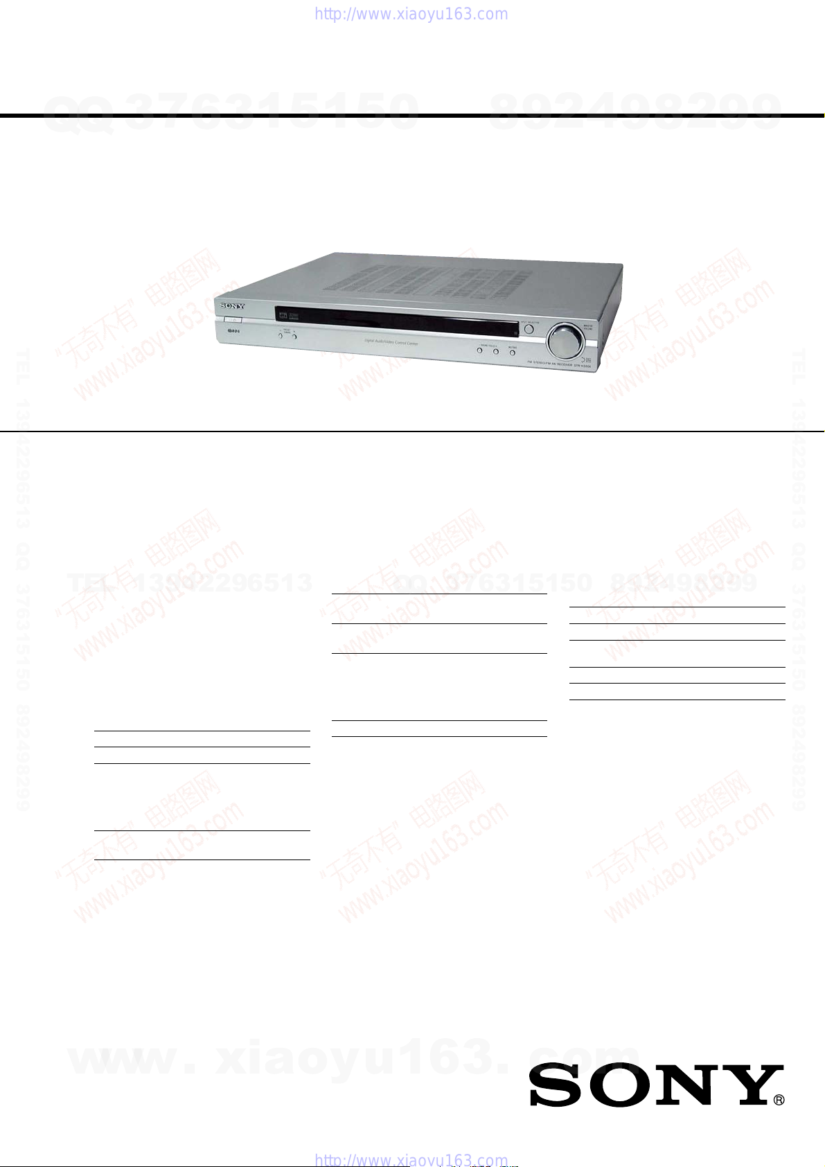
• STR-KS500 is the amplifier and tuner section in HT-SS500.
This receiver incorporates Dolby* Digital and Pro Logic Surround and the
DTS** Digital Surround System.
* Manufactured under license from Dolby Laboratories. “Dolby”, “Pro
Logic” and the double-D symbol are trademarks of Dolby Laboratories.
** “DTS” and “DTS Digital Surround” are registered trademarks of Digital
Theater Systems, Inc.
8
9
2
4
9
2
8
9
AEP Model
UK Model
9
TEL 13942296513 QQ 376315150 892498299
Amplifier section
TEL
13942296513
Power Output
Stereo mode (rated) 30 W + 30 W
1)
Measured under the following conditions:
Area code Power requirements
CEL, CEK 230 V AC, 50 Hz
2)
Depending on the sound field settings and the
source, there may be no sound output.
Inputs (Analog)
SA-CD/CD, Sensitivity: 900 mV
VIDEO 1, 2 Impedance: 50 kohms
1)
(6 ohms at 1 kHz, 0.7%)
Music power output
FRONT2): 63.3 W/ch
CENTER2): 63.3 W
SUR2): 63.3 W/ch
SUBWOOFER2): 63.5 W
SPECIFICATIONS
Inputs (Digital)
DVD (Coaxial) Sensitivity: –
SA-CD/CD (Optical) Sensitivity: –
Reproduction frequency range:
Tone
Gain levels ±6 dB, 1 dB step
FM tuner section
Tuning range 87.5 - 108.0 MHz
Antenna FM wire antenna
Antenna terminals 75 ohms, unbalanced
Intermediate frequency
AM tuner section
Tuning range
Models of area code CEL, CEK
With 9-kHz tuning scale:
Antenna Loop antenna
Intermediate frequency
Q
Q
7
3
Impedance: 75 ohms
Impedance: –
28 – 20,000 Hz
10.7 MHz
531 – 1,602 kHz
450 kHz
6
3
1
5
General
8
0
5
1
Power requirements
Area code Power requirements
CEL, CEK 230 V AC, 50/60 Hz
Power consumption
Area code Power consumption
CEL, CEK 180 W
Power consumption (during standby mode)
Dimensions (w/h/d) (Approx.)
Mass (Approx.) 5.7 kgSpeaker
Design and specifications are subject to change
without notice.
4
2
9
0.2 W
430 × 64 × 352 mm
including projecting parts
and controls
9
8
2
9
9
w
w
9-887-302-02
2006H05-1
© 2006.08
w
.
xia
Sony Corporation
Home Audio Division
Published by Sony Techno Create Corporation
o
y
u
1
6
FM STEREO/FM-AM RECEIVER
3
.
c
o
m
STR-KS500
Notes on chip component replacement
• Never reuse a disconnected chip component.
Q
Q
• Notice that the minus side of a tantalum capacitor may be
damaged by heat.
UNLEADED SOLDER
Boards requiring use of unleaded solder are printed with the leadfree mark (LF) indicating the solder contains no lead.
(Caution: Some printed circuit boards may not come printed with
the lead free mark due to their particular size)
: LEAD FREE MARK
Unleaded solder has the following characteristics.
• Unleaded solder melts at a temperature about 40 °C higher
than ordinary solder.
TEL 13942296513 QQ 376315150 892498299
Ordinary soldering irons can be used but the iron tip has to be
applied to the solder joint for a slightly longer time.
Soldering irons using a temperature regulator should be set to
about 350 °C.
Caution: The printed pattern (copper foil) may peel away if
the heated tip is applied for too long, so be careful!
• Strong viscosity
Unleaded solder is more viscou-s (sticky, less prone to flow)
than ordinary solder so use caution not to let solder bridges
occur such as on IC pins, etc.
• Usable with ordinary solder
It is best to use only unleaded solder but unleaded solder may
also be added to ordinary solder.
TEL
3
7
6
3
1
13942296513
5
1
5
0
1. GENERAL ................................................................... 3
2. DISASSEMBLY
2-1. Disassembly Flow ........................................................... 5
2-2. Case (SL500) ................................................................... 5
2-3. Front Panel Assy.............................................................. 6
2-4. MAIN Board.................................................................... 6
3. TEST MODE.............................................................. 7
4. DIAGRAMS
4-1. Block Diagram – AUDIO DSP Section –........................ 8
4-2. Block Diagram – TUNER/AUDIO AMP Section –........ 9
4-3. Block Diagram
– DISPLAY/POWER SUPPLY Section – ....................... 10
4-4. Printed Wiring Board
– DIGITAL Board (Component Side) – .......................... 12
4-5. Printed Wiring Board
– DIGITAL Board (Conductor Side) –............................ 13
4-6. Schematic Diagram – DIGITAL Board (1/3) – ............... 14
4-7. Schematic Diagram – DIGITAL Board (2/3) – ............... 15
4-8. Schematic Diagram – DIGITAL Board (3/3) – ............... 16
4-9. Schematic Diagram – MAIN Section (1/3) – .................. 17
4-10. Schematic Diagram – MAIN Section (2/3) – .................. 18
4-11. Schematic Diagram – MAIN Section (3/3) – .................. 19
4-12. Printed Wiring Board – MAIN Board – .......................... 20
4-13. Printed Wiring Boards
– SPEAKER/STANDBY Boards – ................................. 21
4-14. Printed Wiring Boards – PANEL Section –..................... 22
4-15. Schematic Diagram – PANEL Section –......................... 23
Q
Q
5. EXPLODED VIEWS
5-1. Front Panel Section ......................................................... 32
5-2. Chassis Section................................................................ 33
3
7
TABLE OF CONTENTS
4
2
9
8
8
0
5
1
5
1
3
6
9
9
8
2
4
2
9
8
9
2
9
9
TEL 13942296513 QQ 376315150 892498299
9
SAFETY-RELATED COMPONENT WARNING!!
COMPONENTS IDENTIFIED BY MARK 0 OR DOTTED LINE
WITH MARK 0 ON THE SCHEMATIC DIAGRAMS AND IN
THE PARTS LIST ARE CRITICAL TO SAFE OPERATION.
w
w
REPLACE THESE COMPONENTS WITH SONY P AR TS WHOSE
PART NUMBERS APPEAR AS SHOWN IN THIS MANU AL OR
IN SUPPLEMENTS PUBLISHED BY SONY.
w
.
xia
o
y
6. ELECTRICAL PARTS LIST................................ 34
u
1
6
3
.
c
o
m
2
1 2 3 4 5
21 3 4 5 6
SECTION 1
GENERAL
STR-KS500
This section is extracted from
instruction manual.
Q
Q
7
3
Getting Started
6
3
1
5
1
5
0
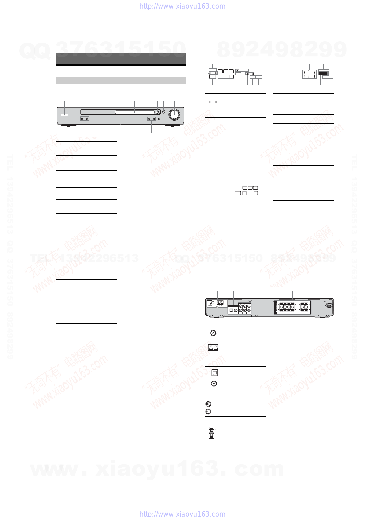
Description and location of parts
Receiver
Front panel
?/1
Name Function
TEL 13942296513 QQ 376315150 892498299
A ?/1 Press to turn the receiver
B Display The current status of the
C Remote sensor Receives signals from
D INPUT
SELECTOR
E MASTER
VOLU ME
F MUTING Press to mute the sound.
G SOUND FIELD
+/–
H PRESET TUNING
+/–
PRESET
TUNING
on or off.
selected component or a
list of selectable item s
appears here.
remote commander.
Press to select the input
source to playback.
Turn to adjust the volume
level of all speakers at the
field.
Press to select a sound
field.
Press to select a preset
station.
INPUT SELECTOR
SOUND FIELD MUTING
78 6
MASTER
VOLUME
About the indicators on the display
SLEEP
LFE
SW
Name Function
A Lights up when the disc being
LFE
B
SLEEP
C
Playback
channel
indicators
L
R
C
SL
SR
S
D ;
9
8
L
CR
S
SL SR
played back contains an LFE
(Low Frequency Effect) channel
and the LFE channel signal is
actually being reproduced.
Lights up when the sleep timer is
activated.
The letters (L, C, R, etc.) indicate
the channels being played back.
The boxes around the letters vary
to show how the receiver
downmixes the source sound.
Front Left
Front Right
Center (monaural)
Surround Left
Surround Right
Surround (monaural or the
surround components obtained
by Pro Logic processing)
Example:
Recording format (Front/
Surround): 3/2.1
Sound Field: A.F.D. AUTO
DIGITAL
Lights up when Dolby Digital
signals are input.
Note
When playing a Dolby Digital
format disc, be sure that you
have made digital co nnections
and the audio input mode for
SA-CD/CD input is not set to
“CD ANLG”.
DTS
SW
2
DIGITAL
L
SL SR
PL
COAX
OPT
CR
4
9
Name Function
E
F
G
H
I
J
Preset
station
indicators
D.RANGE
Tuner
indicators
MEMORY
COAX
OPT
8
2
9
D.RANGE
RDS
MEMORY
ST MONO
789q;qaqsqd
Lights up when using the
receiver to tune in radio stations
you have preset. For details on
presetting radio stations.
Lights up when dynamic range
compression is activated.
Lights up when using the
receiver to tune in radio stations,
etc.
Note
“RDS” lights up for models of
area code CEL, CEK only.
Lights up when a memory
function, such as Preset Memory,
etc., is activated.
Lights up when the DVD input is
selected.
Lights up when
–the audio input mode for SA-
CD/CD input is set to “CD
AUTO” and the source signal
is a digital signal being input
through the SA-CD/CD OPT
IN jack.
–the audio input mode for
SA-CD/CD input is set to
“CD OPT”.
9
TEL 13942296513 QQ 376315150 892498299
TEL
13942296513
Name Function
K ;PL(II) Lights up when the receiver
L DTS Lights up when DTS signals are
M SW Lights up when the audio signal
applies Pro Logic processing to 2
channel signals in order to output
the center and surround channel
signals. “; PLII” lights up
when the Pro Logic II Movie/
Music decoder is activated.
Note
Dolby Pro Logic and Dolby Pro
Logic II decoding do not
function for DTS format signals.
input.
Note
When playing a DTS format
disc, be sure that you have made
digital connections and the audio
input mode for SA-CD/CD input
is not set to “CD ANLG”.
is output from the
SUBWOOFER jack.
Q
Q
3
6
7
3
Rear panel
1
ANTENNA
AM
U
A ANTENNA section
B DIGITAL INPUT section
C AUDIO INPUT section
D SPEAKER section
White (L)
Red (R)
FM
ANTENNA
AM
ANTENNA
OPTICAL
IN jack
COAXIAL
IN jack
AUDIO I N
jack
9
8
0
5
1
5
1
2 3 4
SA-CD/CD
VIDEO 2
VIDEO 1
LRL
DIGITAL
OPT IN
COAX IN
AUDIO IN
SA-CD/CD
DVD
Connects to a DVD
player, etc. The CO AX
IN jack provides a
better quality of loud
sound.
Connects to a satellite
tuner, CD player, etc.
Connects to speakers
and sub woofer.
R
AUDIO IN
AUDIO IN
Connects to the
FM wire antenna
supplied with this
receiver.
Connects to the
AM loop antenna
supplied with this
receiver.
SPEAKERS
4
2
LRLR
LRLR
FRONT CENTER
SURROUND
9
WOOFER
SUB
8
2
9
9
w
w
w
.
xia
o
y
u
1
6
3
.
c
o
m
3
STR-KS500
7
Remote commander
Q
Q
You can operate the receiver with the supplied
remote. You can also use the remote to control
the Sony audio/video components that the
remote is assigned to operate.
wg
wf
wd
ws
wa
w;
ql
qk
TEL 13942296513 QQ 376315150 892498299
qj
qh
3
TV/VIDEO
TEST
AV
?/1
SLEEP
TONE
SYSTEM STANDBY
VIDEO 1 VIDEO 2 DVD SA-CD/CD
TUNER
MAIN MENU
2CH A.F.D.
MOVIE MUSIC
DUAL MONO
12 3
FM MODE
46
5
D.TUNING
9
78
SUBTITLE
MEMORY SHIFT
>10
0/10
ENTER
-
D.SKIPCLEAR ANGLE
AV
TOP MENU/
MENU
GUIDE MUTING
F
MASTER VOL
ENTER
Gg
f
RETURN/EXIT
DISPLAY
TV CH –
c STEP C
REPLAY ADVANCE
PRESET –
TUNING –TVTUNING +
<
.
HmM
Xx
<
PRESET +
TV
?/1
MPX
AUDIO
ANT
JUMP
TV VOL
TV CH +
>
?/1
AV ?/1
1
(on/standby) switch
TV ?/1, ?/1
2
(on/standby) switch
3
4
5
6
7
8
9
q;
qa
qs
qd
qf
qg
Name Function
6
1
3
A AV ?/1 Press to turn on or off the Sony
B TV ?/1 Press TV ?/1 and TV (P) at
?/1 Press to turn the receiver on or
C Input buttons Press one of the buttons to
D MAIN MENU Press to display the menu of
E MOVIE,
MUSIC
F DUAL MONO Press to select the language
5
1
audio/video components that
the remote is assigned to
operate.
If you press ?/1 (B) at the
same time, it will turn off the
receiver and other components
(SYSTEM STANDBY).
Note
The function of the AV ?/1
switch changes automatically
each time you press the input
buttons (C).
the same time to turn the TV
on or off.
off.
To tu rn of f al l components,
press ?/1 and AV ?/1 (A) at
the same time (SYSTEM
STANDBY).
select the component you want
to use. When you press any of
the input buttons, the rece iver
turns on. The buttons are
factory assigned to control
Sony components as follows.
You can change the button
assignments following the
steps in “Changing button
assignments”.
Button Assigned Sony
component
VIDEO 1 VCR (VTR mode 3)
VIDEO 2 VCR (VTR mode 2)
DVD DVD player
SA-CD/CD Super Audio CD/CD
player
TUNER Built-in tuner
the receiver. Then, use the
control buttons to perform
menu operations.
Press to select sound fields for
movie or music.
you want during digital
broadcast.
5
Name Function
0
G
FM MODE
MPX
AUDIO
H
D.TUNING
ANT
SUBTITLE
I
ENTER
MEMORY
D.SKIP
J
JUMP
ANGLE
K
AV M E N U
MUTING
L
TV VOL
M
a)
/–
+
MASTER
a)
/–
VOL +
Press to select FM monaural or
stereo reception.
Press to select the main or sub
language of the VCR.
Press to change the sound to
Multiplex, Biligual or Multi
channel TV sound of the DVD
player or satellite tuner.
Press to enter direct tuning
mode.
Press to select the output signal
from the antenna terminal (TV
signal or VCR program) of the
VCR or satellite tuner.
Press to change the subtitles of
the DVD player.
Press to enter the value after
selecting a channel, disc or
track using the numeric
buttons.
Press to store a station.
Press to skip disc of the CD
player or DVD player (multidisc changer only).
Press to toggle between the
previous and the current
channels of the satellite tuner.
Press to select the viewing
angle or to change the angles
of the DVD player.
Press to display the menus of
the VCR, DVD player, or
satellite tuner on the TV
screen. Then, use the control
buttons to perform menu
operations.
Press to mute the sound.
Press TV VOL +/– and TV
(P) at the same time to adjust
the TV volume level.
Press to adjust the volume
level of all speakers at the
same time.
8
9
2
Name Function
4
N
DISPLAY
O .
/
> Press to skip tracks of the CD
STEP C,
c
<
REPLAY /
ADVANCE
/
M Press to
m
a)
H
X Press to pause playback or
x Press to stop playback of the
TV CH +/–
PRESET +/–
TUNING +/–
8
9
Press to
–select information disp lay ed
on the receiver’s display (for
TUNER input only).
–select information displayed
on the TV screen of the
VCR, satellite tuner, CD
player, DVD player, or MD
deck.
player, DVD player, MD deck,
or tape deck.
Press to replay the previous
scene or fast forward the
<
current scene of the VCR or
DVD player.
–search tracks in the forward/
backward direction of the
DVD player.
–fast forward/rewind of the
VCR, CD player, MD deck,
or tape deck.
Press to start playback of the
VCR, CD player, DVD player,
MD deck, or tape deck.
recording of the VCR, CD
player, DVD player, MD deck,
or tape deck. (Also starts
recording with components in
recording standby.)
VCR, CD player, DVD player,
MD deck, or tape deck.
Press TV CH +/– and TV ( P)
at the same time to select
preset TV channels.
Press to select
–preset stations.
–preset channels of the VCR
or satellite tuner.
Press to scan a station.
2
b)
9
9
TEL 13942296513 QQ 376315150 892498299
TEL
Name Function
P TV To activate the buttons with
Q RETURN/
EXIT O
R Control
buttons
S TOP MENU/
GUIDE
T -/-- Press -/-- and TV (P) at the
>10 Press to select track numbers
CLEAR Press to
U Numeric
buttons
(number 5
13942296513
orange printing, press TV and
the button with orange
printing simultaneously .
Press to
–return to the previous menu.
–exit the menu while the
menu or on-screen guide of
the DVD player, or satellite
tuner is displayed on the TV
screen.
After pressing MAIN MENU
(D), AV MENU (K), or
TOP MENU/GUIDE (S),
press the control button V, v,
B or b to select the settings.
When you press A V MENU or
TOP MENU/GUIDE, press
ENTER to enter the selection.
Press to display the
–DVD title of the DVD
player.
–guide menu of the satellite
tuner.
same time to select the
channel entry mode, ei ther
one or two digits of the TV.
over 10 of the VCR, CD
player, or MD deck.
–clear a mistake when you
press the incorrect numeri c
button.
–return to continuous
playback, etc. of the satellite
tuner or DVD player.
Press to
–preset/tune to preset
a)
stations.
)
–select track numbers of the
CD player, DVD player or
MD deck. Press 0/10 to
select track number 10.
–select channel numbers of
the VCR or satellite tuner.
Press the numeric but tons and
TV (P) at the same time to
select the TV channels.
Name Function
V 2CH Press to select 2CH STEREO
W A.F.D. Press to select A.F.D. mode.
X TEST TONE Press to activate the T est Tone
Y TV/VIDEO Press TV/VIDEO and TV
SLEEP Press to activate the Sleep
a)
The number 5, MASTER VOL +, TV V OL +, and
H buttons have tactile dots. Use t he tactile dots as
references when operating the receiver.
b)
Models of area code CEL, CE K o nly.
Notes
•Some functions explained in this section may not
work depending on the m o del.
•The above expl anation is intended to serve as an
example on ly. Therefore, depending on the
component, the above operation may not be
possible or may operate differently than described.
•The SHIFT button on the remote is not available
for receiver operation.
mode.
function.
(P) at the same time to select
the input signal (TV input or
video input).
Timer function a nd the
duration which the receiver
turns off automatically.
Q
Q
3
7
6
3
1
5
1
5
0
8
9
2
4
9
8
2
9
9
4
w
w
w
.
xia
o
y
u
1
6
3
.
c
o
m
Q
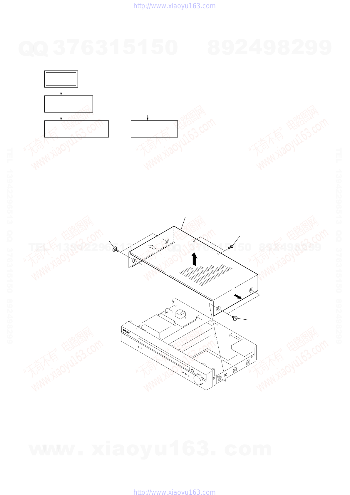
• This set can be disassembled in the order shown below.
7
Q
3
2-1. DISASSEMBLY FLOW
SET
2-2. CASE (SL500)
(Page 5)
6
3
1
5
1
SECTION 2
DISASSEMBLY
5
0
8
9
2
4
9
STR-KS500
2
8
9
9
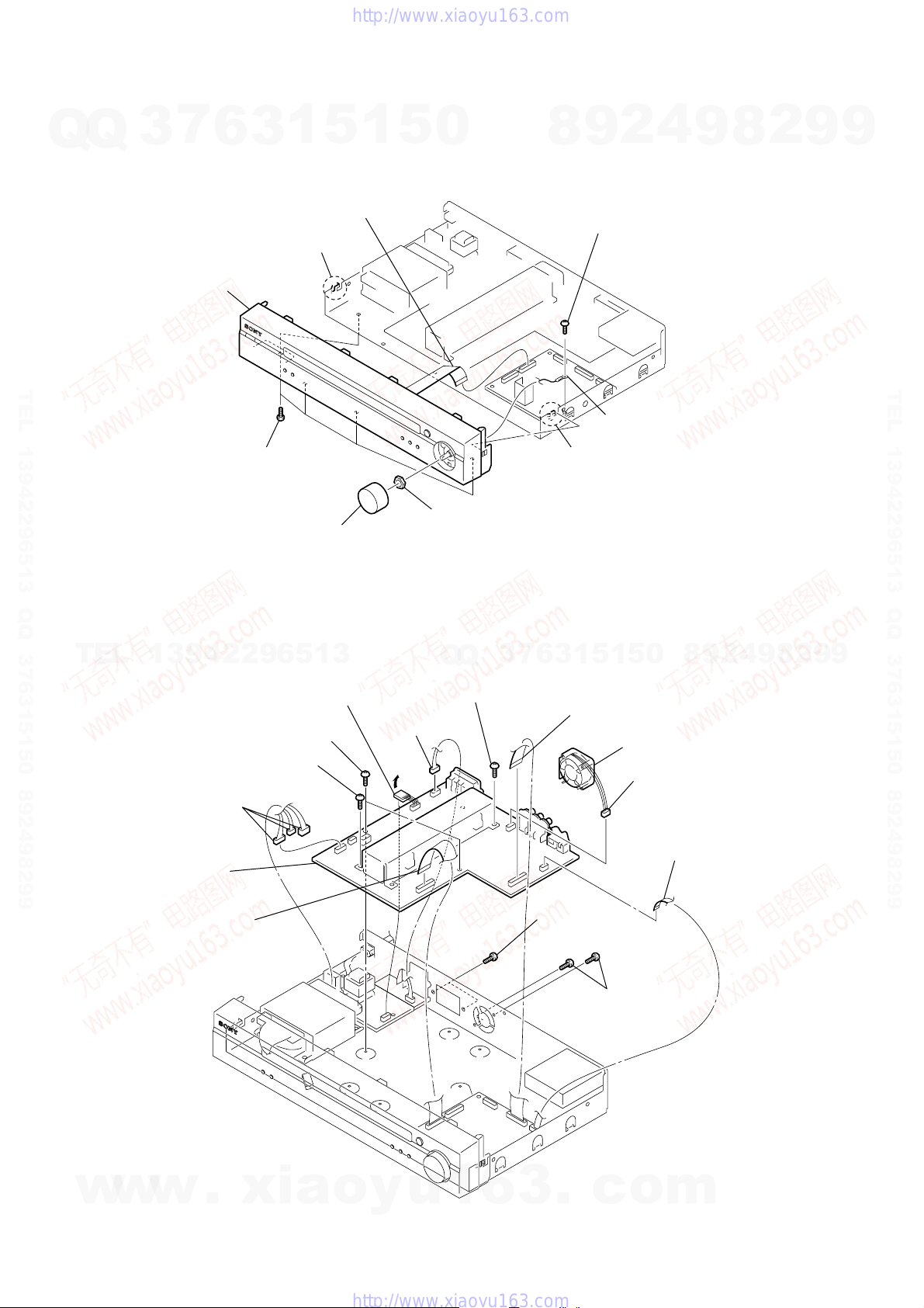
2-3. FRONT PANEL ASSY
(Page 6)
TEL 13942296513 QQ 376315150 892498299
Note: Follow the disassembly procedure in the numerical order given.
2-2. CASE (SL500)
2
two screws
(case 3 TP2)
TEL
13942296513
2-4. MAIN BOARD
(Page 6)
5
3
Q
case (SL500)
7
3
Q
4
6
3
1
5
1
1
two screws
(BVTP3
0
5
3
8
×
8)
9
2
4
9
8
2
9
TEL 13942296513 QQ 376315150 892498299
9
w
w
w
.
xia
o
y
u
1
6
3
.
c
o
2
two screws
(case 3 TP2)
m
5
STR-KS500
s
2-3. FRONT PANEL ASSY
7
Q
Q
3
8
front panel assy
6
3
1
5
1
1
wire (flat type) (17 core)
(CNS193)
5
claw
5
0
8
2
9
screw
(BVTP3
2
×
6)
4
9
8
2
9
9
TEL 13942296513 QQ 376315150 892498299
4
2-4. MAIN BOARD
TEL
2
13942296513
three connectors
(CNP801, CNP802, CNP804)
qf
MAIN board
four screws
(BVTP3
6
volume knob (SL500)
qa
screw
(BVTP3
3
qs
two screws
(BVTP3
×
6)
connector
(CNP903)
×
6)
×
10)
4
connector
(CN700)
7
Q
nut
Q
qd
3
screw
(BVTP3
×
7
10)
3
5
claw
1
5
1
3
6
5
wire (flat type) (21 core)
(CNS403)
harnes
2
9
8
0
5
9
D.C. fan (M1)
8
connector
(CNP861)
6
wire (flat type) (7 core)
(CNS301)
4
9
8
2
9
TEL 13942296513 QQ 376315150 892498299
9
6
1
w
w
wire (flat type) (21 core)
(CNS822)
w
.
xia
o
y
u
1
6
3
0
two screws
(BVTP3
7
two screws
(BVTP3
.
c
×
8)
×
8)
o
m
SECTION 3
TEST MODE
STR-KS500
SOUND FIELD CLEAR MODE
The preset sound field is cleared when this mode is activated. Use
Q
this mode before returning the product to clients upon completion
of repair.
Procedure:
RDS AUTOBETICAL MODE
Procedure:
TEL 13942296513 QQ 376315150 892498299
FACTORY PRESET MODE
All preset contents are reset to the default setting.
Procedure:
FL CHECK MODE
All fluorescent segments are tested. When this test is activated, all
segments turn on at the same time, then each segment turns on one
after another.
Procedure:
Q
1. While pressing the [SOUND FIELD +] button, press the I/1 button
to turn on the main power .
2. The message “S.F. CLR.” appears and initialization is
performed.
1. While pressing the [INPUT SELECTOR] button, press the I/1
button to turn on the main power.
2. The message “ A UTO-BETICAL SELECT” appears and scans
and stores all the FM and FM RDS stations in the broadcast
area.
3. When done, the message “FINISH” appears.
1. While pressing the [SOUND FIELD --] and [PRESET TUNING +]
buttons, press the I/1 button to turn on the main power.
2. The message “FACTORY” appears and the present contents
are reset to the default values.
T
E
1. While pressing the [MUTING] and [PRESET TUNING --] buttons,
press the
2. All segments turn on.
3. Press the [INPUT SELECTOR] button.
4. Half of segments turn on.
5. Press the [INPUT SELECTOR] button once again.
6. Others half of segments turn on.
7. Press the [INPUT SELECTOR] button once again.
8. All segments turn off.
L
I/1 button to turn on the main power.
3
1
3
7
9
4
6
2
2
COMMAND MODE CHANGE MODE
The command mode of the remote commander can be changed.
3
9
1
Procedure:
1. While pressing the [SOUND FIELD +] and [INPUT SELECTOR]
buttons, press the I/1 button to turn on the main power.
2. Either the message “C.MODE.AV 1” or “C.MODE.AV 2”
appears for a moment and select the desired mode.
SWAP ALL MODE
When this mode is used, output the audio signal of front L/R channel
to all channel.
Procedure:
1. While pressing the [PRESET TUNING +] and [MUTING] buttons,
press the I/1 button to turn on the main power.
2. The message “SWP. ALL” appears.
PROTECTOR AUTO OFF MODE
When this mode is used, a protector on state is maintainable.
Procedure:
1. While pressing the [MUTING] and [SOUND FIELD --] buttons,
press the I/1 button to turn on the main power.
2. The message “PLOT. EVER” appears.
ALL CLEAR MODE
All preset contents are cleared when this mode is activated. Use
this mode before returning the product to clients upon completion
of repair.
Procedure:
1. While pressing the [INPUT SELECTOR] and [PRESET TUNING +]
buttons, press the I/1 button to turn on the main power .
2. The message “CLEARED” appears and the memories are reset
to the default values.
6
5
1
5
3
1
5
0
Q
Q
3
7
6
8
3
1
9
5
1
2
5
0
4
8
9
9
2
8
4
9
2
8
2
9
9
9
TEL 13942296513 QQ 376315150 892498299
9
VERSION MODE
When this mode is used, the model, the destination and the software
version number are displayed.
Procedure:
KEY CHECK MODE
This mode is used to check the key.
Procedure:
STR-KS500
1. While pressing the [SOUND FIELD +] and [PRESET TUNING --]
buttons, press the I/1 button to turn on the main power.
2. The model, the destination and the software version number
appear.
1. While pressing the [MUTING] and [INPUT SELECTOR] buttons,
press the I/1 button to turn on the main power.
2. The message “REST 06” appears.
3. Every pressing of any button other than the I/1 button counts
down the buttons. The b uttons which are already counted once
are not counted again.
4. When all buttons are pressed, the message “REST 00” appears.
w
w
w
.
x
i
a
o
y
u
1
6
77
3
.
c
o
m
STR-KS500
Q
Q
3
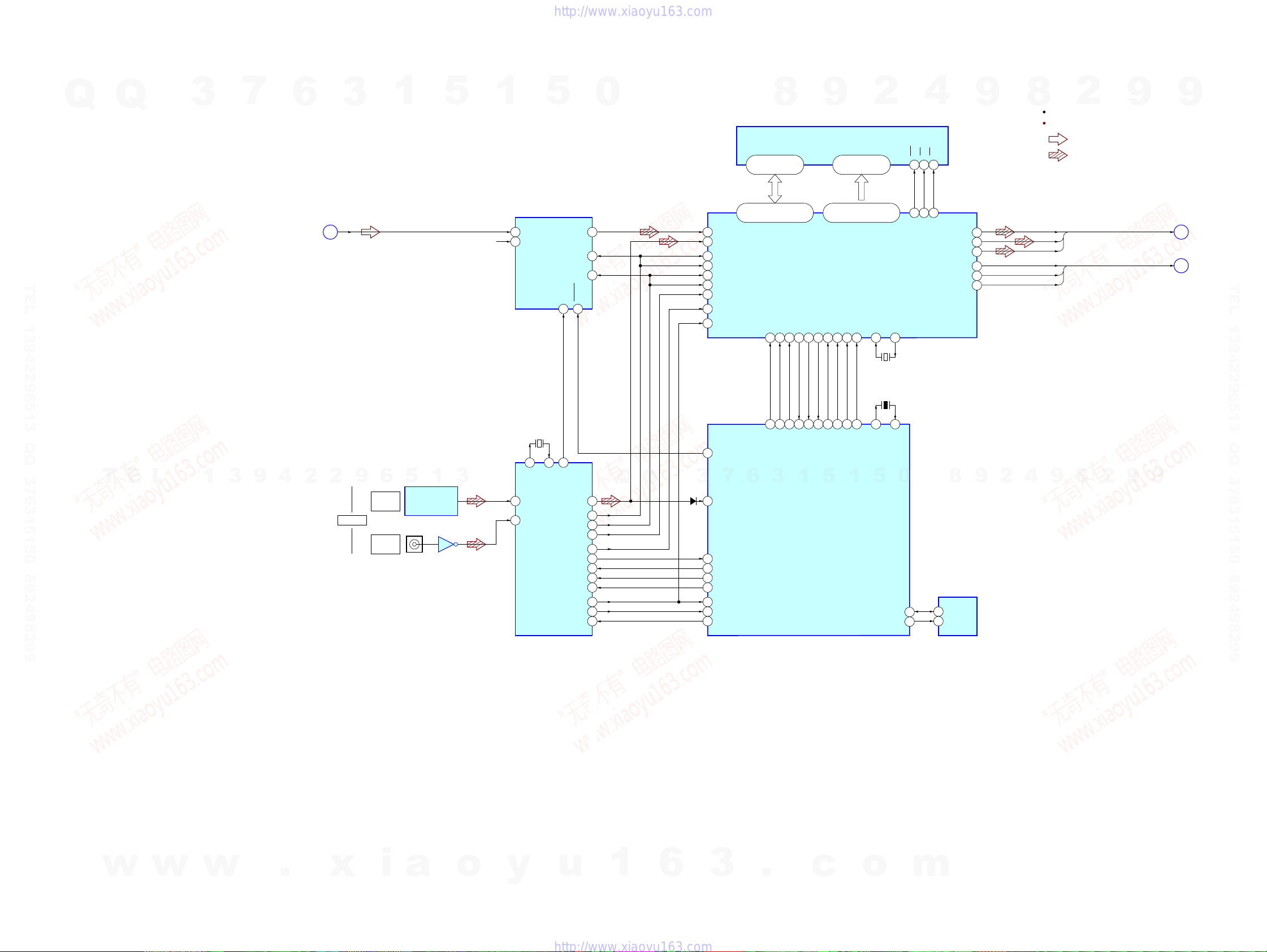
SECTION 4
DIAGRAMS
7
6
4-1. BLOCK DIAGRAM – AUDIO DSP Section –
3
1
5
1
5
0
8
D0 – D15 A0 – A15
7 – 10, 13 – 16,
29 – 32, 35 – 38
9
S-RAM
IC1502
5 – 1, 44 – 42,
27 – 24, 21 – 18
2
17
4
WEWE0
CSCE0
6
9
OEOE0
41
8
2
R-ch is omitted due to same as L-ch.
SIGNAL PATH
: AUDIO (ANALOG)
: AUDIO (DIGITAL)
9
9
L-CH
A
(Page 9)
TEL 13942296513 QQ 376315150 892498299
T
E
L
1
3
9
4
2
2
DIGITAL
9
6
SA-CD/CD
OPT IN
DVD
COAX IN
5
1
DIGITAL OPTICAL
RECEIVER
IC301
J301
IC303
3
R-CH
A/D CONVERTER
IC1602
1 12LIN DOUT
2RIN
SCKI
15
X1301
12.288MHz
20
22
21
XIN
XOUT
XMCK
4DIN1
5DIN2
PDWN
7
108, 107, 105 – 102,
99, 98, 80 – 77, 75 – 72
18 SDI1
30 SDI2
11BCK
10LRCK
Q
Q
16DATA0
14BCK
15LRCK
13CKOUT
24AUDIO
35DO
36DI
38CLK
37CE
34ERROR
17XSTATE
48XMODE
17 BCKI1
29 BCKI2
15 LRCKI1
28 LRCKI2
22 KFSIO
69 GP8
59 EXLOCK
3
D1301
98 DO
97 DI
95 CLK
96 CE
99 ERROR
100 XSTATE
93 XMODE
9 PCM1803_RST
7
1 DATAO
D0 – D15
33
19
6
HDINHDIN
HCLKHCLK
HCSHCS
34
36
20
4
3
SYSTEM CONTROLLER
IC1601 (1/3)
AUDIO DIGITAL
SIGNAL PROCESSOR
HDOUTHDOUT
HACNHACN
GP9GP9
35
32
68
37
18
5
2
8
5
1
112, 110, 109, 97 – 92,
82 – 85, 66 – 64
A0 – A15
IC1501
GP12GP12
56
3
BSTBST
113
7
PMPM
1
2
6
XRSTXRST
MCLK1
9
X1502
13.9MHz
X1101
24MHz
83
X1
5
12
82
MCLK2
X0
0
29SDA
33SCL
45
44
43
SDO1 SDO1, SDO2, SDO3
SDO2
SDO3
4
BCKO
LRCKO
SCKO
9
8
BCKO, LRCKO, SCKO
9
2
(Page 9)
(Page 9)
9
B
C
TEL 13942296513 QQ 376315150 892498299
8
EEPROM
IC1131
5 SDA
6 SCL
23SDO1
24SDO2
25SDO3
20BCKO
19LRCKO
14SCKOUT
9
2
STR-KS500
w
w
w
.
x
i
a
o
DIGITAL AUDIO INTERFACE RECEIVER
y
IC1301
u
1
88
6
3
.
c
o
m
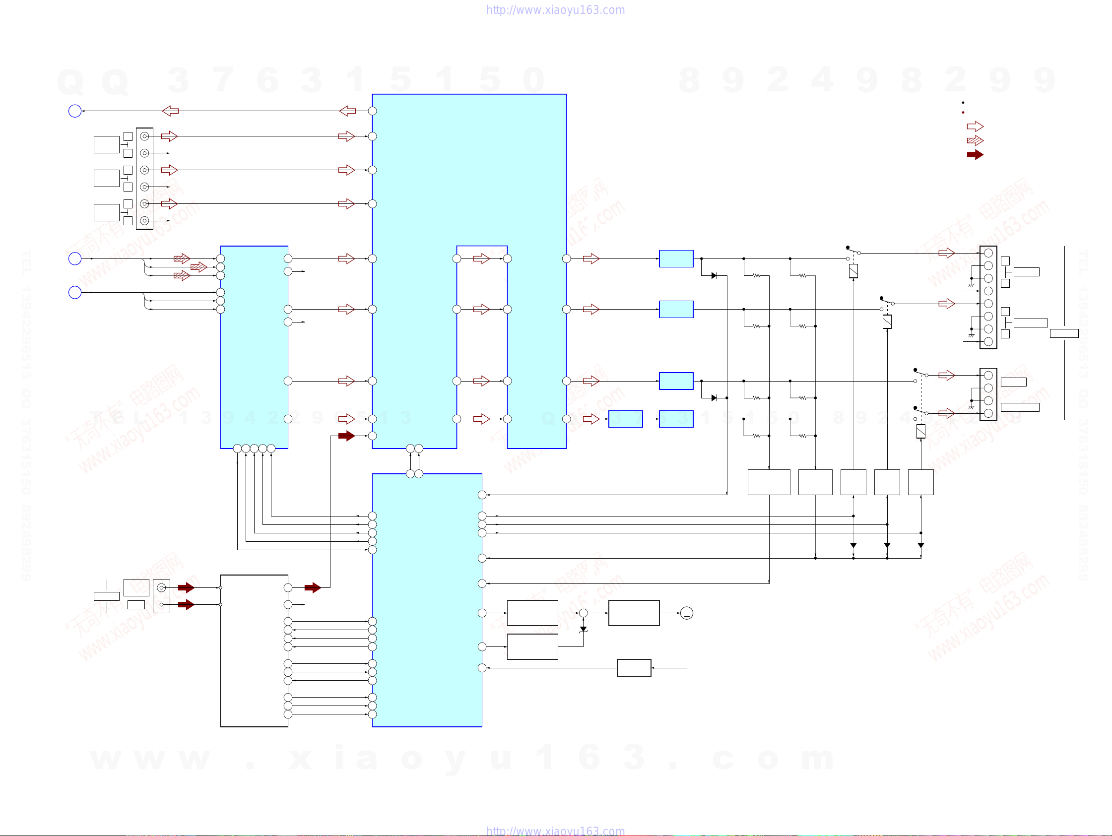
4-2. BLOCK DIAGRAM – TUNER/AUDIO AMP Section –
Q
A
(Page 8)
L-CH
Q
SA-CD/CD
AUDIO IN
VIDEO 1
AUDIO IN
3
J1710
L
R
L
R
R-CH
R-CH
7
6
3
1
13 ADIFL
2INL5
4INL4
5
1
AUDIO SELECTOR,
ELECTRICAL VOLUME
IC401
5
0
8
9
2
4
9
8
STR-KS500
2
9
R-ch is omitted due to same as L-ch.
SIGNAL PATH
: AUDIO (ANALOG)
: AUDIO (DIGITAL)
: TUNER
9
E
L
R
L
FM 75Ω
COAXIAL
AM
SDO1SDO1, SDO2, SDO3
SDO2
SDO3
BCKOBCKO, LRCKO, SCKO
LRCKO
SCKO
R-CH
1
3
D/A CONVERTER
47 DATA3
45 DATA1
46 DATA2
40 BCK
41 LRCK
38 SCKI
9
FM
AM
IC1452
4
2
MDI34MDO33MC35ML36RST
TN1
TUNER
9VOUT6
R-CH
14VOUT1
13VOUT2
R-CH
12VOUT3
11VOUT4
2
9
6
37
8L CH
10R CH
R-CH
2
DO
3DATA
1CLOCK
4CE
VIDEO 2
AUDIO IN
TEL 13942296513 QQ 376315150 892498299
B
(Page 8)
C
(Page 8)
T
ANTENNA
6INL3
16 LIN 51 LVIN10VOUT5 52LIGO
19 SLIN
20 CIN
21 SWIN
5
1
3
8INL2
10 PCM1602_RST
12 PCM1602_ML
13 PCM1602_MC
14
PCM1602_MDI
15
PCM1602_MDO
69 DO
17 TUNER_DATA
16 TUNER_CLK
68 SLATCH
66 TUNED6TUNED
65 STEREO7STEREO
64 MUTE11MUTING
DATA
24
21
VOL_DATA
SYSTEM CONTROLLER
IC1601 (2/3)
CLOCK
26
22
VOL_CLK
TM500
7
POWER AMP
IC701
POWER AMP
IC651
POWER AMP
IC501
POWER AMP
6
IC601
3
D529
D729
0
5
1
5
1
FAN MOTOR
LEVEL DETECT
Q550, 551
M1
M
(FAN)
PROTECTOR
AC POWER
Q730 – 732
RY701
8
RELAY
DRIVE
Q720
9
RY601
D721,
D1110
2
RELAY
DRIVE
Q620
4
RY501
D621,
D1108
RELAY
DRIVE
Q520
-2
-1
9
D521,
D1107
R-CH
R-CH
8
49LOUT
38 SLVIN37SLIGO
35 CVIN36CIGO
30 SWVIN29SWIGO
46FAN-HI-DETECT
70FRONT RELAY
72REAR RELAY
71CENTER RELAY
67PROTECTOR
76LEVEL_DETECT
73F_CTRL1
74F_CTRL2
75FAN_CLK
FAN MOTOR
CONTROL SWITCH
Q867, 868
FAN MOTOR
CONTROL SWITCH
Q862, 863
Q
40SLOUT
33COUT
32SWOUT
Q
LINE AMP
3
IC402
FAN MOTOR
D820
ON/OFF SWITCH
Q861
LEVEL SHIFT
Q866
+
2
+
–
–
+
+
–
–
+
TM501
+
–
–
+
9
L
FRONT
R
L
SURROUND
R
CENTER
SUB WOOFER
9
TEL 13942296513 QQ 376315150 892498299
SPEAKERS
STR-KS500
w
w
w
RDS DATA
FM SIG OUT
.
RDS INT
x
i
5315
5214
4313
a
RDS DATA
RDS CLK
RDS SIGNAL
o
y
u
1
6
99
3
.
c
o
m
STR-KS500
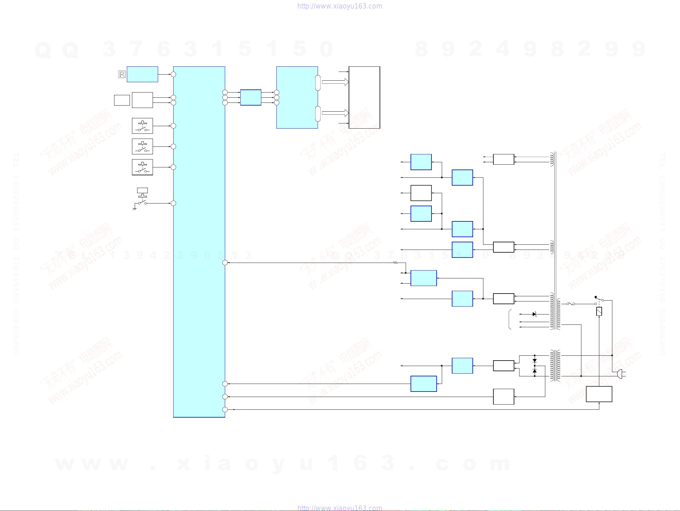
4-3. BLOCK DIAGRAM – DISPLAY/POWER SUPPLY Section –
MASTER
VOLUME
S120, 121
S119, 122
3
7
REMOTE CONTROL
RECEIVER
IC102
ROTARY
ENCODER
RV101
S123
I
/ 1
9
4
6
2
3
54 SIRCS
60 VOL (A)
59 VOL (B)
38 A/D0
39 A/D1S117, 118
40 A/D2
56 POWER KEY
SYSTEM CONTROLLER
IC1601 (3/3)
2
9
Q
TEL 13942296513 QQ 376315150 892498299
T
Q
E
L
3
1
1
6
5
5
61DIN
62CLK
63FL_STB
55FUSE DETECT
1
LEVEL SHIFT
IC1651
3
1
FLUORESCENT INDICATOR TUBE DRIVER
7 DIN
8 CLK
9 STB
5
IC152
0
42 – 31
GRID1 – GRID12
14 – 29
SEG1 – SEG16
F1
F2
Q
Q
FL1001
FLUORESCENT
INDICATOR
TUBE
3
TUNER+3.3V
TUNER+9V
+3.3V
A+5V, D+5V
+7V
–7V
7
6
8
+3.3V
REGULATOR
IC1071
+3.3V
REGULATOR
Q401
+5V
REGULATOR
IC1001
3
1
9
5
+9V
REGULATOR
IC1902
+7V
REGULATOR
IC403
–7V
REGULATOR
IC404
1
2
5
9
2
8
2
9
9
9
TEL 13942296513 QQ 376315150 892498299
9
4
B+
B–
0
RECT
D809
RECT
D801 – 804
8
9
9
MAIN POWER
TRANSFORMER
2
8
T901
4
D+3.3V
D+1.85V
+5V
STBY +3.3V
77RSTX
48STOP
78POWER RELAY
+1.85V/+3.3V
REGULATOR
IC1901
RESET SIGNAL
GENERATOR
IC1111
+5V
REGULATOR
IC1031
FLUORESCENT INDICATOR TUBE
+3.3V
REGULATOR
IC1904
(FL101)
RECT
D805 – 808
RECT
D952 – 955
AC POWER
DETECT
Q901
–30V
F1
F2
D956
D957
D813
T902
SUB POWER
TRANSFORMER
F901
RY901
POWER ON/OFF
RELAY DRIVE
Q951
(AC IN)
STR-KS500
w
w
w
.
x
i
a
o
y
u
1
1010
6
3
.
c
o
m

STR-KS500
• Note for Printed Wiring Boards and Schematic Diagrams
Q
Note on Printed Wiring Board:
• X : parts extracted from the component side.
• Y : parts extracted from the conductor side.
•
• : Pattern from the side which enables seeing.
(The other layers' patterns are not indicated.)
• Indication of transistor
TEL 13942296513 QQ 376315150 892498299
Q
f
: internal component.
Caution:
Pattern face side: Parts on the pattern face side seen from
(Conductor Side) the pattern face are indicated.
Parts face side: Parts on the parts face side seen from
(Component Side) the parts face are indicated.
C
Q
B
E
These are omitted.
3
7
6
3
1
Note on Schematic Diagram:
• All capacitors are in µF unless otherwise noted. (p: pF)
50 WV or less are not indicated except for electrolytics
and tantalums.
• All resistors are in Ω and 1/
specified.
• f : internal component.
• 2 : nonflammable resistor.
• 5 : fusible resistor.
• C : panel designation.
Note: The components identified by mark 0 or dotted line
• A : B+ Line.
• B : B– Line.
• Voltages and waveforms are dc with respect to ground
under no-signal (detuned) conditions.
no mark : TUNER
• Voltages are taken with a VOM (Input impedance 10 MΩ).
Voltage variations may be noted due to normal production tolerances.
• Waveforms are taken with a oscilloscope.
Voltage variations may be noted due to normal production tolerances.
• Circled numbers refer to waveforms.
• Signal path.
F : AUDIO (ANALOG)
J : AUDIO (DIGITAL)
f : TUNER
5
with mark 0 are critical for safety.
Replace only with part number specified.
1
4
W or less unless otherwise
5
0
• Circuit Boards Location
8
POWER board
TUNING board
9
STANDBY board
2
DISPLAY board
4
9
SPEAKER board
DIGITAL board
8
MAIN board
2
9
TUNER
9
TEL 13942296513 QQ 376315150 892498299
T
E
L
1
3
9
4
2
2
9
6
5
1
3
Q
Q
3
7
6
3
1
5
1
5
0
8
9
2
4
9
8
2
9
9
STR-KS500
w
w
w
.
x
i
a
o
y
u
1
6
1111
3
.
c
o
m
STR-KS500
3
7
9
6
• Semiconductor
Location
Ref. No. Location
D1301 D-7
IC1111 G-3
IC1131 D-2
IC1301 D-7
IC1452 D-5
IC1501 F-6
IC1502 F-7
IC1601 E-3
IC1602 D-6
IC1651 E-2
4
2
2
3
9
Q
Q
3
TEL 13942296513 QQ 376315150 892498299
T
E
L
1
1
6
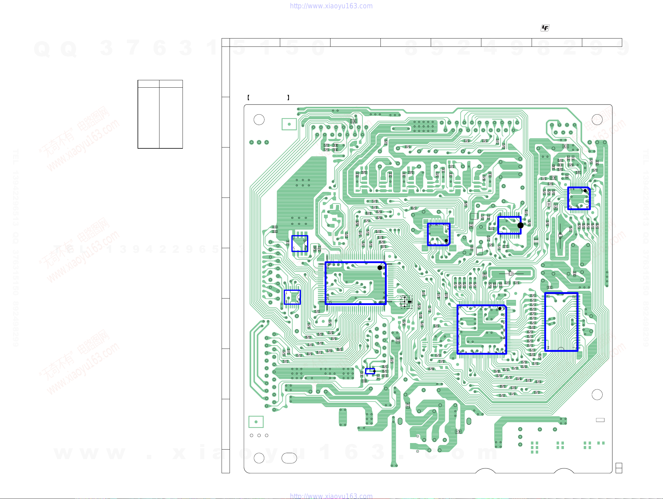
4-4. PRINTED WIRING BOARD – DIGITAL Board (Component Side) –
1 2 3 4 5 6 7 8
5
1
5
0
A
DIGITAL BOARD (COMPONENT SIDE)
C
R1168
1163
R
IC1601
R1119
1432
R1153
C1108
1128
R
FB1352
R1435
R1162
R1152
1151
R
3
1121
1156
R
R
IC1111
31
45
R1161
R1154
C1137
R1440
R1160
7
C1472
R1150
130
8051
R1149
R1144
R
R1143
81
R1127
R1189
C1107
1476
C
6
100
FB1101
R
5
B
C
D
E
F
G
1
3
C1122
C1123
IC1131
C1124
R1252
R1251
1157
R
31
1147
R
Q
C1253
C1252
Q
IC1651
50
R1070
1124
R1125
R1186
R1115
R1126
R
R1105
R1123
R1112
1129
R
R1122
R1113
1109
1110
R
R
R1107
R1053
1441
1106
FB1502
8
3
X1101
1041
R
R1436
1135
R
R1445
R1137
1134
R
R1460
1
25
36
R1511
9
1484
R
IC1452
5
1136
R
R1142
: Uses unleaded solder.• See page 11 for Circuit Boards Location.
1307
R1306
1301
FB1302
R1303
R1304
FB1301
1308
R
FB1305
1301
X
9
C1913
IC1502
1302
C
2
C1304
R1301
C1305
13
IC1301
24
R1310
8
C1063
C1301
R1302
2
9
9
TEL 13942296513 QQ 376315150 892498299
1361
R
1131
C
R1362
112
48
37
3625
1312
R
R1313
9
R1315
1316
R
9
1311
R
L1604
0
1503
R
R1486
FB1503
4
1464
R
1672
R
1608
R
L1605
1502
R
IC1501
R1671
R1607
R1535
R1536
C1462
1675
C
1523
R
R1542
R1527
1466
R
IC1602
8
R1606
1522
C
1426
R
R1515
1521
C
130
9061
R1547
C1659
X1502
120
91
R1537
9
110
2011
9
R1501
R1517
R1518
R1519
R1522
R1534
R1538
R1543
R1528
R1548
R1549
R1550
R1526
R1525
R1552
R1553
R1554
R1521
R1520
R1533
2
R1532
R1539
1609
R
1618
R
R1305
8
C1303
R1360
D
1309
R
1020
JR
4
1557
R
R1551
R1540
R1544
R
2
R1446
R1425
C1483
1422
C
R1470
1324
FB1452
12
1
C1454
4837
5
1
1509
R1508
R
R1555
R1529
R1541
1505
1506
R1504
R
R
31
60
STR-KS500
w
w
w
.
x
i
a
o
FB1501
y
u
1
6
3
.
c
o
m
11
1-870-403-
(11)
H
I
1212
STR-KS500
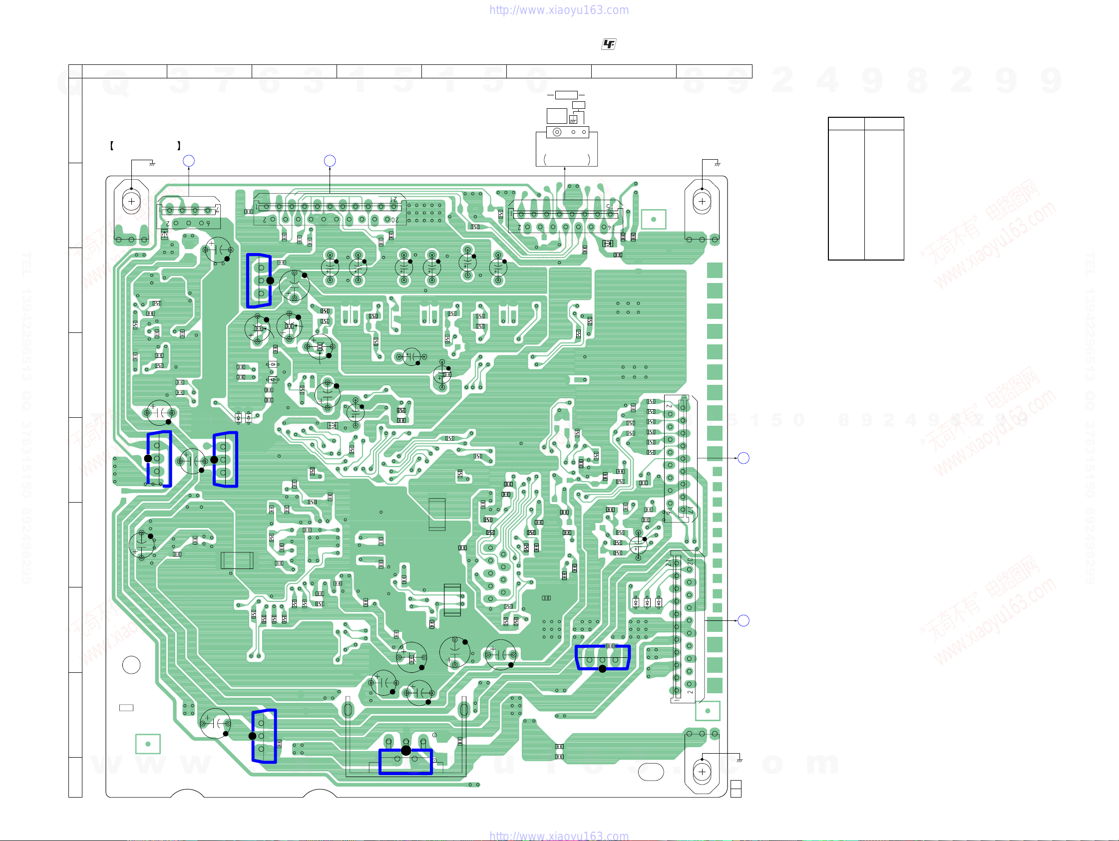
4-5. PRINTED WIRING BOARD – DIGITAL Board (Conductor Side) –
1 2 3 4 5 6 7 8
Q
Q
3
7
6
3
1
A
DIGITAL BOARD
(CHASSIS)
B
G1101
TEL 13942296513 QQ 376315150 892498299
R1317
C1313
E
IC1071
L
1525
C
C1312
R1314
C1064
C
D
T
E
F
G
(CONDUCTOR SIDE)
A
CN197
1308
FB
R1318
C1315
C1308
C1314
C1310
C1309
1
3
1
C1914
C1519
C1520
MAIN BOARD
CNS301
3
(Page 20)
C1306
C1657
C1658
9
IC1902
C1569
3
1
JR2002
IC1001
1004
D
4
1003
D
1
3
C1656
C1674
C1510
1514
R
1546
R
C1514
C1513
C1654
1545
R
2
C1003
C1004
1574
R
D1661
D1600
1567
C
C1670
1573
R
C1002
C1673
2
C1501
R
R
R1512
C1509
1572
R
C1568
510
1513
C1511
C1508
1001
C
C1671
1571
R
1487
C
C1672
9
B
CNS191
C1418
C1653
FB1453
R1570
MAIN BOARD
R1422
R1420
6
C1503
CNS403
C
C1457
C1507
C1506
1458
R1556
C1547
5
C1505
(Page 20)
R1423
1421
R
1
C1504
C1516
C1906
• See page 11 for Circuit Boards Location.
5
C1566
1448
C
C1402
3
C1517
C1518
R1492
C1456
C1502
C1127
C1908
C
1438
R1044
1
1471
R
C1460
JR2000
1049
R
C1138
C1515
R1261
R1442
C1450
R1043
JR2001
C1428
C1299
R1636
R1635
5
1260
R
C1468
R1441
R1461
C1620
C1022
C1605
R1051
R1050
R1039
1190
R
C1604
0
1052
C1101
R
ANTENNA
FM 75Ω
COAXIAL
TN1
TUNER
SUPPLIED WITH THE
ASSEMBLED BLOCK
CNS195
C1251
1167
R
Q
Q
C1142
C1121
C1102
C1130
AM
C1129
FB1351
1097
R
C1120
IC1904
: Uses unleaded solder.
1280
C1281
C
C1282
R1169
R1071
C1139
R1072
R1073
C1021
R
C1125
R1175
R1058
1096
R1158
3
R1159
R1059
13
C1100
R1201
C1066
C1068
6
7
R1088
R1180
R1179
C1065
C1067
C1069
1108
1110
1107
D
D
D
CN
S193
CNS
8
3
194
G1102
(CHASSIS)
1
9
5
D
DISPLAY
BOARD
CNS151
(Page 22)
C
MAIN
BOARD
CNS822
(Page 20)
1
2
5
0
4
• Semiconductor
9
Location
Ref. No. Location
D1003 E-2
D1004 E-2
D1107 G-7
D1108 G-7
D1110 G-7
D1600 D-3
D1661 D-3
IC1001 C-3
IC1031 H-3
IC1071 E-1
IC1901 I-4
IC1902 E-2
IC1904 G-7
9
8
2
8
4
9
2
8
2
9
9
9
TEL 13942296513 QQ 376315150 892498299
9
H
STR-KS500
I
w
w
IC1031
C1032
w
3
1031
.
C
1
x
i
a
15
24
IC1901
o
C1905
y
u
1
C1804
C1805
6
3
.
G1000
(CHASSIS)
c
1-870-403-
o
11
(11)
m
1313
STR-KS500
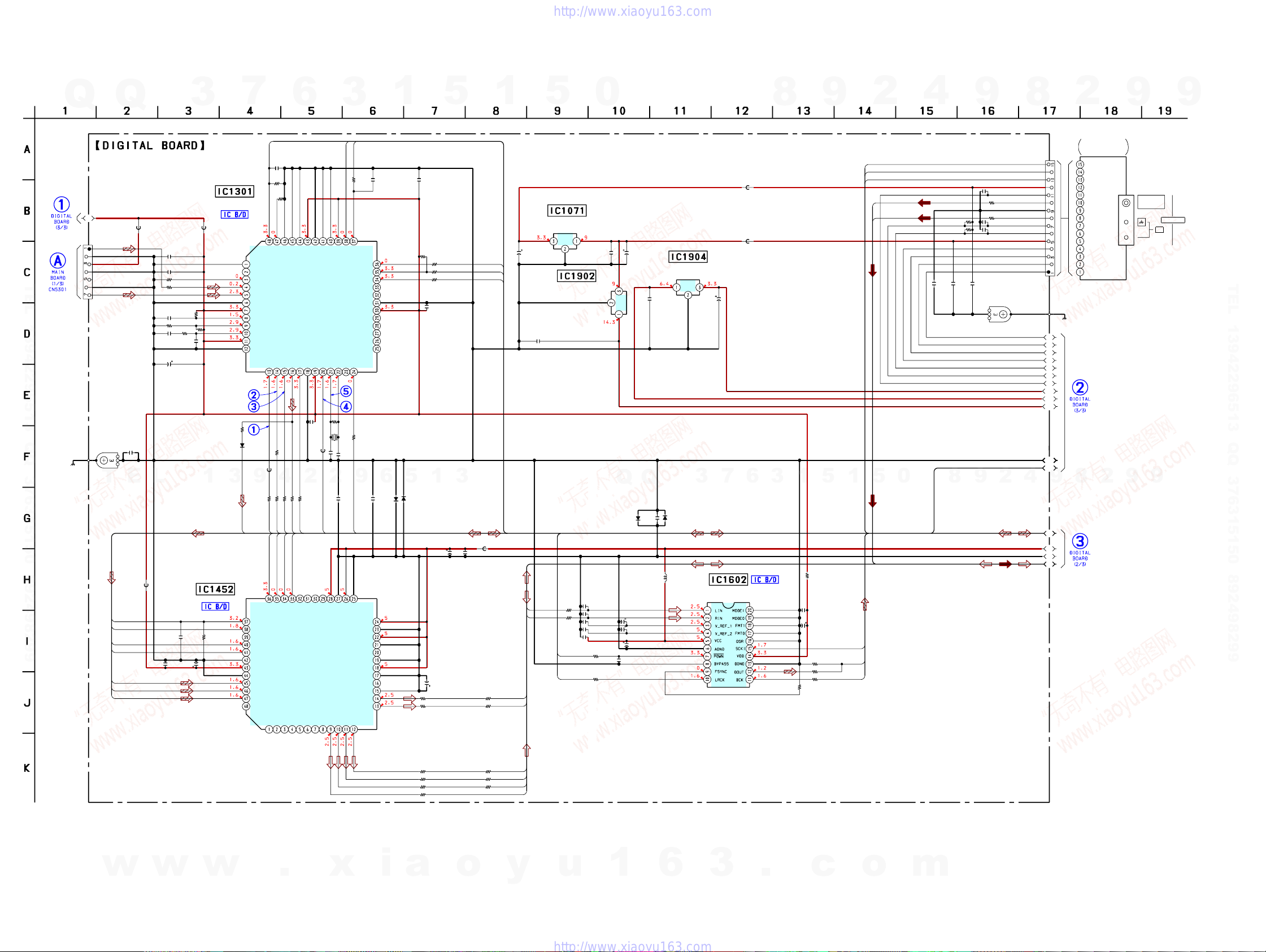
4-6. SCHEMATIC DIAGRAM – DIGITAL Board (1/3) –
DIGITAL AUDIO
INTERFACE RECEIVER
R1308
100
D1301
1SS352
3
7
DISEL
DOUT
DIN0
DIN1
DIN2
D.GND
DVDD
R
VIN
LPF
AVDD
AGND
FB1301
9
R1305
470
DATAO
RST
SCKI
SCKO
BCK
LRCK
TEST
VDD
DGND
DATA1
DATA2
DATA3
ZER0A
C1315
XMODE
R1318
R1317
XMODE
CKOUT
KFSIO
PCM_ML
ML
ZER01
0.1
10k
10k
100
1360
R
0
1020
JR
BCKI1
PCM_MC
CKSEL1
BCK
4
MC
ZER02
CKSEL0
LRCK
22
1306
R
LRCKI1
PCM_MDI
MDI
ZER03
Q
Q
3
(1/3)
B2
FB1308 FB1302
(Page 16)
TEL 13942296513 QQ 376315150 892498299
(Page 17)
(CHASSIS)
CN197
SACD-IN
GND
+3.3V
GND
+5V
GND
COAX-IN
7P
G1101
T
PCM_RST
SCKOUT
BCKO
LRCKO
SDO2
SDO3
SDO1
C1131
0.1
E
FB1453
L
47 16V
C1454
0.1
0.1
C1301
0.1
C1305
100
R1362
100
R1361
R1301C1302
5.6k0.01
33k
R1303
4.7k
R1302
R1304C1303
1000.1
C1304
C1306
0.01
1
D/A CONVERTER
R1492C1456
10k0.1
C1457
10
50V
• See page 24 for Waveforms. • See page 24 for IC Block Diagrams.
6
DOSEL0
DOSEL1
LC89056W
XSTATE
DATAO
100
100
2
1307
1309
R
R
XSTATE
SDI2
PCM_MDO
NC
MDO
IC1452
PCM1602APT
ZER05
ZER04
3
CE
CLK
C1313R1316 C1314
100p100 0.1
CE
CLK
XSEL
DVDD
DGND
MODE0
MODE1
DGND
XOUT
XMCK
DVDD
C1308
0.1
18p
1309
C
1305
FB
2
C1003
0.1
SCKI
NC
NC
NC
VCC1
ZER06
VOUT6
NC
NC
XIN
AGND1
VOUT5
DI
DO
ERROR
BPSYNC
AUTO
DGND
DVDD
F3/P3/C3
F2/P2/C2
F1/P1/C1
F0/P0/C0
CSFLAG
EMPHA
AUDIO
R1310
1M
z
H
R1311
100
1301
X
12.288M
C1310
18p
9
6
D1003 D1004
C1004
ISS367
0.022
-T3
GP8
VCC2
AGND2
VCC3
AGND3
VCC4
AGND4
NC
AGND6
VCC5
AGND5
NC
VCOM
VOUT1
VOUT2
VOUT3
VOUT4
1
5
ISS367
5
R1314
10k
R1315
100
R1313
100
R1312
100
C1312
0.1
EXLOCK
1
DI
DO
5
+3.3V REGULATOR
IC1071
TA78033LS
C1064
47
16V
+9V REGULATOR
C1913
0.1
0
IO
G
IC1902
TA7809S
C1914
C1063
0.1
47
16V
+3.3V REGULATOR
IC1904
BA33BC0T
OI
G
O
G
I
C1021
0.1
C1022
470
10V
8
FB1351
FB1352
9
2
RDS DATA
RDS CLK
RDSSIGNAL
R CH
L CH
4
R1251
9
39k
C1282C1280C1281
0.10.10.1
8
CNS195
15P
RDS DATA
RDS INT
FM SIG OUT
VDD 3.3V
C1251
0.1
MUTING
R1261
0
R CH
R1260
C1253R1252
C1252
G1102IC1301
GND
0
L CH
0.139k
STEREO
0.1
TUNED
VDD 10V
CE
DATA
DO
CLOCK
2
SUPPLIED WITH
THE ASSEMBLED
RDS DATA
RDS INT
FM SIG OUT
VDD 3.3V
MUTING
R CH
GND
L CH
STEREO
TUNED
VDD 10V
CE
DATA
DO
CLOCK
TUNER
BLOCK
9
TN1
FM 75Ω
COAXIAL
9
ANTENNA
AM
TEL 13942296513 QQ 376315150 892498299
(CHASSIS)
B3
B4
B5
B6
B7
B8
B9
B10
B11
B12
(Page 16)
B13
B14
1
3
-T3
1SS355WTE-17 1SS355WTE-17
C1460
C1450
10
FB1452
0.1
50V
R1609
470
R1618
470
1803_RST
LRCKI1
C1657
C1658
C1654
C1671
C1672
R1672
100
R510
100
L IN
R IN
C1402
10
50V
R1420
0
R1421
0
R1422
0
SL
R1423
0
SR
Q
Q
C1674
D1600 D1661
0.001
L1604
10µH
0.01
0.01
C1656
0.1
0.1
0.1
10 50V
C1670
10 50V
C1673
47 10V
C1675
0.01
3
7
A/D CONVERTER
IC1602
PCM1803DBR
6
3
1
L1605
C1659
C1653
R1671
0
1
5
0
0.1
10
50V
SCKI
R1608
2.2k
SDI1
R1607
1k
R1606
100
BCKI1
5
0
8
9
2
4
9
A1
A2
A3
A4
8
(Page 15)
2
9
9
STR-KS500
w
w
w
.
x
i
a
R1460
0
R1461
0
R1471
0
R1470
0
o
R1440
R1441
R1442
0
C
0
SW
0
FL
FR
y
u
1
6
3
.
c
o
m
1414

STR-KS500
4-7. SCHEMATIC DIAGRAM – DIGITAL Board (2/3) –
Q
Q
3
7
6
3
• See page 24 for Waveforms. • See page 27 for IC Pin Function Description.
1
(2/3)
C1514 C1510C1513
0.1 0.10.1
R1514 C1509
2
VDDI
VSS
0
0
1
8
0
5
1
R
HACN
TST3
HACN
10k 0.1
TST2
GP11
9
HCLK
HDIN
0
0
1
9
0
5
1
R
HDOUT
HCLK
HDIN
SYNC
HDOUT
6
HCS
SDI3
SDI4
GP12
HCS
GP12
PM
R1512
10k
C1501
13.9MHz
27p
R1523
R1513
R1502
R1503
R1504
R1505
R1506
3
C1511
0.1
0.1
220
10k
FB1503R1556
100
220
9
4
100
100
100
2
VSS
XRST
EXTIN
LRCKI3
VDDI
BCKI3
PLOCK
VSS
MCLK1
VDDI
VSS
MCLK2
MS
SCKOUT
LRCKI1
VDDE
BCKI1
SDI1
LRCKO
BCKO
VSS
KFSIO
SDO1
SDO2
SDO3
SDO4
SPDIF
LRCKI2
BCKI2
SDI2
TEL 13942296513 QQ 376315150 892498299
100
R1515
R1501
1M
X1502
1
C1522
C1521
27p
100
T
XRST
SCKOUT
SDI1
LRCKO
BCKO
E
KFSIO
SDO1
SDO2
SDO3
LRCKI1
BCKI1
SDI2
C1503
0.1
L
A10
A11
A0
A1
PM
VSS
AUDIO DIGITAL SIGNAL PROCESSOR
5
1
GP14
GP13
VSS
VDDI
5
A9
D8
A2
GP15
OE
D0
OE0
D9
CXD9862R
3
CS
1
D13
D12
D11
D10
D5
D4
D3
D1
D2
VDDE
IC1501
WMD0
VSS
WMD1
VDDE
WE0
CS0
0
2
2
1
4
5
1
R
WE
C1504 C1506 C1505
0.1 0.1 0.1
VSS
PAGE2
5
A6
A7
D14
D15
A3
D7
D6
VDDI
BOOT
PAGE0
PAGE1
VSS
R1529
220
0
A1
A5
A0
D8
A8
A7
A6
A5
A4
TST1
BST
BST
MOD1
MOD0
EXLOCK
EXLOCK
VSS
XTRST
VDDI
TCK
TMS
TDO
A10
A11
A12
VSS
D10
D11
VDDE
D12
D13
D14
D15
VSS
VDDI
Q
GP8
GP9
GP10
A13
A14
A15
A16
A17
VSS
10k
C1507
R1511
R1574
R1573
R1572
R1571
R1570
3
10k
10k
10k
10k
0.1
7
100
TDI
A9
D8
D9
Q
6
C1519
0.1
C1520
0.1
C1508
0.1
8
A12
A13
A14
A15
D7
D6
D5
D4
D3
D2
D1
D0
3
GP8
GP9
A2
A4
A3
1
A4
A3
A2
A1
A0
CS
D0
D1
D2
D3
D4
D5
D6
D7
WE
A15
A14
A13
A12
9
C1502
0.1
5
R1528
R1527
R1544
R1545
R1546
R1555
R1543
R1542
R1540
R1539
R1538
R1537
R1536
R1535
R1547
R1534
R1533
R1532
1
C1001
220
220
220
220
220
220
220
220
220
220
220
220
220
220
220
220
220
220
470
10V
2
S-RAM
5
+5V REGULATOR
TA7805S
IC1001
0
G
4
IC1502
IS61WV6416BLL
IO
C1002
0.1
8
SW
R IN
L IN
FL
FR
SR
R CH
L CH
SL
C
9
C1525
100
10V 0.1
9
C1516
2
8
R1520
R1521
R1522
R1557
R1519
R1518
R1517
R1554
R1553
R1552
R1525
R1526
R1551
R1550
R1549
R1548
C1515
470
10V 0.1
4
C1468
C1472
01050V 1k
C1438
R1445C1441
10 50V
00
C1448
R1484C1483
10 50V
00
C1458
R1425C1422
10 50V
00
C1418
R1464C1462
10 50V
00
C1428
R1435C1432
10 50V
00
C1518
220
220
220
220
220
220
220
220
220
220
220
220
220
220
220
220
9
R1476
R1446
R1486
R1466
R1426
R1436
C1517
1k
1k
1k
1k
1k
470
10V
2
A5
A6
A7
OE
D15
D14
D13
D12
D11
D10
D9
D8
A8
A9
A10
A11
8
C1487
C1568
C1566
C1547
C1567
C1569
2
0.0022
0.0022
0.0022
0.0022
0.0022
0.0022
9
FB1501
FB1502
9
9
CNS191
LATCH
CLOCK
TUNER-R
TUNER-L
9
TEL 13942296513 QQ 376315150 892498299
(Page 16)
C1
C2
C3
C5
C6
21P
DATA
-7V
SW
+7V
R
GND
L
GND
L
GND
R
GND
SR
GND
SL
GND
C
A3
A4
A2
A1
(Page 16)
(Page 17)
(Page 14)
STR-KS500
w
w
w
.
x
i
a
o
y
u
1
6
1515
3
.
c
o
m
STR-KS500
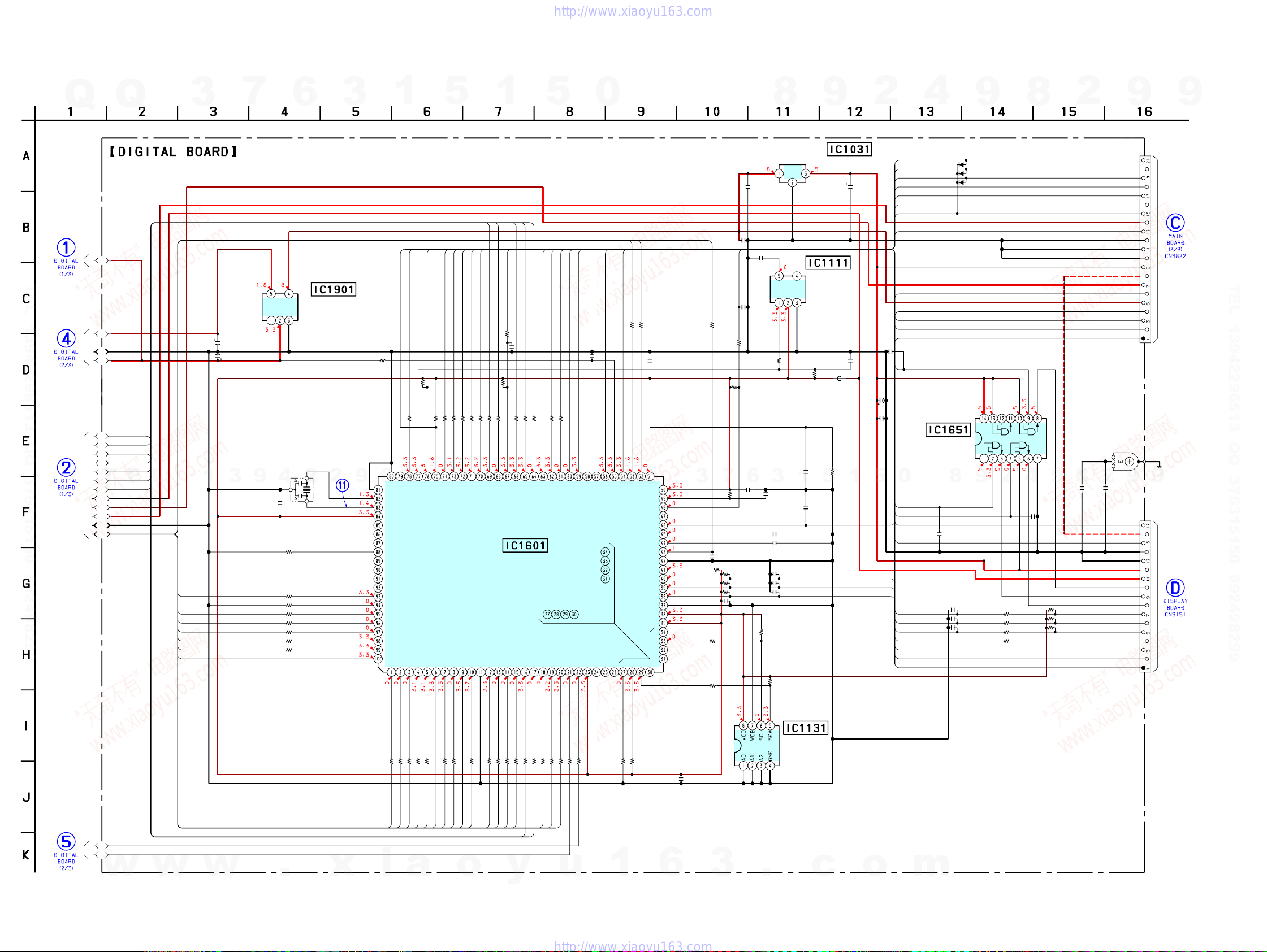
4-8. SCHEMATIC DIAGRAM – DIGITAL Board (3/3) –
Q
Q
3
7
• See page 24 for Waveforms. • See page 27 for IC Pin Function Description.
6
3
(3/3)
B2
TEL 13942296513 QQ 376315150 892498299
(Page 14)
+1.85V/+3.3V
REGULATOR
GONC
R1049
R1041
R1043
R1140
R1134
R1135
R1136
R1137
2
10k
100
10k
100
100
100
100
100
IC1901
SI-3008KWF
2
9
R1201
22k
6
DATAO
X0A
VSS
X0
X1
VCC3
NOT IN USE
NC
NOT IN USE
LRCK_SW
NOT IN USE
NOT IN USE
NOT IN USE
NOT IN USE
XMODE
CKSEL1
CLK
CE
DI
DO
ERROR
XSTATE
(Page 15)
(Page 14)
C3
C1
C2
B3
B4
B5
B6
B7
B8
B9
B10
B11
B12
B13
B14
T
T_DCLK
T_DATA
SLATCH
T_TUNER
T_STEREO
E
T_MUTE
OV
C1908
47
16V
C1906
47
16V
DO
X1101
L
XMODE
CLK
CE
DI
DO
EXLOCK
XSTATE
1
3
9
C1299
24MHz
4
0.1
1
F_CLK
PWR_RY
100
R1106
5
A
1
X
GP9
Y
LA
E
R
R
E
W
O
P
T
S
B
LEVEL_DETECT
10k
R1050
T
X
T
C
S
TE
R
E
_D
EL
V
E
L
N
C
S
A
C
H
H
10k
R1051
1
5
F_CTRL2
100
R1053
2
K
L
L
C
TR
_
C
N
F_
FA
T
S
M
R
P
X
F_CTRL1
100
R1052
3
L1
TR
C
F_
2
1
P
G
R_RY
2.2k
R1110
1
DO
F_RY
C_RY
SLATCH
PROTECTOR
100
R1112
1k
2.2k
2.2k
1k
10k
R1125
R1109
R1107
R1126
R1039
Y
Y
Y
O
R
H
C
D
LA
LA
LA
T
E
T R
N
O
FR
L
_M
02
16
S
M
S
C
V
P
TO
A
L
EC
T
S
O
R
P
SYSTEM CONTROLLER
MB90488BPF-G
I
D
C
M
_M
2_
02
0
6
16
1
M
M
C
C
P
P
E
E
R
R
R
R
A
TE
E
N
R
E
C
T
T
S
S
_R
_R
2
3
0
0
16
18
M
M
C
C
P
P
T_TUNER
0.1
C1101
1k
R1119
D
E
N
TU
IC1601
-196E1
O
D
_M
2
60
1
M
C
P
T_STEREO
100
R1113
O
E
R
E
T
S
K
L
C
_
R
E
N
U
T
T_MUTE
100
R1115
FL_STB
E
T
U
M
TA
A
D
_
R
E
N
U
T
5
FL DIN
FL CLK
100
100
R1123
R1122
K
L
TB
C
_S
FL
1
2
H
H
S
S
A
FL
FLA
T
U
IN
O
D
D
H
H
IN
D
K
L
C
H
VOL A
)
(A
L
O
V
NOT IN USE
A
D
S
K
L
C
L_
O
V
VOL B
E
S
U
O
N
)
(B
L
O
V
NO USE
NO USE
A
T
A
D
L_
O
V
C1100
0.1
POW_MUTE
SCL
5
C
C
V
0
ER KEY
POW
C
EY
N
K
R
E
W
O
P
E
S
U
IG
/D
IN
T
A
O
N
A
N
FUSE DET
Q
T
C
E
ET
E D
S
FU
FAN-HI-DETECT
E
S
U
IN
T
O
N
RDS DATA
220
R1059
S
C
IR
S
RDS SIGNAL
A
T
A
D
S
D
R
RDS CLK
220
R1058
Q
K
L
C
S
D
R
NO USE
VERSION
MODEL
STOP
AVSS
AVRH
AVCC
9
R1179
R1180
R1088
2
HIGH SPEED DETECT
8
C1085
0.1
10k
10k
10k
FRONT SP RELAY
CENTER SP RELAY
REAR SP RELAY
LEVEL_DETECT
PROTECTOR
STANBY+V
DIGITAL+V
POWER RELAY
2
C1084
0.1
+3.3V(STBY)
VOL UP(2A)
VOL DOWN(2B)
POWER ON/OFF
CNS194
F_CTRL2
F_CTRL1
G1000
CNS193
FL CLK
FL DATA
21P
F_CLK
17P
FL LAT
SIRCS
9
+V
GND
GND
GND
NC
-30V
F2
F1
STOP
9
F1
-30V
F2
GND
GND
+5V
AD2
AD1
AD0
(CHASSIS)
9
9
(Page
19)
(Page
23)
TEL 13942296513 QQ 376315150 892498299
F_RY
C_RY
R_RY
LEVEL_DETECT
F_CTRL2
F_CTRL1
PROTECTOR
F_CLK
F2
F1
STOP
PWR_RY
HI-DEC
FL_STB
0
FL CLK
FL DIN
F1
F2
VOL A
VOL B
POWER KEY
FUSE DET
AD2
AD1
AD0
4
LEVEL SHIFT
TC74VHCT08AFT
C1066
220p
IC1651
8
C1130
C1129
C1102
9
D1110
D1107
D1108
V
9
0.01
0.01
0.1
ISS352
1SS352
1SS352
2
R1186
R1105
R1129
R1124
8
G
4
C1065
220p
10k
10k
100
100
C1032
1
2
470
10V
C1067
220p
C1069
10
50V
C1068
0.1
5
AD2
AD1
AD0
8
IC1031
BA50BC0T
C1031
0.1
C1905
0.1
C1137
STOP
0.01
RDSSIGNAL
220
R1175
100
1128
R
C1138
0.1
R1635
7
3
R1147
R1157
10k
C1120
0.01
R1070
R1073
R1072
R1071
C1142
0
0
MD2
MD1
MD0
VSS
A/D3
A/D2
A/D1
A/D0
CD NC
OVG
C1108
0.1
R1127 R1189 C1107
100 10k 0.1
R1190
10k
C1605
C1620C1604
3
6
0.10.1
C1127
C1121
C1125
10k
C1122
10k
C1123
10k
C1124
10k
0.1
R1158
3.3k
R1159
3.3k
9
+5V REGULATOR
OI
G
RESET SIGNAL
GENERATOR
IC1111
S-80929CNMC
FB1101
R1636
10k
0.1
5
1
0.1
HI-DEC
0.1
0.1
0.1
0.1
0.1
(Page 15)
STR-KS500
C5
C6
w
w
w
.
x
i
100
R1044
DATAO
100
100
R1142
R1143
BST
GP9
a
100
R1144
HCS
100
R1149
HACN
100
100
100
100
100
100
100
100
100
100
100
100
100
100
1162
1161
R1150
R1121
R1151
R1156
R1152
R1153
R1154
R1168
R1167
R
_MDI
PM
XRST
PCM_RST
GP12
1803_RST
o
PCM_ML
PCM_MC
PCM_MDO
PCM
y
T_CLK
T_DATA
HDOUT
R
R1160
HCLK
HDIN
u
R1163
1169
R
100K
1097
R
1
10K
1096
R
C1139
6
0.1
3
.
EEPROM
IC1131
BR24L16
c
o
m
1616
STR-KS500
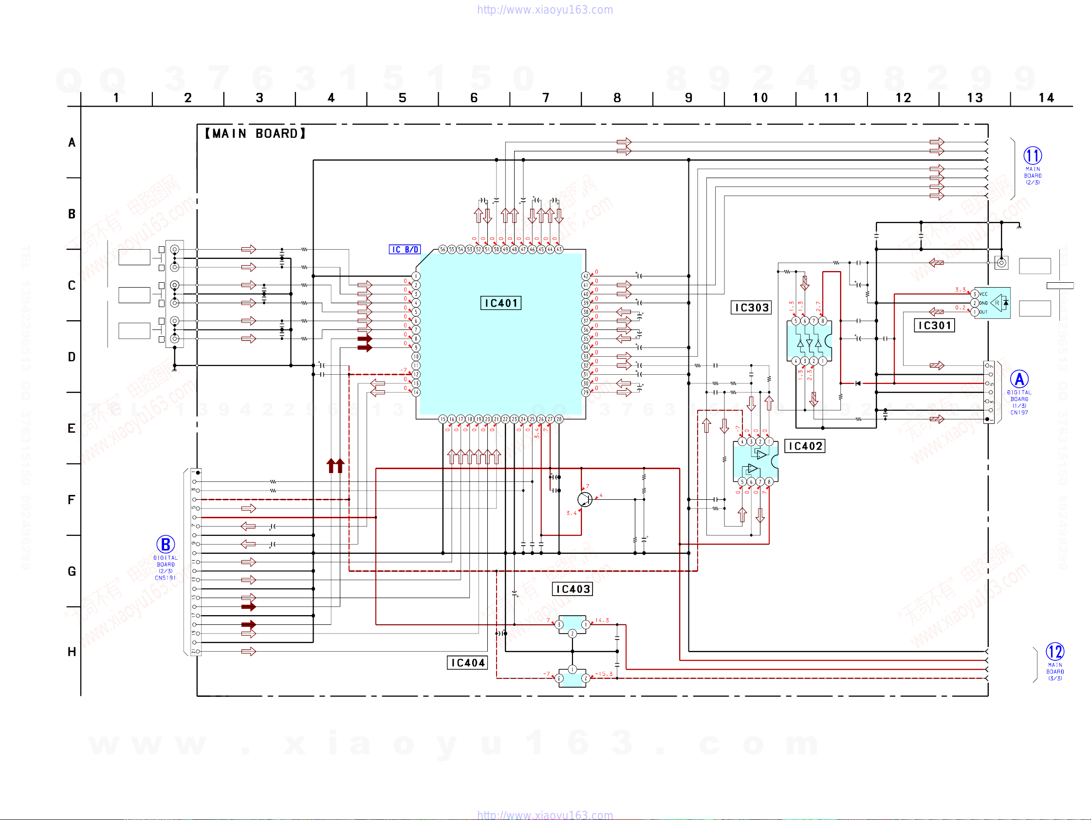
4-9. SCHEMATIC DIAGRAM – MAIN Section (1/3) –
3
7
9
4
6
CC52 CC01
100P 100P
2
CC03
100P
CC53CC02
100P100P
CC51
100P
2
Q
Q
TEL 13942296513 QQ 376315150 892498299
SA-CD/CD
AUDIO IN
VIDEO 1
J1710
6P
AUDIO IN
VIDEO 2
AUDIO IN
T
E
L
3
L
R
L
R
L
R
(CHASSIS)
1
• See page 24 for IC Block Diagrams.
C465
C464
1
220
10V
0.1
6
3
(1/3)
R403
1k
R453
1k
R402
1k
R452
1k
R401
1k
R451
1k
9
5
1
5
3
1
GND
INL5
INR5
INL4
INR4
INL3
INR3
INL2
INR2
INL1
INR1
AVEE
ADIFL
ADIFR
5
C491
4.7
50V
2
2
1
1
O
L
L
R
R
IG
C
C
C
C
L
E
E
E
E
R
R
R
R
AUDIO SELECTOR,
ELECTRICAL VOLUME
D
IN
N
G
IN
IN
R
L
IN
L
R
S
S
50V
2.2
C481
IN
V
L
IC401
M61542FP
IN
C
C
V
L
IN
W
S
0
T
U
O
L
D
N
G
1
R376
1k
9
C590
0.33
C592 R595
0.68 5.6k
5
8
50V
2.2
C476C493
4.7
4.7
50V
50V
C480
T
C
O
O
IN
U
V
O
R
R
D
N
TA
G
A
D
D
Q
IN
V
V
IG
IG
R
R
R
R
S
S
SRC
SROUT
SLOUT
SLC
SLVIN
SLIGO
CIGO
CVIN
CVC
COUT
SWOUT
SWC
SWVIN
SWIGO
K
D
C
C
D
D
C
O
V
N
L
V
C
D
A
Q
G
3
7
C479
C477
C478
4.7 50V
C475
4.7 50V
C474
C496
C473
C472
4.7
50V
6
2.2 50V
2.2 50V
2.2 50V
4.7 50V
2.2 50V
3
R593R594
56k10k
1
INVERTER
IC303
TC7WU04F
(TE12R)
C594
0.22
2
R591
2.2k
5
0
R305
47k
4
D
N
G
8
0.1
22
25V
75
0.1
-17
100
2
8
C304 C303
0.1 0.001
C301
0.1
C308
47p
4
9
C306
R304
470
C305
R303
C
C310
C
V
C309
1000
6.3V
D301
1SS355WTE
R306
470k
R307
9
9
2
DIGITAL OPTICAL
RECEIVER
IC301
TORX147L(SONY)
8
2
SACD-IN
COAX-IN
9
CNS301
7P
GND
+3.3V
GND
+5V
GND
9
L CH
R CH
GND
C CH
SW CH
SR CH
SL CH
9
9
(Page 18)
(CHASSIS)
(Page 14)
J301
DVD
COAX IN
IC301
SA-CD/CD
OPT IN
TEL 13942296513 QQ 376315150 892498299
1P
DIGITAL
(Page 15)
CNS403
21P
LATCH
CLOCK
DATA
-7V
SW
+7V
R
GND
L
GND
L
GND
R
GND
SR
TUNER-R
GND
TUNER-L
SL
GND
C
R481
R482
C403
C402
100
100
10 50V
10 50V
-7V REGULATOR
IC404
TA79007S
C443
R596
8.2k
C487
10
50V
C488
0.1
100p
100p
C489
C490
C467
0.1
C442
100
10V
100
10V
+7V REGULATOR
IC403
TA7807S
2SC3661
+3.3V
REGULATOR
IGO
IGO
Q401
C440
C441
R472
1k
R471
680
C466
R475
2.2k
0.1
0.1
220
10V
C593
0.022
R597
470k
EE
V
LINE AMP
C
VC
IC402
NJM4565M(TE2)
CHASSIS GND
+7V
AUDIO +
AUDIO -
(Page 19)
STR-KS500
w
w
w
.
x
i
a
o
y
u
1
6
1717
3
.
c
o
m
STR-KS500
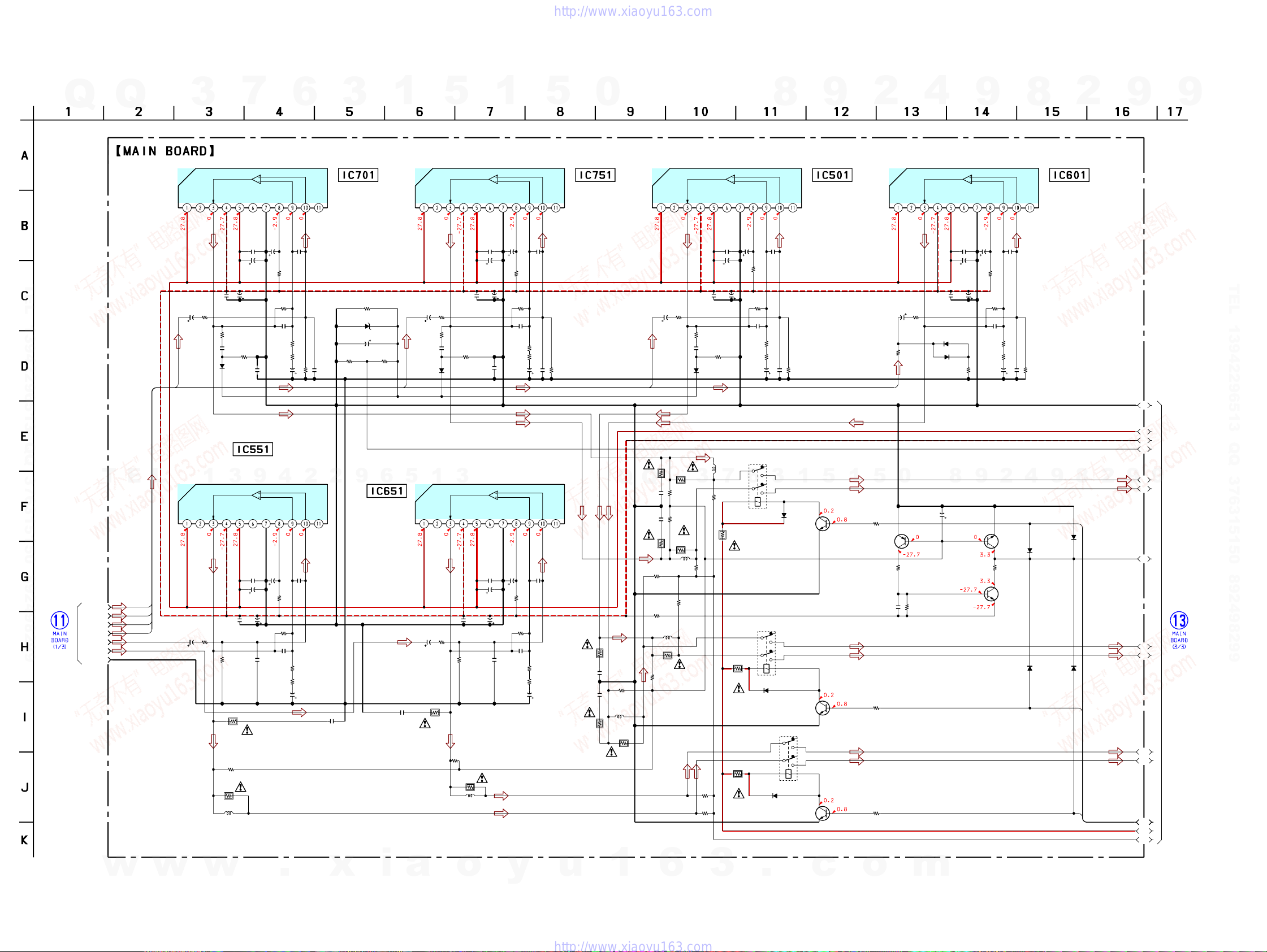
4-10. SCHEMATIC DIAGRAM – MAIN Section (2/3) –
Q
Q
3
7
(2/3)
6
3
1
5
1
5
0
8
9
2
4
9
8
2
9
9
MUTE
GNDNCV+V-NCV+ NC
C707
0.1
C718
50V
R715
C706
33k
1
TEL 13942296513 QQ 376315150 892498299
C701
R701
4.7
100
50V
L CH
T
E
(Page 17)
SW CH
SR CH
SL CH
L
SW CH
L CH
R CH
C CH
L CH
R CH
C CH
GND
1
V+ NC V- V+ NC GND
C651
R651
4.7
100
50V
50V
R705
C710
C708
1 50V
0.1
R529
10k
R539
C529
100k
0.01
D529
1SS355WTE
-17
C705
0.0022
POWER AMP
IC551
LM3886T
3
1 50V
C660 C658
0.1 1 50V
R652 C652
22k 100p
R659 C661
10 0.022
R658
47k
R657
4.7
L657
22k
C704
27p
R703
1k
R704
330
C709
100 10V
9
4
MUTE
C657
C668
0.1
50V
R665
33k
C656
C654
5p
R653 R533
1k 1k
R654
330
C659
100 10V
NC
C703
1
0.001
22k
100p
R702
C702
2
NC NC
1
C653
560p
R655
22k
IC701 IC751 IC501 IC601
LM3886T LM3886T LM3886T LM3886T
R840
10k
D841
UDZSTE-175.6B
C842
47 25V
R844
2
R843
22k
4.7k
9
6
POWER AMP
IC651
C581
0.022
R CH
5
D549
1SS355WTE
-17
C751
4.7
50V 100
R549
10k
C549
0.01
1
C531
4.7
50V
R589
MUTE
GNDNCV+V-NCV+ NC
C757
0.1
C768
C753
1
0.001
50V 560p
R765
C756
1 50V
33k
MUTE
GNDNCV+V-NCV+ NC
C507
C518
0.1
50V 560p
R515
C506
1 50V
33k
MUTE
GNDNCV+V-NCV+
C607
C618
C606
1 50V
0.1
1
50V
R615
33k
C503
1
POWER AMPPOWER AMPPOWER AMPPOWER AMP
C603
TEL 13942296513 QQ 376315150 892498299
L707
7
R505
22k
C504R729
5p10k
R503
1k
100p
22k
R504
330
C502
RY701
RY501
-1
-2
D520
3
D720
1SS355WTE-17
RELAY DRIVE
-1
-2
RY601
R502
Q520
2SC3052
1
5
2SC3052
RELAY DRIVE
RELAY DRIVE
Q720
2SC3052
1
Q620
C509
100 10V
-1
6
-2
R740
47
R540
47
1SS355WTE-17
R640
47
R722
2.2k
Q731
2SA1163
R622
2.2k
5
R522
2.2k
C601
R530
1k
SW CH
0
R731
10k
AC POWER PROTECTOR
C732 R732
0.1 33k
R601
1004750V
D449
1SS355WTE-17
D448
1SS355WTE-17
8
C730
220
10VLM3886T
Q730-732
R755
C537
0.1
C536
1 50V
22k
C758C760
1 50V0.1
C754
27p
R753
100p
22k
1k
R754
330
C752
C759
100 10V
R752
Q
MUTE
GNDNCV+V-NCV+
C548
1
C533
560p
50V
R545
33k
R535
22k
R509
10
C511
0.022
C611
0.022
R608
47k
L607
R609
10
R607
4.7
C539
100 10V
C534
5p
R534
330
R751
R550
100k
C755
0.0022
3
C540 C538
R531
100
0.1 1 50V
R532 C532
22k 100p
10
R581
47k
R587
4.7
L587
R709
10
Q
C761
0.022
R759
10
C501
R501
4.7
50V
CH
C
R707
C510 C508
0.1 1 50V
100
C729
R742
0.01
100k
D729
1SS355WTE
-17
4.7
3
R708C711
R710
47k0.022
27k
R758
47k
R757
4.7
R610
L757
27k
R760
27k
R510
27k
R750
1k
L507
R507
4.7
R508
47k
R582 D620
27k 1SS355WTE-17
R660
27k
R605
22k
C608C610
1 50V0.1
C604
5p
R603
1k
100p
22k
R604
330
C602
2
D521
1SS355WTE-17
Q730
2SC3052
Q732
2SC2713
R602
4
9
D731
1SS355WTE-17
D721
1SS355WTE-17
D621
1SS355WTE-17
A1
A2
A3
A4
A5
9
9
2
8
F.RY
A6
A7
A8
A9
(Page
19)
C.RY
A10
A11
S.RY
A12
A13
A14
C609
100 10V
R536
33
9
R730
6.8k
STR-KS500
w
w
w
.
x
i
a
o
y
u
1
6
1818
3
.
c
o
m
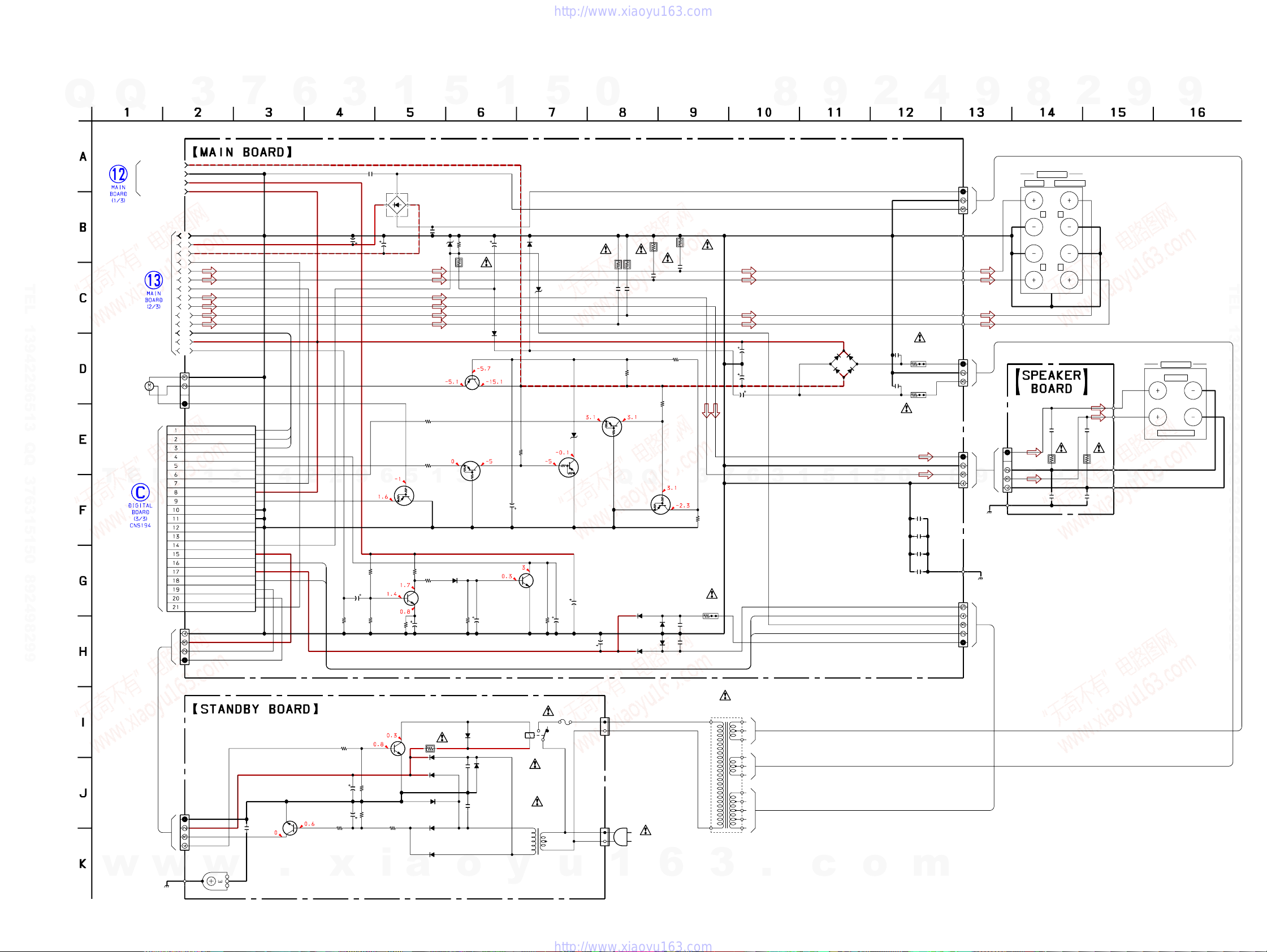
4-11. SCHEMATIC DIAGRAM – MAIN Section (3/3) –
Q
Q
3
7
6
3
1
5
1
5
0
8
9
2
4
9
8
2
STR-KS500
9
9
(3/3)
C801
0.22
2
1
CHASSIS GND
AUDIO +
AUDIO -
+7V
(Page 17)
C818
4700
2
R558
100k
50V
9
C561
4.7
50V
A1
A2
A3
A4
A5
L
A6
A7
A8
A9
A10
A11
A12
A13
A14
CNP861
CNS822
FRONT SP RELAY
CENTER SP RELAY
REAR SP RELAY
LEVEL_DETECT
F_CTRL2
F_CTRL1
PROTECTOR
+V
F_CLK
GND
GND
GND
NC
-30V
STANBY+V
F2
DIGITAL+V
F1
STOP
POWER RELAY
HIGH SPEED DETECT
21P
3P
1
CN820
F.RY
C.RY
S.RY
3
9
4
2
F2
F1
4P
TEL 13942296513 QQ 376315150 892498299
(Page 18)
M1
(FAN)
T
E
(Page 16)
3
C819
4700
50V
FAN MOTOR ON/OFF SWITCH
6
Q866
DTA124EKA
LEVEL SHIFT
R556
R554
68k
820
5
4
Q861
2SB734
C562
D809
D5SBA20
C802
0.22
D812
UDZSTE
-1730B
R886
100
R885
100
1
R553R555R557
10k4.7k220k
1SS355WTE-17
Q550
2SC3052
1
50V
FAN MOTOR LEVEL DETECT
R832
22k
R831
220
ISR154-400
Q863
DTA124EKA
3
D550
R552
3.3k150V
Q550,551
C820
100
50V
D811
FAN MOTOR CONTROL SWITCH
Q551
2SC3052
C563
Q862,863
R884
47k
C871
100
16V
D810
ISR154-400
UDZSTE-176.8B
D820
UDZSTE-175.6B
Q862
DTA124EKA
R551 C564
100k 4.7
TM500
CNP801
3P
+B
-B
R791 R741
4.7 4.7
R664
D813
C565
100
16V
50V
C664 C643
0.01 0.01
DTA124EKA
FAN MOTOR CONTROL SWITCH
C817
3300
16V
R643
4.7
4.7
C791
0.01
R881
1.5k
Q
DTA124EKA
Q867,868
Q868
D805
ISR154-400
ISR154-400
D808
R864
Q
ISR154-400
ISR154-400
47k
Q867
C741
0.01
C811
1000
7
25V
C812
1000
25V
C821
220
35V
3
6
F1
F2
R882
3.3k
3
R883
2.2k
D806
D807
R910
0.22
C815
0.1
C816
0.1
1
D802
ISR154-400
5
ISR154-400
ISR154-400ISR154-400
1
C813
D801
D804D803
C814
0.001
5
0.001
0
R810
CNP804
3P
0.47
1/2W
+R2
-R2
R811
0.47
1/2W
CN700
4P
C
GND
SW
GND
8
C744
390p
C794
330p
C694
330p
C844
330p
(CHASSIS)
CNP802
5P
+R3
F1
F2
-R3
9
(CHASSIS)
2
FRONT SURROUND
CN701
4P
C
GND
SW
4
GND
EP100
SPEAKERS
L
R
L
R
9
C544 C644
330p 330p
8
TEL 13942296513 QQ 376315150 892498299
TM501
SPEAKERS
CENTER
C641C642
0.010.01
R641R642
4.74.7
9
2
SUB WOOFER
9
STR-KS500
w
w
(CHASSIS)
CNP903
4P
G102
w
F901 CNP902
T1.25AL
2P
RY901
250V
T902
u
CNP901
2P
(AC IN)
1
Q951
2SC3052
POWER ON/OFF
RELAY DRIVE
R952
4.7k
C923
R951
3300
47k
16V
C924
R955
1
C925
0.1
2SC3052
AC POWER DETECT
.
50V
R956
10k
Q901
x
R954
100k
47k
i
R953
1
D952 D954
ISR154-400 ISR154-400
0.022
D953
ISR154-400
D955
ISR154-400
D956
1SS355WTE-17
D957
1SS355WTE-17
a
C922
o
D951
1SS355WTE-17
C921
0.022
TRANSFORMER
y
SUB POWER
MAIN POWER TRANSFORMER
6
T901
3
.
c
o
m
1919
 Loading...