

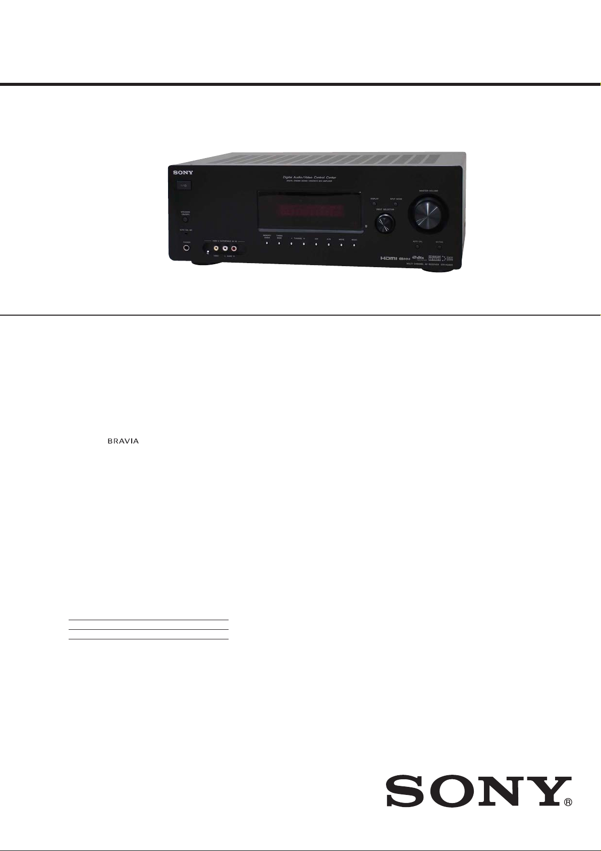
STR-KG800
SERVICE MANUAL
Ver. 1.0 2008.02
• STR-KG800 is the receiver section in
HT-DDWG800.
This receiver incorporates Dolby* Digital and Pro Logic Surround and the DTS** Digital Surround
System.
* Manufactured under license from Dolby Laboratories. Dolby, Pro Logic, and the double-D sym-
bol are trademarks of Dolby Laboratories.
** Manufactured under license under U.S. Patent #’s: 5,451,942; 5,956,674; 5,974,380; 5,978,762;
6,487,535 & other U.S. and worldwide patents issued & pending. DTS and DTS Digital Surround are registered trademarks and the DTS logos and Symbol are trademarks of DTS, Inc.
© 1996-2007 DTS, Inc. All Rights Reserved.
This receiver incorporates High-Defi nition Multimedia Interface (HDMITM) technology.
HDMI, the HDMI logo and High-Defi nition Multimedia Interface are trademarks or registered
trademarks of HDMI Licensing LLC.
“x.v.Colour” and “x.v.Colour” logo are trademarks of Sony Corporation.
“BRAVIA” and are trademarks of Sony Corporation.
AEP Model
UK Model
Amplifi er section
Power Output
Models of area code CEL, CEK
Stereo mode (rated) (6 ohms, 1 kHz, THD 1%)
90 W + 90 W
Surround mode (reference) (6 ohms, 1 kHz, THD
10%)
RMS output
FRONT:135 W
per channel
CENTER:135 W
SURROUND:135 W
per channel
1)
Measured under the following conditions:
Area code Power requirements
CEL, CEK 230 V AC, 50 Hz
2)
Reference power output for front, center and
surround speakers. Depending on the sound
fi eld settings and the source, there may be no
sound output.
1)
2)
Inputs
Analog Sensitivity: 800 mV/
50 kohms
Digital (Coaxial) Impedance: 75 ohms
Outputs (Analog)
AUDIO OUT Voltage: 800 mV/
10 kohms
SUB WOOFER Voltage: 2 V/1 kohm
Reproduction frequency range:
28 – 20,000 Hz
Tone
Gain levels ±6 dB, 1 dB step
FM tuner section
Tuning range 87.5 - 108.0 MHz
Antenna FM wire antenna
Antenna terminals 75 ohms, unbalanced
Intermediate frequency
10.7 MHz
SPECIFICATIONS
AM tuner section
Tuning range
Models of area code CEL, CEK
With 9-kHz tuning scale:
531 – 1,602 kHz
Antenna Loop antenna
Intermediate frequency
450 kHz
Video section
Inputs/Outputs
Video: 1 Vp-p, 75 ohms
COMPONENT VIDEO:
Y: 1 Vp-p, 75 ohms
PB/CB: 0.7 Vp-p, 75 ohms
PR/CR: 0.7 Vp-p, 75 ohms
80 MHz HD Pass Through
– Continued on next page –
MULTI CHANNEL AV RECEIVER
9-887-956-01
2008B05-1
2008.02
©
Sony Corporation
Audio Business Group
Published by Sony Techno Create Corporation

STR-KG800
General
Power requirements
Area code Power requirements
CEL, CEK 230 V AC, 50/60 Hz
Power output (DIGITAL MEDIA PORT)
DC OUT: 5 V, 0.7 A MAX
Power consumption
Area code Power consumption
CEL, CEK 200 W
Power consumption (during standby mode)
0.3 W (When “CONTROL
FOR HDMI” in VIDEO
menu is set to “CTRL
OFF”)
Dimensions (width/height/depth) (Approx.)
430 × 157.5 × 318 mm
including projecting parts
and controls
Mass (Approx.) 7.8 kg
Design and specifi cations are subject to change
without notice.
Notes on chip component replacement
• Never reuse a disconnected chip component.
• Notice that the minus side of a tantalum capacitor may be damaged by heat.
SAFETY-RELATED COMPONET WARNING!
COMPONENTS IDENTIFIED BY MARK 0 OR DOTTED LINE
WITH MARK 0 ON THE SCHEMATIC DIAGRAMS AND IN
THE PARTS LIST ARE CRITICAL TO SAFE OPERATION.
REPLACE THESE COMPONENTS WITH SONY PARTS
WHOSE PART NUMBERS APPEAR AS SHOWN IN THIS
MANUAL OR IN SUPPLEMENTS PUBLISHED BY SONY.
TABLE OF CONTENTS
1. SERVICING NOTES ............................................. 3
2. GENERAL .................................................................. 4
3. DISASSEMBLY
3-1. Disassembly Flow .......................................................... 9
3-2. Case ................................................................................. 9
3-3. Back Panel Block ............................................................ 10
3-4. Front Panel Block .......................................................... 10
3-5. Main Block ..................................................................... 11
3-6. MAIN Board ................................................................... 11
4. TEST MODE ............................................................ 12
5. ELECTRICAL CHECK ......................................... 14
6. DIAGRAMS
6-1. Block Diagram - MAIN Section - ................................... 15
6-2. Block Diagram - HDMI Section - ................................... 16
6-3. Block Diagram - DSP Section - ...................................... 17
6-4. Block Diagram - AUDIO Section - ................................. 18
6-5. Block Diagram - POWER SUPPLY Section - ................ 19
6-6. Printed Wiring Board - MAIN Board - ........................... 21
6-7. Schematic Diagram - MAIN Board (1/3) - ..................... 22
6-8. Schematic Diagram - MAIN Board (2/3) - ..................... 23
6-9. Schematic Diagram - MAIN Board (3/3) - ..................... 24
6-10. Schematic Diagram - DIGITAL AB Board (1/5) -.......... 25
6-11. Schematic Diagram - DIGITAL AB Board (2/5) -.......... 26
6-12. Schematic Diagram - DIGITAL AB Board (3/5) -.......... 27
6-13. Schematic Diagram - DIGITAL AB Board (4/5) -.......... 28
6-14. Schematic Diagram - DIGITAL AB Board (5/5) -.......... 29
6-15. Printed Wiring Board
- DIGITAL AB Board (Component Side) -..................... 30
6-16. Printed Wiring Board
- DIGITAL AB Board (Conductor Side) - ...................... 31
6-17. Printed Wiring Boards
- MIC/HEADPHONE Section - ...................................... 32
6-18. Schematic Diagram - MIC/HEADPHONE Section - ..... 33
6-19. Printed Wiring Board - HDMI Board (Side A) - ............ 34
6-20. Printed Wiring Board - HDMI Board (Side B) - ............ 35
6-21. Schematic Diagram - HDMI Board (1/2) - ..................... 36
6-22. Schematic Diagram - HDMI Board (2/2) - ..................... 37
6-23. Printed Wiring Boards - VIDEO Section - ..................... 38
6-24. Schematic Diagram - VIDEO Section - .......................... 39
6-25. Printed Wiring Boards - PANEL Section - ..................... 40
6-26. Schematic Diagram - PANEL Section - .......................... 41
6-27. Printed Wiring Board
- DCDC CONVERTER Board - ..................................... 42
6-28. Schematic Diagram
- DCDC CONVERTER Board - ..................................... 43
6-29. Printed Wiring Board - STANDBY Board - ................... 44
6-30. Schematic Diagram - STANDBY Board - ...................... 45
7. EXPLODED VIEWS
7-1. Front Panel Section ......................................................... 61
7-2. Back Panel Section ......................................................... 62
7-3. MAIN Section ................................................................. 63
8. ELECTRICAL PARTS LIST .............................. 64
2

SECTION 1
SERVICING NOTES
UNLEADED SOLDER
Boards requiring use of unleaded solder are printed with the leadfree mark (LF) indicating the solder contains no lead.
(Caution: Some printed circuit boards may not come printed with
the lead free mark due to their particular size)
: LEAD FREE MARK
Unleaded solder has the following characteristics.
• Unleaded solder melts at a temperature about 40 °C higher
than ordinary solder.
Ordinary soldering irons can be used but the iron tip has to be
applied to the solder joint for a slightly longer time.
Soldering irons using a temperature regulator should be set to
about 350 °C.
Caution: The printed pattern (copper foil) may peel away if the
heated tip is applied for too long, so be careful!
• Strong viscosity
Unleaded solder is more viscous (sticky, less prone to fl ow)
than ordinary solder so use caution not to let solder bridges
occur such as on IC pins, etc.
• Usable with ordinary solder
It is best to use only unleaded solder but unleaded solder may
also be added to ordinary solder.
STR-KG800
NOTE OF REPLACING THE IC1131 ON THE DIGITAL
AB BOARD
IC1131 on the DIGITAL AB board cannot exchange with single.
When IC1131 on the DIGITAL AB board is damaged, exchange
the entire mounted board.
NOTE OF REPLACING THE IC3511 AND IC3513 ON
THE HDMI BOARD
IC3511 and IC3513 on the HDMI board cannot exchange with single. When IC3511 and IC3513 on the HDMI board are damaged,
exchange the entire mounted board.
3
STR-KG800
Receiver
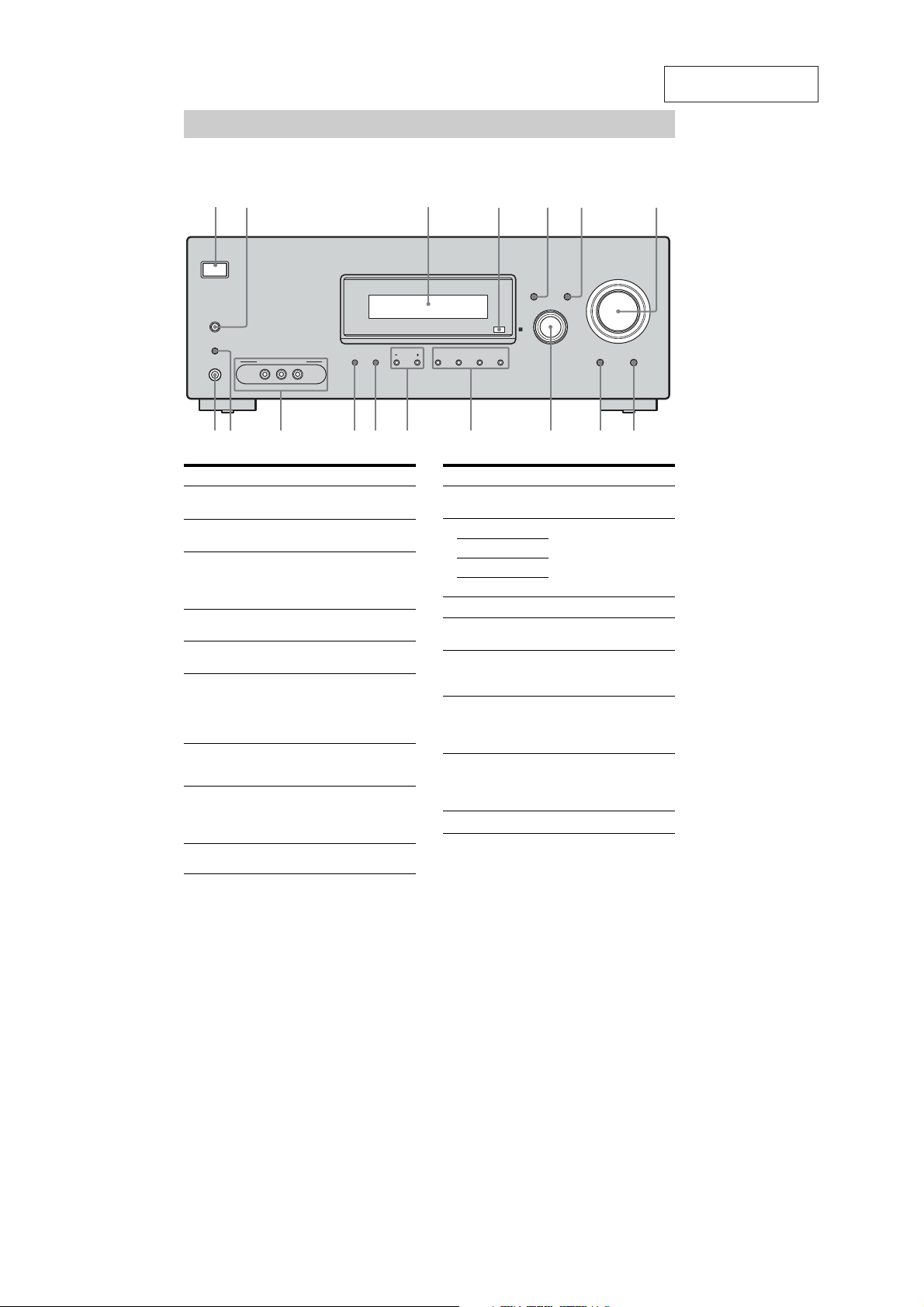
Front panel
SECTION 2
GENERAL
This section is extracted
from instruction manual.
SPEAKERS
(ON/OFF)
AUTO CAL MIC
PHONES
VIDEO 2 IN/PORTABLEAV IN
VIDEO L AUDIO R
RHRIRK
.
MEMORY/
ENTER
TUNING
TUNING 2CH A.F.D. MOVIE MUSIC
MODE
RTRERG
Name Function
" /
(on/standby)
# SPEAKERS
(ON/OFF)
$ Display The current status of the
% Remote sensor Receives signals from
& DISPLAY Press to select information
' INPUT MODE Press to select the input
( MASTER
VOLUME
) MUTING Press to turn off the sound
* AUTO CAL Press to activate the Auto
Press to turn the receiver on
or off.
Press to turn the speaker
system on or off.
selected component or a list
of selectable items appears
here.
remote commander.
displayed on the display.
mode when the same
components are connected
to both digital and analog
jacks.
Turn to adjust the volume
level of all speakers at the
same time.
temporarily.
Press MUTING again to
restore the sound.
Calibration function.
MASTERVOLUME
DISPLAY INPUT MODE
INPUT SELECTOR
MUTING
AUTO CAL
RB
R
Name Function
+ INPUT
SELECTOR
, 2CH Press to select a sound field.
A.F.D.
MOVIE
MUSIC
- TUNING +/– Press toscan a station.
. TUNING MODE Press to select the tuning
/ MEMORY/
ENTER
0 VIDEO 2 IN/
PORTABLE AV
IN jacks
1 AUTO CAL MIC
jack
2 PHONES jack Connects to headphones.
Turn to select the input
source to playback.
mode.
Press to store a station or
enter the selection when
selecting the settings.
Connects to a portable
audio/video component
such as a camcorder or
video game.
Connects to the supplied
optimizer microphone for
the Auto Calibration
function.
4
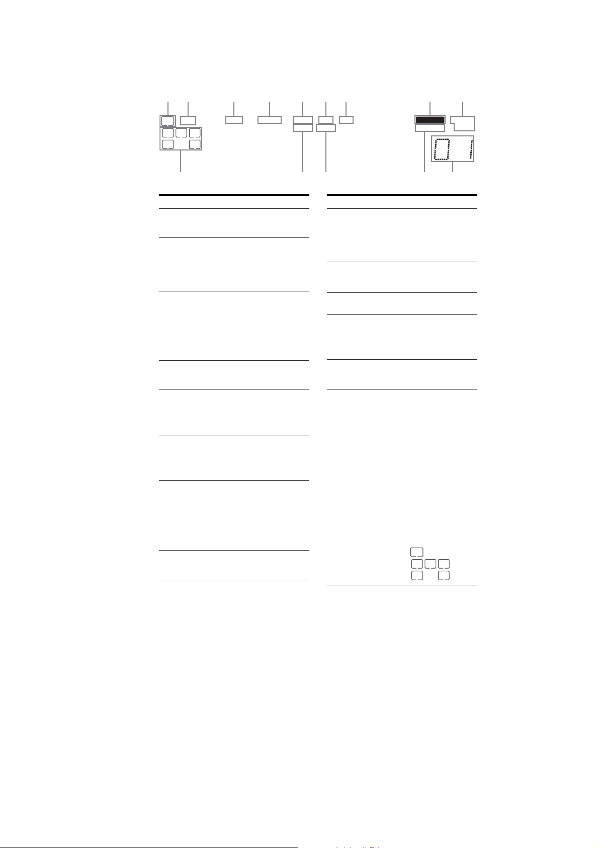
About the indicators on the display
STR-KG800
LFE
SW
LC
SL S
SR
D
R
PLII
Name Function
" SW Lights up when the audio signal
# LFE Lights up when the disc being
$ D Lights up when the receiver is
% PLII Lights up when the Pro Logic II
& PL Lights up when the receiver
' OPT Lights up when INPUT MODE
( DTS Lights up when the receiver is
) MEMORY Lights up when a memory
is output from the SUB
WOOFER jack.
played back contains an LFE
(Low Frequency Effect)
channel and the LFE channel
signal is actually being
reproduced.
decoding Dolby Digital signals.
Note
When playing a Dolby Digital
format disc, be sure that you
have made digital connections
and that INPUT MODE is set to
“AUTO” .
Movie/Music decoder is
activated.
applies Pro Logic processing to
2 channel signals in order to
output the center and surround
channel signals.
is setto “AUTO” andthe source
signal is a digital signal being
input through the OPTICAL
jack.
decoding DTS signals.
Note
When playing a DTS format
disc, be sure that you have made
digital connections and that
INPUT MODE is set to
“AUTO”.
function, such as Preset
Memory, etc., is activated.
PL OPT DTS MEMORY RDS ST
MONOD.RANGECOAXHDMI
RRBRG RTRE
Name Function
* Tuner
indicators
+ Preset
station
indicators
, D.RANGE Lights up when dynamic range
- COAX Lights up when INPUT MODE
. HDMI Lights up when the receiver
/ Playback
channel
indicators
L
R
C
SL
SR
S
Lights up when using the
receiver to tune in radio stations,
etc.
Note
“RDS” appears for models of
area code CEL, CEK only.
Lights up when using the
receiver to tune in preset radio
stations.
compression is activated.
is setto “AUTO” andthe source
signal is a digital signal being
input through the COAXIAL
jack.
recognizes a component
connected via an HDMI IN jack.
The letters (L, C, R, etc.)
indicate the channels being
played back. The boxes around
the letters vary to show how the
receiver downmixes the source
sound.
Front Left
Front Right
Center (monaural)
Surround Left
Surround Right
Surround (monaural or the
surround components obtained
by Pro Logic processing)
Example:
Recording format (Front/
Surround): 3/2.1
Sound Field: A.F.D. AUTO
SW
LCR
SL SR
5
STR-KG800
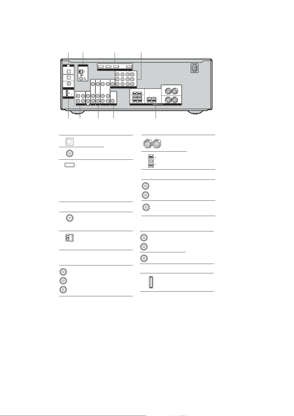
Rear panel
AM
TV
VIDEO
VIDEO
IN
AUDIO
AUDIO
IN
SAT
DVD
SAT IN DVD IN BD IN OUT
HDMI
SAT IN DVD IN VIDEO 1 IN MONITOR OUT
VIDEO
VIDEO
VIDEO
IN
IN
OUT
OUT
MONITOR
COMPONENTVIDEO
AUDIO
AUDIO
AUDIO
IN
IN
OUT
OUT
SUBWOOFER
VIDEO 1
TV
IN
IN
IN
DMPORT
(ASSIGNABLE)
DC5V
0.7A MAX
ANTENNA
OUT IN IN
L
R
SA-CD/CD/CD-R
OPTICAL
SAT
OPTICAL
DVD
COAXIAL
DIGITAL
" DIGITAL INPUT/OUTPUT section
OPTICAL IN
jacks
COAXIAL IN
jack
HDMI IN/
OUT* jacks
Connects to a DVD
player, etc. The
COAXIAL jack
provides a better
sound quality.
Connects to a DVD
player, Blu-ray disc
player, etc. The
image is output to a
TV or a projector
while thesound can
be output from a
TV or/and speakers
connected to this
receiver.
# ANTENNA section
FM
ANTENNA
jack
AM
ANTENNA
terminals
Connects to the
supplied FM wire
antenna.
Connects to the
supplied AM loop
antenna.
Y
/
P
B
C
B
PR/
C
R
SURROUND CENTER
LR
SPEAKERS
FRONT
L
R
% SPEAKERS section
& AUDIO INPUT/OUTPUT section
AUDIO IN/
White (L)
OUT jacks
Red (R)
AUDIO OUT
Black
jack
' VIDEO/AUDIO INPUT/OUTPUT
section
White (L)
Red (R)
AUDIO IN/
OUT jacks
Connects to a
VCR, DVD player,
etc..
Connects to the
supplied speakers.
Connects to a
Super Audio CD
player, etc..
Connects to the
supplied sub
woofer.
$ COMPONENT VIDEO INPUT/
OUTPUT section
Green
(Y)
Blue
(P
B/CB)
Red
(P
R/CR)
Y, PB/CB, PR/C
IN/OUT* jacks
Connects to a DVD
R
player, TV,
satellite tuner, etc.
You can enjoy high
quality image.
Yellow
VIDEO IN/
OUT* jacks
( DMPORT
DMPORT
jack
* You can watch the selected input image when you
connect the HDMI OUT or MONITOR OUT jack
to a TV.
Connects to a
DIGITAL MEDIA
PORT adapter.
6
STR-KG800
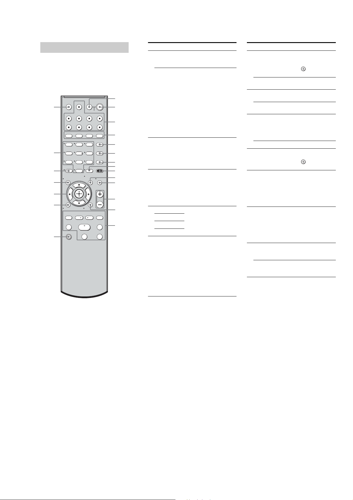
Remote commander
You can use the supplied RM-AAU023
Remote Commander to operate the receiver
and to control the Sony audio/video
components that the remote is assigned to
operate. For details, see “Changing button
assignments”.
XB
X
RM
RL
RK
RI
RH
TV INPUT
DISPLAY
RETURN/EXIT
TV CH –
PRESET –
TUNING –
SLEEP
VIDEO1 VIDEO2 BD DVD
SAT TV SA-CD/CD TUNER
2CH A.F.D.
>10
CLEAR
0
AV
SYSTEM STANDBY
MOVIE MUSIC
123
46
78
0/10
REPLAY ADVANCE
TV
THEATRE
DVD/BD
5
MENU
AUTO CAL
D.TUNING
9
D.SKIP
AMP MENU
MEMORY
ENTER
TOOLS/
MUTING
OPTIONS
TV VOL
MASTER VOL
MENU/HOME
TV CH +
PRESET +
TUNING +
)N.
FM MODE
9Y
TV
DMPORT
R
RB
RT
RE
RG
Name Function
" TV /
(on/standby)
AV /
(on/standby)
# /
(on/standby)
$ Input buttons Press one of the buttons to
% 2CH Press to select a sound field.
A.F.D.
MOVIE
MUSIC
& THEATRE Press to enjoy optimal image
Press TV / and TV (0) at
the same time to turn the TV
on or off.
Press to turn on or off the
Sony audio/video components
that the remote is assigned to
operate.
If you press / (#) at the
same time, it will turn off the
receiver and other Sony
components (SYSTEM
STANDBY).
Note
The function of the AV /
switch changes automatically
each time you press the input
buttons ($).
Press toturn the receiver on or
off.
To turn off all Sony
components, press / and
AV / (") at the same time
(SYSTEM STANDBY).
select the component you
want to use. When you press
any of the input buttons, the
receiver turns on. The buttons
are factory assigned to control
Sony components.
suited for movies and to
output the sound from the
speakers connected to this
receiver automatically.
Note
This button will only function
if your TV is compatible with
Theater Mode.
Refer to the operating
instructions supplied with the
TV for details.
Name Function
' DVD/BD
MENU
AUTO CAL Press to activate the Auto
( D.TUNING Press to enter direct tuning
D.SKIP Press to skip a disc when
) ENTER Press to enter the value after
MEMORY Press to store a station.
* AMP MENU Press to display the menu of
+ TOOLS/
OPTIONS
, MUTING Press to turn off the sound
- TV VOL
a)
/–
+
MASTER
VOL +
Press to display the menu of
the DVD or Blu-ray disc on
the TV screen. Then, use 7, W,
#, C and (2) to perform
menu operations.
Calibration function.
mode.
using a multi-disc changer.
selecting a channel, disc or
track using the numeric
buttons of the TV, VCR or
satellite tuner.
the receiver. Then, use 7, W,
#, C and (2) to perform
menu operations.
Press to display and select the
options of the DVD player or
Blu-ray disc player.
Press TOOLS/OPTIONS and
TV (0) at the same time to
display the options applicable
to the Sony TV.
temporarily.
Press MUTING again to
restore the sound.
Press MUTING and TV (0)
at the same time to activate
the TV’s muting function.
Press TV VOL +/– and TV
(0) at the same time to adjust
the volume level of the TV.
Press to adjust the volume
a)
/–
level of all speakers at the
same time.
7

STR-KG800
Name Function
. MENU/HOME Press to display the menu of
/ /
REPLAY /
ADVANCE
N/.
a)b)
)
b)
9
b)
Y
TV CH +/– Press TV CH +/– and TV (0)
PRESET +/– Press to select
TUNING +/– Press to scan a station.
FM MODE Press to select the FM
the VCR, DVD player,
satellite tuner or Blu-ray disc
player on the TV screen.
Press MENU/HOME and TV
(0) at the same time to
display the TV’s menu.
Then, use 7, W, #, C and
(2) to perform menu
operations.
b)
Press to skip a track of the CD
player, DVDplayer or Blu-ray
disc player.
Press to replay the previous
scene or fast forward the
current scene of the VCR,
DVD player or Blu-ray disc
player.
b)
Press to
– search tracks in the forward/
reverse direction of the DVD
player.
– start fast forward/rewind of
the VCR, CD player or Bluray disc player.
Press to start playback of the
VCR, CDplayer, DVD player,
or Blu-ray disc player.
Press to pause playback or
recording of the VCR, CD
player, DVDplayer or Blu-ray
disc player. (Also starts
recording with components in
recording standby.)
Press to stop playback of the
VCR, CD player, DVD player
or Blu-ray disc player.
at the same time to select
preset TV channels.
– preset stations.
– preset channels of the VCR
or satellite tuner.
monaural or stereo reception.
Name Function
0 TV Press TV and the button with
1 RETURN/
EXIT 0
2
,
7/W/#/C
3 DISPLAY Press to select information
4 -/-- Press to select the channel
>10 Press to select the track
CLEAR Press to clear a mistake when
orange printing at the same
time to enable TV operation.
Press to
– return to the previous menu.
– exit the menu while the
menu or on-screen guide of
the VCR, DVD player,
satellite tuner or Blu-ray
disc player is displayed on
the TV screen.
Press RETURN/EXIT 0
and TV (0) at the same time
to return to the previous menu
or exit the TV’s menu while
the menu is displayed on the
TV screen.
After pressing AMP MENU
(*), DVD/BD MENU ('),
or MENU/HOME (.), press
7, W, # or C to select the
settings. Then, press to
enter the selection if you have
pressed DVD/BD MENU or
MENU/HOME previously.
Press also to enter the
selection of the receiver,
VCR, satellite tuner, CD
player, DVD player or Bluray disc player.
displayed on the TV screen of
the VCR, satellite tuner, CD
player, DVD player or Bluray disc player.
Press DISPLAY and TV (0)
at the same time to display
TV’s information on the TV
screen.
entry mode, either one or two
digit of the VCR.
Press -/-- and TV (0) at the
same time to select the
channel entry mode, either
one or two digits of the TV.
numbers over 10 of the CD
player.
you press the incorrect
numeric button.
Name Function
5 Numeric
buttons
(number 5
6 TV INPUT Press TV INPUT and TV (0)
SLEEP Press to activate the Sleep
a)
The number 5, TV VOL +/MASTER VOL + and
) buttons have tactile dots. Use the tactile dots as
references when operating the receiver.
b)
This button is also available for DIGITAL MEDIA
PORT adapter operation. For details on the
function of the button, see the operating
instructions supplied with the DIGITAL MEDIA
PORT adapter.
Press to
– preset/tune to preset
a)
)
stations.
– select track numbers of the
CD player, DVD player or
Blu-ray disc player. Press
0/10 to select track number
10.
– select channel numbers of
the VCR or satellite tuner.
Press the numeric buttons and
TV (0) at the same time to
select the TV channels.
at the same time to select the
input signal (TV input or
video input).
Timer function and the
duration which the receiver
turns off automatically.
Notes
• Some functions explained in this section may not
work depending on the model.
• The above explanation is intended to serve as an
example only. Therefore, depending on the
component, the above operation may not be
possible or may operate differently than described.
8
DISASSEMBLY
• This set can be disassembled in the order shown below.
3-1. DISASSEMBLY FLOW
SET
3-2. CASE
(Page 9)
3-3. BACK PANEL BLOCK
(Page 10)
STR-KG800
SECTION 3
3-4. FRONT PANEL BLOCK
(Page 10)
Note: Follow the disassembly procedure in the numerical order given.
3-5. MAIN BLOCK
(Page 11)
3-6. MAIN BOARD
(Page 11)
3-2. CASE
two screws
(BVST4 × 8)
two screws
(BVTP3 × 8)
case
two screws
(BVST4 × 8)
9
STR-KG800
3-3. BACK PANEL BLOCK
(CN3509)
screw
(BVTP3 × 8)
(CNP912)
connector
connector
connector
RT
(CNP911)
back panel block
RE
clamp
two connectors
(CNP203, CNP204)
nine screws
R
(BVTP3 × 8)
five screws
R
(BVTP3 × 8)
two connectors
RB
(CNS501, CNS502)
three connectors
(CNP902, CNP910, CNP913)
(CNP504, CNP505, CNP512)
3-4. FRONT PANEL BLOCK
three leads (with connector)
(TP202, TP790, TP2000)
three connectors
connector
(CN790)
claw
screw
(BVTP3 × 8)
wire (flat type) (17 core)
(CNS510)
claw
10
front panel block
five screws
(BVTP3 × 8)
three connectors
(CNP430, CNP500, CNP930)
3-5. MAIN BLOCK
connector
(CN790)
three screws
(BV3)
(CNP921, CNP940)
two connectors
two screws
(BV3)
main block
STR-KG800
3-6. MAIN BOARD
screw
(BV3)
wire route board
three connectors
(CNP430, CNP500, CNP930)
ten sheets
five transistor MP1620-OPY-MK
(Q654, Q704, Q754, Q804, Q854)
Remove the
thirty solders.
ten screws
(transistor)
five transistor MN2488-OPY-MK
(Q653, Q703, Q753, Q803, Q853)
heatsink block
two screws
(BVTP3 × 8)
MAIN board
R
11
STR-KG800
SECTION 4
TEST MODE
FL CHECK MODE
All fl uorescent segments are tested. When this test is activated, all
segments turn on at the same time, then each segment turns on one
after another.
Procedure:
1. When pressing the [TUNING MODE] and [DISPLAY] buttons, press the [
] button to turn on the main power.
?/1
2. All segments turn on.
LFE
SW
L CR
S
SR
SL
SB SBRSBL
SP A
SP B
D EX
PL II xPL
OPT
HDMI COAX
DTS-ES 96 / 24
CAT
NEO:6 SAT D.RANGE
MEMORY
dB
k Hz
mft.
MHz
RDS ST
MONO
3. Turn the [INPUT SELECTOR] dial.
4. Test pattern 1 turn on.
k
m
MHz
RDS ST
MONO
LFE
L R
S
D EX
SP B
PL II x
HDMI COAX
DTS-ES
NEO:6 SAT D.RANGE
5. Turn the [INPUT SELECTOR] dial once again.
6. Test pattern 2 turn on.
SW
C
SL SR
SB SBRSBL
D
DTS
PL
CAT
MEMORY
dB
Hz
ST
ft.
7. Turn the [INPUT SELECTOR] dial once again. All segments
turn off.
8. Every turning of the [INPUT SELECTOR] dial turns on each
segment one after another on the same order.
S.F. CLEAR MODE
The preset sound fi led is cleared when this mode is activated. Use
this mode before returning the product to clients upon completion
of repair.
Procedure:
1. While pressing the [2CH] button, press the [
] button to turn
?/1
on the main power.
2. The message “S.F CLR.” appears and initialization is performed.
SWAP ALL MODE
When this mode is used, output the audio signal of front L/R channel to all channel.
Procedure:
1. While pressing the [MEMORY/ENTER] and [DISPLAY] buttons, press the [
] button to turn on the main power.
?/1
2. The message “DSP TEST” appears.
3. Press the [AMP MENU] button on the remote commander, and
the message “9_DSPTST” appears.
4. Press the [b] button on the remote commander to enter the
DSP test mode menu.
5. Press the [v] button on the remote commander twice to enter
the swap mode, and the message “SWP.AUTO” appears.
6. Press the [b] button on the remote commander twice to select
“SWP.[]ALL”.
SHIPMENT MODE
All preset contents are cleared when this mode is activated. Use
this mode before returning the product to clients upon completion
of repair.
Procedure:
1. While pressing the [SPEAKERS (ON/OFF)] and [MUSIC] buttons, press the [
] button to turn on the main power.
?/1
2. The message “CLEARING” appears.
DCAC FACTORY TEST MODE
DCAC Factory Test mode have two stages:
1. DCAC DSP Data Line Checking
2. DCAC board Checking
Start Pass Pass
DSP Data Line
Check
Auto Cal Mic
Check
END
Factory Test System Setup
Receiver
VERSION CHECK MODE
When this mode is used the model, the destination and the software
version number are displayed.
Procedure:
1. While pressing the [SPEAKERS (ON/OFF)] and [DISPLA Y] buttons, press the [
] button to turn on the main power.
?/1
2. The model, the distination and the software version number
appear.
KEY CHECK MODE
This mode is used to check the key.
Procedure:
1. While pressing the [SPEAKERS (ON/OFF)] and [2CH] buttons, press the [
] button to turn on the main power.
?/1
2. The message “REST 13” appears.
3. Every pressing of any button other than the [
] button counts
?/1
down the buttons. The buttons which are already counted once
are not counted again.
4. When all buttons are pressed, the message “REST 00” appears.
DCAC MIC
SPK Front Left
1. When power off :
While pressing the [MEMORY/ENTER] and [MOVIE] but-
tons, press the [
] button to turn on the main power.
?/1
“DCAC FTM” appears.
Afterward, press the [TUNING MODE] to start DCAC factory
test mode.
12

1. DCAC DSP Data Line Checking
After press the [TUNING MODE] button, DCAC Factory test
mode will start, below display will show:
“DCAC x” x = 1, 2, 3, 4
If there is error happen, below display will show:
“ERR SD0x” x = 1 → D1501 or R1530 problem
x = 2 → D1502 problem
x = 3 → D1503 problem
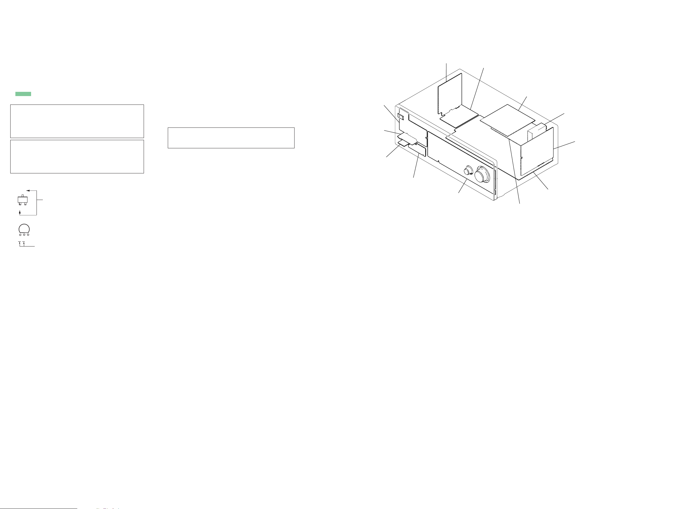
x = 4 → D1504 problem
2. DCAC board Checking
Connect front left speaker of the receiver and AUTO CAL microphone. Turn [MASTER VOLUME] jog, there will be test tone
sound output from front left speaker, and the display will change
accordingly.
“AD - xxx” xxx = 0 to 255 (depends on loudness of test tone)
RE-BOX CLASSIFICATION TEST MODE
Procedure:
1. While pressing the [MEMORY/ENTER] and [INPUT MODE]
buttons, press the [
2. The message “R.BOX[][][]XX” appears.
XX: times set powered on
] button to turn on the main power.
?/1
STR-KG800
VACS CONTROL TEST MODE
The VACS feature of the amplifi er is turned off purposely.
Procedure:
1. While pressing the [MEMORY/ENTER] and [2CH] buttons,
press the [
2. The message “VACS OFF” appears.
] button to turn on the main power.
?/1
13

STR-KG800
SECTION 5
ELECTRICAL CHECK
FM AUTO STOP CHECK
signal
generator
Procedure:
1. Turn on the set.
2. Input the following signal from signal generator to FM antenna
input directly.
Carrier frequency: A = 87.5 MHz, B = 98 MHz, C = 108 MHz
Deviation : 75 kHz
Modulation : 1 kHz
ANT input : 1 kHz
Note: Use 75 ohm coaxial cable to connect signal generator and the set.
You cannot use video cable for checking.
Use signal generator whose output impedance is 75 ohm.
3. Set to FM tuner function and scan the input FM signal with
automatic scanning.
4. Confi rm that input frequency of A, B and C are detected and
automatic scanning stops.
set
When the station signal is received in good condition, automatic
scanning stops.
14
STR-KG800
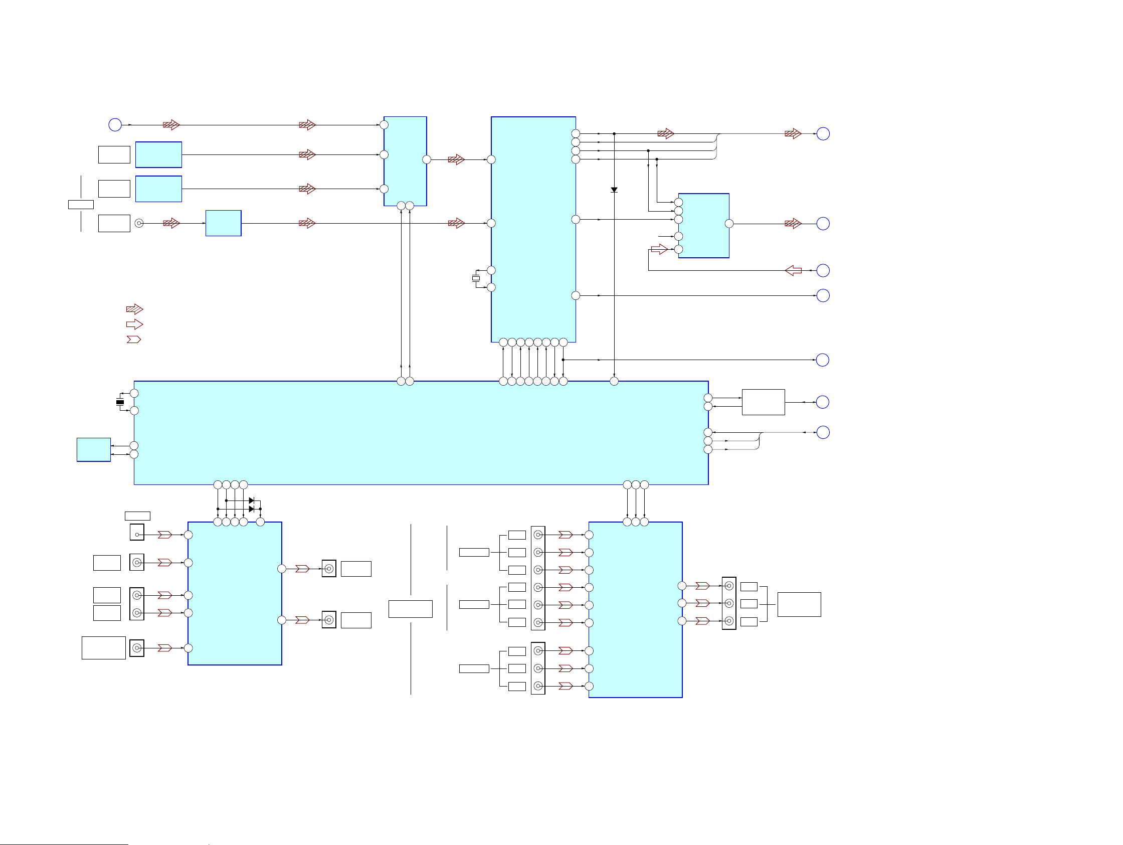
STR-KG800
1515
SECTION 6
DIAGRAMS
EEPROM
IC1131
SYSTEM CONTROLLER
IC1010 (1/4)
DIGITAL OPTICAL
RECEIVER
IC1352
DIR_DO
DIR_DI
DIR_CLK
DIR_CE(LAT)
DIR ERROR
DIR_XMODE (RESET)
DIR_XSTATE
DIR DATA0
63
DATA0, BCK
LRCK, CKOUT
DOUT
7
SCKI
12
BCK
8
LRCK
13
VINL
14
VINR
6
XMCK
20
DATAO
16
BCK
14
LRCK
15
CKOUT
13
AUDIO
24
46
TV OPT
IN
DIGITAL OPTICAL
RECEIVER
IC1351
OPT SAT
IN
SCHMITT
TRIGGER
IC1303
DIGITAL AUDIO
INTERFACE RECEIVER
IC1301
DIN2
J1301
5
COAX IN
DVD
DIGITAL
A/D CONVERTER
IC1401
21
22
X1301
12.288MHz
XOUT
XIN
DIRCKST
39
D1301
57
58
X1
X0
98
EEPROM DATA
78
EEPROM CLK
X1101
12.5MHz
A
• SIGNAL PATH
: AUDIO (ANALOG)
: AUDIO (DIGITAL)
• R-ch is omitted due to same as L-ch.
DATA SELECTOR
IC1302
1C2
5
1C3
3
1C1
6
DIN0
3
1Y
7
2
B
CKSEL0
DOUTDICLKCEXMODE
XSTATE
ERROR
14
A
TC74HC153_A
36
TC74HC135_B
35
CEC DATA
SWITCH
Q1103 – 1106
HDMI_TX
HDMI_RX
HDMI RESET
104
103
103
29
CEC OUT
CEC IN
88
AUDIO
A_AUDIO
D_AUDIO
B
N
M
ERR
C
CEC
D
48 47 45 46 492938
RESET, TX, RX
E
J
SPDIF
R-CH
35 36 38 37 48 17 34
VIDEO 1 IN
VIDEO 1
VIDEO IN
VIDEO 2 IN/
PORTABLE A V IN
VIDEO
DVD
VIDEO IN
SAT
VIDEO IN
DMPORT_VIDEO
17
J1302 (1/2)
J210 (1/2)
J211 (1/2)
J298 (1/2)
DMPORT
VIDEO 1
VIDEO OUT
MONITOR
VIDEO OUT
J210 (2/2)
J220 (1/2)
J221
J211 (2/2)
VIDEO AMP
IC210
VIN3
7
VIN1
13
VIN5
3
VIN4
5
VIN2
9
VOUT1
1
VOUT2
15
SW114SW210SW34SW46SW5
2
34
V_SW133V_SW232V_SW331V_SW4
D211
D210
: VIDEO
COMPONENT
VIDEO
VIDEO AMP
IC220
CH1 IN1
1
CH2 IN1
8
CH3 IN1
17
CH1 IN2
3
CH2 IN2
14
CH3 IN2
15
CH1 IN3
5
CH2 IN3
12
CH3 IN3
13
SW12SW2
4PS23
35
COMP_S136COMP_S237PS(V-MUTE)
PB/CB
Y
P
R/CR
DVD IN
P
B/CB
Y
P
R/CR
SAT IN
P
B/CB
Y
P
R/CR
J220 (2/2)
CH1 OUT
24
CH2 OUT
22
CH3 OUT
20
P
B/CB
Y
P
R/CR
COMPONENT
VIDEO
MONITOR OUT
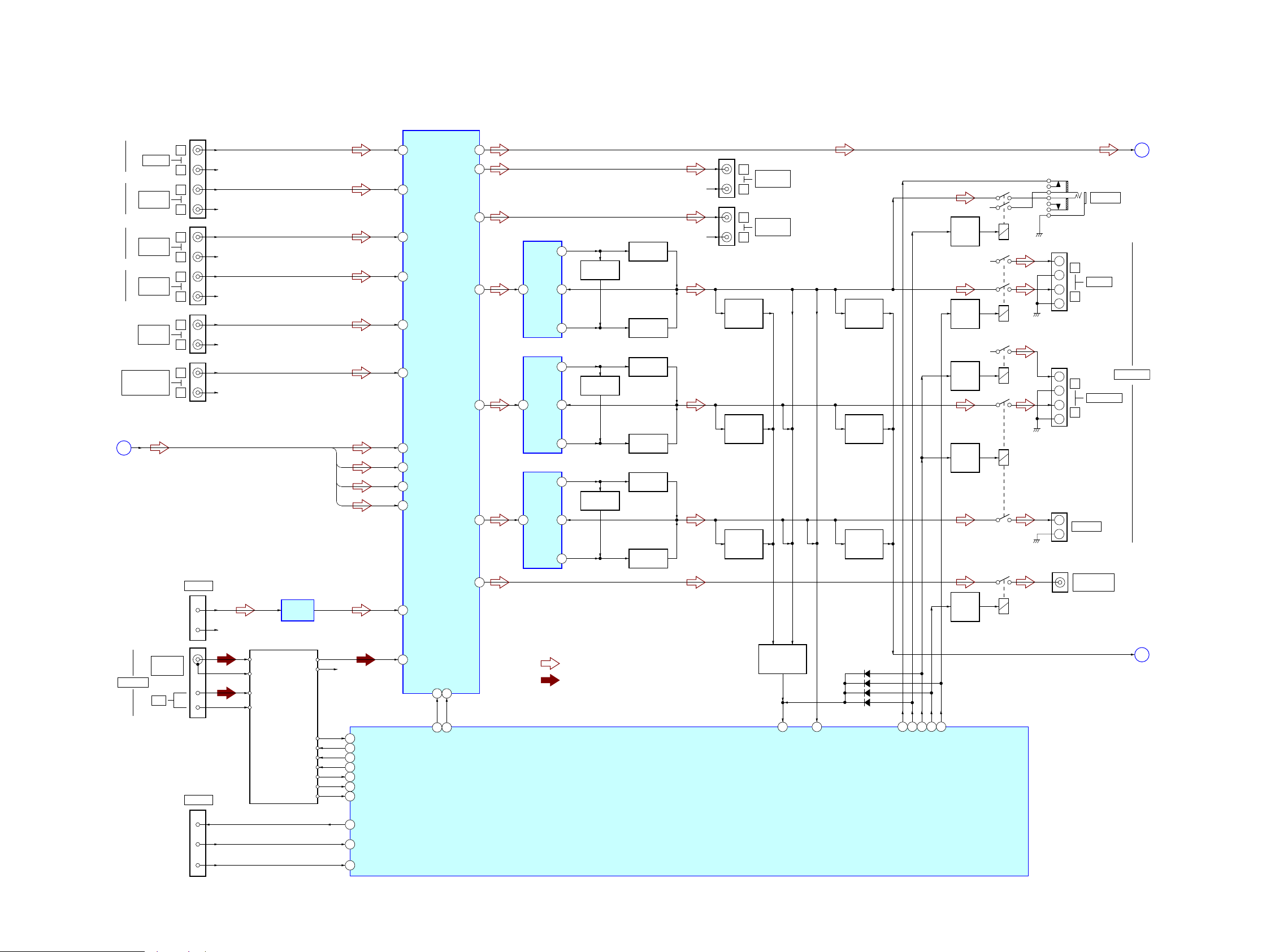
6-1. BLOCK DIAGRAM - MAIN Section -
(Page 16)
(Page 17)
(Page 17)
(Page 18)
(Page 17)
(Page 17)
(Page 16)
(Page 16)
STR-KG800
STR-KG800
1616
• SIGNAL PATH
: AUDIO (DIGITAL)
: VIDEO
HDMI CONTROLLER
IC3519
CN3501
HDMI
SAT IN
A32
52
B32
51
7
9
A33
55
B33
54
4
6
A34
58
B34
57
1
3
A31
49
B31
48
10
DATA0+
DATA0–
DATA1+
DATA1–
DATA2+
DATA2–
CLOCK+
CLOCK–
SDA (5V)
SCL (5V)
+5V POWER
HOT PLUG DET
18
CEC
13
12
16
15
HDMI
INPUT
SELECTOR
IC3503
55
P5V_SELA
56
P5V_SELB
SDA3
45
19
HPD3
44
SCL3
46
CN3502
HDMI
DVD IN
A22
71
B22
70
7
9
A23
74
B23
73
4
6
A24
77
B24
76
1
3
A21
68
B21
67
10
DATA0+
DATA0–
DATA1+
DATA1–
DATA2+
DATA2–
CLOCK+
CLOCK–
SDA (5V)
SCL (5V)
+5V POWER
HOT PLUG DET
18
CEC
13
12
16
15
SDA2
63
19
HPD2
62
SCL2
64
CN3503
HDMI
VIDEO 2/
BD IN
A12
9
B12
8
7
9
A13
12
B13
11
4
6
A14
15
B14
14
1
3
A11
6
B11
5
10
DATA0+
DATA0–
DATA1+
DATA1–
DATA2+
DATA2–
CLOCK+
CLOCK–
SDA (5V)
SCL (5V)
+5V POWER
HOT PLUG DET
18
CEC
13
12
16
15
SDA1
2
19
HPD1
80
SCL1
3
RX_HPD1
HDMI RECEIVER
IC3511
HDMI
TRANSCEIVER
IC3513
Y1
34
Z1
35
51
50
Y2
31
Z2
32
55
54
Y3
28
Z3
29
59
58
Y4
25
Z4
26
63
RXC+
RXC–
RX0+
RX0–
RX1+
RX1–
RX2+
RX2–
DSDA
DSCL
62
41
PWR5V
44
42
CSDA
CSCL
39
40
SCL_SINK
38
HPD_SINK
40
xOE
42
SDA_SINK
39
S1
21
S2
22
S3
23
LEVEL
SHIFT
IC3501
(1/2)
LEVEL SHIFT
IC3507
S [1]
S [2]
S [3]
SIGNAL SELECTOR
IC3504
2Y2
2
2Y3
4
2Y1
5
3
2-COM
10
9
A
B
21
51 52 53
S [1]
S [2]
S [3]
TMDS_S1
TMDS_S2
TMDS_S3
DATA SELECTOR
IC3521
EEPROM
IC3509
2Y1
5
2Y0
1
1Y1
14
1Y0
12
3
2-COM
13
1-COM
5
SDA
6
SCL
EEPROM1
10
A
7
WP
35
TMDS_OEB
54
RX_RST
19
MUTE
65
RX_INT
20
TX_INT
43
TX_RST
42
CSCL
27
CSDA
28
124 – 121,117 – 114,
111 – 108, 105 – 99,
96 – 92
QE0 – QE23
79 – 75, 70 – 67
65 – 61, 58 – 49
D0 – D23
ODCK
119
HSYNC
128
VSYNC
1
DE
127
SPDIF
70
SD0 – SD3
4
24
MCK
79
SCK
76
WS
75
MUTE
67
RESET
89
INT
91
IDCK
66
HSYNC
1
VSYNC
2
DE
80
74 – 71
SPDIF
5
SD0 – SD3
MCK
6
SCK
12
WS
11
10 – 7
TX0+
30
TX0–
29
7
9
TX1+
33
TX1–
32
4
6
TX2+
36
TX2–
35
1
3
TXC+
27
TXC–
26
10
HPD
DATA0+
DATA0–
DATA1+
DATA1–
DATA2+
DATA2–
CLOCK+
CLOCK–
SDA (5V)
SCL (5V)
HOT PLUG DET
CEC
18 19
12
16
15
13
DSDA
19
DSCL
20
INT
17
RESET
42
CSDA
44
CSCL
43
LEVEL
SHIFT
IC3501 (2/2)
LEVEL
SHIFT
Q3504
CN3504
HDMI
OUT
SPDIF
LRCK
MCK
BCK
SD0 – SD3
85
84
XTALIN
XTALOUT
X3501
28.322MHz
10RESET
RESET, TX, RX
D
13
11
XIN
XOUT
X3502
10MHz
B+ SWITCH
Q3505-3507
F
G
E
33TX
34RX
CEC
MUTE
SD0-3, MCK,
BCK, LRCK
J
41TX_5VPWR
K
5VPWR
6-2. BLOCK DIAGRAM - HDMI Section -
(Page 15)
(Page 17)
(Page 15)
(Page 17)
(Page 15)
(Page 19)
STR-KG800
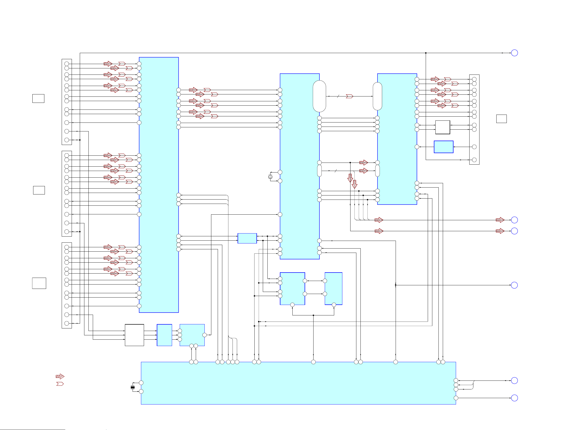
STR-KG800
1717
A
M
DATA0, BCK, LRCK, CKOUT
G
MUTE
LRCK
DATA0
SD1
INPUT SELECTOR
IC1008
2
A0
3B0
CKOUT
5A1
6B1
SD0
BCK
SD2
SD3
11 A2
LRCK
BCK
10 B2
MCK
13 B3
Y0
4
Y1
7
Y2
9
S
1
Y3
12
14 A3
• SIGNAL PATH
D_AUDIO
F
DATA SELECTOR
IC1017
1A
2B
Y
5
A/B
6
C
HDMI_ERR
30
DSP_SELECT
22
SYSTEM CONTROLLER
IC1010 (2/4)
D FLIP-FLOP
IC1014
78 DPSIA
79 DPSIB
88 DPLRCK
INVERTER
IC1016
HDMI_RSRATE
50
94 DPFSCK
89 DPBCK
16 FLAG1
82 DPSIE
81 DPSID
80 DPSIC
DSP SPDIF(LAT)
65
DSP RESET
64
DSPINT
81
XSPIDS
XRESET
FLAG0
DSP
IC1009
D/A CONVERTER
IC1452
2MCK
3BCK
4 LRCK
9 DIN3
7 DIN1
8 DIN2
10 DIN4
VO1L
21
VO1R
22
VO2L 23
VO2R
24
VO3L 25
VO3R 26
DPDVLRCK
64
DPDVBCK
DPSOA
DPSOB
DPSOC
DPSOD
87
65
66
67
86
DSP SPICLK
: AUDIO (ANALOG)
: AUDIO (DIGITAL)
143
142
X1302
25MHz
XTAL
CLKIN
SD0-3, MCK, BCK, LRCK
97 XNONAUDIO
B
AUDIO
ERR
115
DCAC_IN
122
121
15
75
DSP MOSI
74
DSP MISO
73
SPICLK
MOSI
MISO
125
121 126
DAC_ATC
26
DCAC_DSP_IN
82
DAC_DI
4
DACMUTE
27
DAC CLK
1
11
13
14
M/I2S
MD/DM
MUTE
12
MC/IWL
LINE AMP
IC1404
LINE AMP
IC1405
LINE AMP
IC1406
R-CH
R-CH
SL
L, C, SW, SL
C
L
SW
R
• R-ch is omitted due to same as L-ch.
AUTO
CAL MIC
J2000
MIC AMP
IC2000
RESET SIGNAL
BUFFER
IC1005
62RESET_TRG
55INIT
RESET SIGNAL
GENERATOR
IC1007
RESET
SWITCH
IC1006
STBY +3.3V
D1504
6-3. BLOCK DIAGRAM - DSP Section -
(Page 15)
(Page 15)
(Page 16)
(Page 15)
(Page 15)
(Page 16)
(Page 18)
STR-KG800
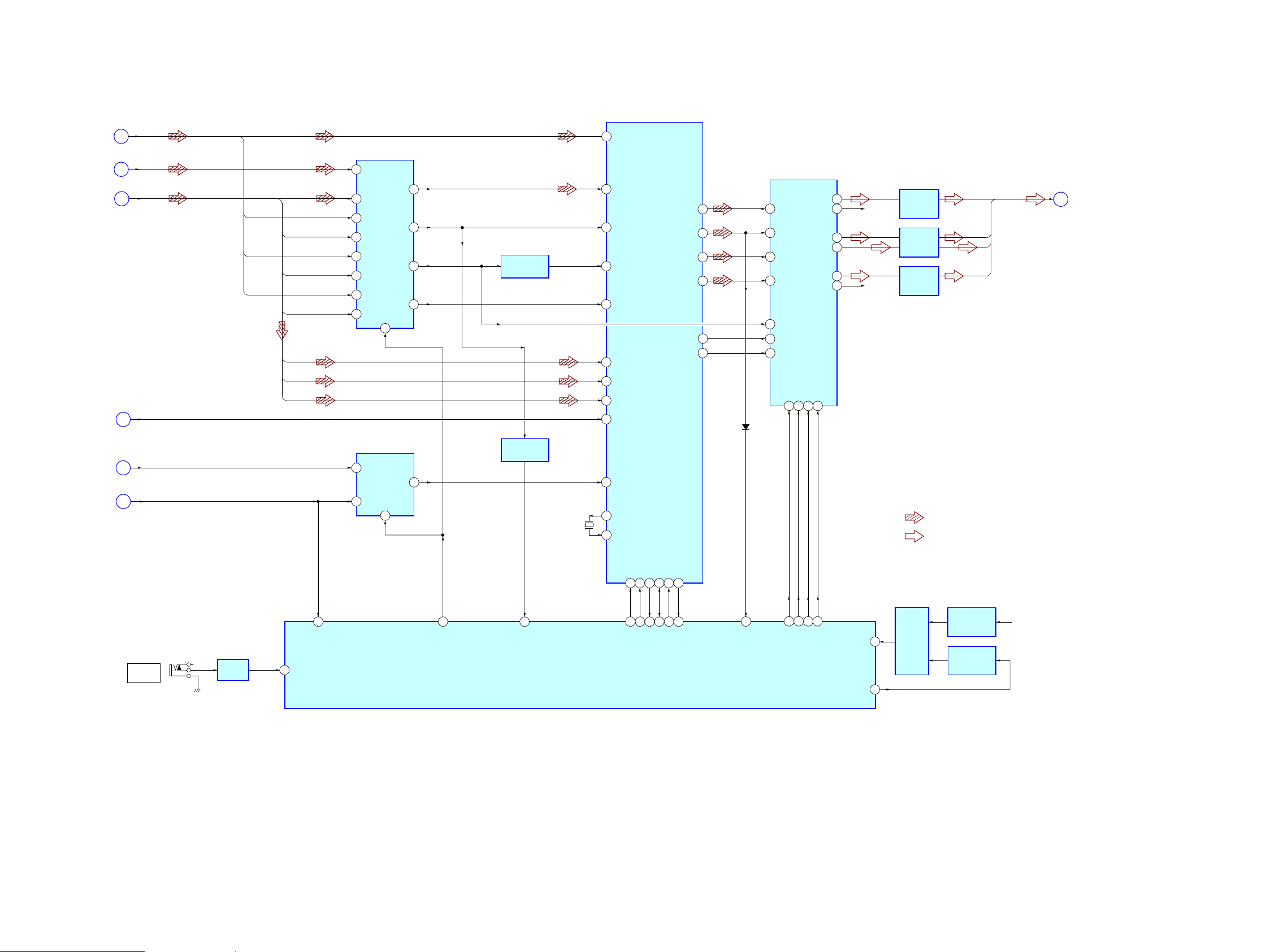
STR-KG800
1818
SYSTEM CONTROLLER
IC1010 (3/4)
10
DATA11CLK
L CH
R CH
DO
DI
INL1 (TUNER_L)
63
VOL_CLK
10
VOL_DA
11
27
LOUT
76
RECL1
29
FM 75Ω
COAXIAL
72
69
26
DVD
AUDIO IN
ANTENNA
TUNER (FM/AM)
AM
INL2 (DMPORT_L)
61
L+
R+
14
13
CN1302 (2/3)
R-CH
CLINK_RX
CLINK_TX
6
5
CN1302 (3/3)
INPUT SELECTOR,
ELECTRICAL VOLUME
IC400
R-CH
FM ANT
GND
AM ANT
GND
CLOCK
CE
TUN_DO
TUNER DATA
TUNER CLK
TUN_LAT
INL9
47
INL7
51
TV IN
J401 (1/2)
SA-CD/CD
CD-R IN
L
R
L
R
R-CH
R-CH
INL12
41
INL11
43
J403
SAT
AUDIO IN
L
R
L
R
R-CH
R-CH
VIDEO 2 IN/
PORTABLE A V IN
AUDIO
INL5
55
SLIN
68
CIN
70
SWIN
71
LIN
72
J298 (2/2)
L
R R-CH
BUFFER
IC3002
117
SD TUNE SD
100
CLINK_RX
99
CLINK_TX
DET
7
101
C_LINK_DET
87
RDS DATA
RDS DATA
RDS INT RDS INT
• SIGNAL PATH
: TUNER
: AUDIO (ANALOG)
• R-ch is omitted due to same as L-ch.
A_AUDIO
N
DMPORT
DMPORT
VIDEO 1
AUDIO IN
INL13
38
J404 (1/2)
L
R R-CH
FLOUT
14
P_DET
Q
SL
L, C, SW, SL
C
L
SW
R
J401 (2/2)
L
R
SA-CD/CD
CD-R OUT
R-CH
RECL2
27
J404 (2/2)
L
R
VIDEO 1
AUDIO OUT
R-CH
+VOUT1
2
NF1
5
-VOUT1
3
LIMITER
Q701, 702
BOOSTER
Q703
BOOSTER
Q704
CURRENT
DETECT
Q711, 712
IN1
6
POWER AMP
IC700
AF POWER
PROTECT
Q720
RELAY
DRIVE
Q350
RELAY
DRIVE
Q375
PROTECTOR
68
16 17
VACS_CTRL
119
PROTECT
SWITCH
Q320, 321, 325
SLOUT
18
+VOUT1
2
NF1
5
-VOUT1
3
LIMITER
Q801, 802
BOOSTER
Q803
BOOSTER
Q804
CURRENT
DETECT
Q811, 812
IN1
6
POWER AMP
IC800
AF POWER
PROTECT
Q820
COUT
16
+VOUT2
12
NF2
9
-VOUT2
11
LIMITER
Q651, 652
BOOSTER
Q653
BOOSTER
Q654
CURRENT
DETECT
Q661, 662
IN2
8
POWER AMP
IC600
AF POWER
PROTECT
Q670
SWOUT
15
+
−
+
−
RELAY
DRIVE
Q301
RY301
RY355
RY360
RY350
RY375
RELAY
DRIVE
Q360
R-CH
R-CH
+
−
+
−
R-CH
RELAY
DRIVE
Q355
+
−
HP_DETECT
HP_RY
SW RY
C/SUR/SB
12 13
FRONT A RY
14
D1112
D1111
D1108
D1107
J790
PHONES
TB601
L
R
FRONT
TB604
L
R
SURROUND
SPEAKERS
TB607
CENTER
J405
SUB WOOFER
AUDIO OUT
86
6-4. BLOCK DIAGRAM - AUDIO Section -
(Page 15)
(Page 19)
(Page 17)
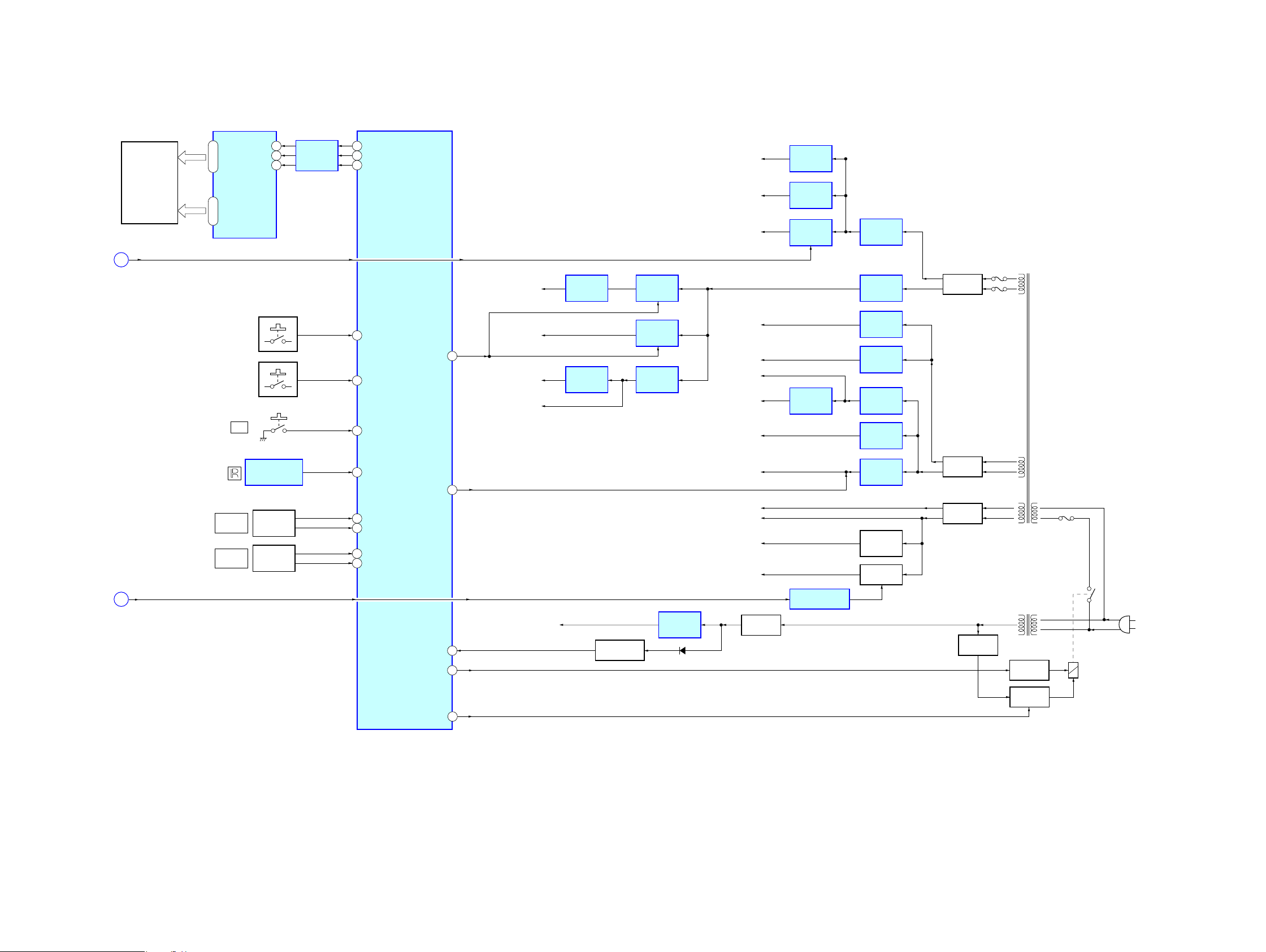
STR-KG800
STR-KG800
1919
(AC IN)
F901
B+
B-
POWER AMP -45V
FL -20V
TU +9V
VIDEO +5V
DSP +3.3V
DSP +1.2V
HDMI +3.3V
HDMI +1.8V
HDMI +5V
FL +5V
DMPORT +5V
VIDEO -5V
A-7V
A+5V
A+7V
SYS +3.3V
9
POWER_RY
25FUSE_DETECT
7
HDMI_REG_CTL
SYSTEM CONTROLLER
IC1010 (4/4)
71
FL_DATA
70
FL_CLK
69
FL LAT
FLUORESCENT
INDICATOR TUBE DRIVER
IC100
7
DIN
8
CLK
9
STB
FLUORESCENT
INDICATOR
TUBE
FL101
SEG1 – SEG16,
SEG17
14 – 29, 31
GRID1 – GRID11
42 – 32
84
SIRCS_IN
ROTARY
ENCODER
RV101
LEVEL SHIFT
IC101
REMOTE CONTROL
RECEIVER
IC103
INPUT
SELECTOR
I/
S109 – 112, 115
85
POWER KEY
113
AD_KEY1
S101 – 108
114
AD_KEY2
90
89
INPUT ENCODER A
S100
INPUT ENCODER B
ROTARY
ENCODER
RV102
MASTER
VOLUME
80
79
VOL_JOG (2B)
VOL_JOG (2A)
Q
83STOP
P_DET
K
5VPWR
SUB POWER
TRANSFORMER
T904
RELAY DRIVE
Q901
RECT
D950 – 953
RECT
D910 – 913
RECT
D921
#%1((&'6'%6
Q990
RY901
D990, 991
+3.3V
REGULATOR
IC1904
+5V
REGULATOR
IC201
+9V
REGULATOR
IC1902
+4.1V
REGULATOR
IC4100
+3.3V
REGULATOR
IC3527
+1.8V
REGULATOR
IC3528
+1.2V
REGULATOR
IC1002
+3.3V
REGULATOR
IC3526
+3.3V
REGULATOR
IC1013
+6.3V
REGULATOR
IC4001
+7V
REGULATOR
IC350
-20V
REGULATOR
Q930
B- SWITCH
Q500, 501
+5V
REGULATOR
IC1001
+5V
REGULATOR
IC3516
+5V
REGULATOR
IC1031
+5V
REGULATOR
IC1012
MAIN POWER
TRANSFORMER
T901
PROTECT DETECT
IC565
RECT
D4001, 4002
-5V
REGULATOR
IC202
-7V
REGULATOR
IC352
F4002
F4001
97SUBT
RECT
D955
B+ SWITCH
Q951, 955
6-5. BLOCK DIAGRAM - POWER SUPPLY Section -
(Page 16)
(Page 18)
STR-KG800
STR-KG800
2020
For Schematic Diagrams.
Note:
• All capacitors are in μF unless otherwise noted. (p: pF)
50 WV or less are not indicated except for electrolytics
and tantalums.
• All resistors are in Ω and 1/4 W or less unless otherwise
specifi ed.
• f : internal component.
• 2 : nonfl ammable resistor.
• 5 : fl usible resistor.
• C : panel designation.
THIS NOTE IS COMMON FOR PRINTED WIRING BOARDS AND SCHEMATIC DIAGRAMS.
(In addition to this, the necessary note is printed in each block.)
• A : B+ Line.
• B : B– Line.
• Voltages and waveforms are dc with respect to ground
under no-signal (detuned) conditions.
no mark : TUNER
• V oltages are taken with a VOM (Input impedance 10 MΩ).
Voltage variations may be noted due to normal production
tolerances.
• Waveforms are taken with a oscilloscope.
V oltage variations may be noted due to normal production
tolerances.
• Circled numbers refer to waveforms.
• Signal path.
J : AUDIO (DIGITAL)
F : AUDIO (ANALOG)
f : TUNER
E : VIDEO
For Printed Wiring Boards.
Note:
• X : Parts extracted from the component side.
• Y : Parts extracted from the conductor side.
• f : Internal component.
• : Pattern from the side which enables seeing.
(The other layers' patterns are not indicated.)
• Indication of transistor.
CEB
These are omitted.
Caution:
Parts face side:
(SIDE A)
Pattern face side:
(SIDE B)
Parts on the parts face side seen from
the pattern face are indicated.
Parts on the pattern face side seen from
the parts face are indicated.
• Circuit Boards Location
Caution:
Pattern face side:
(Conductor Side)
Pattern face side:
(Component Side)
Parts on the pattern face side seen from
the pattern face are indicated.
Parts on the parts face side seen from
the parts face are indicated.
Note: The components identifi ed by mark 0 or dotted
line with mark 0 are critical for safety.
Replace only with part number specifi ed.
C
Q
B
E
These are omitted.
POWER board
DCAC board
HEADPHONE board
VIDEO 2 board
STANDBY board
DISPLAY board
DCDC CONVERTER board
HDMI board
TUNER (FM/AM)
DIGITAL AB board
MAIN board
VIDEO board
STR-KG800
STR-KG800
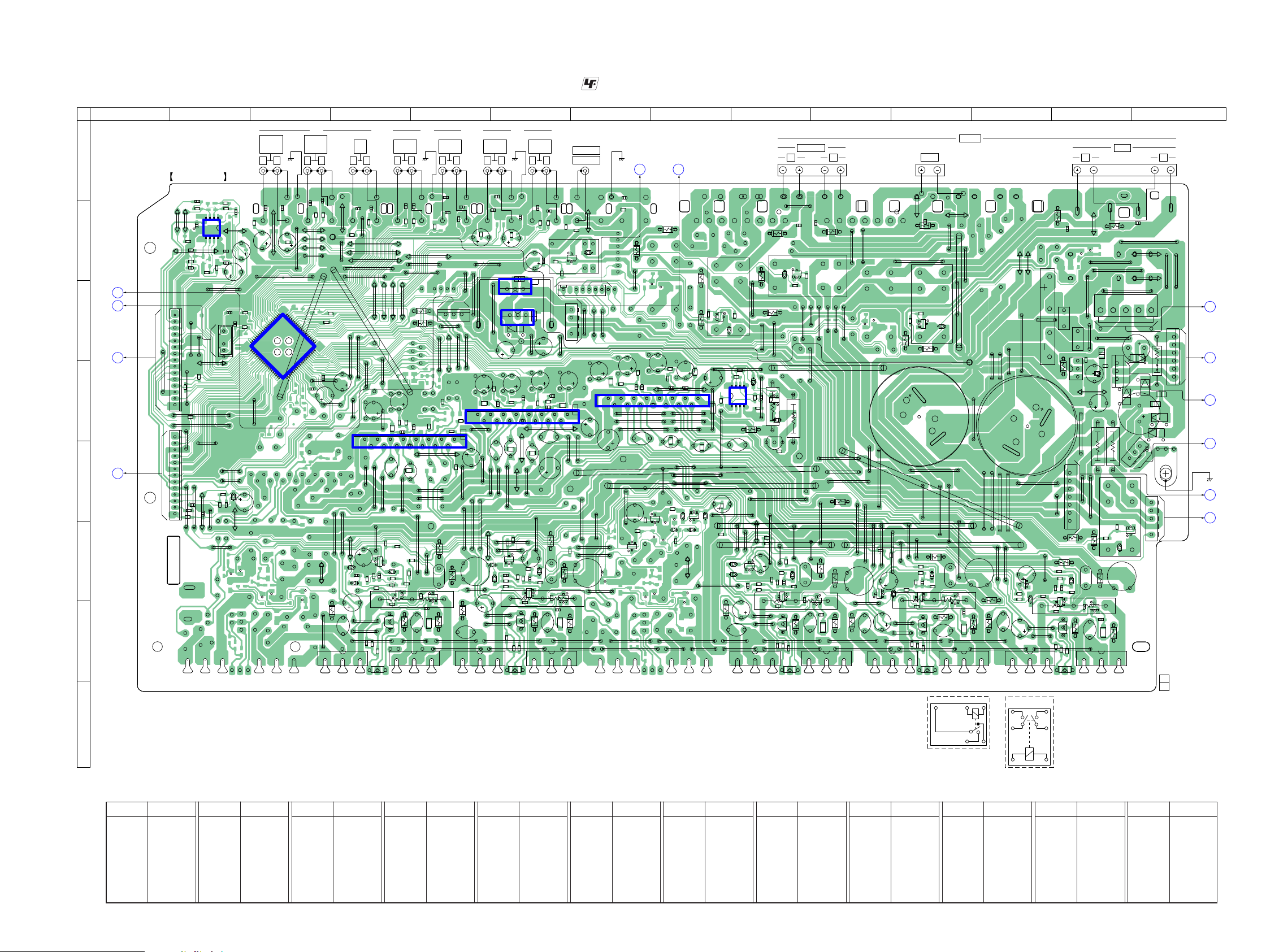
2121
E
20
21
41
60
40
61
80
1
E
E
E
D940
R401
D941
R402
D942
R403
D943
R404
R405
R408
R409
R600
Q661
Q662
R602
R605
D375
D761
Q861
R801
Q862
R802
R803
Q670
R804
R805
R806
R807
R808
D770
Q870
D775
R811
R814
R815
R816
R430
R431
R820
R821
R822
R823
R824
C400
C403
C405
R830
R449
R450
R451
R452
R453
R454
R455
C802
R458
C804
R459
R651
R652
R653
R654
R656
R657
R658
C811
R466
R467
R851
R852
R853
C430
R854
C431
R661
R856
R857
R470
R664
R858
R665
R666
C820
R861
R670
R864
R671
R865
R672
R866
R673
R674
R675
R676
C449
R870
R871
R872
R873
C450
R680
R874
Q301
R880
C652
C654
Q501
C852
C854
C661
JR406
Q320
JR605
C861
Q321
JR606
JR607
C670
Q325
C675
Q711
Q712
C870
D811
C489
Q720
D820
C499
JR434
JR435
Q350
Q355
Q360
R301
R304
R501
R502
R503
R504
R505
R506
R507
D661
Q375
Q761
R701
Q762
R702
R703
R704
R705
R706
R707
R320
R708
D861
D670
R325
R326
R327
Q770
R328
D675
R711
R714
R715
R716
D870
R335
R336
R337
R720
R721
R722
R723
R724
R725
R726
CL001
CL003
R730
C500
R350
R353
R930
R931
R355
C702
R358
C704
R360
C900
R363
C711
R751
R752
R753
R754
R756
R757
R758
C720
R375
R378
R761
C725
R764
R765
R766
R770
R771
R772
R773
R774
C350
R775
R776
C352
C933
R780
CC01
D301
CC02
CC03
CC04
C940
CC05
C941
CC08
CC09
C752
C754
D500
D501
E
E
CC11
CC12
CC15
CC16
CC17
C761
D320
JR702
D325
D326
D327
C770
JR320
JR321
D711
JR322
C775
Q811
C3022
Q812
C3025
C3026
C3027
D335
D720
Q820
D725
C3032
C3037
R3010
R3011
R3012
R3013
5
8
1
4
JR340
D350
CC51
CC52
D352
CC53
CC54
R3020
D930
CC55
R3021
D355
D931
R3022
R3023
CC58
CC59
D360
5
8
1
4
E
E
E
E
E
E
E
E
E
E
E
E
E
E
E
E
E
E
EB
2
15
1
6
EB
2
14
1
15
2
14
1
15
1
13
1
15
EB
143
173
E
B
153
2
14
1
15
1
3
EB
BECBECBECBE
C
BECBECBECBECBECBE
C
3
213
3
1
1
3
1
3
1
7
1
E
B
E
BEB
EB EBE
B
E
B
Q654
JW758
TB601
CNP912
JW760
Q851
JW761
Q852
JW762
Q853 Q854
HS350
IC350
IC352
JW766
JW767
JW768
JW769
CNP921
JW770
JW771
JW772
JW773
JW776
JW777
R809
JW779
CNP930
R810
JW781
R812
JW782
R813
JW783
JS710
JS711
JW785
JS712
JW789
CNP940
L678
JW790
JS335
JW791
JS336
JS337
JS338
JW794
JS339
JW795
R828
JW798
R829
JW799
L878
C408
C409
JS920
JS922
JWH1
JWH2
JWH3
JWH4
JWH5
JWH7
JWH9
C801
C803
JS930
C805
C806
C807
C808
C809
R659
R660
R662
R663
JS3001
R859
JS3002
C821
R860
R862
R863
C829
R678
R679
R487
JS578
R488
JS388
C644
JS389
R878
R879
JS3022
JS778
C458
C459
JS392
JS393
JS394
C844
C651
C653
JW600
C655
JW601
C656
JW602
C657
JW603
C658
JW604
Q500
C659
JW605JW606
JW607
JW608
C851
JW609
JS3037
C853
JW800
C855
JW801
C856
JW802
C857
JW803
C858
JW610
JW804
C471
C859
Q701
JW611
Q702
JW612
Q703
JW613
JW807
Q704
JW614
JW615JW616
JW617
JW618
JW619
C671
JW813
JW620
JW814
JW621
JW815
JW622
JW816
JW623
JW817
C679
JW819
JW626
C487
JW627
C488
C871
JW629
RR11
RR12
IC600
RR15
TB604
TB607
RR16
RR17
JW630
C879
JW631
JW825
JW632
JW826
JW633
JW827
JW634
JW635
JW829
JW636
JW637
IC800
JW638
JW639
JW830
JW831
JW832
JW833
JW640
JW834
JW641
JW835
JW642
JW836
JW643
JW837
JW644
CNP410
JW838
JW645
CNP411
JW839
JW646
JW647
JW648
L728
Q930
JW840
JW841
JW842
JW843
JW650
JW651
JW845
JW652
JW846
JW653
JW655
JW656
JW657
JW658
JW659
R302
R303
JW852
JW660
Q751
JW661
JW855
Q752
Q753
CNP430
Q754
JW664
JW859
JW665
JW667
JS400
JS401
JS402
JW860
JW861
JW862
JW863
JS408
JW864
JW670
JS409
JW671
JW866
JW672
JW867
JW868
R510
R511
JW675
JW676
JW677
JS410
JS411
R709
JW679
JWH10
JW870
JWH11
JW871
JWH12
JW872
R710
CN500
JW681
R712
R713
JW684
JS611
JW685
JW686
JW687
JW688
JW689
JS810
JW690
JW691
JW692
JW693
JW694
JW695
JW696
R728
R729
JW699
JS432
JS628
L778
R545
R351
R546
R352
C701
R356
R932
C703
R357
C705
C706
C707
C320
C708
C709
R361
C325
R362
C904
R940
JS458
JS459
CN350
JS460
JS461
R759
C335
C721
R376
R377
R760
R762
R763
C729
RY301
JS470
C920
CN941
JS471
C921
JS472
C922
JS473
C923
C351
C545
C546
C353
R778
C930
R779
C931
R392
C932
R393
C744
C751
C753
JW700
C755
C756
C757
C758
JW704
C759
JW705
JW706
JW707
JW708
JW321
JW709
JW322
JW323
JW324
JW325
JW326
JW327
JW328
JW710
JW329
Q801
Q802
JW712
Q803
JW713
Q804
JW714
JW715
JW716
JW717
JW330
JW718
JW331
JW332
C771
CN792
JW720
JW721
C3024
RY350
C779
RY355
IC700
W001
ET902
W002
JW731
RY360
C3034
CNP500
JW737
JW738
D921
JW739
JW740
JW741
JW743
JW745
JW746
JW747
JW748
RY375
JW749
L828
JW750
JW751
JW752
JW753JW754
Q651
JW755
Q652
JW756
Q653
J401 J403 J404
J405
IC3002
IC565
IC400
MAIN BOARD
1-875-588-
H
DCAC
BOARD
CN2000
C
VIDEO 2
BOARD
CNP201
B
A
DIGITAL
AB
BOARD
CNS502
DIGITAL
AB
BOARD
CNS501
J
MAIN POWER
TRANSFORMER
T901
MAIN POWER
TRANSFORMER
T901
L
DIGITAL
AB
BOARD
CNP505
K
STANDBY BOARD
CN912
E
HEADPHONE
BOARD
CNP790
M
DISPLAY
BOARD
CN108
N
G
VIDEO
BOARD
CNP203
F
DIGITAL
AB BOARD
CNP504
LR
TV
IN
LR
SA-CD/CD/
CD-R
IN
LR
SA-CD/CD/
CD-R
OUT
LR
SAT
AUDIO IN
LR
DVD
AUDIO IN
LR
VIDEO 1
AUDIO OUT
LR
VIDEO 1
AUDIO IN
SUB WOOFER
AUDIO OUT
CENTER
SURROUND
RL
FRONT
SPEAKERS
LR
RY350, 355
RY360, 375
-1
-2
RY301
12
(12)
(CHASSIS)
(CHASSIS) (CHASSIS) (CHASSIS) (CHASSIS)
A
B
C
D
E
F
G
H
1 2 3 4 5 6 7 8 9 10 11 12 13 14
6-6. PRINTED WIRING BOARD - MAIN Board -
• : Uses unleaded solder.
• See page 20 for Circuit Boards Location.
Ref. No. Location
• Semiconductor Location
Ref. No. Location Ref. No. Location Ref. No. Location Ref. No. Location Ref. No. Location Ref. No. Location Ref. No. Location Ref. No. Location Ref. No. Location Ref. No. Location Ref. No. Location
D301 B-7
D320 F-8
D325 F-8
D326 E-8
D327 E-8
D335 E-2
D350 C-11
D352 C-6
D355 B-9
D360 C-8
D375 F-13
D500 D-9
D501 D-9
D661 F-4
D670 F-4
D675 F-4
D711 F-9
D720 F-9
D725 F-9
D761 F-6
D770 F-6
D775 F-6
D811 F-12
D820 F-13
D861 F-11
D870 F-11
D921 C-12
D930 C-14
D931 D-13
D940 D-14
D941 D-14
D942 D-13
D943 D-14
IC350 C-6
IC352 C-6
IC400 C-3
IC565 D-9
IC600 E-4
IC700 D-6
IC800 D-7
IC3002 B-2
Q301 B-7
Q320 E-8
Q321 F-7
Q325 E-8
Q350 C-11
Q355 B-9
Q360 C-8
Q375 F-13
Q500 E-9
Q501 D-9
Q651 G-4
Q652 G-4
Q653 G-4
Q654 G-5
Q661 F-5
Q662 F-4
Q670 F-4
Q701 G-9
Q702 G-9
Q703 G-9
Q704 G-10
Q711 F-10
Q712 F-9
Q720 F-9
Q751 G-6
Q752 G-6
Q753 G-5
Q754 G-6
Q761 F-6
Q762 F-6
Q770 F-6
Q801 G-13
Q802 G-13
Q803 G-12
Q804 G-13
Q811 G-13
Q812 G-13
Q820 F-12
Q851 G-11
Q852 G-11
Q853 G-11
Q854 G-11
Q861 F-11
Q862 F-11
Q870 F-10
Q930 D-13
(Page 32)
(Page 38)
(Page 31)
(Page 31)
(Page 31) (Page 38)
(Page 44)
(Page 44)
(Page 40)
(Page 32)
(Page
44)
(Page
31)
STR-KG800
STR-KG800
2222
BOARD
MAIN
(2/3)
1
BOARD
MAIN
(2/3)
4
2
BOARD
(3/3)
MAIN
3
(3/3)
BOARD
MAIN
IC B/DIC B/DIC B/D
2.8
1.1
-1.1
-43.2
0.1
0.1
0.1
0.1
-43.2
-1.1
1.1
44.8
-44.8
1.1
0.1
1.1
0.1
-43.2
0.1
2.8
0.1
44.8
-44.8
-43.2
-1.1
-1.1
1.1
0
0
0.1
-43.1
0.1
2.8
0
44.8
-44.8
-44.8
0
-1.1
0
0
0
0
-0.6
-1.1
0.5
1.1 -1.1
0.5
1.1
-0.6
-1.1
-1.1
0.5
1.1
-0.6
-1.1
-1.1
1.1
0.5
-1.1
-1.1
-0.6
1.1
0.5
-1.1
-1.1
-0.6
-44.8
0
-1.1
44.8
0
1.1
-44.8
-1.1
0
1.1
0
44.8
-44.8
-1.1
0
1.1
0
44.8
-44.8
-1.1
0
1.1
0
44.8
-44.8
-1.1
0
1.1
0
44.8
0
-43.8-43.8
0
0
-43.8
0
0
-43.8
0
0
-43.8
0
0
0
0
0
0
0
0
0
0
0
0
0
0
0
4.14.1
0
4.1
0
4.1
0
4.1
0
560
R658
15kR672
500V
C658
47p
123
MN2488-OPY-MK
Q653
BCE
6.2k
R662
47kR680
2.2k
R656
100kR676
2SA1163L-TE85L
Q662
1.5kR664
2SA1115TP-EF
Q651
50V
10
C671
0.022
C679
82k
R657
4.7kR661
2SA1163L-TE85L
Q661
68kR666
2SC3052EF-T1-LEF
Q670
25V
47
C657
10
R679
123
MP1620-OPY-MK
Q654
BCE
L678
15kR665
0.22
R663
0.01
C670
220p
C661
2SC3623ATP-LK
Q652
500V
47p
C659
4.7
R678
2SA1163L-TE85L
Q711
560
R808
0.22
R813
123
MN2488-OPY-MK
Q803
BCE
47k
R830
0.22
R863
500V
C758
47p
2SA1163L-TE85L
Q862
2SA1115TP-EF
Q701
123
MN2488-OPY-MK
Q753
BCE
25V47C807
4.7kR811
47k
R780
82k
R857
2SA1115TP-EF
Q801
100k
R776
68kR854
2SA1163L-TE85L
Q762
1.5kR764
2SC3623ATP-LK
Q702
4.7kR861
1.5k
R714
100p
C804
500V
C708
47p
0.01C870
560
R708
50V
10
C771
123
MP1620-OPY-MK
Q804
BCE
220p
C711
4.7k
R761
500V3p
C805
25V
47
C857
68kR766
2SC3052EF-T1-LEF
Q770
68kR704
1.5k
R814
R805
22k
25V
47
C757
123
MN2488-OPY-MK
Q703
BCE
10
R779
10
R729
L878
15kR815
500V3p
C855
123
MP1620-OPY-MK
Q754
BCE
15kR822
2SA1163L-TE85L
Q712
2.2k
R706
500V
C858
47p
2SC3052EF-T1-LEF
Q720
0.01C720
1.5kR864
R705
22k
100p
C704
220p
C761
2SC3623ATP-LK
Q752
100p
C754
4.7
R778
560
R758
500V
47p
C709
0.01C820
15kR772
2SA1163L-TE85L
Q811
2SC3623ATP-LK
Q802
68kR754
100p
C854
2.2k
R856
0.022
C879
500V
47p
C809
2SA1163L-TE85L
Q812
2.2k
R756
68kR804
50V10C721
L828
123
MP1620-OPY-MK
Q854
BCE
220p
C861
500V
3p
C705
25V47C707
68kR816
2SA1115TP-EF
Q851
2SA111 5TP-EF
Q751
50V10C821
10
R879
82k
R707
L728
2.2k
R806
15kR722
4.7kR711
10
R829
500V
C808
47p
0.022
C779
2SA1163L-TE85L
Q861
82k
R757
560
R858
4.7
R728
0.022
C729
2SA1163L-TE85L
Q761
123
MP1620-OPY-MK
Q704
BCE
6.2kR862
500V
47p
C859
15kR865
2SC3052EF-T1-LEF
Q870
15kR872
68kR866
47k
R880
15kR715
L778
4.7
R878
6.2kR812
15kR765
2SC3623ATP-LK
Q852
0.22
R763
0.01
C770
0.22
R713
0.01
C775
6.2k
R712
82k
R807
500V3p
C755
50V10C871
123
MN2488-OPY-MK
Q853
BCE
0.022
C829
68kR716
4.7
R828
220p
C811
500V
47p
C759
2SC3052EF-T1-LEF
Q820
115 14 13 12 11 10
uPC2581V-S
IC700
115 14 13 12 11 10
uPC2581V- S
IC800
100V
10
C546
1
R546
1
R545
100V
10
C545
500V
3p
C655
100p
C654
50V
C651
10
R605
22k
1k
R651
100p
C652
68kR654
68k
R652
1k
R751
1kR701
50V
C751
10
100p
C752
100p
C702
50V
C701
10
68k
R752
68k
R702
1k
R851
1k
R801
50V
C851
10
100p
C852
100p
C802
50V
C801
10
68k
R852
68k
R802
R730
47k
MA2J1110GLS0D661
MA2J1110GLS0
D675
MA2J1110GLS0D870
MA2J1110GLS0D820
MA2J1110GLS0D861
MA2J1110GLS0
D670
MA2J1110GLS0D811
MA2J1110GLS0D761
MA2J1110GLS0
D770
MA2J1110GLS0D720
MA2J1110GLS0
D775
MA2J1110GLS0D711
MA2J1110GLS0
D725
100k
R726
0.01
C725
0JR605
0JR606
22kR720
22kR670
22kR870
22kR770
22kR820
50V
C644
10
50V
C844
10
50V
C744
10
JR607
0
JS628
3.3kR771
3.3kR821
3.3kR871
22kR824
22kR674
22kR724
22kR874
22kR774
22kR773
22k
R873
22kR723
22kR673
22kR823
100
R760
100
R859
100
R709
100
R809
100
R810
100
R860
100
R710
100
R660
100
R659
100
R759
2.2kR853
2.2k
R703
2.2k
R803
2.2kR753
2.2kR653
JS712
JS710
JS611
JS810
JS711
6.2k
R762
JS337
JS339
JS338
0
R600
0
R602
500V
33p
C853
500V
33p
C803
500V
33p
C653
500V
33p
C703
500V
33p
C753
10V
C706
220
10V
C756
220
10V
C856
220
10V
C656
220
10V
C806
220
JR340 0
JS578
3.3kR671
3.3kR721
10k
R675
10k
R725
10k
R775
0.01
C675
15 14 13 12 11 10 9 8 7 6 5 4 3 2 1
uPC2581V-S
IC600
MUTE
+VOUT1
-VOUT1
COMP1
NF1
IN1
GND
IN2
NF2
COMP2
-VOUT2
+VOUT2
VCC
VCC
VEE
MUTE
+VOUT1
-VOUT1
COMP1
NF1
IN1
GND
IN2
NF2
COMP2
-VOUT2
+VOUT2
VCC
VCC
VEE
MUTE
+VOUT1
-VOUT1
COMP1
NF1
IN1
GND
IN2
NF2
COMP2
-VOUT2
+VOUT2
VCC
VCC
VEE
98765432 98765432
13
15
17
18
19
20
21
22
23
242
1
3
11
12
4
6
9
10
25
26
27
(1/3)MAIN BOARD
POWER AMP
IC800
POWER AMP
IC700
POWER AMP
IC600
BOOSTERBOOSTERBOOSTER BOOSTERBOOSTER BOOSTERBOOSTER BOOSTERBOOSTER BOOSTER
Q651, 652
LIMITER
Q751, 752
LIMITER
Q701, 702
LIMITER
Q851, 852
LIMITER
Q801, 802
LIMITER
Q811, 812
CURRENT
DETECT
AF POWER
PROTECT
DETECT
CURRENT
Q861, 862
DETECT
CURRENT
Q711, 712
DETECT
CURRENT
Q761, 762
DETECT
CURRENT
Q661, 662
PROTECT
AF POWER
PROTECT
AF POWER
PROTECT
AF POWER
PROTECT
AF POWER
D
B
1610 11
F
5 15
L
K
3
G
1 12
C
E
H
8967
J
4 13
A
142
I
6-7. SCHEMATIC DIAGRAM - MAIN Board (1/3) -
• See page 46 for IC Block Diagrams.
(Page
23)
(Page
24)
(Page 24)
(Page
23)
STR-KG800
STR-KG800
2323
(2/5)
DIGITAL
AB BOARD
CNS502
A
C
VIDEO 2
CNP201
BOARD
(1/3)
BOARD
MAIN
4
MAIN
BOARD
(3/3)
5
BOARD
MAIN
6
(3/3)
BOARD
MAIN
7
(3/3)
BOARD
(3/3)
8
MAIN
MAIN
BOARD
(1/3)
1
B
CNS501
(2/5)
AB BOARD
DIGITAL
IC B/D
7
0
0
0
0
0
0
-6.9
0
0
-6.9
0
0
0
0
0
0
7
0
0
0
0
0
0
0
0
0
0
0
0
0
0
0
0
0
0
0
0
0
0
0
0
0
0
0
0
0
0
0
0
0
R3010
47k
R3011
47k
C3037
1
C3032
1
C3027
1
R3012
47k
R3013
47k
R3021 47k
R3022
47k
50V
C3024
4.7
50V
C3034
4.7
C3025
0.1
C3022
1
R3020 47k
C3026
0.1
8765
1234
NJM4565M(TE2)
IC3002
CC02
100p
CC52
100p
50V
C409
4.7
R451
1k
50V
C459
4.7
R402
1k
R459
1k
R409
1k
CC01
100p
CC51
100p
CC09
100p
R401
1k
R452
1k
J401
6P
CC59
100p
R453
1k
CC03
100p
CC53
100p
R403
1k
R454
1k
CC04
100p
CC54
100p
R404
1k
C403
2200p
R405
1k
50V
C458
4.7
R455
1k
R408
1k
CC05
100p
CC08
100p
50V
C408
4.7
CC58
100p
CC55
100p
R458
1k
C405
2200p
6.8k
R335
0.1
C489
100p
C449
0.1
C499
100p
C450
JR434
0
JR435
0
C430 220p
C431
220p
MAZ8030G0LS0
D335
1
2
3
4
5
6
7
8
9
10
11
12
13
14
15
16
17
18
19
20
21
22
23
24
25
26
27
28
29
30
31
32
33
34
35
36
37
38
39
4041
42
43
44
45
46
47
48
49
50
51
52
53
54
55
56
57
58
59
60
61
62
63
64
65
66
67
68
69
70
71
72
73
74
75
76
77
78
79
80
BD3471KS2
IC400
INPUT SELECTOR,
ELECTRICAL VOLUME
GND
HPFN
LPF01
LPF02
LPFN2
LPFN1
SWVOL
VCC
DGND
DATA
CLK
VEE
FROUT
FLOUT
SWOUT
COUT
SROUT
SLOUT
SBROUT
SBLOUT
GND
GND
RECL4
RECR4
RECL3
RECR3
RECL2
RECR2
RECL1
RECR1
GND
INL16
INR16
INL15
INR15
INL14
INR1
INL1
INR13
GND
INL12
INR12
INL11
INR11
INL10
INR10
INL9
INR9
INL8
INR8
INL7
INR7
INL6
INR6
INL5
INR5
INL4
INR4
INL3 (DCAC_MIC)
INR3 (DCAC_MIC)
INL2 (DMPORT_L)
INR2 (DMPORT_R)
INL1 (TUNER_L)
INR1 (TUNER_R)
GND
SBLIN
SBRIN
SLIN
SRIN
CIN
SWIN
LIN
RIN
GND
ROUT
LOUT
GND
ROUT SUB
LOUT SUB
GND
1
2
3
4
5
6
7
8
9
10
11
12
13
13P
CNP410
VOL IC CLK
VOL IC DATA
VACS CTRL
PROTECTOR
+7V
-7V
FR OUT
AGND
FL OUT
SW
AGND
C OUT
SR OUT
1
2
3
4
5
6
7
8
9
10
11
12
13
14
15
15P
CNP411
AGND
SL OUT
+7V
SBR OUT
SBL OUT
L IN
AGND
R IN
TUNER R
AGND
TUNER L
DMPORT LDMPORT RDMPORT L+
DMPORT R+
R3023
47k
1
3
4
CNP430
4P
L-CH
2
NC
GND
R-CH
R430
1k
R431
1k
JS335
JS409
JS410 JS411
JS461
JS459
JS460
JS400
1kR449
1k
R450
JS408
JS458
JS3002
JS3037
JS3022
JS3001
JS336
J403
4P
J404
4P
JS401
JS432
R487
2.2
R488
2.2
25V
C487
47
25V
C488
47
0
R336
22k
R337
16V
47
C335
28
29
30
31
32
964121110
3
1
2
MAIN BOARD (2/3)
BUFFER
IC3002
IC400
ANALOG SOUND PROCESSOR
W001-002
VEE
VCC
(CHASSIS) (CHASSIS) (CHASSIS)
LR
CD-R OUT
SA-CD/CD/
LR
SA-CD/CD/
CD-R IN
LR
TV IN
LR
SAT AUDIO
IN
LR
DVD AUDIO
IN
LR
VIDEO 1
AUDIO OUT
LR
VIDEO 1
AUDIO IN
D
B
10 11
F
5
K
3
G
1 12
C
E
H
8967
J
4 13
A
142
I
6-8. SCHEMATIC DIAGRAM - MAIN Board (2/3) -
• See page 46 for IC Block Diagrams.
(Page 22)
(Page 26)
(Page 26)
(Page 39)
(Page 22)
(Page 24)
(Page 24)
(Page 24)
(Page 24)
STR-KG800
STR-KG800
2424
8
TRANSFORMER
T901
MAIN POWER
J
STANDBY
CN912
K
BOARD
CNP505
DIGITAL
(4/5)
L
AB BOARD
DISPLAY
CN108
M
BOARD
BOARD
(2/3)
MAIN
N
MAIN POWER
T901
TRANSFORMER
E
CNP790
BOARD
HEADPHONE
2
(1/3)
BOARD
MAIN
BOARD
(2/3)
MAIN
5
MAIN
(1/3)
BOARD
3
MAIN
(2/3)
BOARD
6
CNP504
F
(4/5)
AB BOARD
DIGITAL
BOARD
G
VIDEO
CNP203
CN2000
BOARD
DCAC
H
BOARD
(2/3)
7
MAIN
167
-16.8-6.9
-19.8
-20.4
-44.8
0.8
0.20.2
0.8
0.2
0.8
6.4
-43.8
-5.5
6.4
3.3
0
0
16
-44.8
-44.8
3.2
0
-44.3
-44.8
-44.8
0.1
0.7
-5.5
-5.
7
5
-3.6
-5.5
1.2
-6.9
C400
2200p
R466
1k
R470
47k
RY301
2SC3052EF-T1-LEF
Q301
50V
C471
4.7
R467
100k
100V
0.22
C920
100V
0.22
C921
39k
R326
50V
10
C325
10k
R327
6.8k
R325
2SC3052EF-T1-LEF
Q325
2SA1163L-TE85L
Q320
2SC3052EF-T1-LEF
Q321
1k
R328
10k
R503
220k
R507
2SC1815GR-TPE2
Q500
10k
R504
8765
4321
NJM4565M(TE2)
IC565
470k
R502
10k
R505
0.1
C500
2SB734-T-34
Q930
100V
0.1
C933
35V
47
C931
4.7
R932
22k
R930
PTZ-TE25-5.6B
D930
10k
R931
35V
47
C932
1SR154-400TE-25
D352
0.47
C350
0.47
C352
1SR154-400TE-25
D943
0.47
C940
16V
3300
C904
0.47
C941
1SR154-400TE-25
D941
1SR154-400TE-25
D940
1SR154-400TE-25
D942
E
ET902
1
2
4
4P
CN500
+15V
NC
3
GND
-15V
2.2k
R375
2SC3052EF-T1-LEF
Q375
RY375
1
3
4
5
5P
CN792
HP_DETECT
2
NC
R-CH
GND
L-CH
2SC3052EF-T1-LEF
Q360
RY360
12V
2SC3052EF-T1-LEF
Q355
RY355
12V
RY350
12V
2SC3052EF-T1-LEF
Q350
2.2k
R350
RT1P241C-TP- 1
Q501
1k
R355
1k
R360
R301
2.2k
MA2J1110GLS0
D360
MA2J1110GLS0
D326
MA2J1110GLS0
D501
MA2J1110GLS0
D350
MA2J1110GLS0
D325
MA2J1110GLS0
D355
MA2J1110GLS0
D375
MA2J1110GLS0
D320
MA2J1110GLS0
D327
MA2J1110GLS0
D301
JS922
JS920
1
2
3
4
5
6
6P
CNP940
F1
NC
GND
F2
R4 -AC
R4 +AC
10
RR11
0.01
CC11
0.01
CC12
10
RR12
0.01CC15
10
RR15
0.01CC16
10
RR16
10
RR17
0.01
CC17
1
3
5
5P
CNP921
R1 (UPPER TAP)
2
NC
4
NC
R1 GND
R1 (UPPER TAP)
1
2
3
3P
CNP500
+7V
GND
-7V
MAZ8200GMLS0
D931
47
R362
33
R361
47
R357
33
R356
47
R352
33
R351
47
R37733R376
R302
100
R303
100
D5SBA20-4003
D921
~
~
C923
6800
71V
C922
6800
71V
0
JR320
2W680
R393
2W
R392
680
1
3
4
5
6
7
7P
CN350
HP RY
2
NC
SW PREOUT RY
FRONT A RY
2W
R510
330
MAZ8220GMLS0
D500
22k
R501
33k
R506
JS470 JS471
JS472
JS473
JS393
JS394
JS392
JR406
0
2W
100
R511
G
TA7807S
IC350
1
2
3
IIO
O
G
TA79007SB
IC352
1
2
3
47k
R358
47k
R363
47k
R353
47k
R304
47kR378
1
2
3
3P
CNP930
-20V
F1
F2
JS388
JS389
J405
1
2
3
4
5
6
7
7P
CNP912
R2 RETURN GND
NC
-15V
STBY GND
R2 GND IN
+15V
+15V (NC)
1
2
3
3P
CN941
GND (R4)
+7V (R4)
GND (R4) (NC)
JS930
35V
47
C930
10V
220
C320
100k
R320
C900
0.1
1/2W
0.15
R940
16V
100
C353
16V
100
C351
21
23
24
18
13
22
15
20
19
17
25
26
27
28
29
30
31
32
MAIN BOARD (3/3)
PROTECT DETECT
IC565
+7V REGULATOR
IC350
-7V REGULATOR
IC352
(CHASSIS)
AUDIO OUT
SUB WOOFER
B- SWITCH
B- SWITCH
LIMITER
PROTECT SWITCH
PROTECT SWITCH
RELAY DRIVE
VCC
VEE
RELAY DRIVE
RELAY DRIVE
RELAY DRIVE
-2
-1
-2
-1
-2
-1
-1
-2
(CHASSIS)
-20V REGULATOR
W001-002
+
+
-
R
L
L
R
CENTER
+
-
TB607
SURROUND
TB604
+
-
R
FRONT
-
L
+
R
L
TB601
SPEAKERS
RELAY DRIVE
D
B
1610 11
F
5 153
G
1 12
C
E
H
8967
J
4 13
A
142
I
HP_DETECT
C/SUR/SB_RY
FRONT B RY (NC)
6-9. SCHEMATIC DIAGRAM - MAIN Board (3/3) -
(Page 33)
(Page 22)
(Page 23)
(Page 22)
(Page 23)
(Page 28)
(Page 39)
(Page 33)
(Page 23)
(Page 45)
(Page 45)
(Page 28)
(Page 41)
(Page 23)
(Page 45)
 Loading...