

Sony STR-K995 Service Manual
STR-K995
Q
Q
3
7
6
3
1
5
1
5
0
SERVICE MANUAL
Ver. 1.0 2007.05
TEL 13942296513 QQ 376315150 892498299
• STR-K995 is the tuner and the amplifier section
in HT-DDW995.
This receiver incorporates Dolby* Digital and Pro Logic Surround and
the DTS** Digital Surround System.
* Manufactured under license from Dolby Laboratories.
“Dolby”, “Pro Logic” and the double-D symbol are trademarks of
Dolby Laboratories.
** “DTS” and “DTS Digital Surround” are registered trademarks of
DTS, Inc.
SPECIFICATIONS
8
9
2
4
9
2
8
US Model
9
9
TEL 13942296513 QQ 376315150 892498299
TEL
13942296513
AUDIO POWER
SPECIFICATIONS
POWER OUTPUT AND TOTAL
HARMONIC DISTORTION:
With 6 ohm loads, b oth ch annels drive n, from
120 – 20,000 Hz; rated 90 watts per channel
minimum RMS power, with no more than 1%
total harmonic distortion from 250 milliwatts
to rated outpu t.
Amplifier section
Power Output
Models of area code US
Stereo mode (rated) (6 ohms 1 kHz
Surround mode (reference) (6 ohms 1 kHz
THD 10%)
1)
90 W + 90 W
RMS output
FRONT: 140 W
per channel
CENTER: 140 W
SURROUND: 140 W
per channel
, THD 1%)
2)
1)
Measured under the following conditions:
Area code Power requirements
US 120 V AC, 60 Hz
2)
Reference power outpu t for fro nt , c ent e r and
surround speakers. Depending on the sound field
settings and the source, there ma y be no sound
output.
Inputs
Analog Sensitivity: 800 mV/
Digital (Coaxial) Impedance: 75 oh m s
Outputs (Analog)
,
AUDIO OUT Voltage: 800 mV/
SUBWOOFER Voltage: 2 V/1 kohm
Tone
Gain levels ±6 dB, 1 dB step
Reproduction frequency range:
Q
Q
50 kohms
10 kohms
28 – 20,000 Hz
3
7
6
3
1
FM tuner section
0
5
1
5
Tuning range 87.5 - 108.0 MHz
Antenna FM wire antenna
Antenna terminals 75 ohms, unbalanced
Intermedia te frequency
AM tuner section
Tuning range
With 10-kHz tuning scale:
With 9-kHz tuning scale:
Antenna Loop antenna
Intermedia te frequency
3)
You can change the AM tuning scale to 9 kH z or
10 kHz. After tuning in any AM station, turn off
the receiver. While holding down TUNING
MODE, press ?/1. All preset stations will be
erased when you change the tu ning scal e. To reset
the scale to 10 kHz (or 9 kHz), repea t the
procedure.
8
9
9
4
2
10.7 MHz
530 – 1,710 kHz
531 – 1,710 kHz
450 kHz
— Continued on next page —
8
2
9
9
3)
3)
w
w
9-887-679-01
2007E16-1
© 2007.05
w
.
xia
Sony Corporation
Home Audio Division
Published by Sony Techno Create Corporation
o
y
u
1
6
MULTI CHANNEL AV RECEIVER
3
.
c
o
m
STR-K995
r
7
Video section
Q
Q
Inputs/Outputs
Video: 1 Vp-p, 75 ohms
COMPONENT VIDEO:
General
Power requirements
Area code Power requirements
US 120 V AC, 60 Hz
TEL 13942296513 QQ 376315150 892498299
Power output (DIGITAL MEDIA PORT)
DC OUT: 5 V, 700 mA
Power consumption
Area code Power consumption
US 200 W
Power consumption (during stand by mode)
Dimensions (width/height/depth) (Approx.)
Mass (Approx.) 7.8 kg (17 lb 4 oz)
3
Y: 1 Vp-p, 75 ohms
P
75 ohms
P
75 ohms
80 MHz HD Pass Through
0.3 W
430 × 157.5 × 310 mm
(17 × 6 1/4 × 12 1/4 inches)
including projec t i ng parts
and controls
B/CB
: 0.7 Vp-p,
R/CR
: 0.7 Vp-p,
6
3
1
5
1
5
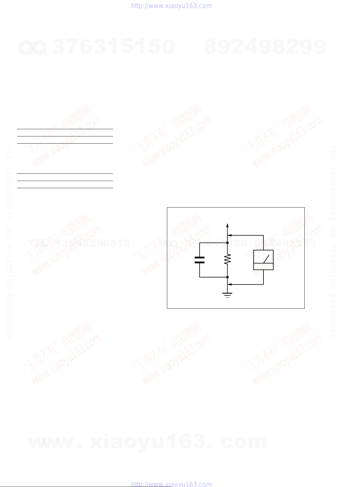
SAFETY CHECK-OUT
0
After correcting the original service problem, perform the following
safety check before releasing the set to the customer:
Check the antenna terminals, metal trim, “metallized” knobs, screws,
and all other exposed metal parts for AC leakage.
Check leakage as described below.
LEAKAGE TEST
The AC leakage from any exposed metal part to earth ground and
from all exposed metal parts to any exposed metal part having a
return to chassis, must not exceed 0.5 mA (500 microamperes.).
Leakage current can be measured by any one of three methods.
1. A commercial leakage tester, such as the Simpson 229 or RCA
WT -540A. Follow the manuf acturers’ instructions to use these
instruments.
2. A battery-operated AC milliammeter . The Data Precision 245
digital multimeter is suitable for this job.
3. Measuring the voltage drop across a resistor by means of a
VOM or battery-operated AC voltmeter . The “limit” indication
is 0.75 V, so analog meters must hav e an accurate low-voltage
scale. The Simpson 250 and Sanwa SH-63Trd are examples
of a passive VOM that is suitable. Nearly all battery operated
digital multimeters that have a 2 V A C range are suitable. (See
Fig. A)
2
9
8
To Exposed Metal
Parts on Set
4
9
8
2
9
9
TEL 13942296513 QQ 376315150 892498299
TEL
Design and specifications are subject to
change without notice.
13942296513
8
9
4
2
9
8
0
5
1
5
1
3
6
7
3
Q
Q
AC
1.5 k
0.15 µF
Fig. A. Using an AC voltmeter to check AC leakage.
SAFETY-RELATED COMPONENT WARNING!!
COMPONENTS IDENTIFIED BY MARK 0 OR DOTTED LINE
WITH MARK 0 ON THE SCHEMATIC DIAGRAMS AND IN
THE PARTS LIST ARE CRITICAL TO SAFE OPERATION.
REPLACE THESE COMPONENTS WITH SONY PARTS WHOSE
PART NUMBERS APPEAR AS SHOWN IN THIS MANUAL OR
IN SUPPLEMENTS PUBLISHED BY SONY.
Ω
Earth Ground
voltmete
(0.75 V)
2
9
9
2
w
w
w
.
xia
o
y
u
1
6
3
.
c
o
m

E
STR-K995
Q
TEL 13942296513 QQ 376315150 892498299
Notes on chip component replacement
Q
• Never reuse a disconnected chip component.
• Notice that the minus side of a tantalum capacitor may be
UNLEADED SOLDER
Boards requiring use of unleaded solder are printed with the leadfree mark (LF) indicating the solder contains no lead.
(Caution: Some printed circuit boards may not come printed with
Unleaded solder has the following characteristics.
• Unleaded solder melts at a temperature about 40 °C higher
• Strong viscosity
• Usable with ordinary solder
About area codes
TEL
Th
e area code of the receiver you purchased is
shown on the lower right portion of the rear panel
(see the illustration below).
BACK PANEL
LL
NT ARSURROUND
RS
Any differences in operation , according to the area
code, are clearly indicated in the text, for example,
“Models of area code AA only”.
Moreover, it is possible to distinguish the model
by Part No..
Model Part No.
US Model 2-897-800-9
7
3
damaged by heat.
the lead free mark due to their particular size)
: LEAD FREE MARK
than ordinary solder.
Ordinary soldering irons can be used but the iron tip has to be
applied to the solder joint for a slightly longer time.
Soldering irons using a temperature regulator should be set to
about 350 °C.
Caution: The printed pattern (copper foil) may peel away if
Unleaded solder is more viscou-s (sticky, less prone to flow)
than ordinary solder so use caution not to let solder bridges
occur such as on IC pins, etc.
It is best to use only unleaded solder but unleaded solder may
also be added to ordinary solder.
6
the heated tip is applied for too long, so be careful!
13942296513
R
CENTER
3
Part No.
1
Area code
5
1
5
0
Q
Q
1. GENERAL ................................................................... 4
2. TEST MODE ............................................................... 11
3. ELECTRICAL ADJUSTMENT ............................. 13
4. DIAGRAMS................................................................. 14
4-1. Block Diagram – MAIN Section –.................................. 15
4-2. Block Diagram – DISPLAY/POWER Section –............. 16
4-3. Block Diagram – HDMI Section –.................................. 17
4-4. Printed Wiring Board – DIGITAL Board (Side A) –...... 18
4-5. Printed Wiring Board – DIGITAL Board (Side B) –...... 19
4-6. Schematic Diagram – DIGITAL Board (1/5) – .............. 20
4-7. Schematic Diagram – DIGITAL Board (2/5) – .............. 21
4-8. Schematic Diagram – DIGITAL Board (3/5) – .............. 22
4-9. Schematic Diagram – DIGITAL Board (4/5) – .............. 23
4-10. Schematic Diagram – DIGITAL Board (5/5) – .............. 24
4-11. Printed Wiring Board – MAIN Board – ......................... 25
4-12. Schematic Diagram – MAIN Board (1/4) – ................... 26
4-13. Schematic Diagram – MAIN Board (2/4) – ................... 27
4-14. Schematic Diagram – MAIN Board (3/4) – ................... 28
4-15. Schematic Diagram – MAIN Board (4/4) – ................... 29
4-16. Printed Wiring Boards
4-17. Schematic Diagram
4-18. Printed Wiring Boards
4-19. Schematic Diagram
7
3
4-20. Printed Wiring Boards
4-21. Schematic Diagram
4-22. Printed Wiring Boards
4-23. Schematic Diagram
4-24. Printed Wiring Board – HDMI RE Board – ................... 38
4-25. Schematic Diagram – HDMI RE Board (1/2) – ............. 39
4-26. Schematic Diagram – HDMI RE Board (2/2) – ............. 40
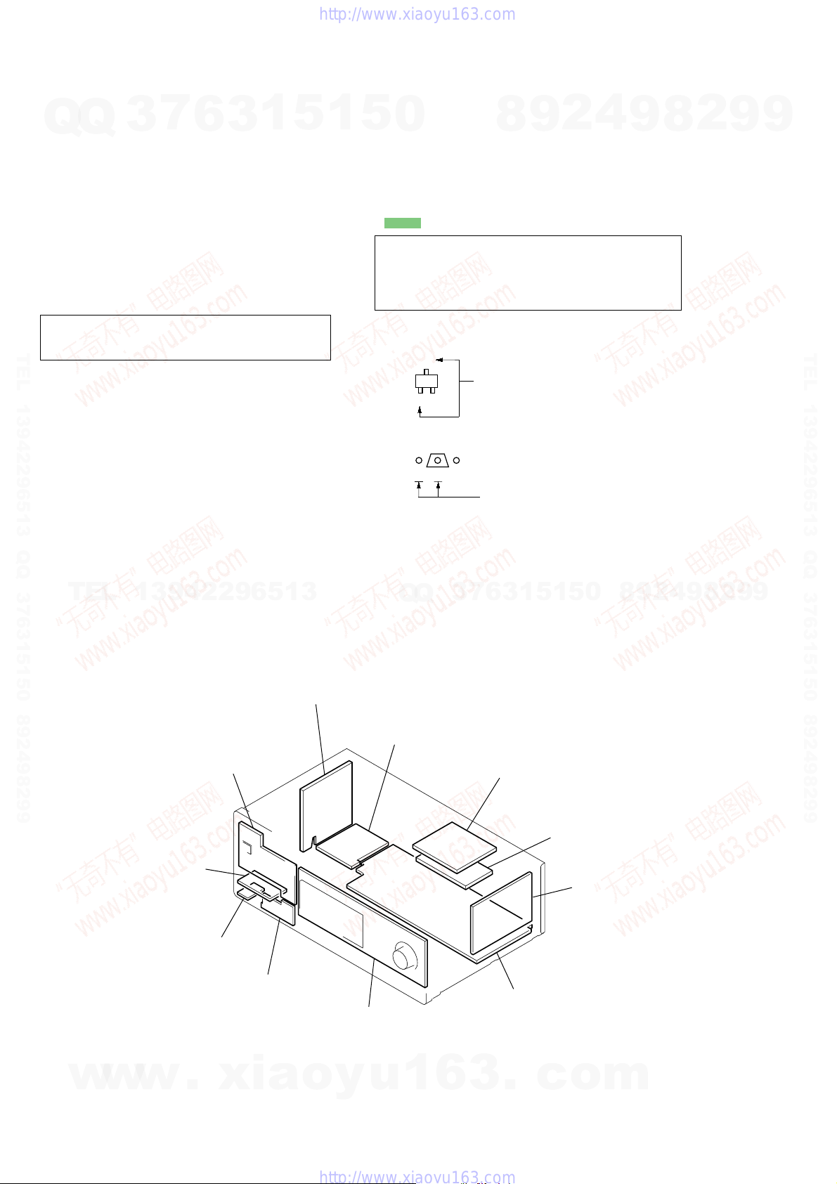
5. EXPLODED VIEWS
5-1. Front Panel Section ......................................................... 56
5-2. Chassis Section................................................................ 57
6. ELECTRICAL PARTS LIST .................................. 58
4
8
– DISPLAY Board, POWER KEY Board – .................... 30
– DISPLAY Board, POWER KEY Board – .................... 31
– STANDBY Board, DCDC Board – .............................. 32
3
6
– STANDBY Board, DCDC Board – .............................. 33
– DCAC Board, VIDEO3 Board – .................................. 34
– DCAC Board, VIDEO3 Board – .................................. 35
– VIDEO Board, HEADPHONE Board –....................... 36
– VIDEO Board, HEADPHONE Board –....................... 37
TABLE OF CONTENTS
0
5
1
5
1
2
9
9
8
9
2
8
4
2
9
8
9
2
9
9
9
TEL 13942296513 QQ 376315150 892498299
w
w
w
.
xia
o
y
u
1
6
3
.
c
o
m
3
STR-K995
SECTION 1
GENERAL
This section is extracted
from instruction manual.
7
Q
Q
TEL 13942296513 QQ 376315150 892498299
3
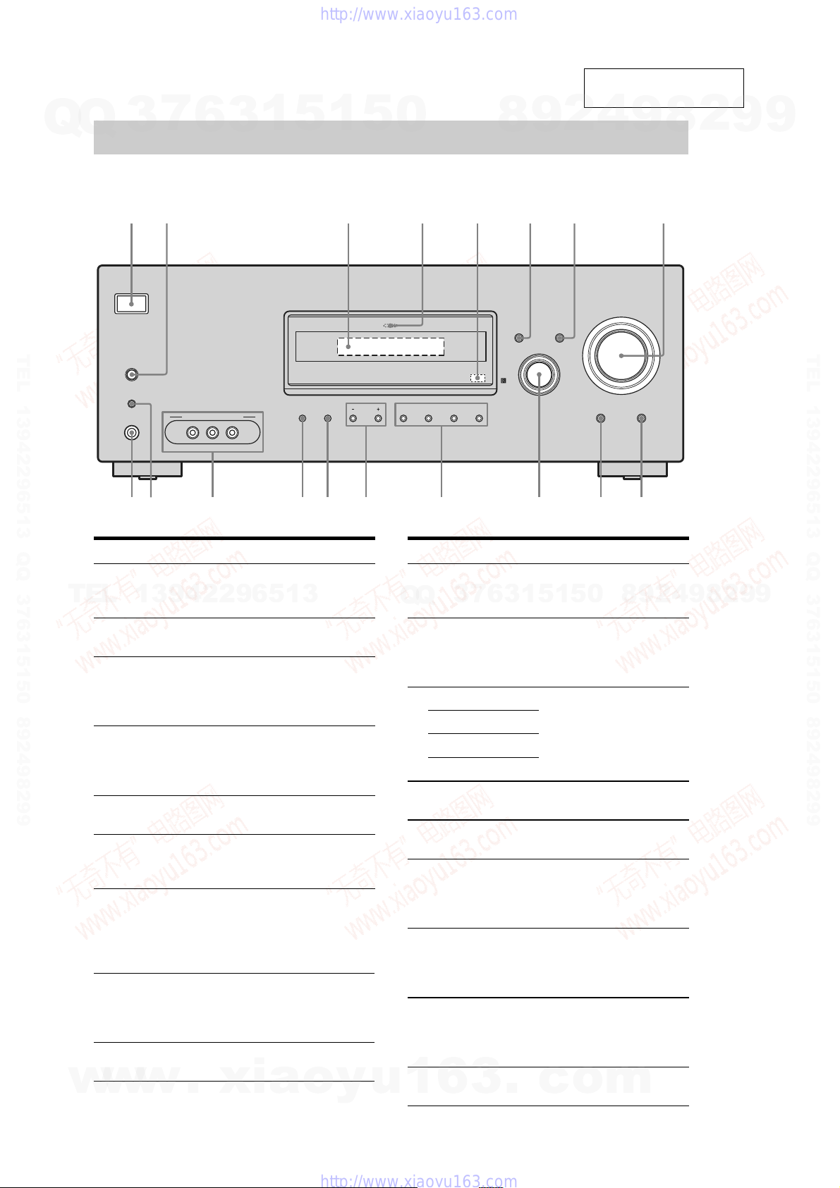
Receiver
Front panel
12 8
?/1
SPEAKERS
(OFF/A/B/A+B)
AUTO CAL MIC
PHONES
6
VIDEO 3 IN/PORTABLE AV IN
VIDEO L AUDIO R
3
1
5
MEMORY/
ENTER
1
5
0
3 5
MULTI CHANNEL DECODING
TUNING
MODE
TUNING 2CH A.F.D. MOVIE MUSIC
qs
9
8
6 74
DISPLAY INPUT MODE
INPUT SELECTOR
2
4
9
MASTER VOLUME
AUTO CAL MUTING
9
q;qaqk qdqfqgqhqj
8
2
9
9
TEL 13942296513 QQ 376315150 892498299
Name Function
A ?/1
TEL
w
(on/standby)
13942296513
B SPEAKERS
(OFF/A/B/A+B)
C Display The current status of the
D MULTI
CHANNEL
DECODING
lamp
E Remote sensor Receives s ignals from
F DISPLAY Press to select information
G INPUT MODE Press to select the input
H MASTER
VOLUME
I MUTING Press to mute the sound
w
w
.
xia
Press to turn the receiver o n
or off (page 28, 37, 38, 54,
77).
Press to select the front
speaker system (page 29).
selected component or a
list of sele ctable item s
appears here (pag e 7).
Lights up when multi
channel audio is decoded
(page 38).
remote commander.
displayed on the display
(page 64).
mode when the same
components are co nnected
to both digital and ana l og
jacks (page 59).
Turn to adjust the volume
level of all speakers at the
same time (page 34, 35, 37,
38).
(page 35).
o
y
Name Function
J AUTO CAL Press to activate the Auto
Q
K INPUT
SELECTOR
L 2CH Press to select a sound field
A.F.D.
MOVIE
MUSIC
M TUNING +/– Press to scan a station
N TUNING MODE Press to select the tunin g
O MEMORY/
ENTER
P VIDEO 3 IN/
PORTABLE AV
IN jacks
Q AUTO CAL MIC
jack
R PHONES jack Connec ts to hea dphones
u
1
6
3
(page 30).
Turn to select the input
source to playback (page
35, 37, 38, 55, 58, 59, 61,
63, 65).
(page 49, 51, 53).
(page 55, 58).
mode (page 55, 77).
Press to store a station or
enter the selection w hen
selecting the settings (page
28).
Connect to a portable
audio/video component
such as a camcorder or
video game (page 26, 35).
Connects to the supplied
optimizer micropho ne for
the Auto Calibration
function (page 30).
.
c
(page 74).
Calibration function
5
1
3
6
7
3
Q
1
0
5
o
9
8
m
2
4
9
8
2
9
9
4
STR-K995
7
Q
Q
TEL 13942296513 QQ 376315150 892498299
TEL
w
3
13942296513
w
w
6
About the indicators on the display
1 2 3 4 6 7 985
LFE
SW
LC
SL S
Name Function
A SW Lights up when the audio signal
B LFE Lights up when th e disc being
C SP A/SP B Lights up according to the
D ;D Lights up when Dolby Digital
E ;PL/
;PL II
F OPT Lights up when INPUT MODE
G DTS Lights up when DTS signals are
.
1
3
SP A
SP B
R
SR
is output fro m the SUB
WOOFER jack.
played back contains an LFE
(Low Frequency Effect)
channel and the LFE c h annel
signal is actually being
reproduced.
speaker system used. However,
these indicat o rs d o not light up
if the speaker output is turned
off or if headphones are
connected.
signals are input.
Note
When playing a Dolby Digital
format disc, be sure that you
have made digital connections
and that INPUT MODE is not
set to “ANALOG” (page 59).
“; PL” lights up when the
receiver applie s Pro Logic
processing to 2 channel signals
in order to output the center and
surround channel signals.
“; PL II” lights up when the
Pro Logic II Movie or Music
decoder is activa te d.
is set to “AUTO IN” and the
source signal is a digital signal
being input through the
OPTICAL jack, or when
INPUT MODE is set to “O PT
IN” (page 59).
input.
Note
When playing a DTS format
disc, be sure that you have made
digital connections and that
INPUT MODE is not set to
“ANALOG” (page 59).
xia
5
D
;
o
1
5
0
PL II OPT DTS MEMORY ST
;
y
u
;
Q
Q
1
PL
COAXHDMI
Name Function
H MEMORY Lights up when a memory
I Tuner
indicators
J Preset
station
indicators
K D.RANGE Lights up when dynamic range
7
3
L COAX Lights up when INPUT MODE
M HDMI Lights up when the receiver
N Playback
channel
indicators
L
R
C
SL
SR
S
6
3
8
6
3
.
4
2
9
function, such as Preset
Memory (page 57), etc., is
activated.
Lights up when using the
receiver to tune in radio stations
(page 54), etc.
Lights up when using the
receiver to tune in radio stations
you have preset. For details on
presetting radio stations, see
page 56.
compression is activated (page
42).
8
0
5
1
5
1
is set to “AUTO IN” and the
source signal is a digital signal
being input through the
COAXIAL jack, or when
INPUT MODE is set to “COAX
IN” (page 59).
recognizes a component
connected via a HD MI IN ja ck
(page 20).
The letters (L, C, R, etc.)
indicate the ch annels being
played back. The boxes around
the letters vary to show how the
receiver downmixes the source
sound.
Front Left
Front Right
Center (monaural)
Surround Left
Surround Right
Surround (monaural or the
surround component s obt ai ne d
by Pro Logic processing)
Example:
Recordin g forma t (Fro nt/
Surround): 3/2.1
Sound Field: A.F.D. AUTO
SW
L C R
SL SR
c
o
m
9
9
8
2
q;qaqf qsqd
4
MONOD.RANGE
9
2
8
9
2
9
9
TEL 13942296513 QQ 376315150 892498299
9
5
STR-K995
7
Q
Q
TEL 13942296513 QQ 376315150 892498299
TEL
3
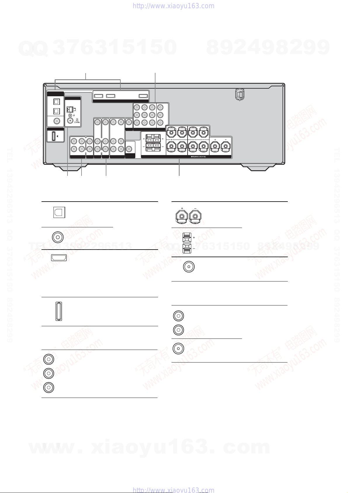
Rear panel
DIGITAL
(ASSIGNABLE)
OPTICAL
SAT
IN
VIDEO 2/
BD IN
COAXIAL
DVD
IN
DMPORT
A DIGITAL INPUT/OUTPUT sec t ion
13942296513
B COMPONENT VIDEO INPUT/
OUTPUT section
Green
(Y)
Blue
B/CB)
(P
Red
(P
R/CR)
6
ANTENNA
AM
L
R
OUT IN
SA-CD/CD/CD-R
5
6
OPTICAL
IN jack
COAXIAL IN
jack
HDMI IN/
OUT jack
DMPORT
jack
COMPONENT
VIDEO
INPUT/
OUTPUT
jack
1
L
R
IN
TV
a)
1
5
1
3
DVD IN
VIDEO 2/BD IN
HDMI
VIDEO OUT
VIDEO IN
AUDIO IN
SAT
L
R
a)
VIDEO IN
VIDEO OUT
VIDEO IN
AUDIO IN
DVD
43
MONITOR
L
AUDIO OUT
R
AUDIO IN
AUDIO OUT
SUB
WOOFER
VIDEO 1
Connects to a DVD
player, etc. The
COAXIAL jack
provides a better
quality of loud
sound (page 23,
25).
Connects to a DVD
player, or a Blu-ray
disc player. The
image and the
sound are output to
a TV or a projector
(page 20).
Connect to a
DIGITAL MEDIA
PORT adapter
(page 60).
Connects to a DVD
player, TV,
satellite tuner, etc.
You can enjoy high
quality image
(page 22, 23, 25).
5
OUT
SAT IN
DVD IN VIDEO 1 IN
COMPONENT VIDEO
FRONT B
2
0
Y
P
B/CB
PR/C
R
MONITOR OUT
LR
LL
R
FRONT A
SPEAKERS
C SPEAKERS section
Q
Q
D VIDEO/AU DIO INPUT/OUTPUT
SURROUND
7
3
section
White (L)
Red (R)
Yellow
R
8
CENTER
1
3
6
AUDIO IN/
OUT jack
VIDEO IN/
OUT jack
9
5
4
2
Connects to
speakers (page 17).
0
5
1
Connects to sub
woofer (page 17).
Connects the video
and audio jacks of a
VCR, a DVD
player, etc.
(page 22–26).
a)
9
8
9
8
2
4
2
9
8
9
2
9
9
TEL 13942296513 QQ 376315150 892498299
9
6
w
w
w
.
xia
o
y
u
1
6
3
.
c
o
m
a)
You can watch the sele cted inp ut imag e when yo u
connect the HDMI OUT or MONITOR OUT jack
to a TV (page 22).
You can use the supplied remote to operate the
receiver and to control the Son y audio/video
components that the remote is assigned to
operate.
You can also program the remote to control
non-Sony audio/video components. For
details, see “Programming the remote” (page
66).
RM-AAP017
E AUDIO INPUT/OUTPUT section
AUDIO IN/
OUT jack
Connects to Super
Audio CD player,
CD player, etc.
(page 18).
F ANTENNA section
FM
ANTENNA
jack
Connects to the FM
wire antenna
supplied with this
receiver (page 27).
AM
ANTENNA
terminals
Connects to the AM
loop antenna
supplied with this
receiver (page 27).
White (L)
Red (R)
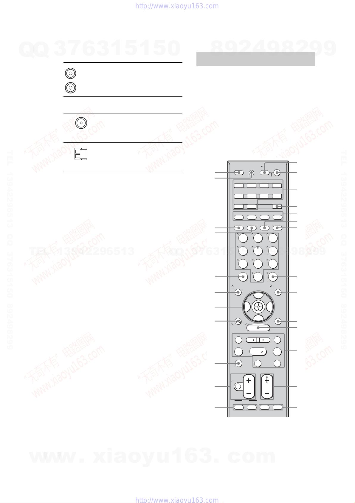
Remote commander
SYSTEM STANDBY
TUNING –
DISC SKIP
MUTING
TOP MENU MENU F1
TV INPUT WIDE
F2
TV VOL
MASTER VOL
TV CH
PRESET
TUNING +
GUIDE
DISPLAY
RETURN/
EXIT
OPTIONS
TOOLS
REPLAY ADVANCE
TV
VIDEO 1 VIDEO 2 VIDEO 3 DVD
SAT TV TUNER
2CH A.F.D. MOVIE MUSIC
SLEEP
FM MODE D. TUNING
SA-CD/CD
AUXDMPORT RECEIVER
RM SET UP
?/1
MEMORY
.
>
m
M
xX
MENU
H
CLEAR
>10
–/– –
<
<
DVD
23
456
789
ENTER
0/10
1
AV ?/1
AUTO CAL
B
V
v
B
1
6
2
9
q;
qa
qj
qk
ql
wa
w;
qd
qf
qg
qs
4
5
7
8
3
qh
ws
wh
wf
wd
wg
STR-K995
7
Q
Q
TEL 13942296513 QQ 376315150 892498299
TEL
3
13942296513
6
3
1
5
1
5
0
Q
Q
7
3
8
3
6
9
1
5
2
1
5
4
0
9
8
9
8
2
4
2
9
8
9
2
9
9
TEL 13942296513 QQ 376315150 892498299
9
w
w
w
.
xia
o
y
u
1
6
3
.
c
o
m
7
STR-K995
7
Q
Q
TEL 13942296513 QQ 376315150 892498299
TEL
3
Name Function
A AV ?/1
(on/standby)
B ?/1
(on/standby)
C Input
buttons
13942296513
6
Press to turn on or off the
audio/video com ponents that
the remote is programmed to
operate.
To turn the TV on or off, press
TV (Z) and then press AV
?/1.
If you press ?/1 (B) at the
same time, it will turn off the
receiver and other components
(SYSTEM STANDBY).
Note
The function of the AV ?/1
switch changes automatically
each time you press the input
buttons (3).
Press to turn th e r e ceiver on or
off.
To turn off all components,
press ?/1 and AV ?/1 (A) at
the same time (SYSTEM
STANDBY).
Press one of the buttons to
select the comp onent you want
to use. When you press any of
the input buttons, the receiver
turns on. The but tons are
factory assigned to control
Sony components as follows.
You can program the remote to
control non-So ny components
following the steps in
“Programming the remote” on
page 66.
Button Assigned Sony
VIDEO 1 VCR (VTR mode 3)
VIDEO 2 VCR (VTR mode 2)
VIDEO 3 VCR (VTR mode 1)
DVDDVD player
SATSatellite tuner
TV TV
SA-CD/CD Super Audio CD/
TUNER Built-in tuner
AUXNot assigned
DMPORT DIGITAL MEDIA
3
1
5
component
CD player
PORT adapter
1
5
0
Name Function
D RECEIVER Press to activate the receiver
E 2CH Press to select a sound field
A.F.D.
MOVIE
MUSIC
F D. TUNING Press to enter direct tuning
G AUTO CAL Pr ess to activate the Auto
H Numeric
buttons
(number 5
7
3
Q
Q
I ENTER Press to enter the v alue after
MEMORY Press to store a station during
J DISPLAY Press to select inf or mation
4
2
9
8
operation (page 39).
(page 49, 51, 53).
mode.
Calibration function.
Press to
–preset/tune to preset stations.
a)
)
–select track numbers of the
CD player, VCD player, LD
player, DVD player, MD
deck, DAT deck, or tape deck.
Press 0/10 to select track
number 10.
–select chann el numb ers o f th e
VCR, satellite tuner, Blu-ray
disc recorder, PSX, DVD/
VHS COMBO or DVD/HDD
COMBO.
Press TV (Z) and then press
the numeric b uttons to sele ct
the TV channels.
5
1
3
6
selecting a channe l, disc or
track using the nu meric bu ttons
of the VCR, CD player, V C D
player, LD player, MD deck,
DAT deck, tape deck, satellite
tuner, Blu-ray disc recorder or
PSX.
To enter the value of Sony TV,
press TV (Z) and then press
ENTER.
tuner operation.
displayed on the TV screen of
the VCR, VCD player, LD
player, DVD player, CD player,
MD deck, Blu-ray disc
recorder, PSX, satellite tuner,
DVD/VHS COMBO or DVD/
HDD COMBO.
To select information of Sony
TV, press TV (Z) and then
press DISPLAY.
1
5
0
9
8
9
8
2
4
2
9
8
9
2
9
9
TEL 13942296513 QQ 376315150 892498299
9
8
w
w
w
.
xia
o
y
u
1
6
3
.
c
o
m

STR-K995
7
Q
Q
TEL 13942296513 QQ 376315150 892498299
TEL
3
K OPTIONS
L MENU Press to display the menus of
M H
13942296513
6
Name Function
TOOLS
a) b)
b)
X
b)
x
m/M
1
5
3
Press to display and select items
from the option menus for DVD
player or DVD/VHS COMBO.
To display the options of Sony
TV, press TV (Z) and then
press OPTIONS TOOLS.
the receiver, VCR, DVD
player, satell ite tuner, B lu-ray
disc recorder, PSX, DVD/VHS
COMBO or DVD/HDD
COMBO on the TV screen.
Then, use V/v/B/b and to
perform menu operations.
To display the menus of Sony
TV, press TV (Z) and then
press MENU.
Press to start playback of the
VCR, CD player, VCD player,
LD player, DVD player, MD
deck, DAT deck, tape deck,
Blu-ray disc recorder, PSX,
DVD/VHS COMBO or DVD/
HDD COMBO.
Press to pause playback or
recording of th e VCR, CD
player, VCD player , LD pl ayer,
DVD player, MD deck, DAT
deck, tape deck, Blu-ray disc
recorder, PSX, DVD/VHS
COMBO or DVD/HDD
COMBO. (Also starts
recording with comp on en ts in
recording standby.)
Press to stop playback of the
VCR, CD player, VCD player,
LD player, DVD player, MD
deck, DAT deck, tape deck,
Blu-ray disc recorder, PSX,
DVD/VHS COMBO or DVD/
HDD COMBO.
b)
Press to
–search tracks in the forward/
backward di rectio n of the CD
player, VCD player, DVD
player, LD player, MD deck,
Blu-ray disc recorder, PSX,
DVD/VHS COMBO, or
DVD/HDD COMBO.
–fast forward/rewind of the
VCR, DAT deck, or tape
deck.
1
5
0
Q
Q
Name Function
N TV CH +
O F1, F2 Press F1 or F2 to select a
7
3
P DVD TOP
4
2
9
8
/–
3
b)
Press to skip tracks of the
VCR, CD player, VCD player,
LD player, DVD player, MD
deck, DAT deck, tape deck,
Blu-ray disc recorder, PSX,
DVD/VHS COMBO or DVD/
HDD COMBO.
Press to replay the previous
scene or fast forward the
current scene of the DVD
player, Blu-ray di sc recorder,
DVD/VHS COMBO or DVD/
HDD COMBO.
a)
/– Press TV (Z) and then press
TV CH +/– to select preset TV
channels.
Press to
–select preset stations.
–select preset channels of the
VCR, satellite tun er, Blu- ray
disc recorder, DVD player,
DVD/VHS COMBO or
DVD/HDD COMBO.
component.
0
5
1
5
1
– DVD/HDD COMBO
F1: HDD mode
F2: DVD mode
– DVD/VHS COMBO
F1: DVD mode
F2: VHS mode
TV INPUT to select the input
signal (TV input or video
input).
WIDE to select the wide
picture mode.
Press to display the menu or
on-screen guide of the DVD
player on the TV screen.
Then, use V/v/B/b and to
perform menu operations.
the DVD player on the TV
screen. Then, u se V/v/B/b and
operations.
./>
TUNING +/– Press to scan a station.
REPLAY /
ADVANCE
PRESET
a)
+
6
TV INPUT Press TV (Z) and then press
WIDE Press TV (Z) and then press
MENU
DVD MENU Press to display the menu of
9
2
9
8
to perform menu
8
4
2
9
8
2
9
9
9
TEL 13942296513 QQ 376315150 892498299
9
w
w
w
.
xia
o
y
u
1
6
3
.
c
o
m
9
STR-K995
7
Q
Q
TEL 13942296513 QQ 376315150 892498299
TEL
w
3
Name Function
Q TV VOL +/– Press TV (Z) and then press
MASTER
VOL +/–
MUTING Press to mute the sound
R DISC SKIP Press to skip disc of the CD
S RETURN/
EXIT O
13942296513
T
V/v/B/b
U GUIDE Press to display the EPG
w
w
6
TV VOL +/– to adjust the TV
volume level.
Press to adjust the volume
level of all speakers at the
same time.
(page 35).
To mute the sound of the TV,
press TV (Z) and then press
MUTING.
player, VCD player, DVD
player or MD deck (multi-disc
changer only).
Press to
–return to the previous menu.
–exit the menu while the
To return to the previous
menu of Sony TV, press TV
(Z) and then pres s
RETURN/EXIT O.
After pressing RECE IV ER
(D), press MENU (L) for
receiver operation, then press
V/v/B/b to sel ect th e s ettin gs.
After pressing DVD TOP
MENU (P) or DVD MENU
(P), press V/v/B/b to select
the settings, and then press
Press also to enter the
selection of the receiver,
VCR, satellite tuner, DVD
player, Blu-ray disc record er,
PSX, DVD/VHS COMBO or
DVD/HDD COMBO.
(Electronic Program Guide)
of the TV, DVD player,
satellite tuner, Blu-ray disc
recorder, PSX or DVD/HDD
COMBO.
.
1
5
o
1
y
3
menu or on-screen guide of
the VCD player, LD player,
DVD player, Blu-ray disc
recorder, PSX, DVD/VHS
COMBO or satellite tuner is
displayed on the TV screen.
to enter the selection.
xia
5
u
0
Name Function
V -/-- Press to select the channel
CLEAR Press to clear a mistake when
>10 Press to select track numbers
W FM MODE Press to select FM mona ural
X SLEEP Press to activate the Sleep
Y RM SET UP Press to set up the remote.
7
3
Q
Q
Z TV Press to light up the button. It
a)
The number 5, PRESET +, TV CH + and H
buttons have tactile dots. Use the tactile dots as
references when operating the re ceiver.
b)
The button is also availa ble for DIGITAL MEDIA
PORT adapter operation. For details on the
function of the button, see the ope rating
instructions supplied with the DIGITAL MEDIA
PORT adapter.
Notes
Some functions explained in this section may not
work depending on the mo de l.
The above explanation is intended to serve as an
example only. Therefore, depending on the
component, the ab ove operation may no t be
possible or may operate differently than described.
The AUX button on the remote is not av aila ble for
receiver opera tion.
1
6
3
4
2
9
8
entry mode, either one or two
digit of the VCR or satellite
tuner.
To select the channel entry
mode of the TV, press TV
(Z) and then press -/--.
you press the incorre ct
numeric button of the DVD
player, Blu-ray di sc recorder,
PSX, satellite tuner, DVD/
VHS COMBO or DVD/HDD
COMBO.
over 10 of the CD player,
VCD player, LD player, MD
deck, tape deck, TV, VCR or
satellite tuner.
or stereo reception.
Timer function and the
duration which the receiver
turns off automatically.
0
5
1
5
1
3
6
changes the remote key
function to activate the
buttons with orange printing.
It also activate the DISPLAY
(J), OPTIONS TOOLS
(K), MENU (L),
RETURN/EXIT O (S),
(T) and V/v/B/b (T)
buttons to perform menu
operations for Sony TVs only.
.
c
o
9
9
8
m
8
2
4
2
9
8
9
2
9
9
TEL 13942296513 QQ 376315150 892498299
9
10
SPK Front Left
DCAC MIC
Receiver
SECTION 2
TEST MODE
STR-K995
7
3
Q
TEL 13942296513 QQ 376315150 892498299
SOUND FIELD CLEAR MODE
Q
The preset sound field is cleared when this mode is activated. Use
this mode before returning the product to clients upon completion
of repair.
Procedure:
1. While depressing the 2CH button, press the power ?/1
button to turn on the main power.
2. The message “S.F. CLR.” appears and initialization is
performed. (3 second)
SOFTWARE VERSION DISPLAY MODE
The software version is displayed.
Procedure:
1. While depressing the SPEAKERS (OFF/A/B/A+B) and the
DISPLAY buttons simultaneously, press the power ?/1
button to turn on the main power.
2. The model name, destination and the software version are
displayed. (8 second)
KEY CHECK MODE
Button check
Procedure:
1. While depressing the SPEAKERS (OFF/A/B/A+B) and the
2CH buttons simultaneously , press the power ?/1 button to
turn on the main power.
“REST 13” appears.
2. Every pressing of any button other than ?/1 counts down
the buttons. The buttons which are already counted once are
not counted again.
3. When all buttons are pressed “REST 00” appears.
TEL
13942296513
FLUORESCENT INDICATOR TUBE TEST MODE
All fluorescent segments are tested. When this test is acti v ated, all
segments turn on at the same time, then each segment turns on one
after another.
Procedure:
1. While depressing the TUNING MODE and the DISPLAY
buttons simultaneously, press the power ?/1 button to turn
on the main power.
2. All segments turn on.
• Blue LED of MULTI CHANNEL DECODING lights.
LFE
SW
L C R
SLSSR
SB SBRSBL
SP A
SP B
;
6
D EX
;
1
OPT
5
DTS-ES 96 / 24
3
MULTI CHANNEL DECODING
PL II x;PL
HDMI COAX
1
Blue LED
NEO:6 SAT D.RANGE
CAT
5
MEMORY
dB
k Hz
mft.
MHz
0
Q
Q
RDS ST
MONO
5. Turn the INPUT SELECTOR dial once again. All segments
6. Every turning of the INPUT SELECTOR dial turns on each
SWAP ALL MODE
The signal will be swapped to all channels so that all speakers will
have sound output.
Procedure:
1. While depressing the SPEAKERS (OFF/A/B/A+B) and the
2. “SWAP” appears. (No change while displayed.)
SHIPMENT MODE
All preset contents are reset to the default setting.
Procedure:
1. While depressing the SPEAKERS (OFF/A/B/A+B) and the
2. “CLEARED” appears and switch off the set.
PROTECTOR
If an error occurs, the “Protector Display” will flash for a while and
the power is turned OFF.
Procedure:
1. While depressing the TUNING – and the A.F.D. buttons
2. “PROTEVER” appears (3 seconds).
7
3
DCAC FACTORY TEST MODE
DCAC Factory Test mode have two stages:
1. DCAC DSP Data Line Checking
2. DCAC board Checking
Factory Test System Setup
4
2
9
8
turn off.
segment one after another in the same order.
A.F .D. buttons simultaneously, press the power ?/1 button
to turn on the main power.
MUSIC buttons simultaneously, press the power ?/1 but-
ton to turn on the main power.
simultaneously, press the power ?/1 button to turn on the
main power.
0
5
1
5
1
3
6
Start Pass Pass
DSP Data Line
Check
9
8
9
2
Auto Cal Mic
8
4
Check
2
9
8
9
2
9
9
9
END
TEL 13942296513 QQ 376315150 892498299
3. Turn the INPUT SELECTOR dial.
• Blue LED of MULTI CHANNEL DECODING is turned off.
MULTI CHANNEL DECODING
LFE
SP B
L R
S
4. Turn the INPUT SELECTOR dial once again.
• Blue LED of MULTI CHANNEL DECODING lights.
LFE
SPA
w
w
SPB
w
.
x
MULTI CHANNEL DECODING
EX
;
PL ll X
HDMI COAX
xia
OPT
Blue LED
NEO:6 D.RANGE MONOCOAX
Blue LED
CAT
96/24
-ES
SAT
NEO:6
o
y
k
m
MHz
MEMORY
D.RANGE
u
dB
Hz
ft.
RDS
ST
MONO
1
1. When power off :
Press the three buttons MEMORY/ENTER + MOVIE +
?/1 .
“DCAC[]FTM” appears.
Afterward, press the TUNING MODE to start DCAC f actory
test mode.
6
3
.
c
o
m
11
STR-K995
1.DCAC DSP Data Line Checking
Q
Q
After press the TUNING MODE , DCAC Factory test mode will
start, below display will show:
“DCAC[][][]x” x = 1, 2, 3, 4
If there is error happen, below display will show:
“ERR[]SD0x” x = 1 → D1501 or R1530
2.DCAC board Checking
Connect front left speaker of the receiver and AUTO CAL
microphone. Turn MASTER V OLUME jog, there will be test tone
sound output from front left speaker, and the display will change
TEL 13942296513 QQ 376315150 892498299
accordingly.
“AD[]-[]xxx” xxx = 0 to 255 (depends on loudness of test tone)
VACS CONTROL
The VACS feature of the amplifier is turned off purposely.
Procedure:
1. While depressing the MEMORY/ENTER and the 2CH
buttons simultaneously, press the power ?/1 button to turn
on the main power.
2. “VACS OFF” appears. (8 second)
7
3
x = 2 → D1502 problem
x = 3 → D1503 problem
x = 4 → D1504 problem
6
3
1
5
1
5
0
8
9
2
4
9
8
2
9
9
TEL 13942296513 QQ 376315150 892498299
AM CHANNEL STEP 9 kHz/10 kHz
SELECTION MODE
• Either the 9 kHz step or 10 kHz step can be selected for the
AM channel step.
TEL
• Procedure:
Set the FUNCTION to AM. Turn off the main power.
While depressing the TUNING MODE button, press the
power ?/1 button to turn on the main power. Either the
message “9 k STEP” or “10 k STEP” appears. Select the
desired step.
BLUE LED TEST MODE
• LED illumination check
Procedure:
1. While depressing the TUNING MODE and INPUT MODE
simultaneously, press ?/1 . Then, “B. LED ON” or “B. LED
OFF” is displayed.
2. When “B. LED ON” is displayed, the LED of the “MULTI
CHANNEL DECODING” area at the top of the display
illuminates.
13942296513
Q
Q
3
7
6
3
1
5
1
5
0
8
9
2
4
9
8
2
9
9
12
w
w
w
.
xia
o
y
u
1
6
3
.
c
o
m
SECTION 3
ELECTRICAL ADJUSTMENT
STR-K995
7
Q
Q
TEL 13942296513 QQ 376315150 892498299
3
TUNER SECTION
[FM Auto Stop Check]
SET
Procedure:
1. Turn the power on.
2. Input the following signal from Signal Generator to FM
antenna input directly.
* Carrier Freq: A = 87.5 MHz, B = 98 MHz, C = 108 MHz
Deviation : 75 kHz
Modulation : 1 kHz
ANT input : 35 dBu (EMF)
Note: Please use 75 ohm “coaxial cable” to connect SG and the set. You
cannot use video cable for checking.
Please use SG whose output impedance is 75 ohm.
6
3
1
5
1
OUT (75
5
generator
Ω
)
0
8
9
2
4
9
8
2
9
9
TEL 13942296513 QQ 376315150 892498299
3. Set to FM tuner function and scan the input FM signal with
automatic scanning.
4. Confirm that input Frequency of A, B and C are detected and
TEL
automatic scanning stops.
13942296513
The stop of automatic scanning means “The station signal is received
in good condition.”
Q
Q
3
7
6
3
1
5
1
5
0
8
9
2
4
9
8
2
9
9
w
w
w
.
xia
o
y
u
1
6
3
.
c
o
m
13
STR-K995
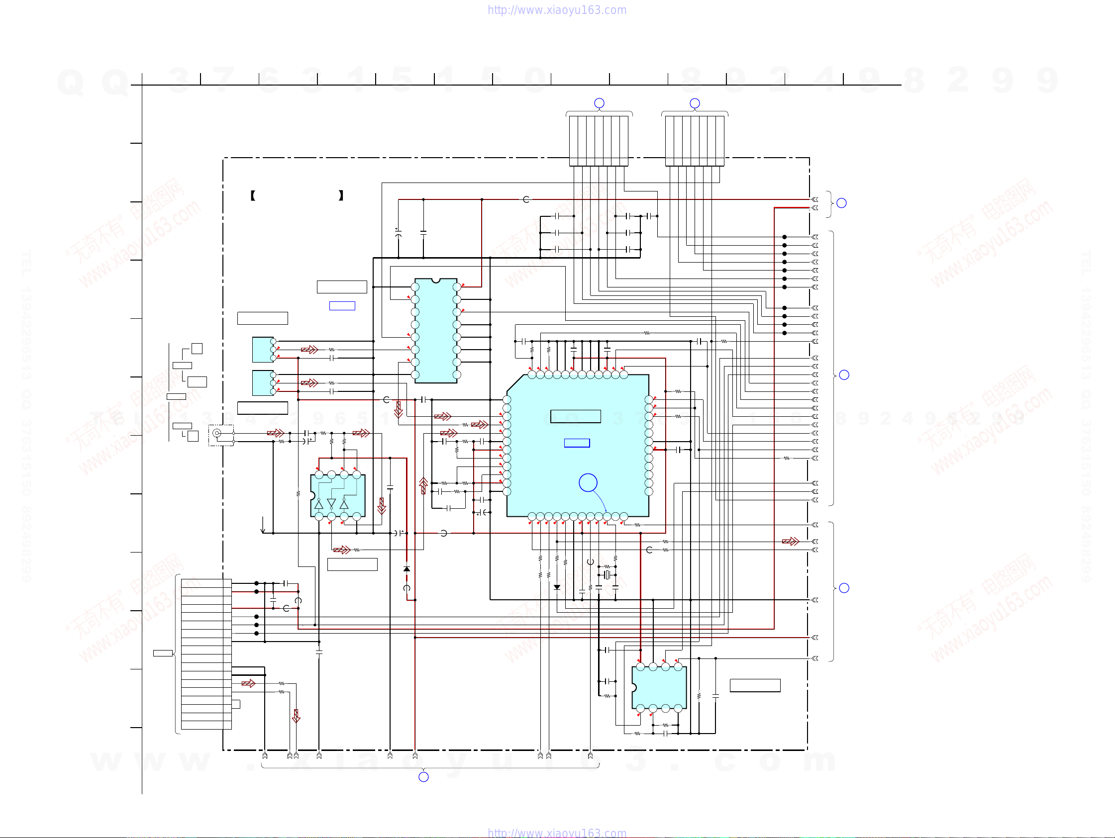
SECTION 4
DIAGRAMS
THIS NOTE IS COMMON FOR PRINTED WIRING BOARDS AND SCHEMATIC DIAGRAMS.
(In addition to this, the necessary note is printed in each block.)
Q
Q
3
7
6
3
1
5
1
5
0
8
9
2
4
9
8
2
9
9
For Schematic Diagrams.
Note:
• All capacitors are in µF unless otherwise noted. (p: pF)
50 WV or less are not indicated except f or electrolytics and
tantalums.
• All resistors are in Ω and 1/
specified.
• % : indicates tolerance.
• f : internal component.
• 2 : nonflammable resistor.
• 5 : fusible resistor.
• C : panel designation.
Note: The components identified by mark 0 or dotted
TEL 13942296513 QQ 376315150 892498299
• A : B+ Line.
• B : B– Line.
•Voltages and w av ef orms are dc with respect to ground un-
•Voltages are taken with a VOM (Input impedance 10 MΩ).
•Waveforms are taken with a oscilloscope.
• Circled numbers refer to waveforms.
• Signal path.
line with mark 0 are critical for safety.
Replace only with part number specified.
der no-signal (detuned) conditions.
No mark : FM
Voltage variations may be noted due to normal production
tolerances.
F : FM
J : ANALOG
c : DIGITAL
I : VIDEO
4
W or less unless otherwise
For Printed Wiring Boards.
Note:
• X : parts extracted from the component side.
• a: Through hole.
• f : internal component.
• : Pattern from the side which enables seeing.
Caution:
Pattern face side: Parts on the pattern face side seen from
(Side B) the pattern face are indicated.
Parts face side: P arts on the parts face side seen from
(Side A) the parts face are indicated.
• Indication of transistor.
C
Q
B
E
B
These are omitted.
CE
TEL 13942296513 QQ 376315150 892498299
These are omitted.
TEL
• Circuit Boards Location
13942296513
POWER KEY board
DCAC board
HEADPHONE board
STANDBY board
VIDEO 3 board
Q
DCDC board
DISPLAY board
Q
3
6
7
3
HDMI RE board
MAIN board
1
5
1
VIDEO board
8
0
5
DIGITAL board
9
2
4
9
8
2
9
9
14
w
w
w
.
xia
o
y
u
1
6
3
.
c
o
m
STR-K995
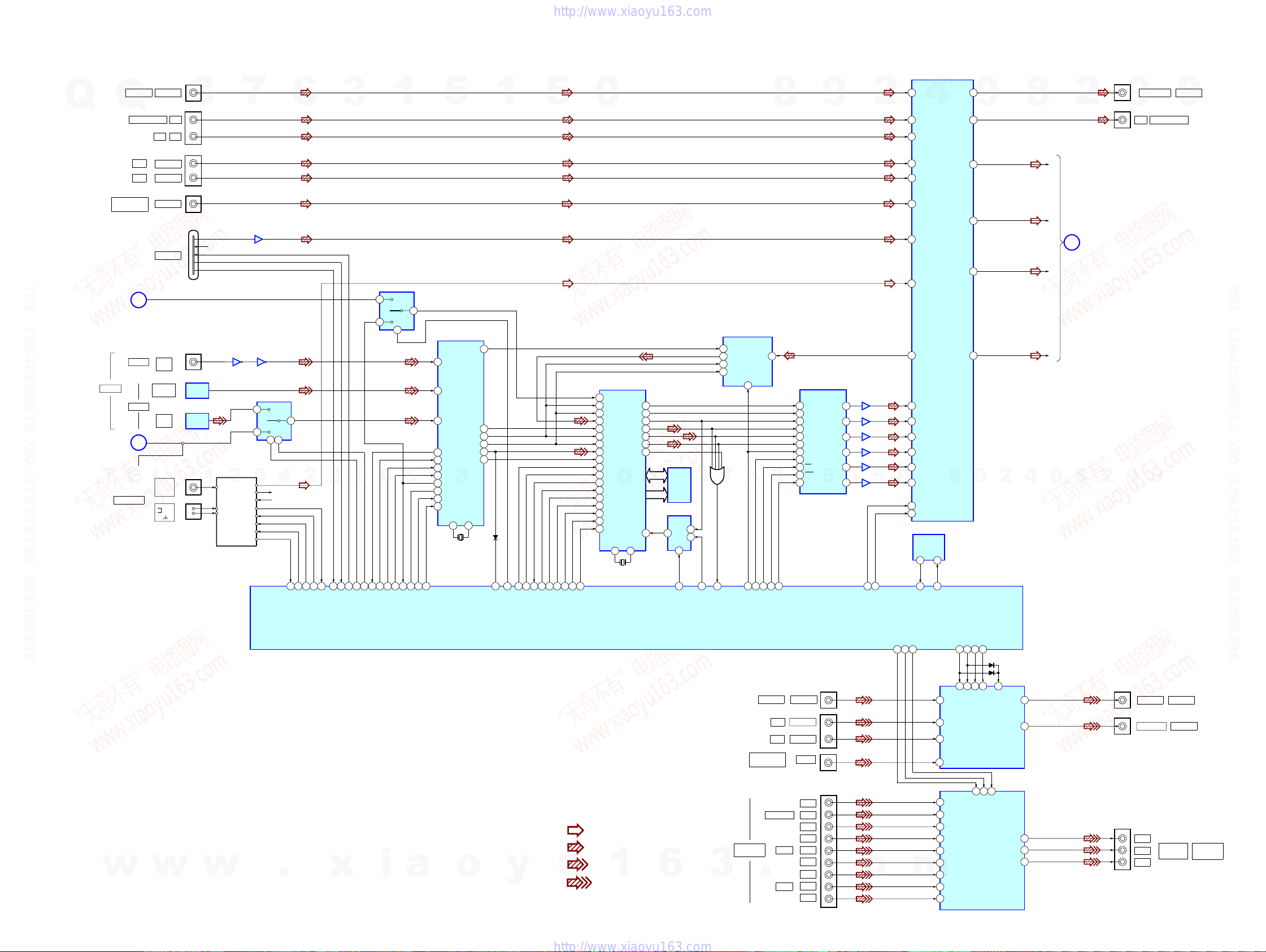
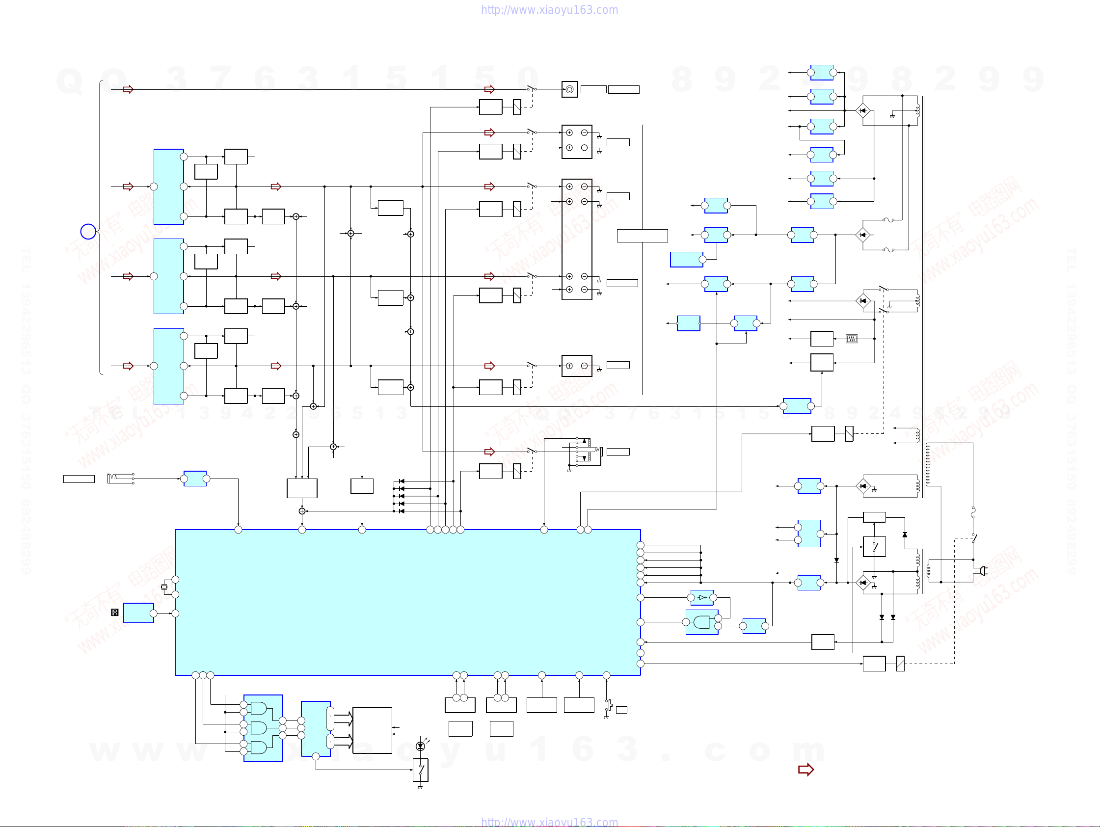
4-1. BLOCK DIAGRAM – MAIN SECTION –
J402(1/2)
VIDEO 1
AUDIO IN
Q
Q
SA-CD/CD/CD-R
SAT
DVD
VIDEO 3 IN/
PORTABLE AV IN
J405 (1/2)
TV
J403 (1/2)
AUDIO IN
AUDIO IN
J298(1/2)
AUDIO
DMPORT
J1311
3
IN
IN
13
L
C LINK_TX
6
5
C LINK_RX
7
DET
TEL 13942296513 QQ 376315150 892498299
HDMI
SECTION
(Page 17)
DIGITAL
HDMI
SECTION
(Page 17)
T
ANTENNA
COAXIAL
OPTICAL
SPDIF
E
HDMI_MUTE
C
J1301
DVD
IN
BD IN
SAT
IC1351
OPTICAL
IN
IC1354
OPTICAL
IN
IN
VIDEO 2/
B
L
COAXIAL
FM
75Ω
AM
1
7
DMPORT+5V,VBUS+5V
IC1303
35
TN1
TUNER PACK
3
L CH
FM
R CH
AM
CLK
IC3002
31
IC1303
62
6
5
9
DO
DI
CE
SD
IC1302
2 14
R-CH
TUNER +10V10V
4
6
7
27
117
TUNER SD
2
79
TUN_LAP
TUNER_CLK
26
80
TUN_DO
TUNER_DATA
2
104
3
102
C LINK_DET
1
IC1017
2
1
6
9
6
48 4742 41 45 46 49 50 39 63
103
DIR_DI
DIR_CE
DIR_DO
DIR_CLK
TC74HC153_A
TC74HC153_B
FLASH1/C LINK_TX
FLASH2/C LINK_RX
5
5
38
DIR_ERROR
DIR_XSTATE
5
3
4
35
36
38
37
1
34
17
48
47
DIR_XMODE
DIR_CKSEL1
5
IC1301
DIGITAL AUDIO
I/F RECEIVER
XMCK
DIN2
DIN0
DIN1
CK OUT
BCK
LRCK
DATAO
DOUT
DI
CLK
CE
3
ERROR
XSTATE
XMODE
CKSEL1
XIN XOUT
22 21
X1301
12.288MHz
IC1907(1/3)
SYSTEM CONTROLLER
20
13
14
15
16
24AUDIO
D1301
1
DIR_DATA0
ERROR_SEL
IC401
ANALOG SOUND
PROCESSOR
24
34
32
30
26
28
36
38
41
49
50
51
56
53
0
54
60
59
V_COMP_SW2
V_COMP_SW1
V_MUTE
2930
28
INBL
4
INGL
INFL
INEL
INCL
INDL
INHL
INIL
AOUTL
INCL
INCSL
INCC
INCSW
INCSR
INCSL
DATA
CLK
IC1131
EEPROM
SDA SCL
5 6
97 98
EEPROM_DATA
5
101
67
74
6583
99
100
GP9
GP12
HD OUT
HD IN
HCLK
HCS
0
AD CONVERTER
15
SCK
12
DOUT
11
BCK
10
IC1501
AUDIO DSP
EXLOCK59
17
BCKI1
SCK OUT
Q
12 9
X1502
13.9MHz
BCKO
SDO1
SDO2
SDO3
SDO4
MCLK1
14
20
19LRCKO
23
24
25
26
IC1502
SRAM
IC1503
SELECTOR
556
Y
S
6
64
2
B
1
A
BST_SEL
3
Q
BST
15
LRCKI1
18 SDI1
22
KFSI0
29
BCKI2
28
LRCKI2
30
SDI2
69
GP8
68
GP9
37
GP12
35
HD OUT
33
HD IN
34
HCLK
36
HCS
32
HACN
PM
113
2
XRST
MCLK2
68
73
69
PM
HACN
DSP_RESET
LRCK
7
D1501
_
D1504
66
87
BST
DCAC_DSP_IN
IC1401
RST
7
6
37
27
PCM1609_ML
PCM1609/_RESET
VIDEO 3 IN/
PORTABLE AV IN
8
LIN
1
3
5
4
PCM1609_MC
PCM1609_MDI
VIDEO 1
SAT
DVD
75
PCM1609_MDO
38
40
41
47
45
46
37
36
35
34
1
33
J201
(1/2)
VIDEO IN
J200(1/2)
VIDEO IN
VIDEO IN
J298(2/2)
VIDEO
IC1452
AUDIO CODEC
SCKI
BCK
LRCK
DATA3
DATA1
DATA2
RST
ML
MC
MDI
MDO
9
VOUT5
VOUT6
VOUT3
VOUT4
VOUT2
5
VOUT1
10
12
11
13
14
9
1
2
IC1403
31
IC1403
57
IC1404
31
IC1404
57
IC1405
31
IC1405
57
5
10
11
VOL_DA
VOL_CL
ROUTAL
ROUTBL
OUT SL
OUTSW
8
EEPROM_CLK
13
V1
3
SAT
5
DVD
9
V3
44
9
46
OUT L
88
85
OUTC
86
81
9
V_SW1
V_SW3
V_SW4
V_SW2
31 3332
34
14
10
SW14SW36SW42SW5
SW2
IC203
VIDEO AMP
2
D204
D203
M.OUT
V1OUT
8
4
1
15
L
SL
SL
C
SW
9
2
A
(Page 16)
8
DISPLAY
/POWER
SECTION
2
J402
(2/2)
9
J405
(2/2)
OUT
9
VIDEO OUT
VIDEO OUT
AUDIO OUT
SA-CD/CD/CD-R
9
J201(2/2)
J200(2/2)
VIDEO 1
9
TEL 13942296513 QQ 376315150 892498299
MONITOR
VIDEO 1
STR-K995
w
w
w
.
x
i
a
o
y
• R-CH is omitted due to same as L-CH.
• Signal Path
: FM
: ANALOG
u
: DIGITAL
1
: VIDEO
6
3
1515
COMPONENT
VIDEO
.
VIDEO 1 IN
DVD IN
SAT IN
J301
Y
P
B/CB
P
R/CR
Y
P
B/CB
P
R/CR
c
Y
P
B/CB
P
R/CR
o
1
m
5
12
CH1 IN1
CH2 IN17
CH3 IN116
CH1 IN23
CH2 IN29
CH3 IN214
CH1 IN3
CH2 IN311
CH3 IN3
4
SW12SW2
IC304
VIDEO AMP
21
P.SAVE
CH1 OUT
CH2 OUT
CH3 OUT
J302
22
20
18
Y
MONITOR
P
B/CB
P
R/CR
CONPONENT
OUT
VIDEO
STR-K995
4-2. BLOCK DIAGRAM – DISPLAY/POWER SECTION –
12
9
11
12
9
11
12
9
11-V OUT2
IC2000
AMP
5 1
X0
X1
78
Q701,702
LIMITER
Q651,652
LIMITER
Q501,502
LIMITER
3
FL_LAT
FL_CLK71FL_DATA
70
7
9
5V
Q703
BOOSTER
Q704
BOOSTER
Q653
BOOSTER
Q654
BOOSTER
Q503
BOOSTER
Q504
BOOSTER
113
4
DCAC IN
4
5
2
1
9
10
.
6
Q705,706
CURRENT
DETECT
Q655,656
CURRENT
DETECT
Q505,506
CURRENT
DETECT
2
IC101
2
Q722,723,725
6
3
8
x
3
Q793,795
PROTECT
SWITCH
12
PROTECTOR
7
8
9
R-CH
R-CH R-CH
SR-CH
9
6
R-CH
IC100
FL DRIVE
14
SEG1-17
DIN
29
31
CLK
STB
42
32
GRID1-11
SW1
1
i
Q
MAIN
SECTION
TEL 13942296513 QQ 376315150 892498299
(Page 15)
AUTO CAL MIC
SW
Q
L
A
SLSL
C
T
J2000
w
E
L
IC103
REMOTE
CONTROL
RECEIVER
w
X1101
12.5MHz
3
IC701
POWER AMP
+V OUT2
8
IN2
-V OUT2
IC601
POWER AMP
+V OUT2
IN2
8
-V OUT2
IC501
POWER AMP
+V OUT2
8
IN2
2
NF2
NF2
NF2
1
58
57
82 SIRCS IN
w
1
5
SR-CH
D841
VACS
CONTROL
119
SYSTEM CONTROLLER
FLUORESCENT
INDICATOR TUBE
a
1
VACS CTRL
IC1907 (2/3)
FL101
5
Q740
AF POWER
PROTECT
Q640
AF POWER
PROTECT
SR-CH
Q540
AF POWER
PROTECT
3
D1107
D1108
D1109
D1110
D1111
F1
F2
o
1
22
SW_RY
5V
D105
Q110
23
25
17
24
HP_RY
C/REAR/SB_RY
FRONT_A_RY/DG51_FB
FRONT_B_RY/DG51_FA
VOL_ENCODER(B)_UP
VOL_ENCODER(A)_DOWN
15
16
3 2
ENCODER
RV102
MASTER
VOLUME
y
J309
5
Q560
RELAY
DRIVE
Q611
RELAY
DRIVE
Q710
RELAY
DRIVE
Q610
RELAY
DRIVE
Q612
RELAY
DRIVE
Q790
RELAY
DRIVE
u
RY560
RY710
RY701
RY601
RY610
RY791
INPUT_ENCODER_B
INPUT_ENCODER_A
21
20
3 2
ENCODER
RV101
INPUT
SELECTOR
0
S109-112,115
1
R-CH
SR-CH
Q
8
AD_KEY1
114
FUNCTION
KEY
R-CH
HP_DETECT
1
3
1
5
3
7
1
Q
AUDIO OUT
TM602
L
RR-CH
TB001
L
R
L
R
TM604
13
BRIDGABLE_RY
AD_KEY2
115
FUNCTION
KEY
S101-108
6
94
HDMI_CTRL
SUB WOOFER
FRONT B
FRONT A
(IMPEDANCE USE 6-16Ω)
SURROUND
CENTER
7
3
J790
PHONES
AVCC
VCC
VCC
NMI
VCC
VCC
RESET_TRG
INIT
STOP
SUB_T
POWER_RY
POWER_KEY
85
S100
?/1
3
SPEAKERS
109
77
56
51
44
19
62
55
81
7
9
6
3.3V
1.8V
RESET TRG
IC1700
SYSTEM
RESET
.
8
DMPORT
+5V
HDMI
+5V
IC3519(1/2)
TX5V_PWR
IC3528
3
IC1710
+1.8V
REG
1
1 2
4
9
IC1906
+5V
4 2
REG
IC3516
+5V
4 5
REG
41
IC3526
+3.3V
4 2
REG
5
c
1
2
IC3527
+3.3V
4 2
REG
1
IC1111
RESET
1 2
o
VIDEO
+5V
2
TUNER
+10V
RELAY
+B
AUDIO
+7V
AUDIO
+5V
AUDIO
-7V
VIDEO
-5V
FL101
-20V
POWER AMP
-B
5
+5V
+3.3V
+2.5V
+3.3V
(STBY)
IC807
+5V
2 1
REG
IC1902
4
3 1
IC801
1 3
IC1001
3 1
IC802
3 2
IC804
2 1
IC4001
+7V
2 1
REG
IC4100
+4.1V
2 1
REG
+B
-B
-20V REG
Q691,692
SWITCH
IC691
PROTECT
2 7
DET
0
IC1031
+5V
3 1
REG
IC1901
+3.3V
2
REG
+2.5V
5
REG
IC1904
+3.3V
3 1
REG
AC DET
• R-CH is omitted due to same as L-CH.
• Signal Path
m
+10V
REG
+7V
REG
+5V
REG
-7V
REG
-5V
REG
Q801
-B
Q809
RELAY
DRIVE
4
D1001
Q921
: FM
8
9
D920-923
D802
R803
9
RY801
D4001
D910-913
2
D805-808
Q922
D914
Q901
RELAY
DRIVE
REG
F4001
F4002
4
F1
F2
Q923
8
D915
RY901
D924
9
T901
T903
2
8
2
F901
9
9
AC
IN
9
TEL 13942296513 QQ 376315150 892498299
9
STR-K995
1616
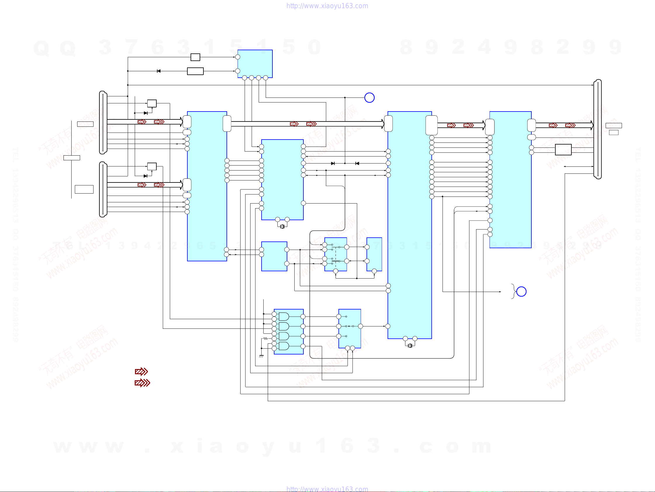
4-3. BLOCK DIAGRAM – HDMI SECTION –
3
77,76,
74,73,
71,70
67,68
64
63
62
58,57,
55,54,
52,51
49,48
46
45
44
9
Q1704
SW
Q1701-1703
BUFFER
B21,A21
SCL2
SDA2
HPD2
6
1
IC3503
SELECTOR
13
18
1,3,4,6,7,9
10,12
15
16
19
18
13
1,3,4,6,7,9
10,12
15
16
19
3
7
3.3V
9
D3511
D3512
Q3505
CLOCK +/-
Q3506
CLOCK +/-
4
6
D1701
SW
SCL
SDA
SW
SCL
SDA
2
2
Q
Q
DVD IN
3
CN3501
TEL 13942296513 QQ 376315150 892498299
HDMI
VIDEO 2 /
BD IN
CN3502
T
E
L
1
Y4,Z4
Y3,Z3
Y2,Z2
Y1,Z1
HPD_SINK
5
SCL_SINK
SDA_SINK
XOE
STR-K995
IC1907(3/3)
SYSTEM CONTROLLER
5
91
88
25,26,
28,29,
31,32,
34,35
S1
21
S2
22
S3
23
42
40
1
3
38
39
1
CE0
HDMI_S289HDMI_S12HDMI_RESET1HDMI_MUTE
90
TX
33
RX
34
TMDS_S1
51
TMDS_S2
52
TMDS_S3
53
TMDS_OEB
54
RX_HPDI
21
TX_RST
42
TX_INT
43
P5V_SELB
55
P5V_SELA
56
IC3507
DATA BUFFER
SCLA
SDAA
3
IC3519(2/2)
SUB CPU
XOUT
11 13
X3502
10MHz
SCLB
SDAB
5
RESET
RX_RST
RX_INT
EEPROMSEL1
XIN
72
6
MUTE
CSCL
CSDA
10
19
20
65
27
28
35
0
CSCL
CSDA
Q
1
2
BCK
LRCK
CSCL
5
RX
QE0 - QE23
1
VSYNC
ODCK
HSYNC
SCK
SD0
SD1
SD2
SD3
MCLK
SPDIF
9
124-121
117-114
111-108
105-99
96-92
1
119
DE
127
128
76
WS
75
74
73
72
71
79
70
5
8
3
C
EEPROM
6
5
IC3509
SCL
SDA
MAIN
SECTION
(Page 15)
7
WP
7
50,51,
54,55,
58,59,
62,63
89
91
67
40
39
6
RXC -/+
RX0 -/+
RX1 -/+
RX2 -/+
RESET
INT
MUTE
CSCL
CSDA
IC3511
3
HDMI_MUTE
D3502
IC3521
12
Q
14
1
5
10
D3501
13
3
0
4
49-58
61-65
67-70
75-79
66
80
12
11
10
43
44
42
18
17
2
1
9
8
7
6
5
8
D0 - D23
VSYNC
IDCK
DE
HSYNC
SCK
WS
SD0
SD1
SD2
SD3
MCLK
SPDIF
CSCL
CSDA
RESET
HPD
INT
9
IC3513
TX
9
TX0 +/TX1 +/TX2 +/-
TXC +/-
2
DSCL
DSDA
8
29,30,
32,33,
35,36
26,27
20
19
4
9
2
HDMI +5V
8
CLOCK +/-
Q3504
DATA
BUFFER
2
9
1,3,4,6,7,9
10,12
9
9
CN3504
13
HDMI
OUT
15
16
18
19
9
TEL 13942296513 QQ 376315150 892498299
w
w
w
• R-CH is omitted due to same as L-CH.
• Signal Path
: DIGITAL
: VIDEO
.
x
i
a
o
3.3V
y
42
DSDL
41
DSDA
IC3501
3
1
4
5
10
9
12
13
u
3
6
8
11
1
SELECTOR
2
4
5
6
IC3504
9 10
3 44
3
PWR5V
.
XTALOUT
84 85
28.322MHz
X3501
XTALIN
c
o
m
SPDIF
B
MAIN
SECTION
(Page 15)
STR-K995
1717
STR-K995
4-4. PRINTED WIRING BOARD – DIGITAL BOARD (SIDE A) –
Q
Q
12
3
7
6
• See page 14 for Circuit Boards Location.
3
345678
A
DIGITAL BOARD
TEL 13942296513 QQ 376315150 892498299
B
C
D
E
F
T
E
L
1
J1311
DMPORT
3
9
4
CL043
C1921
R1351
CL042
C1920
R1354
IC1302
D1302
2
2
R1356
C1361
W1000
FB1505
FB1504
CL044
C1911
IC1401
C1362
C1415
C1414
R1410
R1411
FB1350
R1301
FB1310
C1302
IC1303
9
R1357
R1358
CL045
CL046
L1403
C1404
C1401
C1409
C1408
JR1005
R1359
FB1453
R1327
C1301
R1303
C1304
C1303
JR1008
C1405
C1316
R1304
6
R1469
R1401
FB1405
R1407
1
FB1309
R1318
R1321
C1315
IC1301
R1308
R1307
R1306
5
R1319
R1360
JR1511
JR1020
R1305
R1556
R1502
IC1452
R1642
FB1452
C1002
R1309
1
D1301
C1522
FB1503
R1492
R1484
5
CNS506
R1312
R1313
R1325
R1310
FB1305
X1502
C1521
C1460
C1461
R1483
C1483
C1487
R1951
R1505
1
(SIDE A)
C1951
R1331
C1952
R1952
C1331
IC1017
R1311
X1301
R1501
C1509
C1511
3
R1511
R1512
R1523
R1513
R1504
R1506
R1507
IC1403
R1491
R1444
C1404
R1486
5
D
C1949
R1253
R1702
R1134
R1135
R1953
C1953
IC1502
RB1506 RB1504
R1516
R1508
C1443
R1446
RB1502RB1501
IC1501
C1472
C1471
IC1404
R1470
R1473
C1474
R1445
R1531
C1475
R1476
:Uses unleaded solder.
0
HDMI RE
BOARD
CN3512
(Page 38)
C1913
C1950
R1949
R1014
R1013
R1140
R1555
R1557
RB1500
RB1507
RB1503
RB1508
IC1111
1
R1574
R1573
IC1503
R1495
R1493
R1434
C1462
C1432
R1464
R1435
R1436
C1569
Q
R1570
R1571
R1572
R1541
R1514
C1502
R1510
IC1405
R1463
R1426
C1567
Q
R1150
R1143
R1144
R1160
R1161
C1704
C1706
R1494
R1466
R1424
C1422
R1425
C1424
C1568
5
4
C1701
R1703
R1709
R1711
R1120
R1704
R1012
R1701
IC1710
C1703
3
R1710
C1702
Q1703
R1707
R1713
E
E
Q1704
R1154
R1333
C1705
7
JW1700
R1714
E
Q1701
Q1702
D1701
R1705
R1716
E
R1151
R1121
R1076
IC1131
6
R1712
1
334
X1101
R1153
R1084
R1042
R1708
R1964
C1495
8
D1001
R1050
R1041
3
R1044
5
IC1700
IC1907
R1156
R1332
R1152
C1142
R1157
R1015
1
R1194
C1031
R1010
R1107
R1961
R1962
C1118
C1119
R1164
9
R1110
R1125
R1011
5
R1062
R1067
R1066
R1065
C1129
R1061
R1068
R1636
C1605
C1620
R1635
R1035
R1126
R1111
R1122
R1123
R1083
R1108
1
R1201
R1114
W1001
R1112
2
R1946
R1106
5
C1123
C1122
C1066
R1118
R1117
R1175
R1129
0
C1067
C1068
R1124
C1807
FB1308
R1077
4
1-872-697-
8
R1181
R1182
R1179
R1180
R1088
R1073
R1072
LP1000
9
9
2
14
(14)
8
4
2
• Semiconductor
Location
Ref. No.
D1001 C-6
D1301 D-3
D1302 C-3
D1701 D-6
IC1017 C-4
IC1111 D-5
IC1131 F-6
IC1301 C-3
IC1302 C-3
IC1303 D-3
IC1401 E-2
IC1403 E-4
IC1404 F-4
IC1405 F-5
IC1452 E-3
IC1501 D-4
IC1502 C-4
IC1503 E-5
2
8
9
IC1700 D-6
IC1710 D-6
IC1907 E-6
Q1701 D-6
Q1702 D-6
Q1703 D-6
Q1704 E-6
9
Location
9
9
9
TEL 13942296513 QQ 376315150 892498299
STR-K995
w
w
w
.
x
i
a
o
y
u
1
6
1818
3
.
c
o
m

STR-K995
4-5. PRINTED WIRING BOARD – DIGITAL BOARD (SIDE B) –
Q
Q
3
7
6
3
1
DIGITAL BOARD
• Semiconductor
Location
TEL 13942296513 QQ 376315150 892498299
Ref. No.
D1003 E-3
D1004 E-4
D1107 C-7
D1108 C-7
D1109 C-7
D1110 C-7
D1111 C-7
D1501 D-3
D1502 D-3
D1503 D-3
D1504 D-4
IC1001 F-3
IC1031 B-8
IC1351 C-2
IC1354 C-2
IC1901 B-7
IC1902 B-5
IC1904 C-6
IC1906 E-2
T
Location
E
L
MAIN
BOARD
CNP913
(Page 25)
1
3
DISPLAY
BOARD
CNS100
(Page 30)
for
FLASH
PROGRAMMING
U
H
9
4
2
IC1031
2
9
CL029
CL030
CL031
CL032
CNS504
JL1000
CL035
1
3
C1032
CNS511
6
CL028
CL034
CL033
R1105
R1078
C1905
C1908
R1186
• See page 14 for Circuit Boards Location.
5
1
5
(SIDE B)
HS1901
CL025
C1071
IC1901
CNP505
IC1904
C1985
CL022
5
R1192
C1140
R1039
R1187
R1184
R1183
R1185
C1171
R1191
C1172
C1149
1
C1906
D1109
C1144
R1188
C1145
C1131
D1108
C1100
CNP506
D1111
C1132
3
R1954
C1022
D1107
C1342
C1103
C1102
R1941
R1163
D1110
C1021
FB1101
R1947
R1948
C1079
CL021
JR1000
JR1010
C1146
R1159
C1970
C1667
1
3
C1124
C1141
C1604
C1971
C1661
C1121
C1139
CL037
C1255
C1961
R1093
CL036
CNS502
C1707
C1254
R1960
0
STANDBY
BOARD
CNP903
(Page 32)
C
JR1001
C1960
CL039
:Uses unleaded solder.
MAIN
BOARD
CNP912
(Page 25)
B
C1518
Q
IC1902
1
FB1502
FB1501
C1515
Q
C1517
R1644
C1423
C1458
3
C1525
C1516
JR1003
C1463
C1418
C1004
CL016
C1914
3
CL041
C1019
R1643
CL017
7
C1506
C1433
C1428
C1566
ANTENNA
FM
COAXIAL
6
C1513
C1508
C1507
C1505
R1645
C1547
TN1
AM
CNS507
C1520
C1519
JR1002
C1514
C1473
C1468
8
75
CL019
3
C1504
CL040
CNS501
C1510
1
C1503 C1501
CL020
R1641
JL001
9
CL018
R1260
R1261
C1987
5
C1481
C1442
IC1001
C1805
C1804
CL013
FB1302
D1504
D1004
C1491
C1448C1438
C1806
CL012
C1310
C1309
1
CL006
CL005
CL010 CL007
C1313
C1986
R1314
C1312
R1530
D1501
D1502
D1503
D1003
C1450
2
(Page 36)
CL004
CL008
CL009
CL011
R1323
5
C1455
C1001
3
1
3456789
VIDEO
BOARD
CNS206
A
CNS509
C1803
C2281
C1314
C1308
C1306
0
C1358
R1503
C1494
R1474
C1454
C1005
4
CL002
CL003
C1802
C1305
R1302
R1355
C1457
C1403
C1402
C1801
JR1009
JR1006
C1359
C1355
C1919
R1409
C1407C1406
DCDC
BOARD
CN4103
(Page 32)
E
CL001
CL023
C1800
8
R1637
C1910
9
CNP512
CL024
IC1354
3
C1354
R1096
1
IC1351
3
C1351
1
9
IC1906
R1353
1-872-697-
2
R1352
8
4
9
14
(14)
2
SAT IN
VIDEO 2/
BD IN
8
J1301
COAXIAL
DVD IN
OPTICAL
2
12
9
DIGITAL
9
9
9
A
B
TEL 13942296513 QQ 376315150 892498299
C
D
E
F
STR-K995
w
w
w
.
x
i
a
o
y
MAIN
BOARD
G
CN500
(Page 25)
u
1
6
3
1919
.
F
MAIN
BOARD
CNP501
(Page 25)
c
o
G
m
STR-K995
4-6. SCHEMATIC DIAGRAM – DIGITAL BOARD (1/5) –
• See page 41 for Waveform. • See page 42 for IC Block Diagram.
1 2 3 4 5 6 7 8 9 10 11 12 13
Q
Q
3
7
6
3
A
B
DIGITAL BOARD (1/5)
C
TEL 13942296513 QQ 376315150 892498299
R1354
9
C1361
R1356
0.1
470
R1358
470k
C1355
22
25V
2.6
8765
IC1303
TC7WU04FU(TE12R)
FB1504
0uH
C1362
0.01
IC1302
AUDIO IN SELECT
IC B/D
100
C1354
0.1
100R1351
0.1C1351
6
1.2
2.5
1.4
IC1303
T
E
D
E
G
H
K
F
L
I
J
DMPORT
OPTICAL
DIGITAL
COAXIAL
1
SAT
IN
VIDEO 2
BD IN
3
DVD
IN
P GND
VBUS +5V
CLINK_RX
CLINK_TX
CLINK_DET
DGND
CLINK_WM_DET
CLINK_WM_AD
AGND
AGND
CLINK_L
CLINK_R
WM_RXD
WM_TXD
VIDEO
VIDEO_GND
IC1354
OPTICAL IN
2
GND
0.1
1
OUT
VCC
TORX147L
GND
OUT
TORX147L
VCC
OPTICAL IN
W1001
CL043
CL042
CL044
CL045
CL046
2
3
2
1
3
R1355
C1921
FB1505
3.3
0.1
3.3
75
C1920
0.1
0.1
R1096
10k
1kR1352
1kR1353
2
0uH
IC1354
IC1351
IC1351
J1301
9
4
J1311
18P
1
2
3
NC
4
+5V
5
6
7
8
9
10
11
12
13
14
15
16
17
18
1
5
R1357
47k
1.2
4321
R1359
100
INVERTER
FB1350
0uH
1
5
C2281
10V
470
3.3
0
0.1
0.1
3
C1358
0.1
C1359
1000
6.3V
D1302
MA111-TX
0uH
FB1310
C1316
0.1
IC1302
TC74ACT153F(EL)
1
STROBE
B
1C3
1C2
5432
1C1
6
1C0
1Y
87
GND2 Y
C1987
0.1
1
VCC
STROBE
A
2C3
2C2
2C1
2C0
C1302
0.01
JR1005
R1303
33k
C1303
0.1
C1304
0.01
FB1302
0uH
0
R1304
16 15 14 13 12 11
10 9
R1327
100
R1301
5.6k
R1302
4.7k
3.3
3.3
100
C1301
5
0.1
0.1
2.5
0.1
3.3
2.9
2.9
2.9
3.3
C1305
C1306
0
CNS509
7P
FB1309
0uH
C1800
1000p
C1801
1000p
C1802
1000p
R1318
R1323
47
1.6
10k
46
CKSEL1
Q
BCK
1.6
22
R1306
D1301
MA111-TX
45
CKSEL0
DOSEL1
IC1301
LC89056W-E
LRCK
DATAO
1.6
100
R1308
C1314
0.1
3.3
43
44
DOSEL0
Q
DIGITAL AUDIO
I/F RECEIVER
IC B/D
IC1301
XSTATE
1.6
100R1309
10k
C1315
0.1
3.200
48
XMODE
DISEL
DOUT
DINO
DIN1
DIN2
DGND
DVDD
R_SDIN
987654321
VIN_AGND
10 11 12
LPF
AVDD
AGND
0.1
47
16V
CKOUT
1314151617181920212223
1.6
R1360
100
JR1020
0
V-SW4
DVDD
DGND
3.3
C1308
0.1
V-SW3
42
DGND
3
DVDD
0uHFB1305
41
1.6
0
R1319
A
V-SW2
40
MODEL1
XMCK
1.6
V-SW1
C1309
VIDEO BOARD
CNS206
(Page 37)
V MUTE
COMP-S2
COMP-S1
1234567
C1805
1000p
C1804
1000p
C1803
1000p
C1986
0.1
3.300
37
38
39
CE
CLK
XSEL
MODE0
3
BPSYNC
AUTO_VREF
F3/P3/C3_VF/DATA02
F2/P2/C2_F2/DLMP
F1/P1/C1_F1/FSB1
F0/P0/C0_F0/FSB0
CSFLAG
XOUT
XIN
EMPHA
AUDIO
24
0
1.6
R1325
R1311
0
1M
X1301
12.288MHz
C1310
18p
18p
C1331
0.1
C1952
0.01
R1952
10k
C1806
1000p
DI
DOUT
ERROR
7
DGND
DVDD
100R1311
JR1511
3.3
8
VCC
TC7WH157FK
A
IC1017
1
3.3
R1331
100
0R1321
252627282930313233343536
R1307
0uH
0
0
3.3
3.3
6
3.3
100
R1305
680
3.3
/G
B
R1951 10k
C1951 0.01
/A B
/Y
HDMI RE
8
BOARD
(1/2)
CN3512
D
(Page 39)
HDMI_CEC_IN
HDMI_RESET
HDMI_UART_RX
HDMI_UART_TX
HDMI_REG_CTL
1234567
R1314
10k
R1312
3
100
C1312
0.1
3.3
567
GND Y
432
HDMI_ERROR(MUTE)
100pC1313
1
R1953
10k
9
HDMI_SPDIF
CNS506
7P
R1332
100
5
C1953
0.01
1
IC1017
SELECTOR
2
CL013
CL011
CL010
CL008
CL007
CL006
CL005
CL004
CL003
CL002
CL001
5
No mark:FM
0
100R1313
4
4
18
5
6
7
9
10
11
12
13
14
15
16
17
19
20
21
22
23
24
25
26
27
28
29
30
31
32
34
55
33
39
40
3
2
35
8
2
8
4
9
DIGITAL
3
BOARD
(4/5)
(Page 23)
DIGITAL
4
BOARD
(5/5)
(Page 24)
9
DIGITAL
1
BOARD
(2/5)
(Page 21)
9
2
8
2
9
9
9
TEL 13942296513 QQ 376315150 892498299
9
STR-K995
w
L
w
w
.
x
i
a
o
2
DIGITAL
BOARD
(3/5)
(Page 22)
y
u
8983 84 85 86 87 88 90 91
1
6
2020
3
.
c
o
m

STR-K995
4-7. SCHEMATIC DIAGRAM – DIGITAL BOARD (2/5) –
• See page 41 for Waveform. • See page 47 for IC Pin Function Description.
1 2 3 4 5 6 7 8 9 10 11 12 13 14 15
Q
Q
3
7
6
3
1
A
B
CNS507
DIGITAL BOARD (2/5)
2
1
DIGITAL
BOARD
(1/5)
(Page 20)
3
33
35
39
40
R1949
47k
FB1501
C1949
0.1
R1253
0uH
C
TEL 13942296513 QQ 376315150 892498299
D
E
1k
R1260
1k
R1261
C1517
C1518
0.1
470
10V
F
C1510
C1503
0.1
27p
C1521
1M
R1512
6
0.1
C1511
0.1
0.1C1501
220R1523
10kR1513
T
E
L
G
1
H
37
38
41
3
9
4
2
2
X1502
13.9MHz
FB1503
0uH
R1511
C1522
100R1504
100R1505
100R1506
100R1507
9
10k
27p
100R1502
220R1503
42
I
J
5
DIGITAL
BOARD
(3/5)
(Page 22)
43
44
45
46
47
48
49
50
K
L
51
M
52
w
w
w
N
.
x
i
9P
CL020
C1950
220p
10k
5
1101112131415161718192021222324252627282930
3.3
2.6
1.8
98765432
2.6
1.6
0
1.7
1.7
3.3
1.6
1.8
1.6
1.6
1.7
1.7
1.7
1.7
1.7
1.6
1.6
1.6
a
TN1
5
ANTENNA
AM
75
FM
COAXIAL
SDCEDI
CLK
DO
CL019
JL001
100
R1501
C1516
0.1
C1515
470
10V
0.1C1509
2.6
118
119
120
TST3
VDDI
1
3
VSS
XRST
EXTIN
LRCKI3
VDDI
BCKI3
PLOCK
VSS
1
MCLK1
VDDI
VSS
MCLK2
MS
SCKOUT
LRCKI1
VDDE
BCKI1
SDI1
LRCK0
BCK0
VSS
KFSI0
SD01
SD02
SD03
SD04
SPDIF
LRCKI2
BCKI2
SDI2
VSS
HACN
3132333435363738394041424344454647484950515253545556575859
1.4
3.2
100R1508
o
GND
R1516
GP11
HDIN
1
L_CH
VCC
R_CH
123456789
C1019
0.1
CL018
CL017
FB1502
0uH
RB1506
C1514
0.1
10k
2.7
3.2
0.2
112
113
114
115
116
117
A0PMSDI3
SDI4
SYNC
TST2
HCLK
HDOUT
HCS
GP12
GP13
GP14
3.2
3.3
3.3
3.3
C1504
0.1
100R1531
y
5
0.2
110
0.200
109
VSS
RB1501
107
108
IC1501
AUDIO DSP
IC1501
CXD9718BQ
GP15
CE0
3.3
3.2
100
3.300
106
D1D0A2A1VSS
CS0
3.2
WEO
100
111
VDDI
2.6
u
3.302.600
104
105
VDDE
VMDI
3.3
3.3
103
102
VSS
3.3
0
100
RB1502
C1513
0.1
100
101
VSS
D5D4D3D2VDDE
VMDO
PAGE2
CL016
Q
VSS
PAGE1
C1505
0.1
1
PAGE0
63
64
65
66
67
68
69
70
71
72
73
9
74
75
76
77
78
79
80
81
82
6
DIGITAL
BOARD
(4/5)
(Page 23)
7
DIGITAL
BOARD
(5/5)
(Page 24)
2
8
2
9
9
9
TEL 13942296513 QQ 376315150 892498299
9
32 31 30 29 28 27
VSS
VDD
VSS
D11
D10
13 14 15 16 17 18 19
3.3
0.1
0.1
0
432
1.5
0
1
m
4
D0D1D2D3VDD
D9
D8
0.1
0.1
3.3
C1519
C1520
0.1
2
SRAM
No mark:FM
8
4
9
0.2
0.2
0.2
0.2
23
26 25 24
A6A0A1
A2
GNDGND
A11
A10
WE
A8
A7
22
20 21
0.2
0.2
0.2
0.2
0.1
9
8
IC1502
2
+9V REG
00003.30000
37 36
35 34 33
D4D5D6
D7
BLL
BHL
IC1502
IS61WV6416BLL-12TLI
D15
D14
D13
CS
8101112
3.2
0.1
0.1
0.1
5
567
GNDY
S
ST
8
VCC
IC1503
TC7WH157FU(TE12R)
IC1503
SELECTOR
D12
0.1
Y
B
A
A13
0.3
1
3
o
1
C1913
0.47
0.2
44 43 42 41 40 39 38
A5
A9
0.2
1
RB1503
100
RB1508
100
RB1507
100
RB1500
100
c
9
IC1902
0.2
0.2
3.2
OEA7A6
A12
A15
A14
34567 9
1
2
0.2
0.3
0.3
5
100R1514
R1510
1.6
100
C1502
0.1
3.3
8
IC1902
TA7809S
16.3 9
O
I
3
G
6
0.1C1508
R1555
220
.
3
2
R1557
220
C1914
47
16V
100
RB1504
0
0.2
0.2
0.2
0.2
0.2
919293949596979899
VSS
BOOT
Q
TST1
1.3
BST
MOD1
3.2
6
MOD0
3.3
A8A7A6A5A4A3D7D6VDDI
EXLOCK
2.6
D8/GP0
D9/GP1
D10/GP2
D11/GP3
D12/GP4
D13/GP5
D14/GP6
D15/GP7
VDDI
60
C1506
XTRST
VDDE
GP10
0.1
3.3
90
3
TDI
TCK
TMS
TD0
A10
A11
A12
A9
VSS
VSS
VDDI
GP8
GP9
A13
A14
A15
A16
A17
6162636465666768697071727374757677787980818283848586878889
VSS
220R1541
10kR1574
7
10kR1573
3.3
10kR1572
3.3
3.3
10kR1571
10kR1570
3.3
0.2
0.2
0.2
0.2
0.2
0.2
0.2
0.2
3.3
0.1
0.1
0.1
0.1
2.6
C1507
0.1
0
0
0.2
0.2
0.2
C1525
470
10V
3
STR-K995
2121

STR-K995
4-8. SCHEMATIC DIAGRAM – DIGITAL BOARD (3/5) –
• See page 42, 43 for IC Block Diagrams.
1 2 3 4 5 6 7 8 9 10 11 12 13 14 15
7
2
DIGITAL
BOARD
(1/5)
(Page 20)
6
3
87 8884 908983 86 9185
A
Q
Q
3
DIGITAL BOARD (3/5)
B
TEL 13942296513 QQ 376315150 892498299
C
R1401
D
100
E
IC1401
T
E
L
1
AD CONVERTER
IC B/D
3
9
4
SYSCLK
2
C1403
10
50V
2
DOUT
9
BCK
6
F
C1404
1.6
3.3
1.4
DGND
BYPASS
R1409
IO
3.2
C1002
0
0.47
DOUT
FSYNC
7
1.7
1.7
10987654321
LRCK BCK
C1483
680p
C1481
330p
G
H
0.1
47
16V
FB1405
C1001
470
10V
0uH
SCK
VDD
AGND
PDWN
C1409
3.2
IC1001
TA7805S
5
3 1
0.1
0.01
+5V REG
IC1001
G
2
20 19 18 17 16 15 14 13 12 11
OSR
FMT0
FMT1
MODE0
MODE1
IC1401
PCM1803DBR
LIN
RIN
V REF 1
V REF 2
VCC
C1401
2.6
0.1
C1408
50V10C1407
4.9
0.1
C1405
5
C1402
50V10C1406
2.6
2.6
CNS501
B TO B
15P
15
C LINK L
14
GND
13
C LINK R
12
T.L OUT
11
GND
10
T.R OUT
9
F
MAIN
BOARD
I
(1/4)
CNP501
(Page 26)
L IN
GND
R IN
R OUT
L OUT
SW OUT
MAIN AGND
C OUT
8
7
6
CL040
5
+7V
4
3
CL041
2
1
0.01C1415
0.01
C1414
470R1411
470R1410
J
K
w
w
w
.
x
i
1
LRCK
5
R1483
6.8k
C1448
10
50V
R1486
1k
C1487
2200p
C1547
2200p
a
5
C1450
0.1
C1455
10
50V
FB1452
FB1453
1
3
1SS367-T3SONY
D1004
1SS367-T3SONY
0.1
5
0.1
6
0.1
7
7
0R1484
8
IC1403
NJM4565M(TE2)
R1446
1k
o
0uH
0uH
C1457
C1454
0.1
C1004
0.1
D1003
FR_OUT
IC1403
AMP
C1438
10
50V
1
R1474
10k
C1494
0.1
10
50V
C1005
4
3
2
1
0.1
-7
0
0
0
y
R1469
100
3.3
2.3
1.6
1.6
3.3
1.3
1.3
1.3
37
38
39
40
41
42
43
44
45
46
47
48
R1444
6.8k
R1445
C1442
330p
FL_OUT
0
5
3.3
RST(A_LOW)
SCKI
SCKO
BCK
LRCK
TEST
VDD
DGND
DATA1
DATA2
DATA3
ZEROA
0
3.300
3233343536
ML
MC
MDI
MDO
ZERO7(1602_NC)
ZERO8(1602_NC)
DATA4(1602_NC)
IC1452
AUDIO CODEC
IC B/D
IC1452
PCM1602APT
Q
ZERO1
ZERO3
ZERO4
ZERO5
ZERO2
R1642
R1641 10k R1645 10k
R1407
ZERO6NCNC
54321
C1460
10k
100
0.1
SW_OUT
IC1404
C1474
0.1
R1473
8.2k
C1468
50V
R1476
1k
10
0.1
2.6
2.6
7
R1436
1k
1
5
6
7
8
NJM4565M(TE2)
C1441
680p
u
C1473
C1566
2200p
C1569
2200p
0.1
5
28293031
ND
Q
9876
2.6
6.8k
R1492
AMP
IC1404
C1428
27 26 25
VCC1
AGND1
VOUT8(1602_NC)
VOUT7(1602_NC)
VOUT6
VOUT5
10 11 12
2.6
2.6
C1461
6.8kR1491
10
50V
6
5
0.1
8.2kR1470
VCC2
VOUT4
2.6
6.8kR1495
4
3
2
1
AGND2
AGND3
AGND4
AGND6
AGND5
VOUT1
VOUT2
VOUT3
C1471
C_OUT
VCC3
VCC4
VCC5
VCOM
0.1
-7
0
0
0
3
24
23
22
21
20
19
18
17
16
15
14
13
C1472
0.1
R1434
C1567
2200p
C1568
2200p
3
6.8kR1494
6.8k
R1435
C1433
330p
5
5
5
2.6
2.6
2.6
7
0
6.8kR1493
C1491
50V
C1475
0.1
R1643
10k
R1644
10k
C1432
680p
5
DIGITAL
BOARD
(2/5)
9
8
2
8
G
MAIN
BOARD
(1/4)
CN500
(Page 26)
2
9
9
9
TEL 13942296513 QQ 376315150 892498299
9
0
R1424
6.8k
R1425
0
C1423
330p
m
4
C1422
680p
No mark:FM
8
9
9
CNS502
B TO B
CL037
CL036
CL039
11P
2
1
NC
NC
2
3
NC
VOL_IC_CLK
4
vOL_IC_DATA_LAT
5
vAVS_CTRL
6
7
SBR_OUT
SBL_OUT
8
SR_OUT
9
-7V
10
SL_OUT
11
37
38
41
42
43
44
45
46
47
48
49
50
51
52
4
53
54
56
57
58
59
60
61
62
8
(Page 21)
DIGITAL
BOARD
(5/5)
(Page 24)
100R1556
0JR1008
1SS367-T3SONY
R1530
100k
1
2
5
D1501
1
SR_OUT
9
D1502
D1503
D1504
1SS367-T3SONY
1SS367-T3SONY
1SS367-T3SONY
5
8
10
3
6
SL_OUT
IC1405
5
6
7
8
NJM4565M(TE2)
c
AMP
IC1405
4
3
2
1
C1458
10
50V
R1466
1k
o
-7
0.1
0.1
0.1
C1462
680p
C1463
330p
.
R1463
6.8k
C1418
10
50V
R1426
1k
0.1
0.1
0.1
7
0R1464
STR-K995
2222
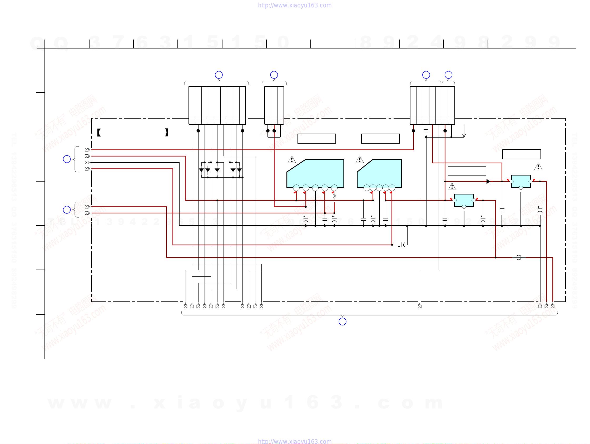
4-9. SCHEMATIC DIAGRAM – DIGITAL BOARD (4/5) –
STR-K995
Q
1 2 3 4 5 6 7 8 9 10 11 12
Q
3
7
6
3
1
A
B
CNP506
9P
TEL 13942296513 QQ 376315150 892498299
63
64
C
D
T
DIGITAL
BOARD
(2/5)
(Page 21)
DIGITAL
BOARD
E
(1/5)
(Page 20)
6
65
66
4
3
18
L
DIGITAL BOARD (4/5)
1
3
9
4
2
2
9
6
5
SUB_T
9
CL022
5
FRONT_B_RY
B'ABLE_RY
7
8
D1109
D1108
MA111-TX
MA111-TX
1
1
MAIN BOARD
(4/4)
CNP913
U E C B
(Page 29)
FRONT-RY
C/REAR/SB-RY
HP_CTRL
HP_RY
WOOFER_RY
2
3
4
5
6
D1111
3
MA111-TX
D1107
MA111-TX
PROTECTOR
1
CL021
D1110
MA111-TX
5
GND
1
CL024
0
DCDC BOARD
(Page 33)
+6.5V
2
CL023
CN4103
GND
3
CNP512
Q
3P
8
IC1906 IC1901
+5V REG
IC1906
IC SI-3050KM-TL
VC
VIN
GND
VOUT
SENSE
1
2345
3.3
6.3
Q
C1919
22
35V
5
3
C1911
0.1
5
C1910
100
10V
R1637
7
0
6
12345
3
C1985
0.1
+3.3V REG
IC1901
SI-3004KWF
3.3
1
C1906
470
10V
9
7.6
5
C1905
0.1
2.6
1
CNP505
7P
2
STANDBY
BOARD
CNP903
(Page 33)
+R2 (+15V)
1
CL025
5
0
STOP
2
C1071 0.1
4
STBY GND
+9V(STBY)
3
4
PW RY
5
CL012
8
9
MAIN BOARD
CNP912
(Page 29)
+R4
R4 GND
6
7
BA50BC0FP-E2
7.6
1
C1031
0.47
9
(4/4)
W1000
IC1031
+5V REG
IC1031
3
VCC
OUT
GND
2
C1032
470
10V
2
8
D1001
1SR154-400TE-25
5
9
4
2
9
IC1904
+3.3V REG
IC1904
BA33BC0FP-E2
6.8 3.3
VCC
1
C1021
0.47
2
8
GND
3
OUT
2
C1022
470
10V
9
9
TEL 13942296513 QQ 376315150 892498299
9
E
F
G
C1908
470
10V
FB1308
0uH
No mark:FM
92 93 94 95 96 97 98 99 100 101 102 103 104 105 106
9
DIGITAL
BOARD
(5/5)
(Page 24)
STR-K995
w
w
w
.
x
i
a
o
y
u
1
6
3
2323
.
c
o
m
 Loading...