

Sony STRK-6800-P Service manual
STR-DE597P/K6800P
SERVICE MANUAL
Ver 1.0 2004. 06
• STR-DE597P/K6800P are
the FM/AM receiver section
in HT-DDW860/6800DP.
Manufactured under license from Dolby Laboratories.
“Dolby”, “Pro Logic” and the double-D symbol are
trademarks of Dolby Laboratories.
“DTS”, “DTS-ES”, “Neo:6” are trademarks of Digital
Theater Systems, Inc.
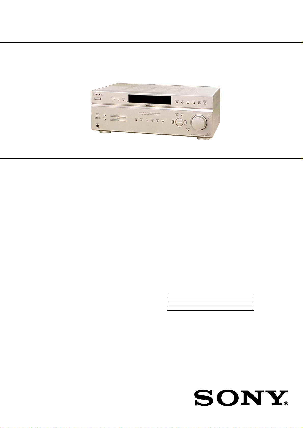
Photo: STR-K6800P
SPECIFICATIONS
US Model
STR-K6800P
AEP Model
UK Model
Australian Model
STR-DE597P
AUDIO POWER SPECIFICATIONS
POWER OUTPUT AND TOTAL HARMONIC
DISTORTION:
(Models of area code US only)
With 8 ohm loads, both channels driven, from
120 – 20,000 Hz; rated 90 watts per channel
minimum RMS power, with no more than
0.7 % total harmonic distortion from 250
milliwatts to rated output.
Amplifier section
Power Output
Models of area code US
(8 ohms 1 kHz, THD 10 %)
Models of area code AEP, UK
(8 ohms 1 kHz, THD 0.7 %)
(8 ohms 1 kHz, THD 10 %)
1)
2)
FRONT
: 120 W/ch
2)
CENTER
SURR
SURR BACK
FRONT
CENTER
SURR
SURR BACK
FRONT
CENTER
SURR
SURR BACK
: 120 W
2)
: 120 W/ch
2)
: 100 W/ch
2)
: 100 W
2)
: 100 W/ch
2)
: 120 W/ch
2)
: 120 W
2)
: 120 W/ch
2)
: 120 W
2)
: 100 W
2)
: 120 W
Models of area code AUS
(8 ohms 120 Hz – 20 kHz, THD 0.09 %)
(8 ohms 1 kHz, THD 0.7 %)
(8 ohms 1 kHz, THD 10 %)
1) Measured under the following conditions:
Area code Power requirements
US 120 V AC, 60 Hz
AEP, UK 230 V AC, 50 Hz
AUS 240 V AC, 50 Hz
2) Depending on the sound field settings and the
source, there may be no sound output.
2)
FRONT
: 80 W/ch
2)
CENTER
2)
SURR
: 80 W/ch
SURR BACK
2)
FRONT
: 100 W/ch
2)
CENTER
2)
SURR
: 100 W/ch
SURR BACK
2)
FRONT
: 120 W/ch
2)
CENTER
2)
SURR
: 120 W/ch
SURR BACK
: 80 W
2)
: 80 W
: 100 W
2)
: 100 W
: 120 W
2)
: 120 W
– Continued on next page –
9-879-028-01
2004F04-1
© 2004. 06
FM STEREO/FM-AM RECEIVER
Sony Corporation
Home Audio Company
Published by Sony Engineering Corporation
1

STR-DE597P/K6800P
Inputs (Analog)
MULTI CH IN, SA-CD/ Sensitivity: 800 mV
CD, MD/TAPE, DVD, Impedance: 50 kiloohms
VIDEO 1, 2
Inputs (Digital)
DVD (Coaxial) Sensitivity: –
VIDEO 2, SA-CD/CD Sensitivity: –
(Optical) Impedance: –
Outputs (Analog)
MD/TAPE (OUT), Voltage: 800 mV
VIDEO 1 (AUDIO OUT) Impedance: 10 kiloohms
SUB WOOFER V oltage: 2 V
Reproduction frequency range:
Tone
Gain levels ±6 dB, 1 dB step
Impedance: 75 ohms
Impedance: 1 kiloohms
28 – 20,000 Hz
FM tuner section
Tuning range 87.5 – 108.0 MHz
Antenna FM wire antenna
Antenna terminals 75 ohms, unbalanced
Intermediate frequency 10.7 MHz
AM tuner section
Tuning range
Models of area code US
With 10-kHz tuning scale: 530 – 1,710 kHz
With 9-kHz tuning scale: 531 – 1,710 kHz
Models of area code AEP, UK, AUS
With 9-kHz tuning scale: 531 – 1,602 kHz
Antenna Loop antenna
Intermediate frequency 450 kHz
3) You can change the AM tuning scale to 9 kHz or 10 kHz.
After tuning in any AM station, turn off the recei ver . While
holding down PRESET TUNING + or TUNING +, press
?/1. All preset stations will be erased when you change
the tuning scale. To reset the scale to 10 kHz (or 9 kHz),
repeat the procedure.
3)
3)
Video section
Inputs/Outputs
Video: 1 Vp-p, 75 ohms
COMPONENT VIDEO:
(Except for models of area code AEP, UK)
Y: 1 Vp-p, 75 ohms
PB/CB/B-Y: 0.7 Vp-p,
75 ohms
PR/CR/R-Y: 0.7 Vp-p,
75 ohms
80 MHz HD Pass Through
General
Power requirements
Area code Power requirements
US 120 V AC, 60 Hz
AEP, UK 230 V AC, 50/60 Hz
AUS 240 V AC, 50 Hz
Power consumption 220 W
Power consumption (during standby mode)
0.3 W
Dimensions (w/h/d) (Approx.)
430 × 157.5 × 312 mm
(16 7/8 × 6 2/8 × 12 2/8
inches) including
projecting parts and
controls
Mass (Approx.) 8.0 kg (17 lb 11 oz)
Design and specifications are subject to change
without notice.
•Abbreviation
AUS: Australian model
2
STR-DE597P/K6800P
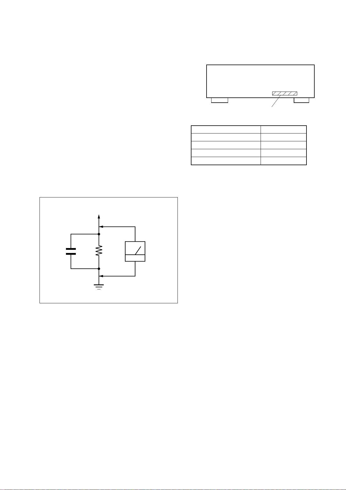
SAFETY CHECK-OUT
After correcting the original service problem, perform the following safety check before releasing the set to the customer:
Check the antenna terminals, metal trim, “metallized” knobs, screws,
and all other exposed metal parts for AC leakage.
Check leakage as described below.
LEAKAGE TEST
The AC leakage from any exposed metal part to earth ground and
from all exposed metal parts to any exposed metal part having a
return to chassis, must not exceed 0.5 mA (500 microampers.).
Leakage current can be measured by any one of three methods.
1. A commercial leakage tester, such as the Simpson 229 or RCA
WT-540A. Follow the manufacturers’ instructions to use these
instruments.
2. A battery-operated AC milliammeter. The Data Precision 245
digital multimeter is suitable for this job.
3. Measuring the voltage drop across a resistor by means of a
VOM or battery-operated AC voltmeter. The “limit” indication is 0.75 V, so analog meters must have an accurate lowvoltage scale. The Simpson 250 and Sanwa SH-63Trd are examples of a passive VOM that is suitable. Nearly all battery
operated digital multimeters that have a 2 V AC range are suitable. (See Fig. A)
To Exposed Metal
Parts on Set
MODEL IDENTIFICATION
— BACK PANEL —
Part No.
MODEL PART No.
STR-K6800P: US 4-254-238-0s
STR-DE597P: AEP 4-254-238-1s
STR-DE597P: UK 4-254-238-2s
STR-DE597P: AUS 4-254-238-3s
•Abbreviation
AUS: Australian model
0.15 µF
1.5 k
Ω
Earth Ground
AC
voltmeter
(0.75 V)
Fig. A. Using an AC voltmeter to check AC leakage.
SAFETY-RELATED COMPONENT WARNING!!
COMPONENTS IDENTIFIED BY MARK 0 OR DOTTED LINE
WITH MARK 0 ON THE SCHEMATIC DIAGRAMS AND IN
THE PARTS LIST ARE CRITICAL TO SAFE OPERATION.
REPLACE THESE COMPONENTS WITH SONY P ARTS WHOSE
PART NUMBERS APPEAR AS SHOWN IN THIS MANUAL OR
IN SUPPLEMENTS PUBLISHED BY SONY.
3

STR-DE597P/K6800P
TABLE OF CONTENTS
1. GENERAL
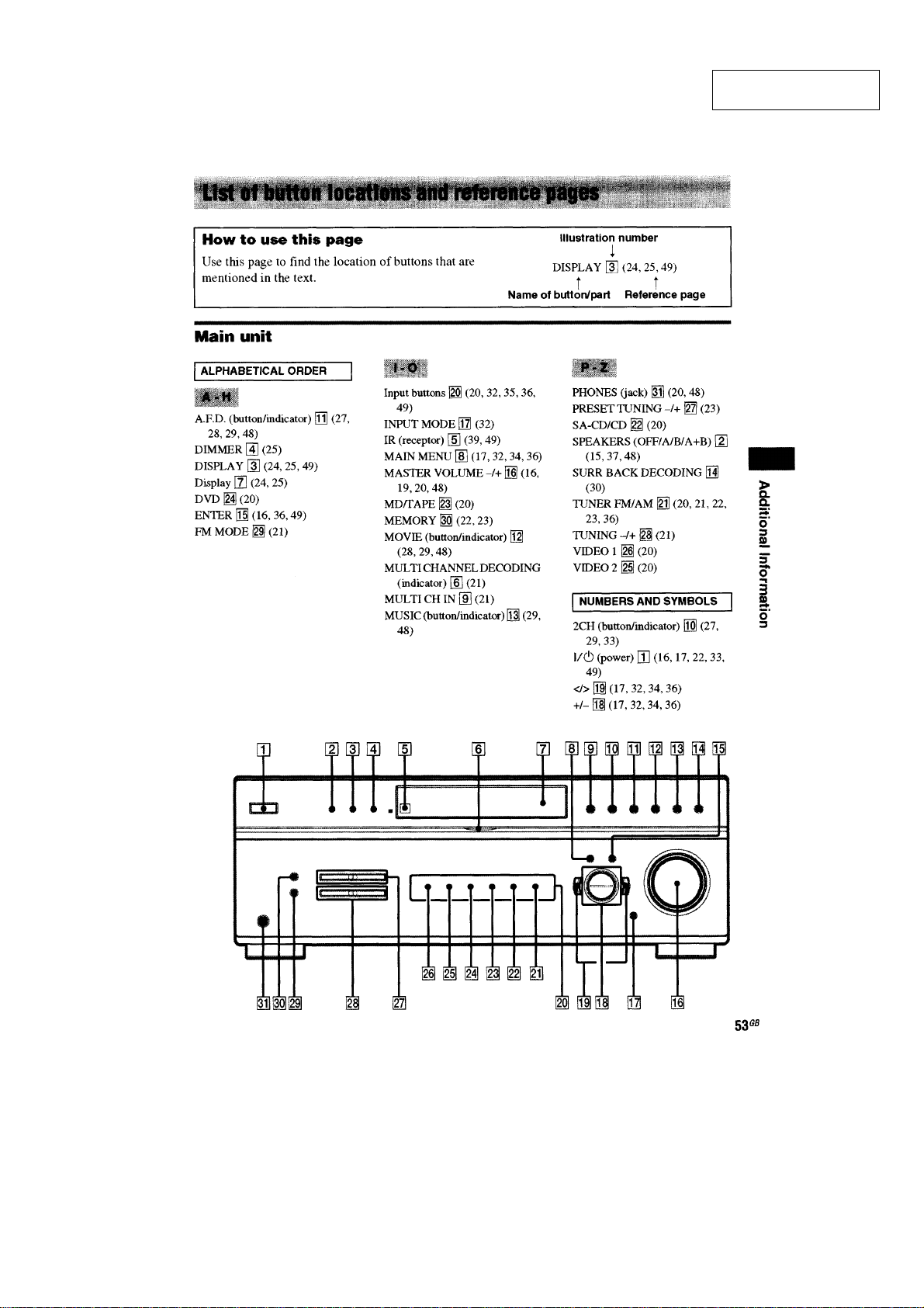
Main unit ................................................................................. 5
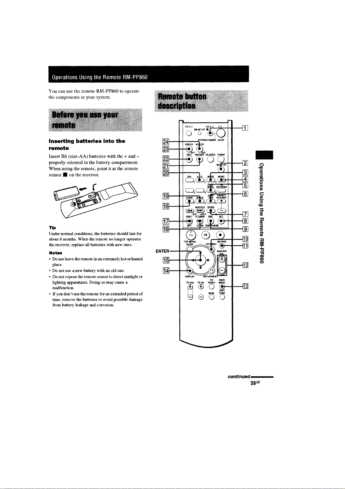
Remote button description....................................................... 6
2. DISASSEMBL Y
2-1. Case .....................................................................................7
2-2. Front Panel Section ............................................................. 8
2-3. Back Panel Section.............................................................. 8
2-4. Digital Board ....................................................................... 9
2-5. Standby Board ..................................................................... 9
2-6. Main Board ....................................................................... 10
2-7. SB AMP Board.................................................................. 10
3. TEST MODE ..................................................................... 11
4. DIAGRAMS
4-1. Circuit Boards Location .................................................... 12
4-2. Block Diagram – Tuner/Audio Section – .......................... 13
4-3. Block Diagram – Digital Section – ................................... 14
4-4. Block Diagram – Video Section – ..................................... 15
4-5. Block Diagram – Key/Display Section – .......................... 16
4-6. Block Diagram – Power Section – .................................... 17
4-7. Printed Wiring Boards – Main Section – .......................... 19
4-8. Schematic Diagram – Main Section (1/2) – ...................... 20
4-9. Schematic Diagram – Main Section (2/2) – ...................... 21
4-10. Printed Wiring Board – Digital Section (1/2) – ................ 22
4-11. Printed Wiring Board – Digital Section (2/2) – ................ 23
4-12. Schematic Diagram – Digital Section (1/3) – ................... 24
4-13. Schematic Diagram – Digital Section (2/3) – ................... 25
4-14. Schematic Diagram – Digital Section (3/3) – ................... 26
4-15. Printed Wiring Boards –
Center/Surround Back Speaker Section – ......................... 27
4-16. Schematic Diagram –
Center/Surround Back Speaker Section – ......................... 28
4-17. Printed Wiring Board – Video Section –........................... 29
4-18. Schematic Diagram – Video Section –.............................. 30
4-19. Printed Wiring Boards – Display Section – ...................... 31
4-20. Schematic Diagram – Display Section –........................... 32
4-21. Printed Wiring Boards – Power Section –......................... 33
4-22. Schematic Diagram – Power Section – ............................. 34
4-23. IC Block Diagrams............................................................ 35
5. EXPLODED VIEWS
5-1. Case Section ...................................................................... 42
5-2. Front Panel Section ...........................................................43
5-3. Back Panel Section............................................................ 44
5-4. Chassis Section ................................................................. 45
6. ELECTRICAL PARTS LIST ........................................ 46
4
SECTION 1
GENERAL
STR-DE597P/K6800P
This section is extracted
from instruction manual.
5
STR-DE597P/K6800P
6
SECTION 2
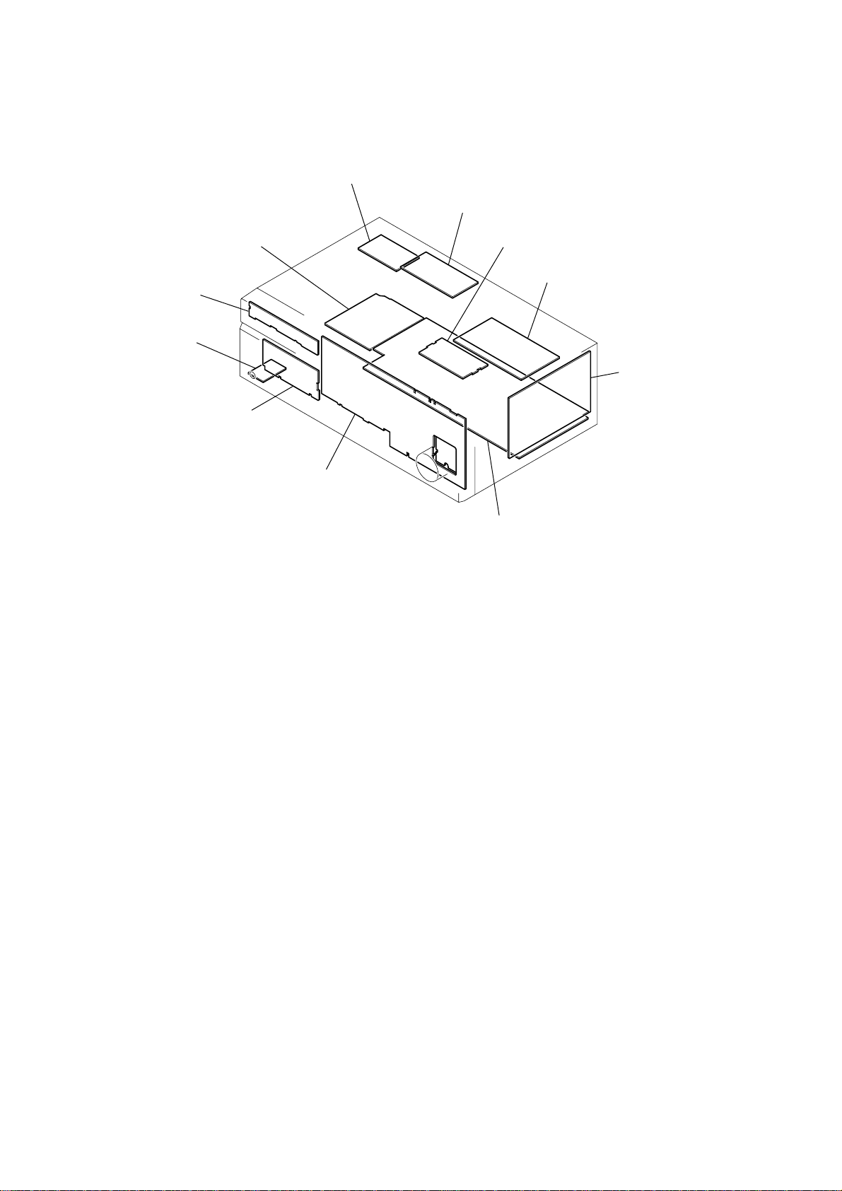
DISASSEMBLY
Note : This set can be disassemble according to the following sequence.
SET
2-1. CASE
(Page 7)
STR-DE597P/K6800P
2-2. FRONT PANEL SECTION
(Page 8)
2-5. STANDBY BOARD
(Page 9)
2-3. BACK PANEL SECTION
(Page 8)
2-4. DIGITAL BOARD
(Page 9)
2-6. MAIN BOARD
(Page 10)
Note : Follow the disassembly procedure in the numerical order given.
2-1. CASE
1
two screws
(case 3 TP2)
2-7. SB AMP BOARD
(Page 10)
2
two screws
(case 3 TP2)
3
two screws
(case 3 TP2)
4
case
7
STR-DE597P/K6800P
)
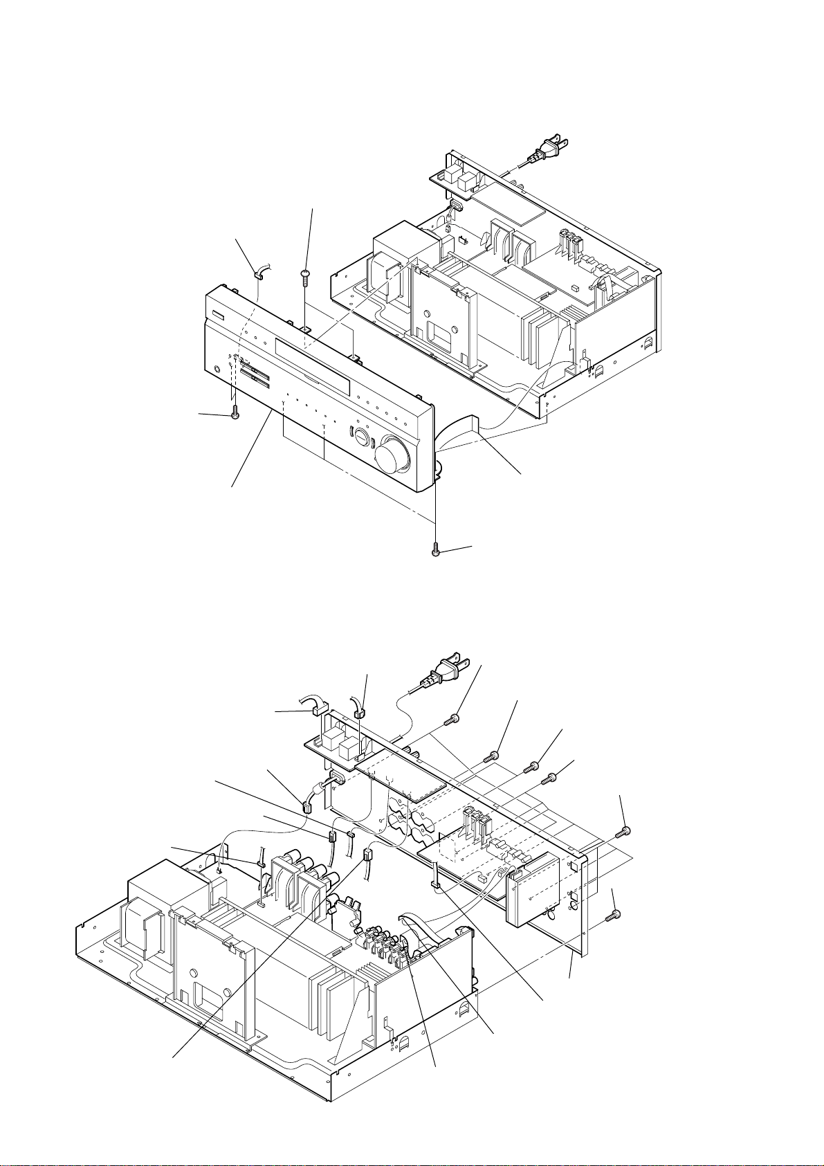
2-2. FRONT P ANEL SECTION
4
two screws
(+BVTP 3 x 8)
2
CNP791
3
two screws
(+BVTP 3 x 8)
2-3. BACK PANEL SECTION
5
CNP502
6
7
CNP913
6
front panel section
9
CN908
0
CNP901
CNP501
8
CN906
5
three screws
(+BVTP 3 x 8)
qa
three screws
(+BVTP 3 x 8)
qd
(+BVTP 3 x 8)
1
CNS505
screw
qf
two screws
(+BVTP 3 x 8)
qg
seven screws
(+BVTP 3 x 8)
qh
three screws
(+BVTP 3 x 8
qs
screws
(+BVTP 3 x 8)
qj
back panel section
3
CNP203
1
CNS250
4
CNP503
2
connector
8
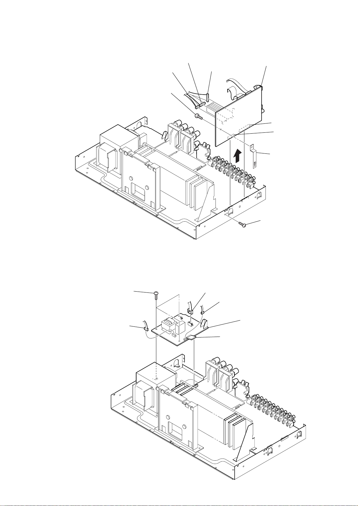
2-4. DIGIT AL BOARD
3
8
screw
(+BVTP 3 x 8)
CNP507
2
CNP510
1
CNP506
5
STR-DE597P/K6800P
0
DIGITAL board
7
CNP501
CNP500
6
9
bracket (digital)
2-5. ST ANDBY BOARD
5
three screws
(+BV SUMITITE (B3))
4
CNP903
3
CNP902
2
CNP804
1
CNP915
4
screw
(+BVTP 3 x 8)
6
STANDBY board
9
STR-DE597P/K6800P
s
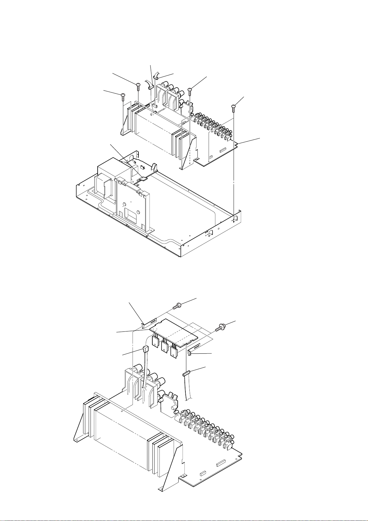
2-6. MAIN BOARD
6
screw
(+BV SUMITITE (B3))
4
two screws
(+BV SUMITITE (B3))
1
CNP915
3
CNP802
2
CNP912
5
two screws
(+BV SUMITITE (B3))
7
two screws
(+BV SUMITITE (B3))
8
MAIN board
2-7. SB AMP BOARD
7
SB AMP board
1
CN572
5
bracket (SUR)
4
two screws
(+BVTP 3 x 8)
6
bracket (SUR)
2
CN574
3
three screw
(transistor)
10
SECTION 3
TEST MODE
STR-DE597P/K6800P
FACTORY PRESET MODE
* All preset contents are reset to the default setting.
* Procedure:
While depressing the [FM MODE] and the [DISPLAY] buttons
simultaneously, press the
?/1 button to turn on the main power .
The message “FA CT OR Y” appears for a moment and the present
contents are reset to the default values.
AM CHANNEL STEP 9 kHz/10 kHz SELECTION
MODE (US model only)
* Either the 9 kHz step or 10 kHz step can be selected for the AM
channel step.
* Procedure:
Press the [TUNER FM/AM] button to set AM and press the ?/1
button to turn off the main power.
While depressing the [PRESET TUNING +] button or the
[TUNING +] button, press the ?/1 button to turn on the main
power.
Either the message “9k STEP” or “10k STEP” appears for a
moment and select the desired step.
SPEAKER SIZE SELECTION MODE
* Either the normal speaker or micro satellite speaker can be se-
lected.
* Procedure:
While depressing the [DIMMER] button, press the ?/1 button to
turn on the main power.
Either the message “NORM. SP .” or “MICRO SP.” appears for a
moment and select the desired speaker size.
VACUUM FLUORESCENT DISPLAY TEST MODE
* All fluorescent segments are tested.
When this test is activated, all segments light on at the same
time, then each segment lights on one after another.
* Procedure:
While depressing the [TUNING ---] and the [SPEAKERS $OFF/A/
B/A+B%] buttons simultaneously , press the
the main power.
1. ALL segments light on.
SP A
D
D
LFE
SW
CR
L
SL S SR
SBL SB SBR
D
SP B SLEEP OPT COAX MULTI CH IN 96/24
D
DIGITALEX PRO LOGIC II x DTS-ES NEO:6 MPEG-2 AAC RDS
[2CH], [A.F.D.], [MOVIE], [MUSIC] and [MULTI CHANNEL DECODING] LED light on.
2. Press the [VIDEO 1] button, confirm display.
SP A
D
D
LFE
LSWR
S
SB
D
SP B SLEEP OPT COAX MULTI CH IN 96/24
D
DIGITALEX PRO LOGIC II x DTS-ES NEO:6 MPEG-2 AAC RDS
[A.F.D.] and [MUSIC] LED light on.
?/1 button to turn on
MEMORY
kHz
mft.
MHz
kHz
mft.
MHz
DIRECT
dB
MEMORY
DIRECT
dB
D.RANGE EQ STEREO MONO
D.RANGE EQ STEREO MONO
4. Press the [VIDEO 1] button, all segments and all LEDs light off.
5. Every pressing the [VIDEO 1] button turns on each segment and
LED one after another in the same order.
(Not only the [VIDEO 1] button, b ut also the other b uttons such
as [VIDEO 2], [DVD], [MD/TAPE], [SA-CD/CD] and [TUNER FM/
AM] can be used.)
SOUND FIELD CLEAR MODE
* The preset sound field is cleared when this mode is activated.
Use this mode before returning the product to clients upon
completion of repair.
* Procedure:
While depressing the [2CH] button, press the ?/1 button to turn
on the main power.
The message “SF. CLR.” appears for a moment and initialization is performed.
SOFTWARE VERSION DISPLAY MODE
* The software version is displayed.
* Procedure:
While depressing the [TUNING ---] and the [DISPLAY] buttons
simultaneously, press the ?/1 button to turn on the main po wer .
The model name, destination and the software version are displayed for a moment.
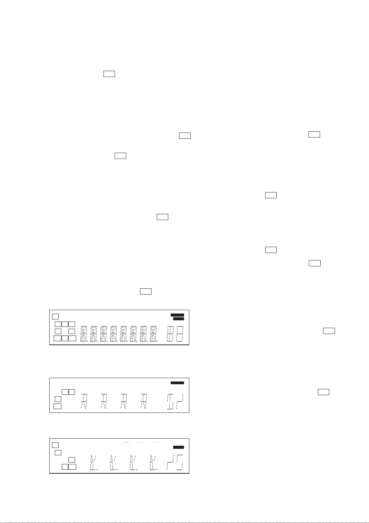
KEY CHECK MODE
* Button check
* Procedure:
While depressing the [TUNING ---] and the [MAIN MENU] buttons
simultaneously, press the ?/1 button to turn on the main po wer .
Either the message “REST 28” appears.
Every pressing of any button other than the
?/1 counts down
the buttons. The buttons which are already counted once are not
counted again. When all buttons are pr essed “REST 00” appears.
AUTOBETICAL MODE (AEP, UK model only)
* When this mode is used, the receiver scans the broadcasts that
can be received by the tuner, and sets up the broadcasts.
Be sure to start scanning after connecting the antenna.
* Procedure:
Check that the antenna is connected.
While depressing the [MEMORY] button, press the ?/1 button
to turn on the main power.
The message “AUTO-BETICAL SELECT” appears for a moment and the receiver starts scanning.
COMMAND MODE SELECTION MODE
* The command mode (AV1 or AV2) of the remote commander
can be selected.
* Procedure:
While depressing the [ENTER] button, press the ?/1 button to
turn on the main power.
Either the message “C.MODE.AV 1” or “C.MODE.AV 2” appears for a moment and select the desired mode.
3. Press the [VIDEO 1] button, confirm display.
SP A
D
D
D
DIGITALEX PRO LOGIC II x DTS-ES NEO:6 MPEG-2 AAC RDS
D.RANGE EQ STEREO MONO
kHz
mft.
MHz
C
SL SR
SBL SBR
D
SP B SLEEP OPT COAX MULTI CH IN 96/24
[2CH], [MOVIE] and [MULTI CHANNEL DECODING] LED light
on.
MEMORY
DIRECT
11
STR-DE597P/K6800P
4-1. CIRCUIT BOARDS LOCATION
SECTION 4
DIAGRAMS
BRIDGEABLE board
SPEAKER board
POWER board
HEADPHONE board
TUNING board
STANDBY board
SB AMP board
VIDEO board
DIGITAL board
DISPLAY board
MAIN board
12
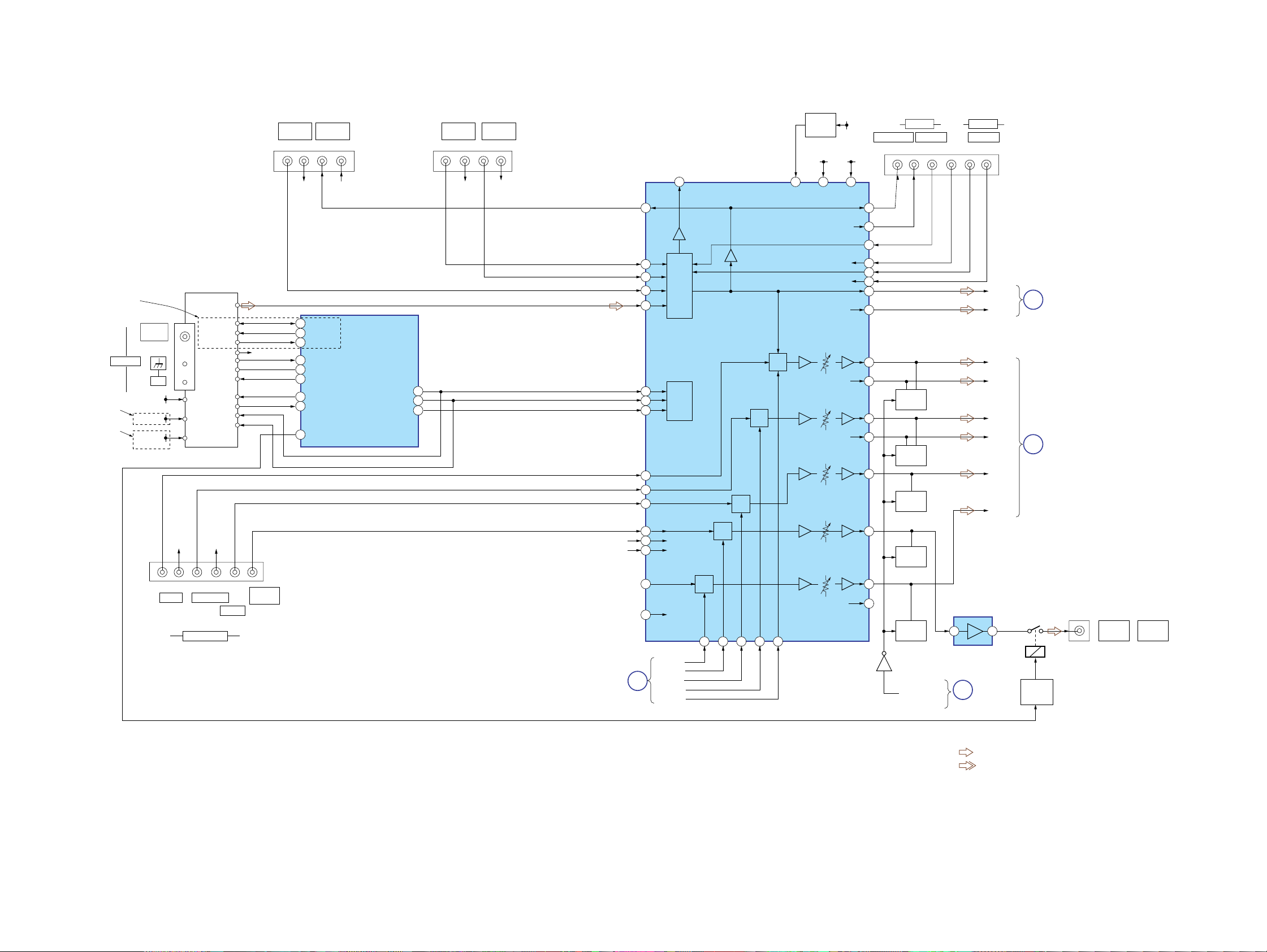
4-2. BLOCK DIAGRAM — TUNER/AUDIO SECTION —
STR-DE597P/K6800P
DE597P:
AEP,UK MODEL
DE597P:
AEP,UK MODEL
DE597P:AUS/
K6800P
ANTENNA
TN1
FM/AM TUNER UNIT
FM 75Ω
COAXIAL
AM
TU+10V
TU+3.3V
3.3V
(STBY)
J401
-1 -2 -3 -4 -5 -6
LR
FRONT
RDS DATA
RDS INT
FM SIG OUT
MUTING
R-CH
LR
SURROUND
MULTI CH IN
L-CH
R-CH
STEREO
TUNED
DATA
CLOCK
R-CH
CENTER
3.3V
SA-CD/CDINMD/TAPE
L
J402 J403 J404
R-CH
CE
DO
SUB
WOOFER
R
53
52
43
76
75
78
74
73
70
LR
R-CH
RDS DATA
RDS CLK
RDS SIG
STEREO
TUNED
MUTE
S LATCH
DO
SW RY
OUT
R-CH
IC.DATA
IC.CLK
VOL LATCH
SYSTEM
CONTROL
IC1101 (1/4)
MD/TAPEINDVD AUDIO
LRLR
-1 -2 -3 -4-1 -2 -3 -4
16
17
22
R-CH
IN
DIR
FUNCTION SELECT
SW
SEL
IC401
C
SEL
SEL
L
SEL
SL
R-CH
R-CH
R-CH
DIGITAL
SECTION
(Page 14)
61
4
72
74
SEL
SW
76
80
18
MCU
20
I/F
19
57
54
55
56
53
R-CH
58
R-CH
52
51
SBL OUT
SW OUT
C OUT
C
SL OUT
L OUT
SBL
SEL
R-CH
15 11 12 13 10
REG
Q471
21 24 22
DVDD
R-CH
R-CH
R-CH
R-CH
R-CH
R-CH
R-CH
+7V
+7V-7V
AVCCAVEE
63
62
68
67
70
69
6
7
46
47
40
41
35
34
28
29
Q379
VIDEO 1
AUDIO OUT AUDIO INAUDIO IN
L
RL
-3 -4 -5 -6
MUTE
Q300,310
MUTE
Q320,330
MUTE
Q350
MUTE
Q340
MUTE
Q360
SYSTEM MUTE
VIDEO 2
RLR
-1 -2
L-CH
R-CH
FL-CH
FR-CH
SL-CH
SR-CH
C-CH
SB-CH
5 7
SUB WOOFER
AMP
IC402
DIGITAL
B
SECTION
(Page 14)
A
D
RELAY
DRIVER
Q560
DIGITAL
SECTION
(Page 14)
POWER
SECTION
(Page 17)
J309
RY560
AUDIO
OUT
SUB
WOOFER
STR-DE597P/K6800P
• Signal path
: TUNER (FM/AM)
: VIDEO (AUDIO)
• R-ch is omitted due to
same as L-ch.
• Abbreviation
AUS: Australian model
13 13
STR-DE597P/K6800P
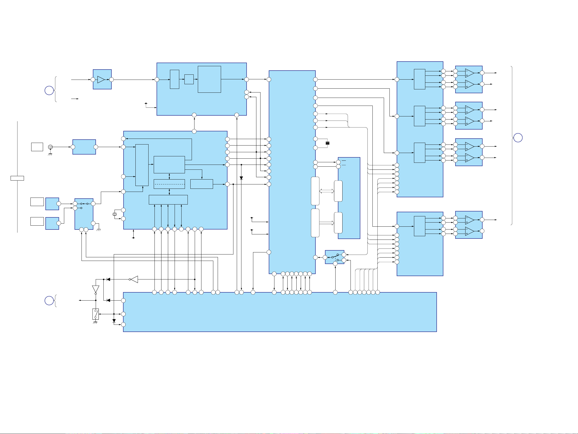
4-3. BLOCK DIAGRAM — DIGITAL SECTION —
DIGITAL
TUNER/
AUDIO
SECTION
(Page 13)
DVD
IN
(COAXIAL)
SA-CD/CD
IN
(OPTICAL)
VIDEO 2
IN
(OPTICAL)
A
J1301
IC1354
IC1351
OUT
OUT
A/D
CONVERTER
AMP
IC1402
L-IN
R-IN
1
1
3 7
5
R-CH
IC1303
WAVE
SHAPER
SELECTOR
IC1302
AB
14 2
3 1
23
X1301
12.288MHz
8
D1105
DIGITAL AUDIO
I/F RECEIVER
DOUT
2
DIN2
5
DIN1
4
DIN0
3
21
XOUT
22
XIN
+3.3V
Q1105
+5V-2
IC1301
INPUT
VDD
INV.
AINL
2
A.5V
CLKCEDIDOBPSYNC
38 37 36 35 33 47 17
ADC
DATA
DEMODULATOR
Pa,Pb DETECTION LOCK
C bit DETECTION
MICROPROCESSOR
I/F
IC1401
SDTO
9 18
LRCK
10
SCLK
12
PDN
13
24
13 22
14 29
15 28
16 30
D1301
34 59
+2.5V
VDDI
+3.3V
VDDE
SDI1 SD01
GP8
69
KFSI0
BCKI2
LRCKI2
SDI2
LRCKI1
15
BCKI1
17
EXLOCK
37
GP12
GP9
68
MCLK
11
20
XMCK
DETECTION
XSTATE
48
AUDIO
XMODE
I/F
AUDIO
CKOUT
BCK
LRCK
DATAO
ERROR
LPF
CKSEL1
NC
HCS
HACN
2 11336 35 33 3432
DSP
IC1501
XRST
PM
SD02
SD03
SD04
SCKOUT
LRCKO
BCKO
MCLK1
MCLK2
CSO
WEO
BST
HDIN
HDOUT
D0-15A0-15
HCLK
23
24
25
26
14
19
20
9
12
44
45
108,107,105 -102,99,
112,110,109,97 - 92,
56
X1502
13.5MHz
98,80 - 77,75 - 72
85-82,66 - 64
SWITCH
IC1503
5
6
MCLK
LRCKO
BCKO
SDRAM
IC1502
CS
6
17
WE
D0-15A0-15
16-13,10 - 7
29 - 32,35 - 38,
1 - 5,18 - 21
24 - 27,42 - 44,
LRCKO
2
1
MCLK
LRCKO
BCKO
CSN-1
PDN-1
CLK
CDTI
MCLK
LRCKO
BCKO
CSN-2
PDN-2
CLK
CDTI
SDTI3
8
SDTI1
6
SDTI2
7
MCLK
4
LRCK
9
BICK
5
10
CSN
3
PDN
CCLK
11
CDTI
12
SDTI
3
MCLK
1
LRCK
4
BICK
2
CSN
6
PDN
5
CLK
7
DTI
8
6CH DAC
IC1452
DAC
DAC
DAC
2CH DAC
IC1451
DAC
LOUT3LOUT3+
ROUT3ROUT3+
LOUT1LOUT1+
ROUT1ROUT1+
LOUT2LOUT2+
ROUT2ROUT2+
OUTLOUTL+
OUTROUTR+
AMP
IC1403
2
17
3
18
6
15
5
16
AMP
IC1405
2
25
3
26
6
23
5
24
AMP
IC1404
2
21
3
22
6
19
5
20
AMP
IC1406
2
11
3
12
6
9
5
10
1
7
1
7
L OUT
R-CH
SL OUT
R-CH
TUNER/
C
AUDIO
1
7
1
7
C OUT
SW OUT
SBL OUT
SECTION
(Page 13)
TUNER/
AUDIO
SECTION
B
SYSTEM MUTE
(Page 13)
STR-DE597P/K6800P
Q1103
INV.
Q1104
GATE
D1106
D1103
SYSTEM_MUTE
24
99
ERROR
25
ANA/DIG
95 96 97 98
DIR DI
DIR CE
DIR_CLK
DIR DO
94
DIR CKSEL1
93100
DIR_XMODE
DIR_XSTATE
90
91
SELECT1
SELECT2
9
DIR_DATAO
AK5380-PDN
8
GP12
21
GP9
HCS1
6 74 18 19 205
XRST1
HACN1
PM1
HDIN
HDOUT
HCLK
92
BST SEL
SYSTEM
CONTROL
IC1101 (2/4)
CSN-1
3
BST
AK4355_CSN
AK4381_CSN
AK4355_PDN
211513121410
AK4355_CLK
AK4381_PDN
AK4355_CDTI
• R-ch is omitted due to
same as L-ch.
CDTI
CLK
PDN-2
PDN-1
CSN-2
1414
4-4. BLOCK DIAGRAM — VIDEO SECTION —
J301 (1/2)
12
13
5
3
2
1
SELECTOR
13
5
3
COMPONENT
VIDEO
VIDEO 2
IN
DVD
IN
VIDEO 1
VIDEO
DVD
P
P
P
P
R/CR/
R/CR/
B/CB/
B/CB/
-1
VIDEO
IN
-2
VIDEO
IN
-1
VIDEO
IN
Y
B-Y
R-Y
Y
B-Y
R-Y
J201 (1/2)
J200 (1/2)
-4
-5
-6
-1
-2
-3
COMPONENT VIDEO SELECTOR
0X
1X
0Z
1Z
0Y
1Y
VIDEO
IC203
V1
V2
DVD
IC301
BCA
10 9 11
XCOM
ZCOM
YCOM
INH
STR-DE597P/K6800P
DE597P:AUS/K6800P
VIDEO AMP
IC302
6dB AMP
Q301
INV.
VIN2
3
6dB AMP
VIN3
5
6dB AMP
VIN1
1
6dB AMP
6dB AMP
14
4
15
6
75Ω
DRIVER
75Ω
DRIVER
75Ω
DRIVER
75Ω
DRIVER
75Ω
DRIVER
VOUT2
VOUT3
VOUT1
V1.OUT
M.OUT
VCC
+5V-3
11
9
13
VEE
-5V-3
V-SW4
V-SW3
VCC
+5V-3
15
1
+5V-3
-5V-3
J301 (2/2)
-7
-8
-9
IC807
+5V
3 1
REG
IC804
-5V
3 2
REG
Y
P
P
B/CB/
R/CR/
B-Y
R-Y
MONITOR
OUT
+15V
-15V
COMPONENT
VIDEO
J200 (2/2)
J201 (2/2)
-3
VIDEO
OUT
-2
VIDEO
OUT
VIDEO 1
MONITOR
• Signal path
: VIDEO
• Abbreviation
AUS: Australian model
V3
9
NC
7
VEE
SW2
SW3
SW4
V-SW4
SW1
V-SW1
OR
D203,204
10 6 14 2
4
V-SW2
V-SW3
SW5
-5V-3
V-SW1
V-SW2
V-SW3
V-SW4
V SW1
V SW2
V SW3
V SW4
KEY/DISPLAY
E
SECTION
(Page 16)
STR-DE597P/K6800P
15 15
STR-DE597P/K6800P
4-5. BLOCK DIAGRAM — KEY/DISPLAY SECTION —
VIDEO
SECTION
(Page 15)
V SW1
V SW2
E
V SW3
V SW4
FLASH
PROGRAMMING
CNP503
1
2
7
6
5
EEPROM
IC1131
SDA
SCL
S152
I
/
I
FLASH1
FLASH2
MD2
MD0
RESET
SIRCS
FL DISPLAY DRIVER
IC100
STB
9
DIN
7
CLK
8
OUT
1
1
3
SEG1
I
SEG16
GRID12
I
GRID1
SW1
SW2
SW3
SW4
REMOTE
CONTROL
RECEIVER
IC102
RV102
MASTER
VOLUME
14
I
29
31
I
42
1
2
3
4
FL101
VACUUM
FLUORESCENT
DISPLAY
D102-105
SW1
86
SW2
87
SW3
88
SW4
89
83
X1101
16MHz
5
6
X1
X0
82
SDA
34
SCL
33
56
POWER KEY
28
FLASH1
27
FLASH2
MD2
51
MD0
49
SYSTEM
CONTROL
IC1101 (3/4)
VOL ENC A
VOL ENC B
BLUE LED
FL LAT
FL DATA
FL CLK
SIRCS
57
59
60
54
45
46
47
9
4
2
LED DRIVE
Q100
BUFFER
IC101
8
6
3
D101
+3.3V
(STBY)
IC1111
RESET
A/D0
A/D1
A/D2
38
39
40
12
77
RSTX
SW NETWORK
S130,132,134,136-141
SW NETWORK
S120-128
SW NETWORK
S100,101,103,105,107,109-113
STR-DE597P/K6800P
1616
4-6. BLOCK DIAGRAM — POWER SECTION —
PRE DRIVER
IC701
IN 2
PRE
FL-CH
FR-CH
R-CH
8
DRIVE
DRIVE
+VOUT2
-VOUT2
-B-1 +B
STR-DE597P/K6800P
J791
PHONES
R-CH
12
11
POWER AMP
Q701-704
R-CH
CURRENT
DETECT
Q705,706
R-CH
OVERLOAD
DETECT
D740,Q740
R-CH
RELAY
DRIVER
Q790
RELAY
DRIVER
Q611
RY791
RY602
R-CH
TM602
L
FRONT B
R
TM601
TUNER/
AUDIO
SECTION
(Page 13)
D
SL-CH
SR-CH R-CH
C-CH
SB-CH
PROTECTOR
FRONT RY
HP DETECT
SYSTEM
CONTROL
IC1101 (4/4)
BRIDGEABLE RY
P0WER RY
HP_RY
REAR_RY
C RY
SP_B_RY
61
62
66
69
68
55
67
72
58
8
1
1
D1107
D1108
IN 2
IN+
IN +
D1111
PRE
DRIVE
PRE
DRIVE
PRE
DRIVE
PRE DRIVER
IC601
DRIVE
PRE DRIVER
IC501
DRIVE
PRE DRIVER
IC571
DRIVE
D721,722,732
Q722,723,725
D1110
HP-RY
FRONTRY
REAR-RY
CENTER-RY
HP DETECT
SB-RY
-B-1 +B
-B-1 +B
-B-1 +B
PROTECTOR
+VOUT2
-VOUT2
+VOUT
-VOUT
+VOUT
-VOUT
12
11
6
5
6
5
IC691
OVERLOAD
DETECT AMP
-B-1
-B SWITCH
Q691,692
72
POWER AMP
Q651-654
POWER AMP
Q501-504
POWER AMP
Q572-574
R-CH
CURRENT
DETECT
Q655,656
R-CH R-CH
OVERLOAD
DETECT
D640,Q640
RELAY
DRIVER
Q710
RELAY
DRIVER
Q610
RELAY
DRIVER
Q550
RY601
RY501
RY701
R-CH
R-CH
TM501
L
FRONT A
R
L
SURROUND
R
CENTER
SPEAKERS
IMPEDANCE
USE 8-16Ω
• Signal path
: TUNER (FM/AM)
• R-ch is omitted due to
CURRENT
DETECT
Q505,506
CURRENT
DETECT
Q575
+B
-B
IC1904
+3.3V
REG
-32V REG
Q801
IC1071
+3.3V
REG
13
13
-32V
TU+10V
TU+3.3V
+7V
-7V
+5V-2
+5V-1
+2.5V
+3.3V
+3.3V
(STBY)
5
2
OVERLOAD
D540,Q540
OVERLOAD
D575,Q577
IC1001
+5V
REG
IC1901
BACK-UP
SWITCH
DETECT
DETECT
DE597P:
AEP,UK MODEL
13
4
HP-RY
IC1902
+10V
REG
IC801
+7V
REG
-7V
REG
IC802
IC1031
+5V
REG
SB-RY
FRONT RY
REAR-RY
13
31
23
13
CENTER-RY
HP DETECT
+15V
-15V
RECT
D802
RELAY
DRIVER
Q809
D920-923
D805-808
RELAY
DRIVER
Q901
RECT
RECT
-32V
RECT
D910-913
F1
F2
RELAY
SWITCH
RY801
RY901
D804
TRANSFORMER
R810
R811
R910
TRANSFORMER
SURROUND
BACK
T901
POWER
T902
POWER
same as L-ch.
F901
STR-DE597P/K6800P
STOP
Q921
48
D914
D915
~
AC IN
17 17
STR-DE597P/K6800P
THIS NOTE IS COMMON FOR PRINTED WIRING
BOARDS AND SCHEMATIC DIAGRAMS.
(In addition to this, the necessary note is
printed in each block.)
for schematic diagram:
• All capacitors are in µF unless otherwise noted. (p: pF)
50 WV or less are not indicated except for electrolytics
and tantalums.
• All resistors are in Ω and 1/
specified.
f
•
• 2 : nonflammable resistor.
• 5 : fusible resistor.
• C : panel designation.
Note: The components identified by mark 0 or dotted line
• A : B+ Line.
• B : B– Line.
•Voltage and waveforms are dc with respect to ground
•Voltages are taken with a VOM (Input impedance 10 MΩ).
•Waveforms are taken with a oscilloscope.
• Circled numbers refer to waveforms.
• Signal path.
• Abbreviation
: internal component.
with mark 0 are critical for safety.
Replace only with part number specified.
under no-signal (detuned) conditions.
no mark : FM
Voltage variations may be noted due to normal production tolerances.
Voltage variations may be noted due to normal production tolerances.
F : TUNER (FM/AM)
L : VIDEO (AUDIO)
I : VIDEO
J : CD (ANALOG)
c : CD (DIGITAL)
AUS : Australian model.
4
W or less unless otherwise
for printed wiring boards:
• X : parts extracted from the component side.
f
•
• : Pattern from the side which enables seeing.
Caution:
Pattern face side: Parts on the pattern face side seen from the
(Side B) pattern face are indicated.
Parts face side: Parts on the parts face side seen from the
(Side A) parts face are indicated.
• Abbreviation
: internal component.
AUS : Australian model.
C
Q
B
E
Q
BCE
Q
B
C
These are omitted.
These are omitted.
E
• Waveforms (DIGITAL Board)
1V/DIV 50nsec/DIV
1
3.8Vp-p
12.288MHz
IC1301
1V/DIV 0.2µsec/DIV
2
IC1301
1V/DIV 50nsec/DIV
3
IC1301
1V/DIV 50nsec/DIV
4
IC1501
1V/DIV 50nsec/DIV
5
IC1501
1V/DIV 50nsec/DIV
6
(CKOUT)
qd
3.07MHz
(BCK)
qf
12.288MHz
(XOUT)
wa
13.5MHz
(MCLK1)
9
13.5MHz
(MCLK2)
qs
3.2Vp-p
3.5Vp-p
2.2Vp-p
3.5Vp-p
IC1501
1V/DIV 50nsec/DIV
7
IC1101
12.288MHz
(SCKOUT)
qf
16MHz
id
3.8Vp-p
2.1Vp-p
(X1)
STR-DE597P/K6800P
1818
 Loading...