Sony STRDA-4300-ES Service manual

STR-DA4300ES
SERVICE MANUAL
Ver. 1.1 2007.10
This receiver incorporates Dolby* Digital and Pro Logic Surround and the DTS** Digital Surround System.
*Manufactured under license from Dolby Laboratories.
Dolby, Pro Logic, Surround EX, and the double-D symbol are trademarks of Dolby Laboratories.
** Manufactured under license from DTS, Inc.
“DTS”, “DTS-ES” and “Neo:6” are registered trademarks of DTS, Inc. and “DTS-HD Master Audio”,
“DTS-HD High Resolution Audio” and “DTS 96/24” are trademarks of DTS, Inc.
SPECIFICATIONS
US Model
Canadian Model
AUDIO POWER SPECIFICATIONS
(US model)
POWER OUTPUT AND TOTAL
HARMONIC DISTORTION:
With 8 ohm loads , both channe ls dri v e n, from
20 − 20,000 Hz; rated 100 watts per channel
minimum RMS power, with no more than 0.09%
total harmonic distortion from 250 milliwatts to
rated output.
Amplifier section
POWER OUTPUT
Rated Power Output at Stereo Mode
(8 ohms 20 Hz − 20 kHz,
THD 0.09%): 100W + 100W
Reference Power Output a t Stereo Mode
(4 ohms 20 Hz − 20 kHz,
THD 0.15%): 85W + 85W
Reference Power Output
(8 ohms 1 kHz, THD 0.7%)
FRONT
CENTER
SURROUND
SUR BACK
1) 2)
2)
: 110W + 110W
2)
: 110 W
2)
: 110W + 110W
2)
: 110W + 110W
Reference Power Output
1)
Depending on the sound field settings and the source,
there may be no sound output.
2)
Measured under the following conditions:
Power requirements: 120 V AC, 60 Hz
Frequency response
PHONO RIAA equalization curve
MULTI CHANNEL
INPUT, SA-CD/CD,
MD/TAPE, DVD/BD,
TV, SAT/CATV,
VIDEO 1/2/3
Inputs (Analog)
PHONO Sensitivity: 2.5 mV
MULTI CHANNEL
INPUT, SA-CD/CD,
MD/TAPE, DVD/BD,
TV, SAT/CATV,
VIDEO 1/2/3
(4 ohms 1 kHz, THD 0.7%)
2)
: 100W + 100W
FRONT
2)
CENTER
SURROUND
SUR BACK
: 100 W
2)
: 100W + 100W
2)
: 100W + 100W
± 0.5 dB
10 Hz − 100 kHz
± 3 dB
Impedance: 50 kohms
S/N: 90dB (A, 20 kHz
LPF)
Sensitivity: 150 mV
Impedance: 50 kohms
S/N: 100 dB (A, 20 kHz
LPF)
Inputs (Digital)
DVD/BD,VIDEO 2,
SA-CD/CD (Coaxial)
VIDEO 1, VIDEO 3,
SAT/CATV, TV, MD/
TAPE (Optical)
Outputs
MD/TAPE (REC OUT),
VIDEO 1 (AUDIO OUT)
FRONT L/R, CENTER,
SURROUND L/R,
SUR BACK L/R , SUB
WOOFER
EQUALIZER
Gain levels ±10 dB, 1 dB step
FM tuner section
Tuning range 87.5 − 108.0 MHz
Antenna (aerial) FM wire antenna (aerial)
Antenna (aerial) terminals
Impedance: 75 ohms
S/N: 96 dB (A, 20 kHz
LPF)
S/N: 96 dB
(A, 20 kHz LPF)
Voltage:150 mV
Impedance: 1 kohm
Voltage: 2 V
Impedance: 1 kohm
75 ohms, unbalanced
– Continued on next page –
9-887-785-02
2007J05-1
© 2007.10
MULTI CHANNEL AV RECEIVER
Sony Corporation
Home Audio Division
Published by Sony Techno Create Corporation

STR-DA4300ES
AM tuner section
Tuning range
With 10-kHz tuning scale
With 9-kHz tuning scale
Antenna (aerial) Loop antenna (aerial)
3)
You can change the AM tuning scale to either 9 kHz
or 10 kHz. After tuning in any AM station, turn off
the receiver. While holding down TUNING MODE,
press POWER on the receiver. All preset stations will
be erased when you change the tuning scale. To reset
the scale to 10 kHz (or 9 kHz), repeat the procedure.
530 − 1,710 kHz
531 − 1,710 kHz
3)
3)
Video section
Inputs/Outputs
Video: 1 Vp-p, 75 ohms
COMPONENT VIDEO:
Y: 1 Vp-p , 75 ohms
P
: 0.7 Vp-p, 75 ohms
B/CB
P
: 0.7 Vp-p, 75 ohms
R/CR
80 MHz HD Pass Through
HDMI Video
Input/Output (HDMI Repeater block)
640 × 480p@60Hz
720 × 480p@59.94/60Hz
1440 × 480p@59.94/60Hz (pixel sent 2times)
1280 × 720p@59.94/60Hz
1920 × 1080i@59.94/60Hz
1920 × 1080p@59.94/60Hz
720 × 576p@50Hz
1440 × 576p@50Hz (pixel sent 2times)
1280 × 720p@50Hz
1920 × 1080i@50Hz
1920 × 1080p@50Hz
1920 × 1080p@24Hz
General
Power requirements 120 V AC, 60 Hz
Power output (DIGITAL MEDIA PORT)
DC OUT: 5 V, 7 0 0 m A
Power consumption 350 W/480 VA (US/Canada)
Power consumption (duri ng standby mode)
0.7 W (when “HDMI
Control” and “RS-232C
Control” are set to “OFF”)
Dimensions 430 × 175 × 430 mm
(width/height/depth)
including projecting parts and
controls
Mass (Approx.) 14.5 kg
Supplied accessories
Operating Instructions
Quick Setup Guide (1)
HDMI CONTROL Guide (1)
GUI Menu List (1)
Optimizer microphone ECM-AC2 (1)
FM wire antenna (aerial) (1)
AM loop antenna (aerial) (1 )
AC power cord (mains lead) (1)
Remote commander RM-AAL011 (1)
Remote commander RM-AAU018 (1)
R6 (size-AA) batteries (4)
Design and specifications are subject to change
without notice.
2
STR-DA4300ES
r
Notes on chip component replacement
• Never reuse a disconnected chip component.
• Notice that the minus side of a tantalum capacitor may be
damaged by heat.
SAFETY CHECK-OUT
After correcting the original service problem, perform the following
safety check before releasing the set to the customer:
Check the antenna terminals, metal trim, “metallized” knobs, screws,
and all other exposed metal parts for AC leakage.
Check leakage as described below.
LEAKAGE TEST
The AC leakage from any exposed metal part to earth ground and
from all exposed metal parts to any exposed metal part having a
return to chassis, must not exceed 0.5 mA (500 microamperes.).
Leakage current can be measured by any one of three methods.
1. A commercial leakage tester, such as the Simpson 229 or RCA
WT -540A. Follow the man ufacturers’ instructions to use these
instruments.
2. A battery-operated A C milliammeter . The Data Precision 245
digital multimeter is suitable for this job.
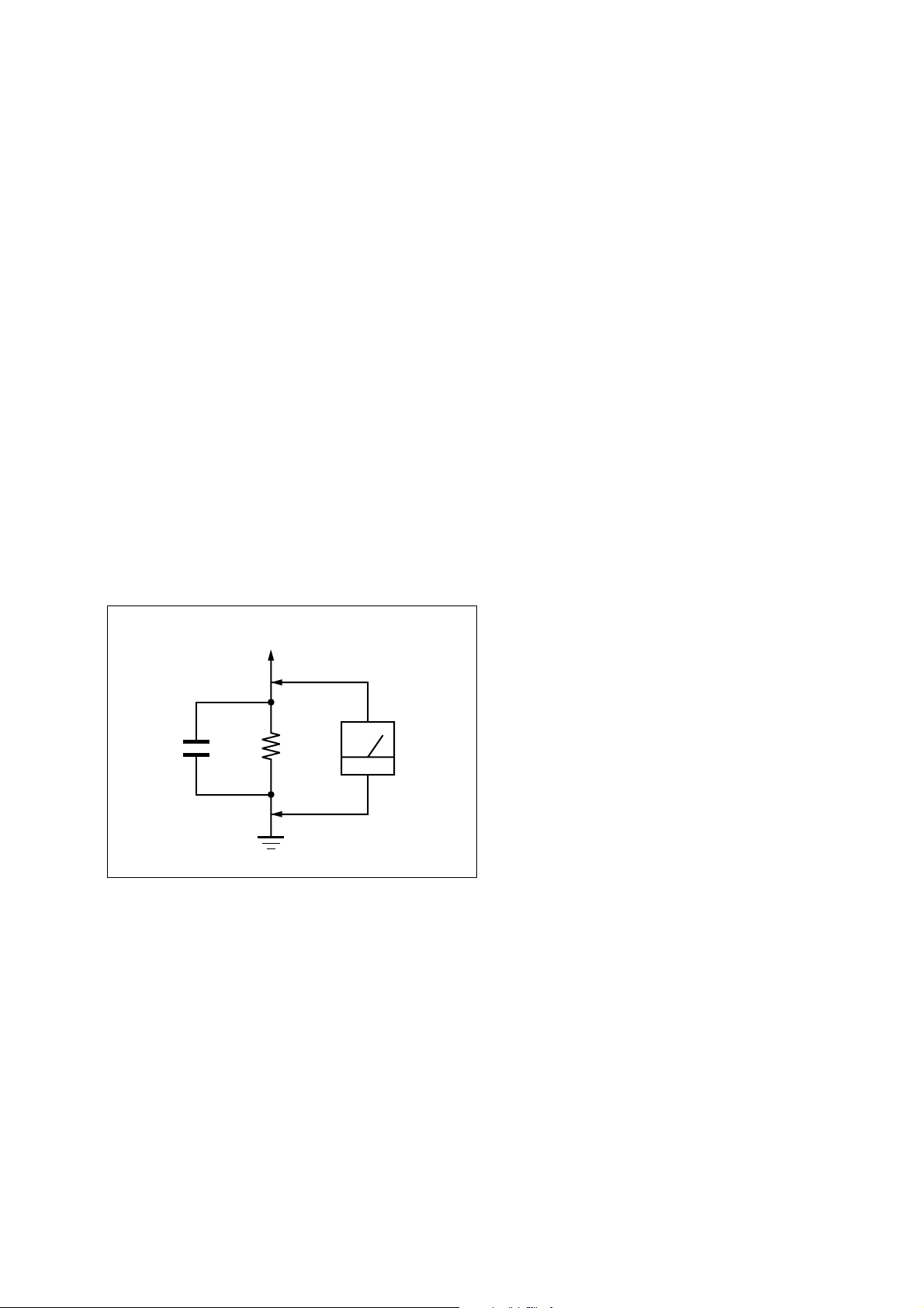
3. Measuring the voltage drop across a resistor by means of a
VOM or battery-operated A C voltmeter . The “limit” indication
is 0.75 V, so analog meters must have an accurate low-voltage
scale. The Simpson 250 and Sanwa SH-63Trd are examples
of a passive VOM that is suitable. Nearly all battery operated
digital multimeters that have a 2 V AC range are suitable. (See
Fig. A)
To Exposed Metal
Parts on Set
AC
0.15 µF
1.5 k
Ω
Earth Ground
voltmete
(0.75 V)
Fig. A. Using an AC voltmeter to check AC leakage.
SAFETY-RELATED COMPONENT WARNING!!
COMPONENTS IDENTIFIED BY MARK 0 OR DOTTED LINE
WITH MARK 0 ON THE SCHEMATIC DIAGRAMS AND IN
THE PARTS LIST ARE CRITICAL TO SAFE OPERATION.
REPLACE THESE COMPONENTS WITH SONY PARTS WHOSE
PART NUMBERS APPEAR AS SHOWN IN THIS MANUAL OR
IN SUPPLEMENTS PUBLISHED BY SONY.
ATTENTION AU COMPOSANT AYANT RAPPORT
LES COMPOSANTS IDENTIFIÉS P AR UNE MARQUE 0 SUR
LES DIAGRAMMES SCHÉMATIQUES ET LA LISTE DES
PIÈCES SONT CRITIQUES POUR LA SÉCURITÉ DE
FONCTIONNEMENT. NE REMPLACER CES COM- POSANTS
QUE PAR DES PIÈCES SONY DONT LES NUMÉROS SONT
DONNÉS DANS CE MANUEL OU D ANS LES SUPPLÉMENTS
PUBLIÉS PAR SONY.
À LA SÉCURITÉ!
TABLE OF CONTENTS
1. SERVICING NOTES .............................................. 5
2. GENERAL .................................................................. 8
3. DISASSEMBLY
3-1. Disassembly Flow .......................................................... 12
3-2. Case ................................................................................ 13
3-3. Front Panel Block........................................................... 13
3-4. CIS Board, Tuner (FM/AM)........................................... 14
3-5. D.AUDIO Board, DSP Board......................................... 14
3-6. TUNER Board, CONTROL Board ................................ 15
3-7. PREOUT Board, S_SPTM Board .................................. 15
3-8. D_VIDEO Board............................................................ 16
3-9. A_VIDEO Board............................................................ 16
3-10. MAIN Board, C_SPTM Board....................................... 17
3-11. AC Board, Power Transformer (T001)........................... 18
3-12. Power AMP Block .......................................................... 18
4. TEST MODE............................................................. 19
5. ELECTRICAL ADJUSTMENTS ........................ 23
6. DIAGRAMS
6-1. Block Diagram – CONTROL Section –......................... 25
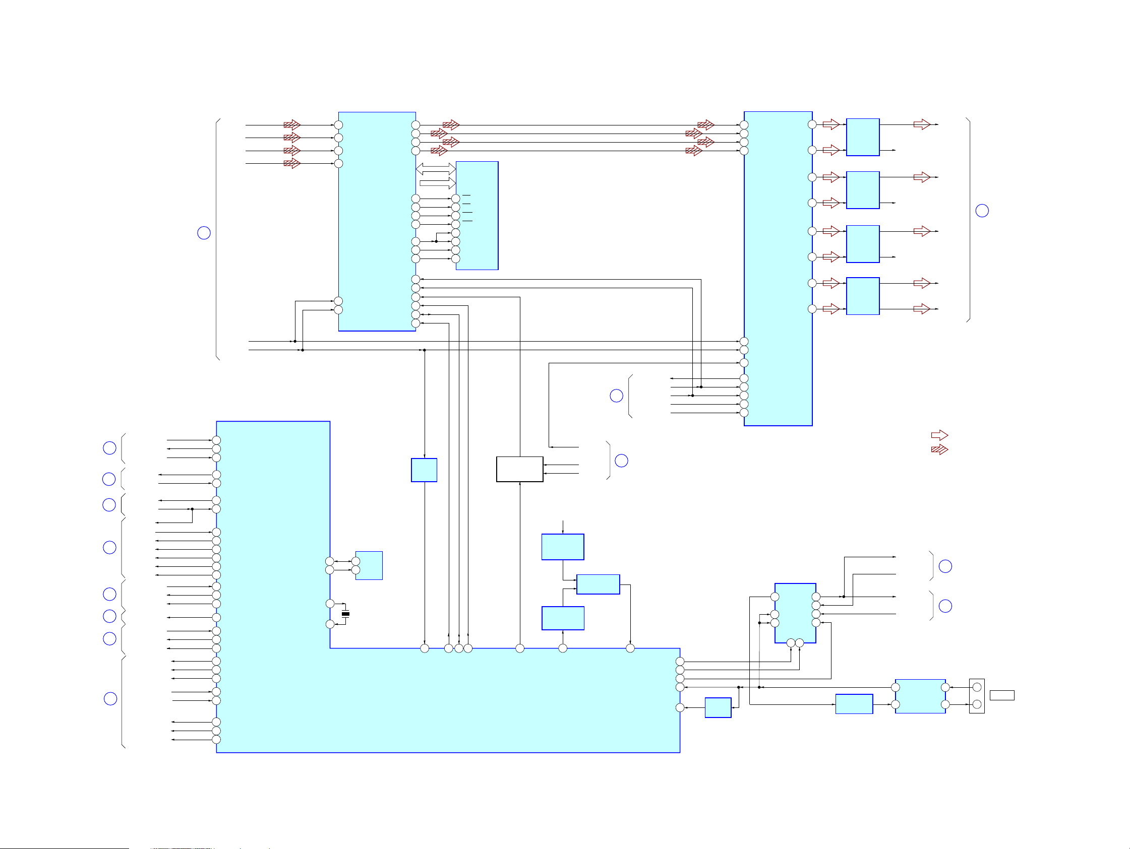
6-2. Block Diagram – DSP Section – .................................... 26
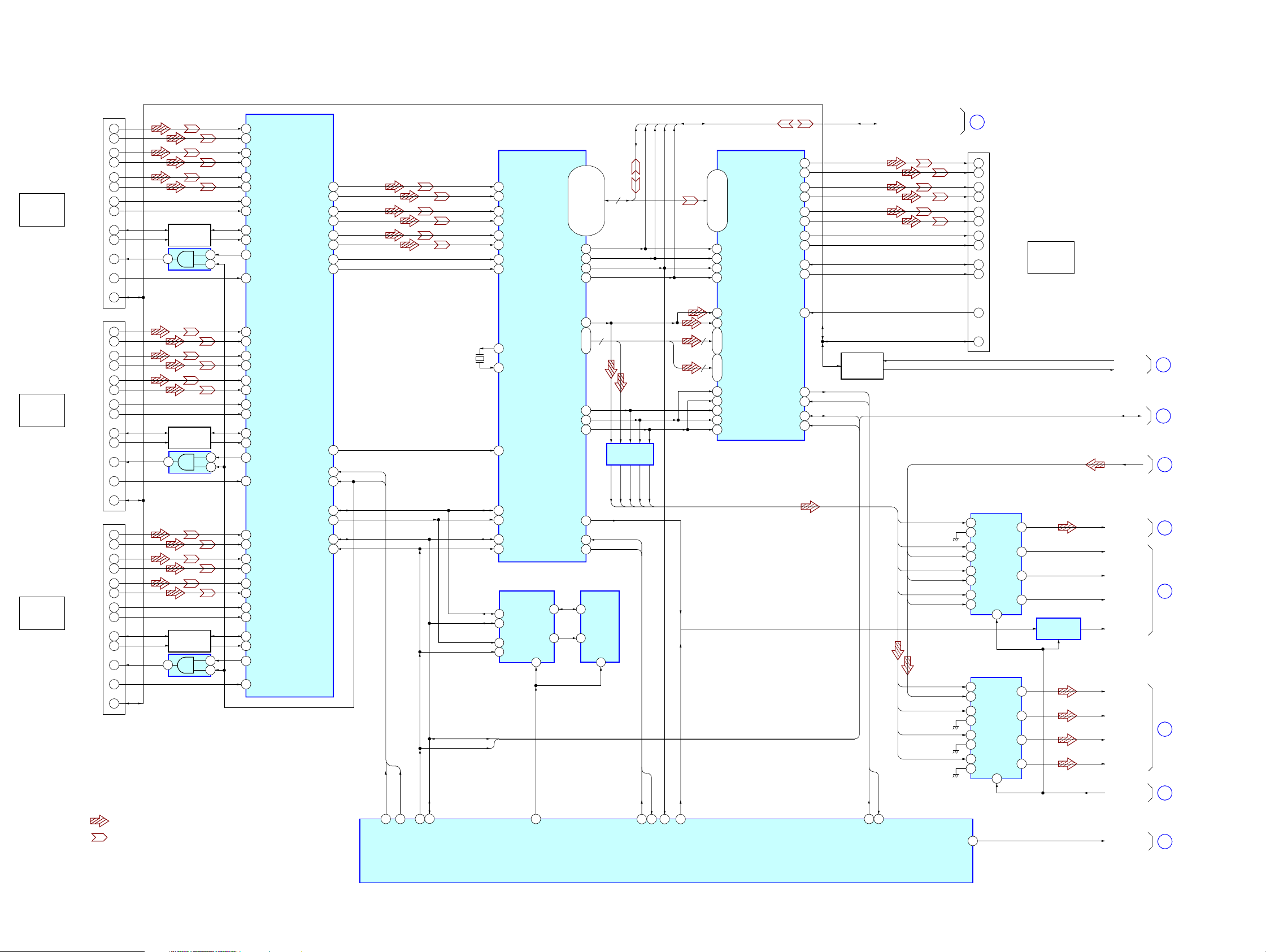
6-3. Block Diagram – DIGITAL AUDIO Section – .............. 27
6-4. Block Diagram – HDMI Section –................................. 28
6-5. Block Diagram – VIDEO PROCESS Section – ............. 29
6-6. Block Diagram – ANALOG AUDIO Section – ............. 30
6-7. Block Diagram – POWER AMP Section – .................... 31
6-8. Block Diagram – VIDEO Section – ............................... 32
6-9. Block Diagram – PANEL, CIS, XM/
SIRIUS RECEIVER, DMPORT Section – .................... 33
6-10. Block Diagram – POWER SUPPLY Section – .............. 34
6-11. Schematic Diagram – MAIN Board (1/4) – ................... 36
6-12. Schematic Diagram – MAIN Board (2/4) – ................... 37
6-13. Schematic Diagram – MAIN Board (3/4) – ................... 38
6-14. Schematic Diagram – MAIN Board (4/4) – ................... 39
6-15. Printed Wiring Board – MAIN Board – ......................... 40
6-16. Schematic Diagram – D.AUDIO Board (1/5) – ............. 41
6-17. Schematic Diagram – D.AUDIO Board (2/5) – ............. 42
6-18. Schematic Diagram – D.AUDIO Board (3/5) – ............. 43
6-19. Schematic Diagram – D.AUDIO Board (4/5) – ............. 44
6-20. Schematic Diagram – D.AUDIO Board (5/5) – ............. 45
6-21. Printed Wiring Board
– D.AUDIO Board (Component Side) – ........................ 46
6-22. Printed Wiring Board
– D.AUDIO Board (Conductor Side) –.......................... 47
6-23. Printed Wiring Board
– TUNER Board (Component Side) – ........................... 48
6-24. Printed Wiring Board
– TUNER Board (Conductor Side) – ............................. 49
6-25. Schematic Diagram – TUNER Board (1/2) – ................ 50
6-26. Schematic Diagram – TUNER Board (2/2) – ................ 51
6-27. Printed Wiring Board – DSP Board (Side A) – .............. 52
6-28. Printed Wiring Board – DSP Board (Side B) – .............. 53
6-29. Schematic Diagram – DSP Board (1/4) – ...................... 54
6-30. Schematic Diagram – DSP Board (2/4) – ...................... 55
6-31. Schematic Diagram – DSP Board (3/4) – ...................... 56
6-32. Schematic Diagram – DSP Board (4/4) – ...................... 57
6-33. Printed Wiring Boards – CONNECTOR Section –........ 58
6-34. Schematic Diagram – CONNECTOR Section – ............ 59
6-35. Printed Wiring Board
– TEMPERATURE DETECTION Board – ................... 60
3

STR-DA4300ES
6-36. Schematic Diagram
– TEMPERATURE DETECTION Board – ................... 60
6-37. Printed Wiring Board – A CLASS AMP Board – .......... 61
6-38. Schematic Diagram – A CLASS AMP Board (1/2) – .... 62
6-39. Schematic Diagram – A CLASS AMP Board (2/2) – .... 63
6-40. Printed Wiring Board – POWER AMP Board – ............ 64
6-41. Schematic Diagram – POWER AMP Board – ............... 65
6-42. Printed Wiring Board – PROTECTOR (F-C) Board – ... 66
6-43. Schematic Diagram – PROTECTOR (F-C) Board –...... 67
6-44. Printed Wiring Boards
– PROTECTOR (SB/SURR) Section – ........................... 68
6-45. Schematic Diagram
– PROTECTOR (SB/SURR) Section – .......................... 69
6-46. Printed Wiring Board – BIAS Board –........................... 70
6-47. Schematic Diagram – BIAS Board – ............................. 71
6-48. Printed Wiring Board – PREOUT Board – .................... 72
6-49. Schematic Diagram – PREOUT Board – ....................... 73
6-50. Printed Wiring Boards – SPEAKER Section – .............. 74
6-51. Schematic Diagram – SPEAKER Section –................... 75
6-52. Printed Wiring Board
– D_VIDEO Board (Component Side) – ....................... 76
6-53. Printed Wiring Board
– D_VIDEO Board (Conductor Side) – ......................... 77
6-54. Schematic Diagram – D_VIDEO Board (1/10) – .......... 78
6-55. Schematic Diagram – D_VIDEO Board (2/10) – .......... 79
6-56. Schematic Diagram – D_VIDEO Board (3/10) – .......... 80
6-57. Schematic Diagram – D_VIDEO Board (4/10) – .......... 81
6-58. Schematic Diagram – D_VIDEO Board (5/10) – .......... 82
6-59. Schematic Diagram – D_VIDEO Board (6/10) – .......... 83
6-60. Schematic Diagram – D_VIDEO Board (7/10) – .......... 84
6-61. Schematic Diagram – D_VIDEO Board (8/10) – .......... 85
6-62. Schematic Diagram – D_VIDEO Board (9/10) – .......... 86
6-63. Schematic Diagram – D_VIDEO Board (10/10) – ........ 87
6-64. Printed Wiring Board
– A_VIDEO Board (Component Side) –........................ 88
6-65. Printed Wiring Board
– A_VIDEO Board (Conductor Side) – ......................... 89
6-66. Schematic Diagram – A_VIDEO Board (1/4) –............. 90
6-67. Schematic Diagram – A_VIDEO Board (2/4) –............. 91
6-68. Schematic Diagram – A_VIDEO Board (3/4) –............. 92
6-69. Schematic Diagram – A_VIDEO Board (4/4) –............. 93
6-70. Printed Wiring Board – VIDEO3 Board –...................... 94
6-71. Schematic Diagram – VIDEO3 Board – ........................ 95
6-72. Printed Wiring Board
– CONTROL Board (Component Side) – ...................... 96
6-73. Printed Wiring Board
– CONTROL Board (Conductor Side) –........................ 97
6-74. Schematic Diagram – CONTROL Board (1/2) –........... 98
6-75. Schematic Diagram – CONTROL Board (2/2) –........... 99
6-76. Printed Wiring Board – CIS Board –.............................. 100
6-77. Schematic Diagram – CIS Board – ................................101
6-78. Printed Wiring Board – DISPLAY Board – ...................102
6-79. Schematic Diagram – DISPLAY Board – ...................... 103
6-80. Printed Wiring Boards – PANEL Section –.................... 104
6-81. Schematic Diagram – PANEL Section –........................105
6-82. Printed Wiring Board – DC-DC Board – ....................... 106
6-83. Schematic Diagram – DC-DC Board – .......................... 107
6-84. Printed Wiring Board – AC Board –............................... 108
6-85. Schematic Diagram – AC Board – .................................109
7. EXPLODED VIEWS
7-1. Case Section ................................................................... 156
7-2. DISPLAY Board Section................................................ 157
7-3. Front Panel Section ........................................................158
7-4. AC/DC-DC Boards Section............................................159
7-5. D.AUDIO/D_VIDEO Boards Section............................ 160
7-6. A_VIDEO Board Section...............................................161
7-7. Heat Sink Section ........................................................... 162
7-8. MAIN Board Section...................................................... 163
8. ELECTRICAL PARTS LIST............................... 164
4
SECTION 1
SERVICING NOTES
STR-DA4300ES
UNLEADED SOLDER
Boards requiring use of unleaded solder are printed with the leadfree mark (LF) indicating the solder contains no lead.
(Caution: Some printed circuit boards may not come printed with
the lead free mark due to their particular size)
: LEAD FREE MARK
Unleaded solder has the following characteristics.
• Unleaded solder melts at a temperature about 40 °C higher
than ordinary solder.
Ordinary soldering irons can be used but the iron tip has to be
applied to the solder joint for a slightly longer time.
Soldering irons using a temperature regulator should be set to
about 350 °C.
Caution: The printed pattern (copper foil) may peel away if
the heated tip is applied for too long, so be careful!
• Strong viscosity
Unleaded solder is more viscou-s (sticky, less prone to flow)
than ordinary solder so use caution not to let solder bridges
occur such as on IC pins, etc.
• Usable with ordinary solder
It is best to use only unleaded solder but unleaded solder may
also be added to ordinary solder.
NOTE OF REPLACING THE IC3601 ON THE
D_VIDEO BOARD
Replacement of IC3601 on the D_VIDEO board used in this set
requires a special tool.
NOTE OF REPLACING THE IC3511 AND IC3513 ON
THE D_VIDEO BOARD
IC3511 and IC3513 on the D_VIDEO board cannot exchange with
single. When IC3511 and IC3513 on the D_VIDEO board are
damaged, exchange the entire mounted board.
NOTE OF REPLACING THE IC5002 AND IC5202 ON
THE DSP BOARD
IC5002 and IC5202 on the DSP board cannot exchange with single.
When IC5002 and IC5202 on the DSP board are damaged, exchange
the entire mounted board.
UPDATE OF SOFTWARE OF IC2003 ON THE CONTROL BOARD, IC3610 ON THE D_VIDEO BOARD AND
IC5208 ON THE DSP BOARD
Perform operation of the following when the update of software of the IC2003 on the CONTR OL board, IC3610 on the D_VIDEO board and
IC5208 on the DSP board is necessary.
Connect:
for PC
Procedure:
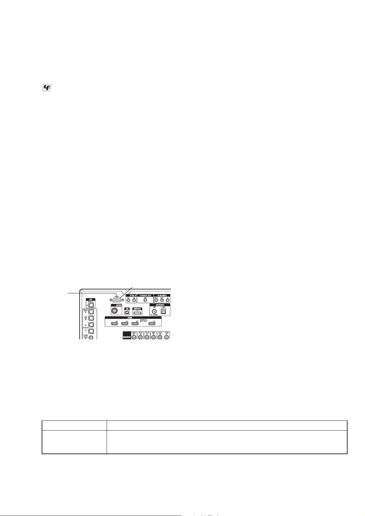
1. Connect J881 on the CIS board and PC by using the RS-232C cable.
2. Turn on the main power.
3. The update is executed by using PC.
4. When the update ends, turn off the main power.
5. Remove the RS-232C cable from the J881 on the CIS board and PC.
ERROR MESSAGES
If there is a malfunction, the display shows a code of two numbers and a message. You can check the condition of the system by the
message. Refer to the following table to solve the problem.
J881
messages cause and response
PROTECTOR Irregular current is output to the speakers, or the upper panel of the receiver is covered with something.
The receiver will automatically turn off after a few seconds. Cheack the speakers connection and turn
on the power again.
5
STR-DA4300ES
POWER AMP BLOCK SERVICE POSITION
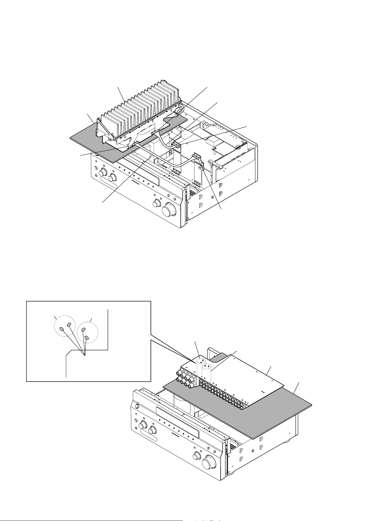
In checking the Power AMP block, prepare jig (extension cab le J-2501-291-A: 2 mm Pitch, 12 cores, Length 300 mm/J-2501-311-A: 2 mm
Pitch, 15 cores, Length 300 mm).
power AMP Block
insulating sheet
A CLASS AMP board
(CN1504)
Connect the extension jig (J-2501-291-A) to the
A CLASS AMP board (CN1504) and
CONNECTOR 3 board (CN1202).
A CLASS AMP board
(CN1505)
Connect the extension jig (J-2501-311-A) to the
A CLASS AMP board (CN1505) and
CONNECTOR 4 board (CN1207).
CONNECTOR 4 board
(CN1207)
CONNECTOR 3 board
(CN1202)
MAIN BOARD SERVICE POSITION
CAUTION
C1237
C1137
In checking the board, make two
capacitors discharge for electric
shock prevention. (R: 800
Ω
C1137
C1237
MAIN board
/2W)
insulating sheet
6
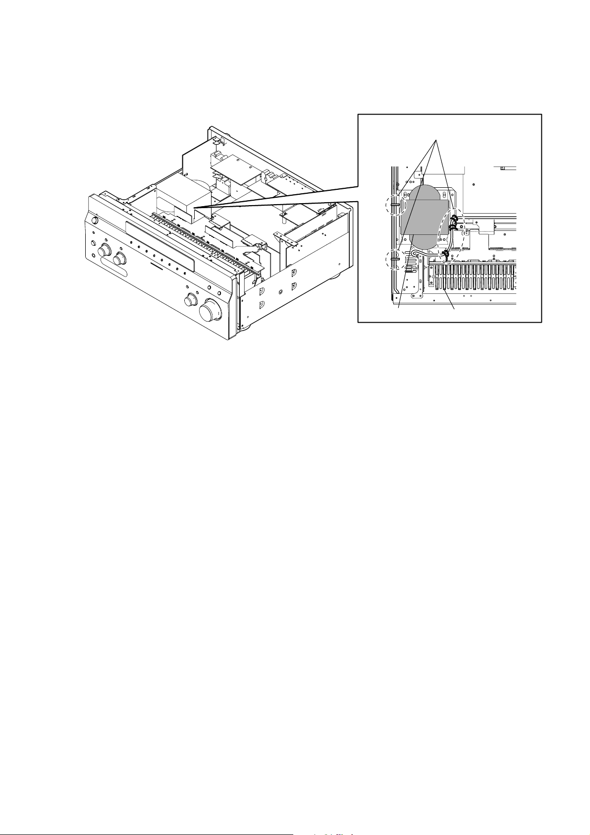
LEAD WIRE SETTING
STR-DA4300ES
The lead wire must not come in contact with the transformer and the heat sink.
Please band together so that a primary side cable
cannot touch a power transformer and heat sink.
transformer
heat sink
7
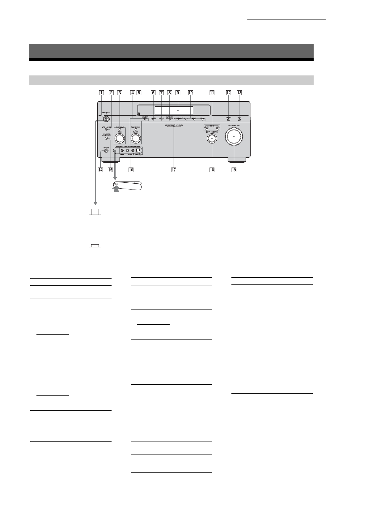
STR-DA4300ES
Getting Started
Description and location of parts
Front panel
SECTION 2
GENERAL
To remove the cover
Press PUSH.
When you remove the cover, keep it out
of reach from children.
Status of the POWER button
Off
The receiver is turned off (initial
setting).
Press POWER to turn the receiver on.
You cannot turn the receiver on using
the remote.
On/Standby
?/1 on the remote to turn the
Press
receiver on or set it to the standby mode.
When you press POWER on the
receiver, the receiver will be turned off.
This section is extracted from
instruction manual.
Name Function
A POWER Press to turn the
B AUTO CAL MIC
jack
C TONE MODE Adjusts FRONT/
TONE
D MEMORY/
ENTER
TUNING MODE
TUNING
E Remote sensor Receives signals from
F DIMMER Press repeatedly to
G DISPLAY Press repeatedly to
H SUR BACK
DECODING
receiver on or off.
Connects to the
supplied optimizer
microphone for the
Digital Cinema Auto
Calibration function.
CENTER/
SURROUND/
SURROUND BACK
BASS and TREBLE.
Press TONE MODE
repeatedly to select
BASS or TREBLE,
then turn TONE to
adjust the level.
Press to operate a tuner
(FM/AM) and satellite
radio (XM/SIRIUS).
remote commander.
adjust brightness of the
display.
select information
displayed on the
display.
Press to activate SB
DECODING.
Name Function
I Display
window
J 2CH/A.DIRECT Press to select sound
A.F.D.
MOVIE
MUSIC
K ZONE/
POWER,
SELECT
L DMPORT Press to select the
M HDMI Press to select input
N PHONES jack Connects to
O SPEAKERS
(OFF/A/B/A+B)
The current status of
the selected component
or a list of selectable
items appears here.
field.
Press SELECT
repeatedly to select
zone 2 or main zone.
Each time you press
POWER, the output
signals for the selected
zone will be turned on
or off.
audio/video input
signal from the
component connected
to the DIGITAL
MEDIA PORT adapter.
source from the
component connected
to the HDMI IN jack.
headphones.
Switch to OFF, A, B,
A+B of the front
speakers.
Name Function
P VIDEO 3 IN/
PORT ABLE AV
IN jacks
Q MULTI
CHANNEL
DECODING
lamp
R INPUT
SELECTOR
S MASTER
VOLUME
Connect to a portable
audio/video component
such as a camcorder or
video game.
Lights up when multichannel audio signals
are decoded.
Turn to select the input
source to play back.
To select the input
source for zone 2, press
ZONE/SELECT (
to select zone 2 first
(“ZONE 2 INPUT”
appears on the display),
then turn INPUT
SELECTOR to select
the input source.
Turn to adjust the
volume level of all
speakers at the same
time.
qa)
8
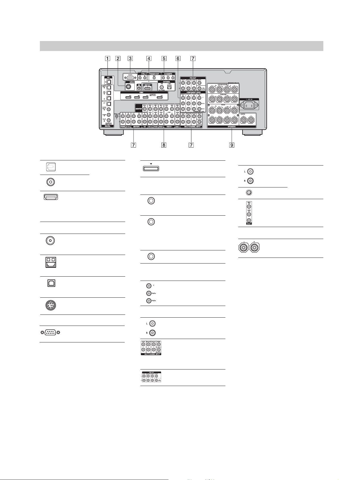
Rear panel
STR-DA4300ES
A DIGITAL INPUT/OUTPUT section
OPTICAL IN/
OUT jacks
COAXIAL IN
jacks
HDMI IN/
OUT* jacks
Connect to a DVD
player, Super Audio
CD player, etc. The
COAXIAL jack
provides a better
quality sound.
Connect to a DVD
player, Blu-ray Disc
Player, or a satellite
tuner. An image and
the sound are output
to TV or a projector.
B ANTENNA section
FM ANTENNA
jack
AM
ANTENNA
jack
XM jack Connects to the XM
SIRIUS jack Connects to a
Connects to the FM
wire antenna (aerial)
supplied with this
receiver.
Connects to the AM
loop antenna (aerial)
supplied with this
receiver.
Mini Tuner and
Home Dock (not
supplied).
SiriusConnect Home
tuner (not supplied).
C RS-232C port
Used for
maintenance and
service.
D DMPORT
Connects to a Sony
DIGITAL MEDIA
PORT adapter.
E Control jack for Sony equipment
and other external components
CTRL S IN/
OUT jacks
TRIGGER
OUT jack
IR REMOTE
IN/OUT jacks
Connect to Sony TV ,
DVD player or VCR
with CONTROL S
jack.
Connect to interlock
on/off of the power
supply of other 12V
TRIGGER compliant
components, or the
amplifier/receiver of
zone 2.
Connect an IR
repeater.
F COMPONENT VIDEO INPUT/
OUTPUT section
Y, PB/CB, PR/
C
IN/OUT*
R
jacks
Connect to a DVD
player, TV, or a
satellite tuner.
G AUDIO INPUT/OUTPUT section
AUDIO IN/
OUT jacks
MULTI
CHANNEL
INPUT jacks
PRE OUT jacks Connect to an
Connect to a tape
deck or MD deck, etc.
Connect to a Super
Audio CD player or
DVD player with an
analog audio jack for
7.1 channel or 5.1
channel sound.
external power
amplifier.
H VIDEO/AUDIO INPUT/OUTPUT
section
AUDIO IN/
OUT jacks
VIDEO IN/
OUT* jacks
AUDIO OUT
jacks
VIDEO OUT
jack
Connect to a VCR or
a DVD player etc.
Connect to the
component in zone 2.
I SPEAKERS section
Connects to speakers.
*You can watch the select ed inpu t image when you
connect the MONITOR VIDEO OUT jack to a TV.
You can operate this receiver using a GUI
(Graphical User Interface).
9
STR-DA4300ES
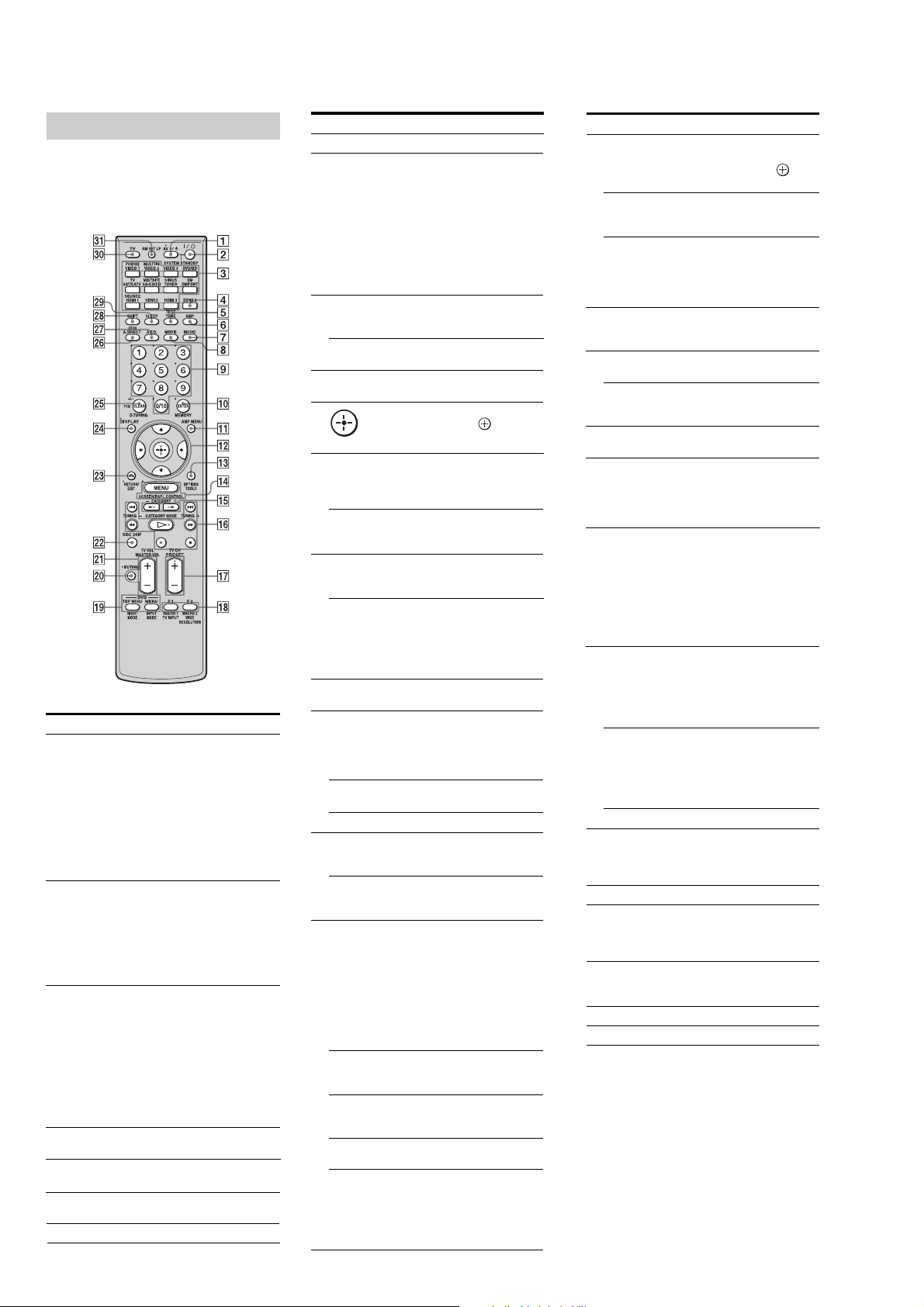
Remote commander
You can use the supplied remote RM-AAL011 to
operate the receiver and to control the Sony
audio/video components that the remote is
assigned to operate.
RM-AAL011
Name Function
A AV ?/1 (on/
standby)
B ?/1 (on/
standby)
C Input
buttons
D ZONE 2 Press to enable the zone 2
E TEST TONE Press to output the test tone from
F AMP Press to enable the receiver
G MUSIC Press to select sound field.
Press to turn on or off the audio/
video components that the remote
is assigned to operate. If you press
the ?/1 (B) at the same time, it
will turn off the receiver and
other Sony components
(SYSTEM STANDBY).
Note
The function of the AV ?/1 switch
changes automatically each time
you press the input button (C).
Press to turn the receiver on or off.
If ZONE 2 is selected, only the
main receiver is turned on or off
with this button. To turn off all
components including an amplifier
in zone 2, press ?/1 and AV?/1
(A) at the same time
(SYSTEM STANDBY).
Press one of the buttons to select
the component you want to use.
Press a pink-labeled button after
pressing SHIFT (wk). When you
press any of the input buttons, the
receiver turns on. The buttons are
factory assigned to control Sony
components. You can program the
remote to control non-Sony
components following the steps in
“Programming the remote”.
operation.
each speaker.
operation.
Name Function
H MOVIE Press to select sound field.
I Numeric
buttons
J ENTER Press to enter the value after
MEMORY Press to store a station during
K AMP MENU Press to display the menu to
L
V/v/B/b
M OPTIONS Press to display and select items
TOOLS Press to display and select items
N MENU Press to display the menu to
SCREEN/
DSPL
CONTROL
O CATEGORY
+/–
P m/M
a)
x
a)
X
a) b)
H
./>
CATEGORY
MODE
TUNING +/– Press to select station.
Q PRESET
b)
/–
+
TV CH +/– Press TV (e;), then press TV CH
R F1/F2 Press TV (e;), then press F1 or F2
MACRO1,
MACRO2
TV/INPUT Press TV/INPUT and TV (e;) at
WIDE Press repeatedly to select the
RESOLUTION
Press to
− preset/tune to preset stations.
− select track numbers of the CD
player, DVD player, Blu-ray
Disc Player or MD deck. Press
0/10 to select track number 10.
− select channel numbers of the
VCR or satellite tuner.
− After pressing TV (e;), press
the numeric buttons to select
the TV channels.
selecting a channel, disc or track
using the numeric buttons.
tuner operation.
operate the receiver.
Press V/v/B/b to select the menu
items. Then press to enter the
selection.
from option menus for receiver
and DVD player, Blu-ray Disc
Player.
from the option menus for DVD
player or Blu-ray Disc Player, etc.
operate the audio/video
components.
Press SHIFT (wk), then press
MENU to switch the display mode
of the menu between SCREEN (to
display the menu on the TV screen)
and DSPL (to display the menu
in the display window).
Press to select the category for
satellite tuner.
a)
Press to operate the DVD player,
Blu-ray Disc Player, CD player,
MD deck, tape deck, or component
connected to the DIGITAL
a)
MEDIA PORT adapter etc.
Press to select the category mode
for satellite tuner.
Press to register FM/AM/satellite
tuner stations or to select preset
stations.
+/− to operate the TV, satellite
tuner, VCR, etc.
to select a component to operate.
• HDD recorder
F1: HDD
F2: DVD player, Blu-ray Disc
Player
• DVD/VHS combo player
F1: DVD player, Blu-ray Disc
Player
F2: VHS
Press AMP (6), then press
MACRO 1 or MACRO 2 to set
up the macro function.
the same time to select the input
signal (TV input or video input).
wide picture mode.
Press SHIFT (wk), then press
RESOLUTION repeatedly to
change the resolution of signals
output from the HDMI OUT or
COMPONENT VIDEO
MONITOR OUT jack.
Name Function
S DVD/
TOP MENU,
MENU
NIGHT
MODE
INPUT
MODE
T MUTING Press to turn off the sound
U MASTER
VOL +/–
TV VOL +/– Press TV (e;), then press TV
V DISC SKIP Press to skip a disc when using a
W RETURN/
EXIT O
X DISPLAY Press to select information
Y CLEAR Press to
>10 Press to select
D.TUNING Press to enter direct tuning mode.
Z 2CH/
A.DIRECT
wj A.F.D. Press to select sound field.
wk SHIFT Press to light up the button. It
wl SLEEP Press to activate the sleep timer
e; TV Press to enable the TV operation.
ea RM SET UP Press to set up the remote.
a)
See the table on page123 for information on the
buttons that you can use to control each component.
b)
The tactile dot is attached to these buttons (H,
PRESET+). Use as a mark of opera t ion.
Press to display the menus of the
DVD player on the TV screen.
Then use V/v/B/b and
perform a menu operations.
Press AMP (6), then press
NIGHT MODE to activate the
NIGHT MODE function.
Press AMP (6), then press
INPUT MODE to select the input
mode when the same components
are connected to both digital and
analog jacks.
temporarily. Press the button again
to restore the sound.
Press to adjust the volume level of
all speakers at the same time.
VOL +/− to adjust the volume level
of the TV.
multi-disc changer.
Press to return to the previous menu
or exit the menu while the menu or
on-screen guide of the VCR, DVD
player, or satellite tuner is
displayed on the TV screen.
displayed in the display window,
TV screen of the VCR, satellite
tuner, CD player, DVD player,
Blu-ray Disc Player, or MD deck.
Note
In the SCREEN mode, press the
button to display the menu on
the TV screen.
− clear a mistake when you press
the incorrect numeric button.
− return to continuous playback,
etc. of the satellite tuner or
DVD player.
− track numbers over 10 of the
VCR, satellite tuner, CD player
or MD deck.
− channel numbers of the Digital
CATV terminal.
Press to select sound field or to
switch the audio of the selected
input to analog signal without any
adjustment.
changes the remote button function
to activate the buttons with pink
printing.
function and the duration which the
receiver turns off automatically.
to
Notes
•Some functions explained in this section may not
work depending on the model.
•The above explanation is intended to serve as an
example only. Therefore, depending on the component,
the above operation may not be possible or may
operate differently than described.
10
STR-DA4300ES
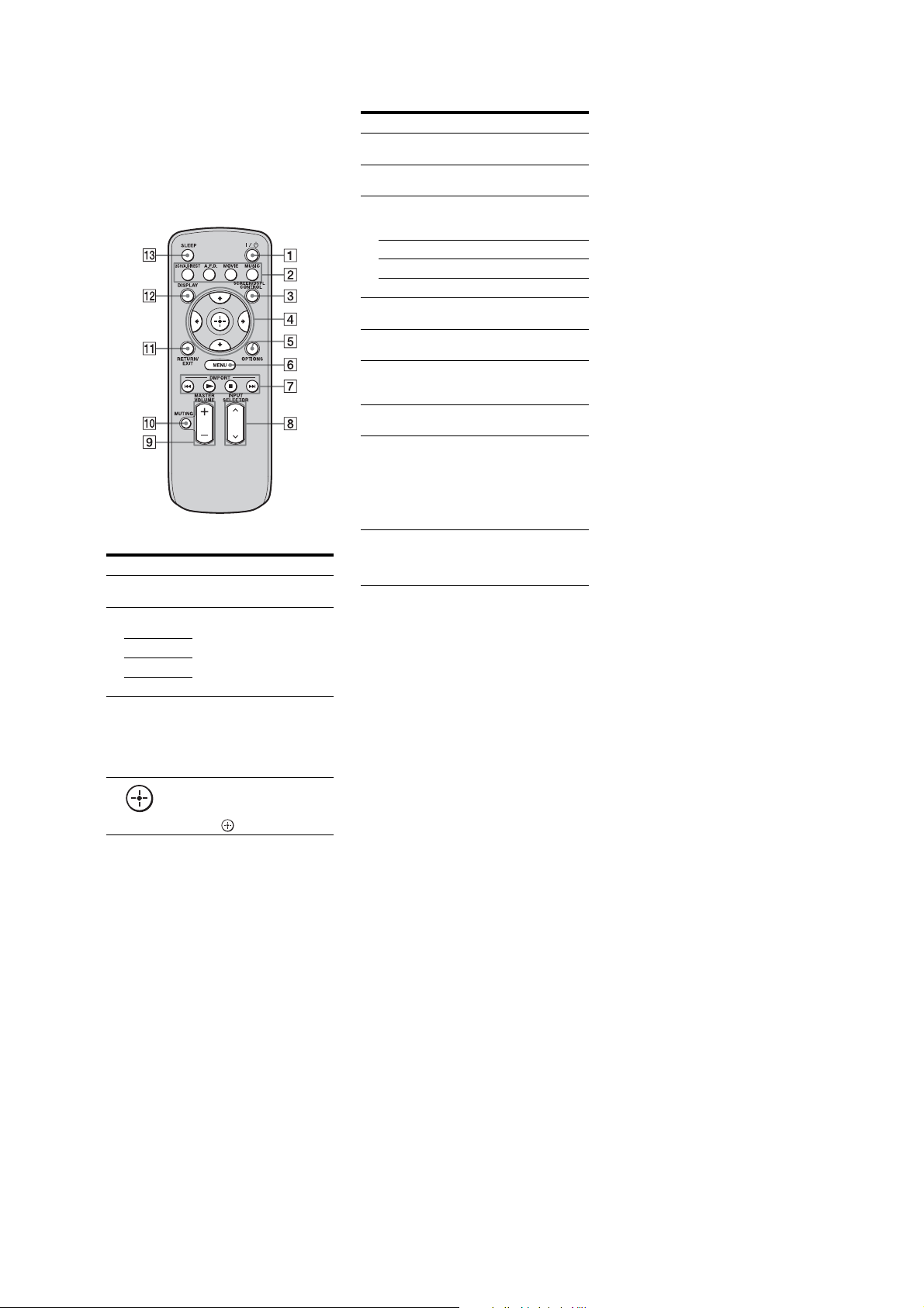
RM-AAU018
This remote can only be used to operate the
receiver. Y ou can control the main functions of
the receiver with simple operations using this
remote.
Name Function
A ?/1 (on/
standby)
B 2CH/
A.DIRECT
A.F.D.
MOVIE
MUSIC
C SCREEN/
DSPL
CONTROL
D
V/v/B/b
Press to turn a receiver on or off.
Press to select sound field.
Press to switch the display
mode of the menu between
SCREEN (to display the menu
on the TV screen) and DSPL (to
display the menu in the d isp la y
window).
After pressing SCREEN/DSPL
CONTROL (3), press V/v/B/
b to select the menu item. Then
press to enter the selection.
Name Function
E OPTIONS Press to display and select items
F MENU Press to displa y th e menu to
G DMPORT Press to operate the component
N Sta rts pl ay.
x Stops play.
./> Skips tracks.
H INPUT
SELECTOR
I MASTER
VOLU ME + /–
J MUTING Press to turn off the sound
K RETURN/
EXIT
L DISPLAY Press to select information
M SLEEP Press to acti v at e the sleep timer
from option menus.
operate the receiver.
connected to the DIGITAL
MEDIA PORT adapter.
Press to select the input source
to play back.
Press to adjust the vo lume le v el.
temporarily. Press the button
again to restore the sound.
Press to return to the previous
menu or exit the menu.
displayed in the display
window.
Note
In the SCREEN mode, press the
button to display the menu on
the TV screen.
function and the duration which
the receiver turns off
automatically.
11
STR-DA4300ES
SECTION 3
DISASSEMBLY
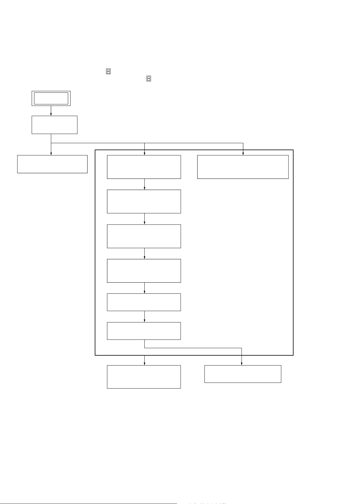
• This set can be disassembled in the order shown below.
3-1. DISASSEMBLY FLOW
Note 1: The process described in can be performed in any order.
Note 2: Without completing the process described in , the next process can not be performed.
SET
3-2. CASE
(Page 13)
3-3. FRONT PANEL BLOCK
(Page 13)
3-4. CIS BOARD,
TUNER (FM/AM)
(Page 14)
3-5. D.AUDIO BOARD,
DSP BOARD
(Page 14)
3-6. TUNER BOARD,
CONTROL BOARD
(Page 15)
3-7. PREOUT BOARD,
S_SPTM BOARD
(Page 15)
3-8. D_VIDEO BOARD
(Page 16)
3-9. A_VIDEO BOARD
(Page 16)
3-11. AC BOARD,
POWER TRANSFORMER (T001)
(Page 18)
12
3-10. MAIN BOARD,
C_SPTM BOARD
(Page 17)
3-12. POWER AMP BLOCK
(Page 18)
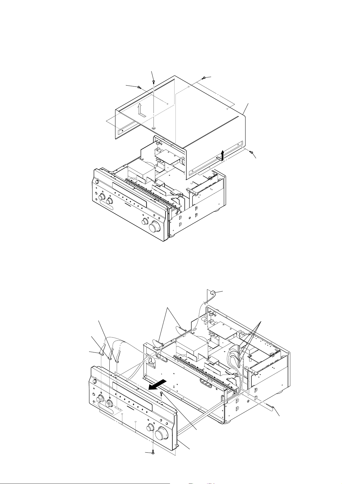
Note: Follow the disassembly procedure in the numerical order given.
3-2. CASE
3
flat head screw
(TP)
1
two screws
(BVST4
×
8)
4
2
two flat head screws
(TP)
4
5
STR-DA4300ES
case
1
two screws
(BVST4
×
8)
3-3. FRONT PANEL BLOCK
8
connector
(CN725)
9
connector
(CN728)
q;
connector
(CN721)
5
five screws
(BVTP3
×
3
connector
(CNP53)
1
two clamps
4
three connectors
(CN2015, CN2016, CN2017)
7
2
clamp
6
two screws
(BVTP3
qa
8)
front panel block
×
8)
13
STR-DA4300ES
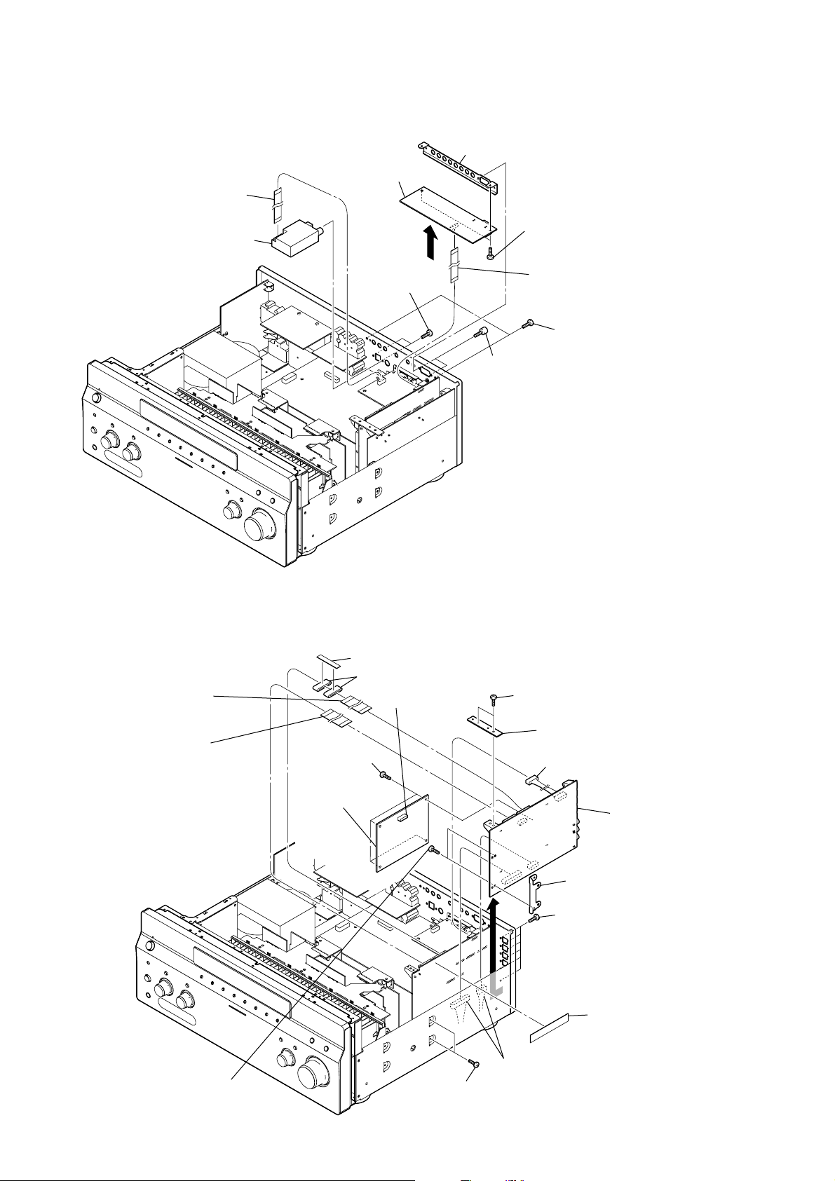
3-4. CIS BOARD, TUNER (FM/AM)
8
wire (flat type) (9 core)
(TUNER board (CN8004),
tuner (FM/AM))
q;
tuner (FM/AM)
7
9
two screws
(BVTT2.6
CIS board
3
×
6
bracket (CIS PC board)
5
two screws
(BVTP3
6)
1
4
two screws
(supplied with RS-232C connector)
×
8)
wire (flat type) (11 core)
(CONTROL board (CN2004),
CIS board (CN801))
2
two screws
(BVTP3
×
8)
3-5. D.AUDIO BOARD, DSP BOARD
4
wire (flat type) (25 core)
(D.AUDIO board (CN2201),
CONTROL board (CN2018))
7
wire (flat type) (23 core)
(D.AUDIO board (CN2202),
CONTROL board (CN2019))
qd
four screws
(BVTP3
qg
DSP board
5
saranet cushion
6
two ferrite cores
qf
×
8)
connector
(CN1)
qa
1
two screws
(BVTP3
2
8
×
8)
SUPPORT board
connector (CN2020)
qk
D.AUDIO board
qj
bracket (AC)
q;
six screws
(BVTP3
×
8)
3
saranet cushion
14
qh
two screws
(BVTP3
qs
two connectors
9
×
8)
two screws
(BVTP3
(CN2204, CN2207)
×
8)
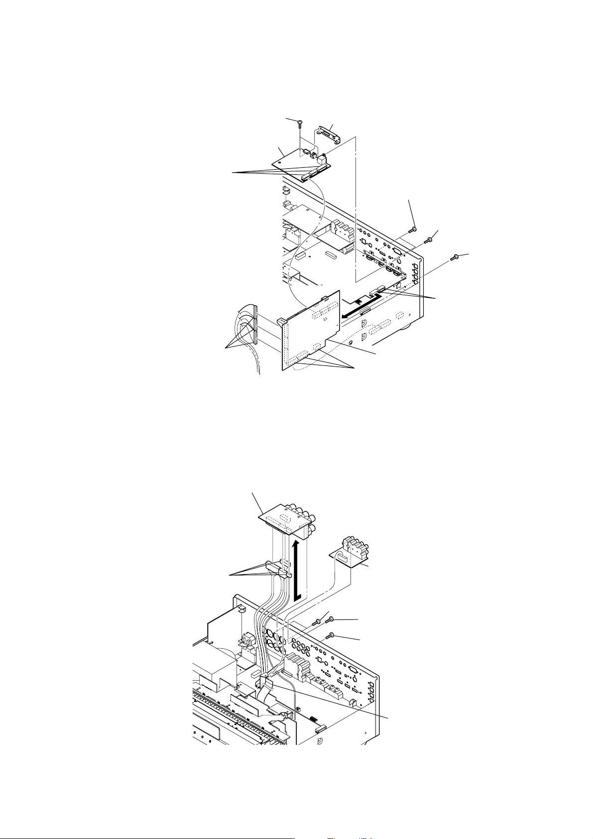
3-6. TUNER BOARD, CONTROL BOARD
4
two screws
(BVTP3
6
TUNER board
3
three connectors
(CN8006, CN8007, CN8008)
STR-DA4300ES
×
8)
5
bracket (digital-tuner)
2
two screws
(BVTP3
×
8)
1
screw
(B3
×
6)
8
screw
(BVTP3
9
two connectors
(CN3505, CN3801)
×
8)
7
three connectors
(CN2015, CN2016, CN2017)
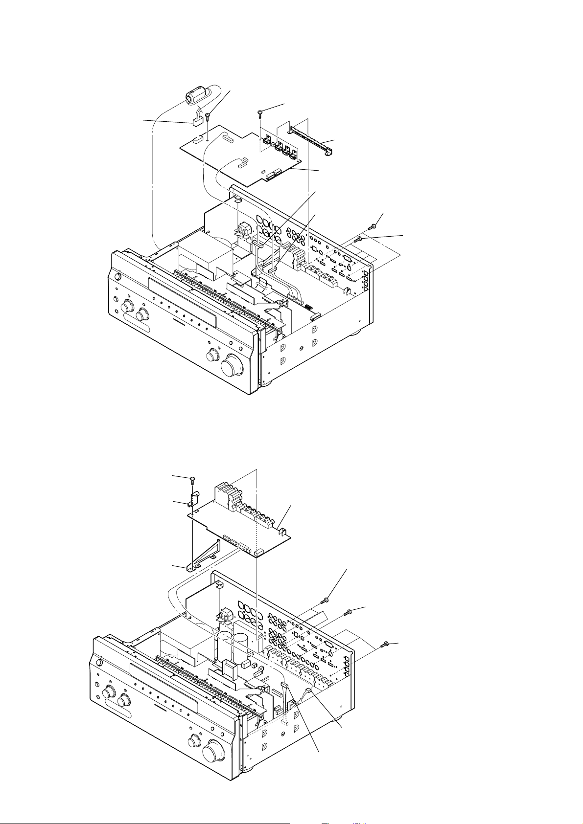
3-7. PREOUT BOARD, S_SPTM BOARD
7
S_SPTM board
6
four connectors
(CN4001, CN4002
CN4003, CN4004)
5
qa
q;
three connectors
(CN2008, CN2009, CN2010)
3
4
two screws (BV/ring)
2
screw
(BVTP3
2
screw
(BVTP3
CONTROL board
PREOUT board
×
8)
×
8)
1
wire (flat type) (19 core)
(CN4051)
15
STR-DA4300ES
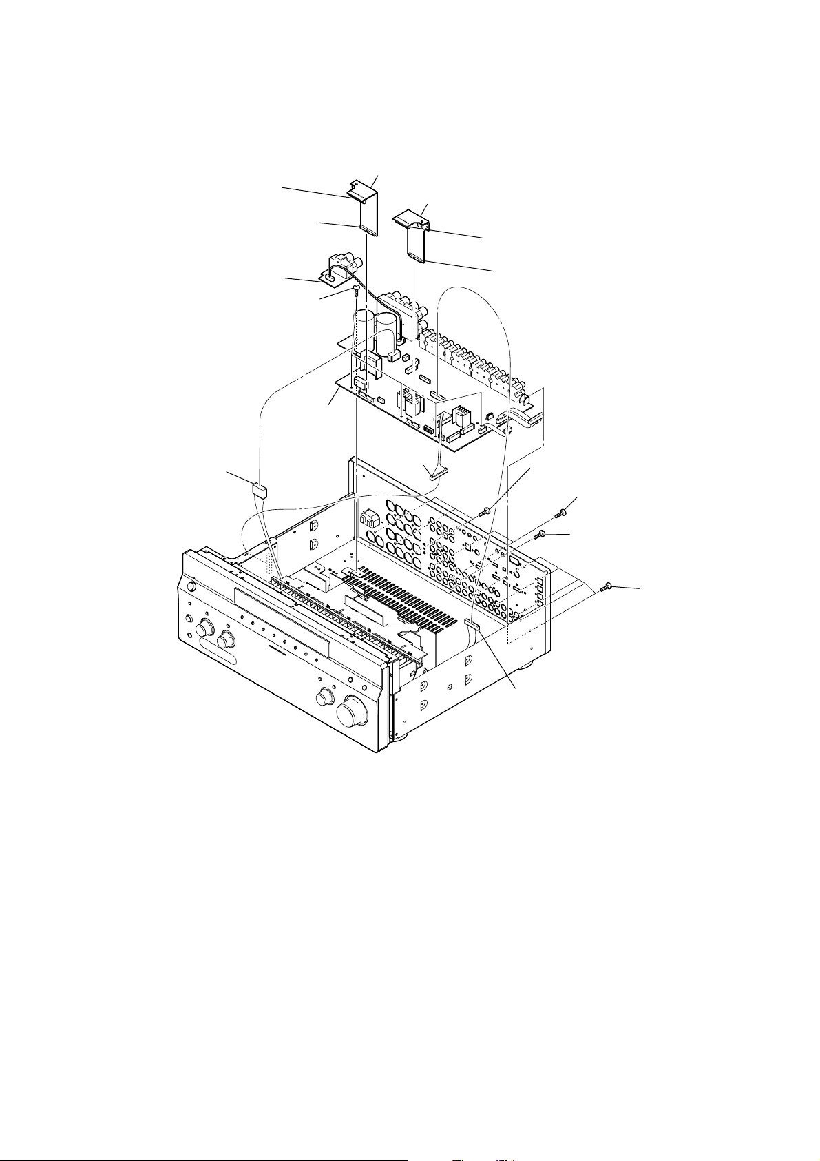
3-8. D_VIDEO BOARD
1
connector
(CN3508)
6
screw
(BVTP3
×
8)
7
two screws
(BVTP3
×
8)
8
9
D_VIDEO board
2
connector
(CN3506)
3
connector
(CN3602)
bracket (HDMI-A13)
5
two screws
(BVTP3
4
×
8)
four screws
(B3
×
6)
3-9. A_VIDEO BOARD
4
screw
(BVTP3
6
bracket (video PWB)
5
reinforcement (audio)
×
8)
7
A_VIDEO board
3
four screws
(BVTP3
3
×
8)
screw
(BVTP3
3
×
8)
three screws
(BVTP3
×
8)
16
2
connector
(CN6204)
1
connector
(CN6501)
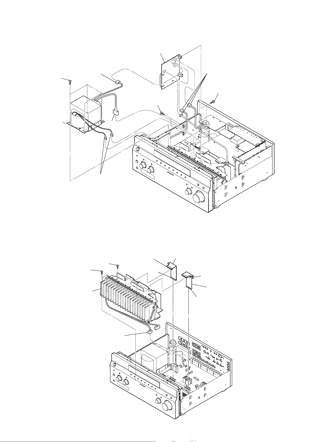
3-10. MAIN BOARD, C_SPTM BOARD
1
connector
(CN1207)
2
connector
(CN1204)
qd
C_SPTM board
qs
five screws
(BVTP3
qf
MAIN board
×
8)
3
CONNECTOR 4 board
6
CONNECTOR 3 board
4
connector
(CN1202)
5
STR-DA4300ES
connector
(CN1203)
8
connector
(CN1005)
7
connector
(CN1401)
q;
9
connector
(CN1020)
three screws
(BV/ring)
qa
two screws
(BVTP3
qa
screw
(BVTP3
×
8)
×
8)
qa
five screws
(BVTP3
×
8)
17
STR-DA4300ES
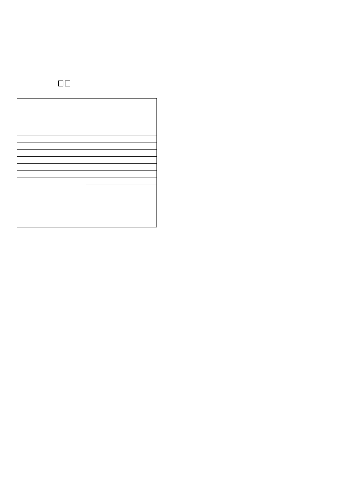
3-11. AC BOARD, POWER TRANSFORMER (T001)
2
connector
8
four screws
(BVTT4
9
power transformer
(T001)
×
8)
(CNP02)
6
connector
(CN1002)
4
5
two screws
(BVTP3
×
AC board
8)
1
three connectors
(CNP51, CNP53, CNP54)
3
two screws
(BVTP3
×
8)
3-12. POWER AMP BLOCK
8
8
four screws
(BVTP3
9
power AMP block
7
two connectors
(CN1001, CX1402)
three screws
(BVTP3
×
×
8)
1
connector
8)
(CN1207)
2
connector
(CN1204)
3
CONNECTOR 4 board
6
5
connector
(CN1203)
CONNECTOR 3 board
4
connector
(CN1202)
18
7
connector
(CN1005)

SECTION 4
TEST MODE
STR-DA4300ES
MEMORY CLEARING MODE
All preset contents are cleared when this mode is activated. Use
this mode before returning the product to clients upon completion
of repair.
Procedure:
1. While pressing the [TONE MODE] and [DMPORT] buttons, press
the [POWER] button to turn on the main power.
2. The message “MEMORY CLEARING***” appears and the
memories are reset to the default values.
3. When done, the message “MEMORY CLEARED*” appears.
FLUORESCENT INDICATOR TUBE PATTERN
CHECK MODE
All fluorescent segments are tested. When this test is activated, all
segments turn on at the same time, then each segment turns on one
after another.
Procedure:
1. While pressing the [MOVIE] and [DMPORT] buttons, press the
[POWER] button to turn on the main power.
2. All segments and all LEDs turn on.
SOUND FIELD CLEAR MODE
The preset sound field is cleared when this mode is activated. Use
this mode before returning the product to clients upon completion
of repair.
Procedure:
1. While pressing the [MUSIC] button, press the [POWER] button
to turn on the main power.
2. The message “S. F. Initialize” appears and initialization is
performed.
TUNER AM STEP CHANGE (9 kHz/10 kHz) MODE
Either the 9 kHz step or 10 kHz step can be selected for the AM
channel step.
Procedure:
1. Press the [POWER] button to turn on the main power.
2. Turn the [INPUT SELECTOR] dial to select the “AM”.
3. Press the [POWER] button to turn off the main power.
4. While pressing the [TUNING MODE] button, press the [POWER]
button to turn on the main power.
5. Either the message “AM 9kHz Step” or “AM 10kHz Step”
appears, select the desired step.
COMMAND MODE CHANGE MODE
The command mode of the remote-commander which this set
receives can be changed.
Procedure:
1. While pressing the [2CH/A. DIRECT] button, press the [POWER]
button to turn on the main power.
2. Either the message “COMMAND MODE [AV1]” or
“COMMAND MODE [AV2]” appears. Select the desired
mode.
SF LOCK ON/OFF CHANGE MODE
Procedure:
1. While pressing the [MUSIC] and [DMPORT] buttons, press the
[POWER] button to turn on the main power.
2. Either the message “SF LOCK [OFF]” or “SF LOCK [ON]”
appears.
XM FACTORY TEST MODE
Mode to confirm operation of XM. Doing display of ID of XM
antenna and output of audio signal that XM antenna generates, it is
confirmed that there are no probrems in the communication of the
XM antenna and the tranmission of the audio signal.
Procedure:
1. The XM antenna was connected, while pressing the [TUNING
MODE] and [MOVIE] buttons, press the [POWER] button to
turn on the main power.
2. Whenever the [DISPLAY] button is pressed, the output of the
audio signal of 1 kHz L/R, 20 Hz L/R, 5 kHz L/R, muting, 1
kHz L and 1kHz R are switched.
SIRIUS FACTORY TEST MODE
Mode to confirm operation of SIRIUS. Doing display of ID of
SIRIUS antenna and output of audio signal that SIRIUS antenna
generates, it is confirmed that there are no probrems in the
communication of the SIRIUS antenna and the tranmission of the
audio signal.
Procedure:
1. The SIRIUS antenna was connected, while pressing the
[TUNING MODE] and [A.F.D.] buttons, press the [POWER] button
to turn on the main power.
2. Whenever the [DISPLAY] button is pressed, the output of the
audio signal of 1 kHz L/R, 20 Hz L/R, 5 kHz L/R, muting, 1
kHz L and 1 kHz R are switched.
DIGITAL MEIDA PORT TEST
Procedure:
1. Connect the DMPORT check jig (P/N: J-2501-309-A) with
the DMPORT jack (CN8003) on the TUNER board.
2. While pressing the [A.F.D.] and [DMPORT] buttons, press the
[POWER] button to turn on the main power.
3. The message “DMPORT OK.” appears on the fluorescent
indicator tube and enter the digital media port test mode.
(Confirmation of communication line)
When “NO DETECT”, “UART NG” and “UART TO” are
displayed on the fluorescent indicator tube, confirm the
connection of the DMPORT check jig, and enter the mode
again.
Each time the
the connect check and adaptor version check are switched.
Press the . button on the remote commander, connected
confirmation of the DMPORT check jig is done again.
4. To a pinjack of the DMPORT check jig input information
relevant to audio signal (sine-wave 1.0V rms) and composite
video signal (white 100% 1.0Vp-p, color bar, etc.).
5. Confirm the output of speakers and monitor TV. (Confirmation
of analog signal)
6. To exit from this mode, press the x button on the remote
color
pattern
generator
AF
oscillator
> button on the remote commander is pressed,
J001
TUNER board
CN8003
DMPORT
check jig
(Part No.:
J-2501-309-A)
A_VIDEO board
set
J6004
TV
monitor
FL/FR
speaker
MAIN board
TB1001
19
STR-DA4300ES
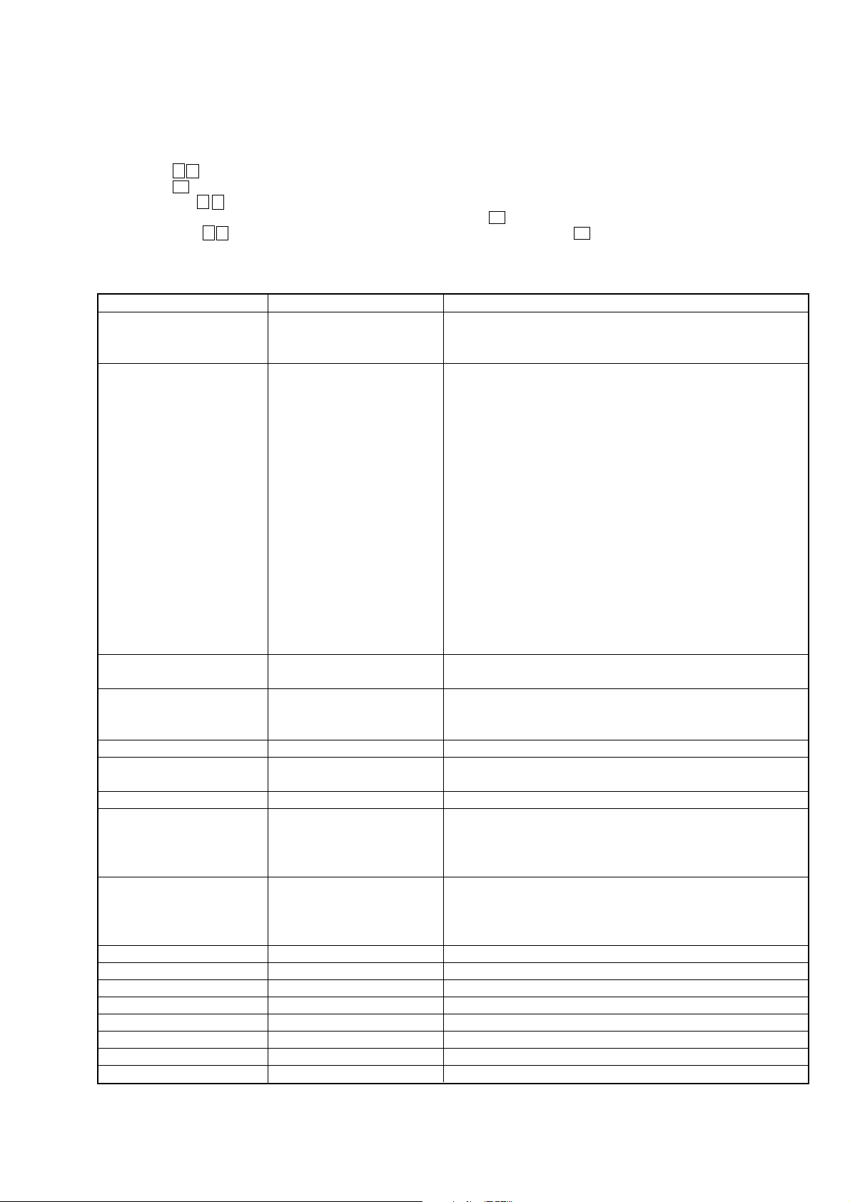
HISTORY MODE
The state that the set is used is memorized.
Procedure:
1. While pressing the [MUSIC] and [MEMORY/ENTER] buttons,
press the [POWER] button to turn on the power and
“HISTORY MODE” is displayed.
2. Each time the M m ke y of remote commander is pressed, the
item is switched in order as follows.
Items Display
Number of protector is generated PRCT COUNT: XXX
Total use time TTL_TIME: XXXXH XXM
Sound field setting XXXXXXXXXXXXXXXX
Input when protect is detected INPUT: XXXXXXXXXX
Input mode setting INMODE: XXXXXXXXXXXX
Input mode under lick state DSEL: XXXXXXXXXXXXXXX
Stream under input STREAM: XXXXXXX
Channel information CONFIG:XXXXXXX
State of headphone HEAD PHONES: XXX
Volume VOL: XXXdB
EQ setting value
Level collection value Lv SL/SR XXXX/XXXX
each channel Lv CT/SW XXXX/XXXX
Total time of power on TTL_P_ON: XXXXH XXM
BASS: XXXdB
TREB: XXXdB
Lv FL/FR XXXX/XXXX
Lv BL/BR XXXX/XXXX
20
STR-DA4300ES
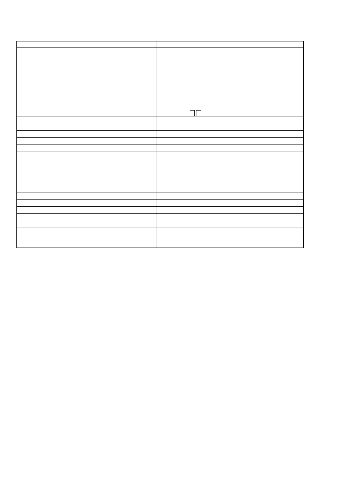
SPECIAL MENU MODE
Procedure:
1. Press the [POWER] button to turn on the main po wer , then while pressing the [TONE MODE] button, press the [A.F.D.], [2CH/A. DIRECT],
[MUSIC], [MOVIE] button in order, the message “MENU SPECIALIZED!” appears.
2. Press the M m button of the remote commander, the message “<<< SPECIAL >>>” appears.
3. Press the , button of the remote commander, the item is appears.
4. Each time the M m button of the remote commander is pressed, the item is switched in order as follows.
Some items can change the content. Display the cursor by pressing the , button of the remote commander, and changing the content
by pressing the M m button of the remote commander , and fix the content by pressing the < button of the remote commander when you
want to change the content of the item.
5. To release from this mode, while pressing the [TONE MODE] button, press the [A.F.D.], [2CH/A. DIRECT], [MUSIC], [MOVIE] button in
order again, the message “MENU SPECIALIZED OFF” appears.
Items Display Remark
Video factory menu <VIDEO FACTORY MENU> Menu mode to enter video calibration menu and DDR access check menu
If the [ENTER] button of the remote commander is pressed, entering the
menu, and operating two the following menu become possible
Video calibration V.CALIBRATION START? Procedure:
(Video factory menu) 1. “DVD” is selected by using [INPUT SELECTOR] jog.
2. Connect a color pattern generator to the COMPONENT VIDEO DVD/
BD IN jack (J6001) and DVD/BD VIDEO IN jack (J6004) on the
A_VIDEO board.
3. Input 100% color bars signal from the color pattern generator.
4. Menu that measures individual difference of hardness by automatic
operation in pressing the [ENTER] button of the remote commander, and
corrects reference value.
In a measurement once, only one of NTSC/PAL/HD can be measured
”Check XXXX V-IN” at display:
Video signal necessary for the measurement while measuring it last time
was not detected and it became an error
Confirm the input of the video of the terminal connection etc. , and
measure the [ENTER] button of the remote commander again pressing
DDR access check DDR CHECK [XX] sec XX: Time to do access check on DDR (for design evaluation)
(Video factory menu)
Auto cal mic test SPEAKER OUT [XXXXX] XXXXX: Selection of speaker output audio
[SOURCE]: nomally mode, [MIC]: mode that output audio from mic from
speaker
FL display fonts test FL FONT [0x ** = X] **: 20 to FE, X: character
FL display test ALL ON Each time DISPLAY button to change as follows
all on t test pattern 1 t test pattern 2 t all off t all on
HDCP key read HDCP KEY READ [XXX] XXX: ON or OFF
DSP SRAM check <DSP SRAM CHECK> XX: OK or NG
[ENTER] button of the remote OK: success access SRAM, NG: fail access to SRAM
r
commander
SRAM1 [XX] SRAM2 [XX]
Model version display ##### *** vX. XX @@@@ #####: Model
***: Destination
X.XX: System controller software version
@@@@: Sum value of flash memory in the system controller
Video Ucom version display Video Ucom Ver X. XX X.XX: Video system controller software version
FAROUDJA version display FAROUDJA Ver X. XX X.XX: Video Processor software version
DSP Ucom version display DSP Ucom Ver X. XX X.XX: DSP controller version
DSP serial flash version display DSP SFLASH Ver X. XX X.XX: Serial flash software version
DSP parallel flash version display DSP PFLASH Ver X. XX X.XX: DSP parallel flash version
DSP Version display DSP Ver S: ***, P: XXX ***: DSP decoder patch version, XXX: DSP post process version
DSP halt DSP HALT [XXX] XXX: ON or OFF
DSP RAM [*****]=XXXXXXXX Mode that refers to internal RAM of DSP (for design evaluation)
21
STR-DA4300ES
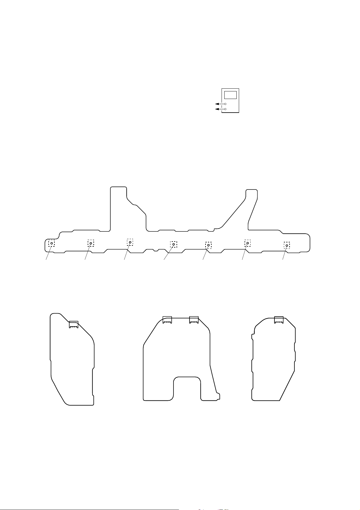
Items Display Remark
Super reset SUPER RESET [XXX] Not used for the servicing
If super reset is performed, “up convert signal level adjustment” will also be
initialized
When EEPROM initialization is required, perform the “memory clearing
mode”
RAM watch menu XXX XXX: For monitor of various internal RAM (for design evaluation)
EERROM debug EEPROM [****] [XX] ****: EEPROM address, XX: EEPROM data
Protector on/off PROTECTOR ON/OFF [XXX] XXX: ON or OFF
Model/destination change MODEL [##### * * * *] X X #####: Model, ****: Destination, XX: At or fx
Audio swap SWAP [XXXXXXXXXXX] Switching with M m button of the remote commander
Decoder select DECODER SEL [XXXX] XXXX: AUTO, LEGACY, DDPLUS, TRUEHD, DTSEXP, MP3SUR (for
debug)
Volume value display (FL/FR) FL**** FR XXXX ****: Front L-ch volume value, XXXX: Front R-ch volume value
Volume value display (SL/SR) SL**** SR XXXX ****: Surround L-ch volume value, XXXX: Surround R-ch volume value
Volume value display (CT/SW) CT**** SW XXXX ****: Center volume value, XXXX: Sub woofer volume value
Volume value display (SBL/SBR) SBL**** SBR XXXX ****: Surround back L-ch volume value, XXXX: Surround back R-ch
volume value
DAC mute information disclosure 1DAC MUTE U XXXXXXXX Display of module information to demand muting in system controller (for
design evaluation)
DAC mute information disclosure 2DAC MUTE L XXXXXXXX Display of module information to demand muting in system controller (for
design evaluation)
2nd volume value display 2nd VOLUME XXX XXX: 2nd room volume value (00 to ∞)
FL display duty change DARK OUT DUTY [XXX%] XXX: Duty value of FL display (0% to 100%)
DMPORT debug DMP KEY DEBUG [XXX] XXX: ON or OFF (for debug)
Bus overflow debug HA link OVERFLOW HAL R [XX] XX: Counter of overflow receive buffer
(receive)
Bus overflow debug HA link OVERFLOW HAL S [XX] XX: Counter of overflow transmit buffer
(transmit)
Bus overflow debug DMPORT OVERFLOW CLA [XX] XX: Counter of overflow CLA transmit buffer
22
SECTION 5
ELECTRICAL ADJUSTMENTS
BIAS ALIGNMENT ADJUSTMENT
Note: Afer 10 minutes or more have passed since the power supply was
turned on, this adjustment is done.
Connection:
STR-DA4300ES
digital voltmeter
CN1561 (CN1611, CN1761, CN1861) pin
CN1561 (CN1611, CN1761, CN1861) pin 2, CN1561 (CN1761, CN1861) pin
1
, CN1561 (CN1761, CN1861) pin
Procedure:
1. Connect a digital voltmeter to the CN1561 (CN1611, CN1761,
CN1861).
2. Press the [POWER] button to turn on the main power.
3. Adjust the RV1501 (RV1551, RV1601, RV1701, RV1751,
RV1801, R V1851) so that the digital voltmeter reading is 5 mV
to 20 mV.
Adjustment and Connection Location:
– BIAS Board (Conductor Side) –
Adjustment hole
for RV1801
(SBL)
Adjustment hole
for RV1851
(SBR)
Adjustment hole
for RV1601
(CENTER)
Adjustment hole
for RV1501
(F-L)
Adjustment hole
3
4
for RV1551
(F-R)
+
–
Adjustment hole
for RV1701
(SUR-L)
Adjustment hole
for RV1751
(SUR-R)
– PROTECTOR (SB) Board
(Component Side) –
CN1861
4
1
– PROTECTOR (F-C) Board
(Component Side) –
CN1611
4
CN1561
1
1
4
– PROTECTOR (SURR) Board
(Component Side) –
CN1761
1
4
23

STR-DA4300ES
)
VIDEO CALIBRATION ADJUSTMENT
Adjustment to decide the standard of the video input signal.
Note: After replacing D_VIDEO board, or after “SUPER RESET” of the
special menu mode is executed, perform this adjustment.
Connection:
color pattern
generator
color bars 100%
A_VIDEO board COMPONENT VIDEO DVD/BD IN jack (J6001
DVD/BD VIDEO IN jack (J6004)
Procedure:
1. “DVD” is selected by using [INPUT SELECTOR] jog.
2. Connect a color pattern generator to the COMPONENT
VIDEO DVD/BD IN jack (J6001) on the A_VIDEO board
and DVD/BD VIDEO IN jack (J6004) on the A_VIDEO board.
3. Input NTSC color bars signal from the color pattern generator.
4. Press the [POWER] button to turn off the main power
5. While pressing the [MEMORY/ENTER], [MUSIC] and
[DMPORT] buttons, press the [POWER] button to turn on the
main power. It enters the test mode, and display as below.
V.CALIBRATION START? y NTSC : MW--_____
set
(PAL input) PAL : MW--_____
(HD input) HD-V : MW--_____
FM AUTO STOP CHECK
signal
generator
set
Procedure:
1. Turn on the set.
2. Input the following signal from signal generator to FM antenna
input directly.
Carrier frequency: A = 87.5 MHz, B = 98 MHz, C = 108 MHz
Deviation : 75 kHz
Modulation : 1 kHz
ANT input : 35 dBu (EMF)
Note: Use 75 ohm coaxial cable to connect signal generator and the set.
You cannot use video cable for checking.
Use signal generator whose output impedance is 75 ohm.
3. Set to FM tuner function and scan the input FM signal with
automatic scanning.
4. Confirm that input frequency of A, B and C are detected and
automatic scanning stops.
When the station signal is received in good condition, automatic
scanning stops.
6. In state of step 5, press the [MEMORY/ENTER] button. The
adjustment is automatically completed, and result is written
in the EEPROM, and display as below.
(NTSC input) NTSC : MW OK C_V__
(PAL input) PAL : MW OK C_V__
(HD input) HD-V : MW OK C_V__
When “Check XXXX V-IN” is displayed, Video signal
necessary for the measurement while measuring it last time
was not detected and it became an error . Confirm the input of
the video of the terminal connection etc., and measure the
[MEMORY/ENTER] button again pressing.
7. Input PAL color bars signal from the color pattern generator.
8. Perform step 4 to 6.
9. Input HD color bars signal (720p or 1080p) from the color
pattern generator.
10. Perform step 4 to 6.
11. When all the adjustments end, display as below.
V.CAL COMPLETE N:P:H
24
SECTION 6
DIAGRAMS
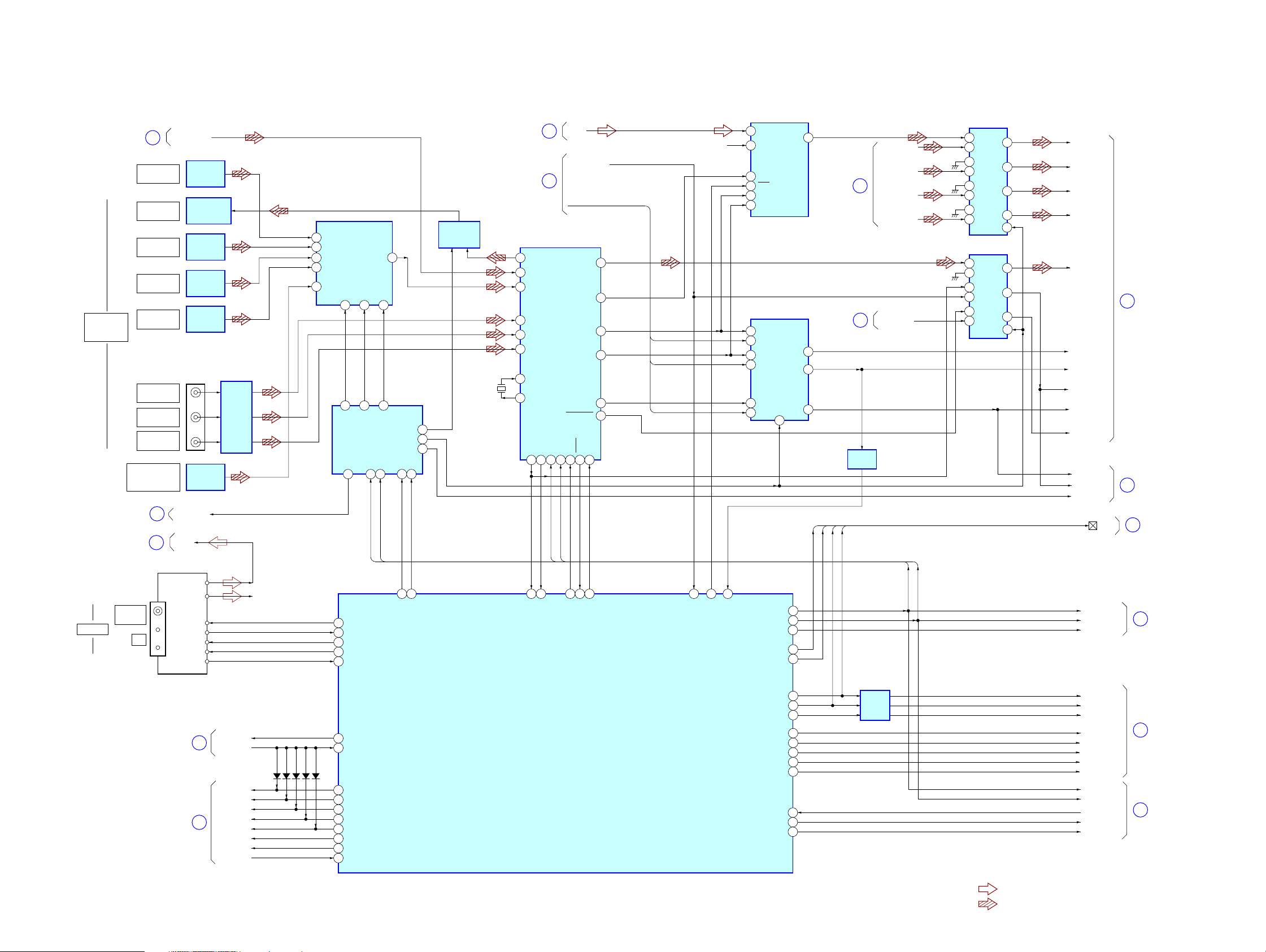
6-1. BLOCK DIAGRAM – CONTROL Section –
STR-DA4300ES
DIGITAL
ASSIGNABLE
(INPUT ONLY)
ANTENNA
(Page 28)
PORTABLE AV IN
(Page 28)
(Page 30)
FM 75Ω
COAXIAL
1
TV
OPTICAL IN
MD/DAT
OPTICAL OUT
MD/DAT
OPTICAL IN
VIDEO 1
OPTICAL IN
SAT/CATV
OPTICAL IN
VIDEO 2
COAXIAL IN
DVD/BD
COAXIAL IIN
SA-CD/CD
COAXIAL IIN
VIDEO 3 IN/
DIGITAL (OPT)
2
3
TUNER (FM/AM)
AM
HDMI_SPDIF
OPTICAL
RECEIVER
IC2225
OPTICAL
TRANSCEIVER
IC2205
OPTICAL
RECEIVER
IC2204
OPTICAL
RECEIVER
IC2201
OPTICAL
RECEIVER
IC2202
J2201
WAVE
SHAPER
IC2209
OPTICAL
RECEIVER
IC707
XM/H_SEL
TU-L
TUN_L
TUN_R R-CH
TUN_DAT
TUN_DO
TUN_CLK
TUN_CE
TUN_TUNED
14 D5
4D0
1D3
3D1
15 D4
INPUT
SELECTOR
IC2207
A1
A0
10
11
5
4
DSEL1
DSEL06DSEL2
H_SEL1
S-IN
2
14
COM1-DAT
60 TUNER_DATA
71 TUN_DO
61 TUNER_CLK
70 TUN_LAT
69 TUN_TUNED
5Y
A2
9
DATA DECODER
CLK12LAT13OE
11
COM1-CLK
109
IC2210
REQ
7
15DSP_SEL
1ANA/DIGI
108
D595_OE
D595_LAT
DIGITAL OUT
SWITCH
IC2206
24.576MHz
X2201
(Page 30)
(Page 28)
DIGITAL AUDIO INTERFACE RECEIVER
1 RXOUT
10 RX6/UI
2 RX0
8 RX4
5 RX3
4 RX2
XIN
29
XOUT28
67
6
7
IC2208
RERR
DI
38
37DO36
COM1-DAT
66
DIR_DO
DIR_RERR
2CH-L
HDMI_ERROR
HDMI_BCK, HDMI_LRCK,
HDMI_MCK
CE
CKST
CL
40
39
34
41
COM1-CLK
65
68
64
DIR_CE
DIR_CKST
21RDATA
27XMCK
17RBCK
20RLRCK
16RMCK
33AUDIO/VO
XMODE
DIR_XMODE
HDMI_BCK
HDMI_LRCK
HDMI_MCK
R-CH
93
46
AD_RST
HDMI_ERROR
168
FSRATE1
A/D CONVERTER
IC2217
10
AINL
12
AINR
2
MCLK
9
RST
7
SCLK
8
LRCK
DATA SELECTOR
IC2212
14
A3
13
B3
11
A2
10
B2
5
A1
S
6
B1
1
COM1_DATA 111
COM1_CLK 110
V595_LAT 8
V595_OE 7
SDOUT
10XM_DA_LAT
Y3
Y2
Y1
4
(Page 28)
(Page 29)
12
9
7
V595 OE
V595 LAT
COM2-CLK
COM2-DAT
8
15
BUFFER
IC2211
HDMI_DATA2
HDMI_DATA3
HDMI_DATA4
NON_LPCM
COM1-CLK
COM1-DAT
DATA SELECTOR
IC2213
2
A0
Y0
3 B0HDMI_DATA1
5A1
6 B1
11 A2
10 B2
14 A3
13 B3
S
DATA SELECTOR
IC2214
2
A0
Y0
3 B0
5A1
Y1
6 B1
11 A2
Y2
10 B2
S
4
1
4
7
9
1
SI_B
SI_CY1 7
SI_DY2 9
SI_EY3 12
SI_A
BCK
LRCK
DIR-ERR
MCK
DIR_NONAU
D/A MCK
ERR
ANA/DIGI
COM1_DATA
COM1_CLK
XM_DACLAT
CTL
9
10
11
(Page 26)
(Page 27)
(Page 33)
(Page 33)
12
STR-DA4300ES
(Page 34)
(Page 31)
4
5
4/8_RY
PROTECTOR
SP-A-RY
SP-B-RY
REAR-RY
SB-RY
C-RY
PREOUT-RY
HP-RY
HPSW
D1007
D1008
D1010
D1011
D1009
87
163
81
83
86
85
84
76
79
23
4/8_RY
PROTECTOR
SP-A_RY
SP-B_RY
SR_RY
SB_RY
C_RY
PREOUT_RY
HP_RY
HP_IN
SYSTEM CONTROLLER
IC2003 (1/3)
COM2_DATA
COM2_CLK 112
FUNC_LAT 91
MIC_ON 26
EVOL_DAT
EVOL_CLK 105
2ND_RY 106
BRAVIA_SEL
113
92
107
95DA_DO
94DA_LAT
96DA_RST
BUFFER
IC2011
(1/2)
AUCOM-DATA
AUCOM-CLK
FUNC-LAT
MIC
EVOL_DATA
EVOL_CLK
2ND-RY
BRAVIA_SEL
COM1_DATA
COM1_CLK
DA DO
DA LAT
DA RESET
13
14
(Page 30)
(Page 27)
• R-CH is omitted due to same as L-CH.
• SIGNAL PATH
: AUDIO (ANALOG)
: AUDIO (DIGITAL)
2525
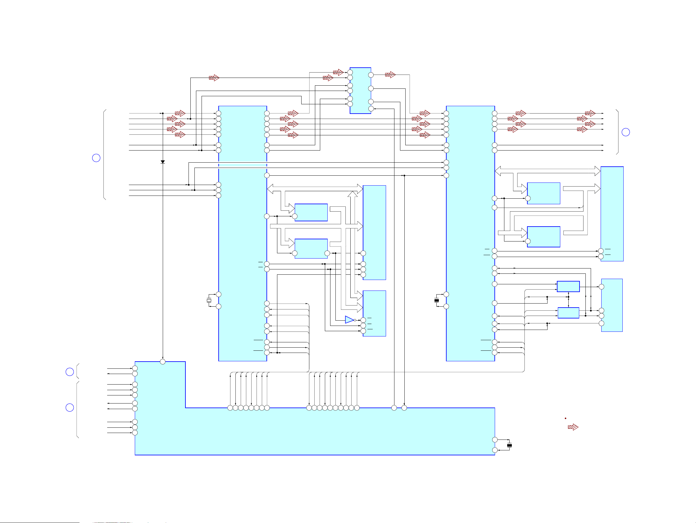
STR-DA4300ES
6-2. BLOCK DIAGRAM – DSP Section –
(Page 25)
(Page 27)
(Page 27)
16
17
9
D232C_RX
D232C_TX
MD_DATA
MD_BUSY
MD_INT
DM_DATA
DM_BUSY
MD2
DRST_TRG
DUCOM_RESET
SI_A
SI_B
SI_C
SI_D
SI_E
BCK
LRCK
DIR-ERR
MCK
DIR_NONAU
102
103
89
63
82
90
64
52
36
55
SI3
SO3
MD_DATA
MD_BUSY
MD_INT
DM_DATA
DM_BUSY
MD2
DRST_TRG
XRESET
1
RDATA0
D5001
X5001
12.288MHz
P14
M13
M14
L14
K14
G14
H13
F1
F14
F13
B4
A2
DPSIA
DPSIB
DPSIC
DPSID
DPSIE
DPBCK
DPLRCK
FLAG1
DPFSCK
NONAUDIO
CLKIN
XTAL
DSP1_MOSI
93
92
DSP1_MOSI
DSP1
IC5002
DPDVLRCK
AD8 – AD15
BOOTCFG0
BOOTCFG1
DSP1_MISO
DSP1_SPIDS
DSP1_SPICLK
94
11
DSP1_MISO
DSP1_SPIDS
DSP1_SPICLK
DPSOA
DPSOB
DPSOC
DPSOD
DPSOE
DPDVBCK
P_ERROR
AD0 – AD7
ALE
WR
RD
MISO
MOSI
SPICLK
SPIDS
FLAG0
RESET
DSP1_INT
DSP1_RESET
83
12
DSP1_INT
DSP1_RESET
P10
P11
P12
P13
N14
H14
J14
E14
N2
M2
N3
A10
A9
B9
DSP1_BOOTCFG0
C2
DSP1_BOOTCFG1
C1
A11
F2
B10
DSP1_BOOTCFG0
DSP1_BOOTCFG1
13
14
DSP1_BOOTCFG0
DSP1_BOOTCFG1
ADDRESS LATCH
D0 – D7
11
LE
ADDRESS LATCH
D0 – D6
11
LE
DSP1_MISO
DSP1_MOSI
DSP1_SPICLK
DSP1_SPIDS
DSP1_INT
DSP1_RESET
IC5009
O0 – O7
IC5010
O0 – O4
O6
DSP2_MOSI
SF2_CPU_CE
SF2_DSP2_MAS
17
20
100
99
DSP2_MOSI
SF2_CPU_CE
SF2_DSP2_MAS
DATA SELECTOR
IC5013
11
3A
10 3B
21A
3 1B
52A
6 2B
SELECT
13 26
IC5012
DSP2_INT
DSP2_MISO
DSP2_SPIDS
DSP2_RESET
DSP2_SPICLK
101
DSP2_MISO
DSP2_SPICLK
21
84
22
DSP2_INT
DSP2_SPIDS
DSP2_BOOTCFG0
DSP2_BOOTCFG1
25
26
DSP2_RESET
DSP2_BOOTCFG0
9
3Y
1Y
4
7
2Y
1
FLASH MEMORY
IC5006
DQ0 – DQ7
DQ15/A-1,
A0 – A19
CE#
11
WE#
28
OE#
12
RESET#
S-RAM
IC5007
I/O0 – I/O7
A0 – A18
8
CE
37
OE
15
WE
DSP2_BOOTCFG1
9
10
P_ERROR
DSP2_SIB_SEL
X5201
25MHz
DSP CONTROLLER
IC5208
M13
M14
L14
K14
P14
G14
H13
F1
F14
F13
B4
A2
DPSIB
DPSIC
DPSID
DPSIE
DPSIA
DPBCK
DPLRCK
FLAG1
DPFSCK
P_ERROR
CLKIN
XTAL
DSP2
IC5202
DPSOA
DPSOB
DPSOC
DPSOD
DPDVBCK
DPDVLRCK
AD0 – AD7
DAI_P1
AD8 – AD15
SPICLK
MOSI
SF2_DSP2_CE
SF2_DSP2_MAS
BOOTCFG0
BOOTCFG1
MISO
SPIDS
FLAG0
RESET
XOUT
ALE
RD
WR
N2
P15
N3
M2
B9
A9
E14
P9
A10
XIN
P10
P11
P12
P13
H14
J14
DSP2_BOOTCFG0
C2
DSP2_BOOTCFG1
C1
DSP2_SPIDS
A11
DSP2_INT
F2
DSP2_RESET
B10
X5202
12.5MHz
57
58
ADDRESS LATCH
IC5209
D0 – D7
11
LE
ADDRESS LATCH
IC5210
D0 – D7
11
LE
SF2_CPU_CE
SF2_DSP2_MAS
DSP2_SPICLK
DSP2_MOSI
DSP2_MISO
O0 – O7
O0 – O7
DSP1_A16
FLIP-FLOP
IC5212
BUFFER
IC5211
SIGNAL PATH
SDO1
SDO2
SDO3
SDO4
BCK
LRCK
S-RAM
IC5207
I/O0 – I/O7
A0 – A16
41
OE
17
WE
SERIAL FLASH
IC5213
1
CE#
6
SCK
5
SI
2
SO
: AUDIO (DIGITAL)
18
(Page 27)
STR-DA4300ES
2626
6-3. BLOCK DIAGRAM – DIGITAL AUDIO Section –
STR-DA4300ES
(Page 33)
(Page 28)
(Page 34)
(Page 29)
(Page 33)
(Page 34)
(Page 33)
(Page 26)
19
20
21
22
23
24
25
17
DMPORT_TX
DMPORT_RX
DMPORT_DET
CEC_TX
CEC_RX
POW-RY
STOP
STOP
GUI_TX
GUI_RX
GUI_BUSY
GUI_MD
GUI_FLG
GUI_RST
XM_UART_TX
XM_UART_RX
XM RESET
XM POW
SIRIUS_RX
SIRIUS_TX
SI_POW_EN
MD_DATA
MD_BUSY
MD_INT
DM_DATA
DM_BUSY
DRST_TRG
DUCOM_RESET
(Page 26)
MD2
SD01
SD02
SD03
SD04
18
154
DMUART_DM/M
155
DMUART_M/DM
156
DMPORT_DET
47
CEC_M/DV
121
CEC_DV/M
75
POWER RY2
82
STOP
140
VIDEO-UCOM_VM/M
141
VIDEO-UCOM_M/VM
142
VIDEO-UCOM_BUSY
124
VIDEO-UCOM_MODE
125
VIDEO-UCOM_END-FLAG
136
VIDEO-UCOM_RESET
137
XM_XM/M
138
XM_M/XM
139
XM_RESET
3
XM_POW
148
SIRIUS_TX
149
SIRIUS_RX
77
SIRIUS-POW_EN
144
M-D_DATA
51
MD_BUSY
54
M-D_INT
143
D-M_DATA
52
DM_BUSY
50
DSP-UCOM_MODE
49
DSP-UCOM_END-FLAG
53
DSP-UCOM_RESET
BCK
LRCK
EEPROM_SDA
EEPROM_SCL
LIP SYNC ADJUST
4
DIA
DIB
5
6
DIC
DID
7
3
BCKI
MCKI
2
IC2223
DOA
DOB
DOC
DOD
DQ0 – DQ15
A0 – A10, BA
WEN
CSN
CASN
RASN
DQM
CLKO
CKE
SCLK
DMUTEN
RSTN
SIO
XCS
19
20
21
22
DQ1 – DQ16
A0 – A11
43
40
42
41
31
30
29
SI
10
9
14
15
11
8
WE
15
CS
18
CAS
16
RAS
17
UDQM
36
LDQM
14
CLK
35
CKE
34
SD-RAM
IC2224
(Page 25)
DA DO
COM1_DATA
14
D/A CONVERTER
45 DATA1
46 DATA2
47 DATA3
31 DATA4
40 BCK
41 LRCK
38 SCKI
33 MDO
34 MDI
35 MCCOM1_CLK
36 MLDA LAT
37 RSTDA RESET
IC2218
14VOUT1
13VOUT2
12VOUT3
11VOUT4
16VOUT7
20VOUT8
10VOUT5
9VOUT6
LOW-PASS
FILTER
IC2222
LOW-PASS
FILTER
IC2221
LOW-PASS
FILTER
IC2219
LOW-PASS
FILTER
IC2220
R-CH
R-CH
R-CH
D/A-L
D/A-SL
D/A-SBL
D/A-C
D/A-SW
26
(Page 30)
• R-CH is omitted due to same as L-CH.
• SIGNAL PATH
: AUDIO (ANALOG)
D/A MCK
(Page 25)
IC2004
10
131
INITX
RS232C_MOUT
RS232C_MIN
232C-SEL1
232C-SEL2
MD2
D232C_RX
DATA SELECTOR
IC2010
2Y
9
4
1C1
1C2
5
166
167
135
134
128
BUFFER
IC2009
7
1Y
11
2C1
12
2C2
10
2C0
B
2A14
LEVEL SHIFT
IC2002
D232C_TX
RX232C
TX232C
RS-232C DRIVER
IC881
12
R1OUT
11
T1IN
R1IN
T1OUT
BUFFER
IC2216
EEPROM
IC2007
174
5
175
40
X1
39
X0
SDA
6
SCL
X2001
4MHz
SYSTEM CONTROLLER
IC2003 (2/3)
170
FSRATE2
625655
AVSYNC_SIO
AVSYNC_XCS
SYSTEM MUTING
AVSYNC_RSTN
SWICTH
Q2205, 2206
59
MUTE
STB +3.3V
RESET SIGNAL
GENERATOR
RESET SIGNAL
IC2005
BUFFER
IC2006
126
ERR
ANA/DIGI
RESET SWITCH
RST_TRG
: AUDIO (DIGITAL)
16
(Page 26)
(Page 29)
27
13
14
2
3
J881
RS-232C
STR-DA4300ES
2727
STR-DA4300ES
6-4. BLOCK DIAGRAM – HDMI Section –
CN3501
HDMI
ASSIGNABLE
(INPUT ONLY)
IN 3
CN3502
HDMI
ASSIGNABLE
(INPUT ONLY)
IN 2
CN3503
HDMI
ASSIGNABLE
(INPUT ONLY)
IN 1
DATA0+
DATA0–
DATA1+
DATA1–
DATA2+
DATA2–
CLOCK+
CLOCK–
SDA (5V)
SCL (5V)
HOT PLUG DET
+5V POWER
CEC
DATA0+
DATA0–
DATA1+
DATA1–
DATA2+
DATA2–
CLOCK+
CLOCK–
SDA (5V)
SCL (5V)
HOT PLUG DET
+5V POWER
CEC
DATA0+
DATA0–
DATA1+
DATA1–
DATA2+
DATA2–
CLOCK+
CLOCK–
SDA (5V)
SCL (5V)
HOT PLUG DET
+5V POWER
CEC
• SIGNAL PATH
7
9
4
6
1
3
10
12
16
15
19
18
13
7
9
4
6
1
3
10
12
16
15
19
18
13
7
9
4
6
1
3
10
12
16
15
19
18
13
: AUDIO (DIGITAL)
: VIDEO
LEVER SHIFT
Q3501
3
GATE
IC3524(1/3)
LEVER SHIFT
Q3502
11
GATE
IC3524(2/3)
LEVER SHIFT
Q3503
8
GATE
IC3524(3/3)
Q [4 – 11, 16 – 23, 28 – 35]
SWITCH
TX_INT
TX_RST
30
123
TX_RST
ODCK, HSYNC, VSYNC, DE
SPDIF
WS
XMFS
MCK
XM256FS
SCK
XM64FS
SD0
XMDATA
SD1
SD2
SD3
TX_INT
R0X0+
22
R0X0-
21
25
R0X1+
R0X1-
24
28
R0X2+
R0X2-
27
R0XC+
19
R0XC-
18
DSDA0
30
DSCL0
31
2
1
12
13
9
10
HPD0
16
RPWR0
32
42
R1X0+
R1X0-
41
45
44
48
47
39
38
50
51
36
52
62
61
65
64
68
67
59
58
70
71
56
72
HDMI INPUT
R1X1+
R1X1-
R1X2+
R1X2-
R1XC+
R1XC-
DSDA1
DSCL1
HPD1
RPWR1
R2X0+
R2X0-
R2X1+
R2X1-
R2X2+
R2X2-
R2XC+
R2XC-
DSDA2
DSCL2
HPD2
RPWR2
TX0+
TX0-
TX1+
TX1-
TX2+
TX2-
TXC+
TXC-
SELECT
IC3503
TPWR/I2CADDR
HPDIN
RESET#
TSDA
TSCL
LSDA/EPSEL[0]
LSCL/EPSEL[1]
7
8
4
5
1
2
10
11
79
76
13
77
78
14
15
9185_HPD[1]
9185_RST[1]
9185_RST[1]
9185_HPD[1]
93 94
9185 1 RST
9185 1 HPD1-3
117
118
UC3V_SCL
X3501
28.322MHz
UC3V_SDA
UC3V_SDA
UC3V_SCL
44
R0X0+
43
R0X0–
48
R0X1+
47
R0X1–
52
R0X2+
51
R0X2–
40
R0XC+
39
R0XC–
HDMI RECEIVER
94
XTALOUT
95
XTALIN
35
R0PWR5V
DSDA0
33
DSCL0
34
CSDA
26
CSCL
27
DATA SELECTOR
IC3508
2Y1
5
2Y0
1
1Y1
14
1Y0
12
IC3511
2-COM
1-COM
A
10
8
EDID SEL0
Q0 – Q35
ODCK
HSYNC
VSYNC
SPDIF
SD0 -SD3
MCLK
SCK
WS
MUTE
RESET
INT
3
13
16 -13,10 -7,3 -1,
129 -126,123 -120,
144,141 -138,135 -132,
5
20
21
DE
19
78
81 -84
89
86
85
67
89
91
EEPROM
IC3509
5
SDA
6
SCL
WP
Q[28]-Q[35]
Q[16] -Q[23],
Q [4] - Q [11],
36
117 -114,111 -108
4
BUFFER
IC3855
SPDIFWSMCK
SCK
SD0 -SD3
RESET
RX_INT
7
ODCK
RESET
35
RX_RST
HSYNC
RX_INT
121
RX_INT
DE
VSYNC
98
168
V.SYNC_DET
98 -90, 86 -77
88
2
3
1
21
4
4
9 – 6
4
17 – 20
15
16
5
11
10
VIDEO SYSTEM CONTROLLER
AUDIO MUTE REQ
D0 -D35
75 -67, 63 -56
IDCK
HSYNC
VSYNC
DE
HDMI
TRANSCEIVER
IC3513
DL2
SPDIF
SD0 -SD3
DL0, DR1,
DL1, DR2
DCLK
DR0
MCLK
SCK
WS
IC3610 (1/2)
TX0+
34
TX0–
33
TX1+
37
TX1–
36
TX2+
40
TX2–
39
TXC+
31
TXC–
30
DSDA
47
DSCL
46
HPD
51 19
CEC DATA
Q2001 – 2004
24
25
49
48
TX_INT
TX_RST
UC3V_SDA
UC3V_SCL
INT
RESET#
CSDA
CSCL
(Page 29)
28
DATA0+
7
DATA0–
9
DATA1+
4
DATA1–
6
DATA2+
1
DATA2–
3
CLOCK+
10
CLOCK–
12
16
SDA (5V)
15
SCL (5V)
HOT PLUG DET
13
CEC
HDMI/XM SELECTOR
IC2228
A0
2
3B0
5A1
6B1
11 A2
10 B2
14 A3
13 B3
HDMI/XM SELECTOR
2
3B0
5A1
6B1
11 A2
10
14 A3
13
31TX 5VPWR
A0
B2
B3
S
1
IC2231
S
7
Y0
Y2
Y3 12
Y0
Y2
Y3 12
ASSIGNABLE
(INPUT ONLY)
4
7Y1
9
4
7Y1
9
CN3511
HDMI
OUT
LEVEL SHIFT
IC2227
CEC_TX
CEC_RX
UC3V_SDA,
UC3V_SCL
XMDATA, XMFS,
XM256FS, XM64FS
HDMI_SPDIF
HDMI_LRCK
HDMI_MCK
HDMI_BCK
HDMI_ERROR
HDMI_DATA1
HDMI_DATA2
HDMI_DATA3
HDMI_DATA4
XM/H_SEL
TX_5VPWR
20
(Page 27)
29
(Page 29)
30
(Page 33)
1
(Page 25)
7
(Page 25)
8
(Page 25)
2
(Page 25)
31
(Page 34)
STR-DA4300ES
2828
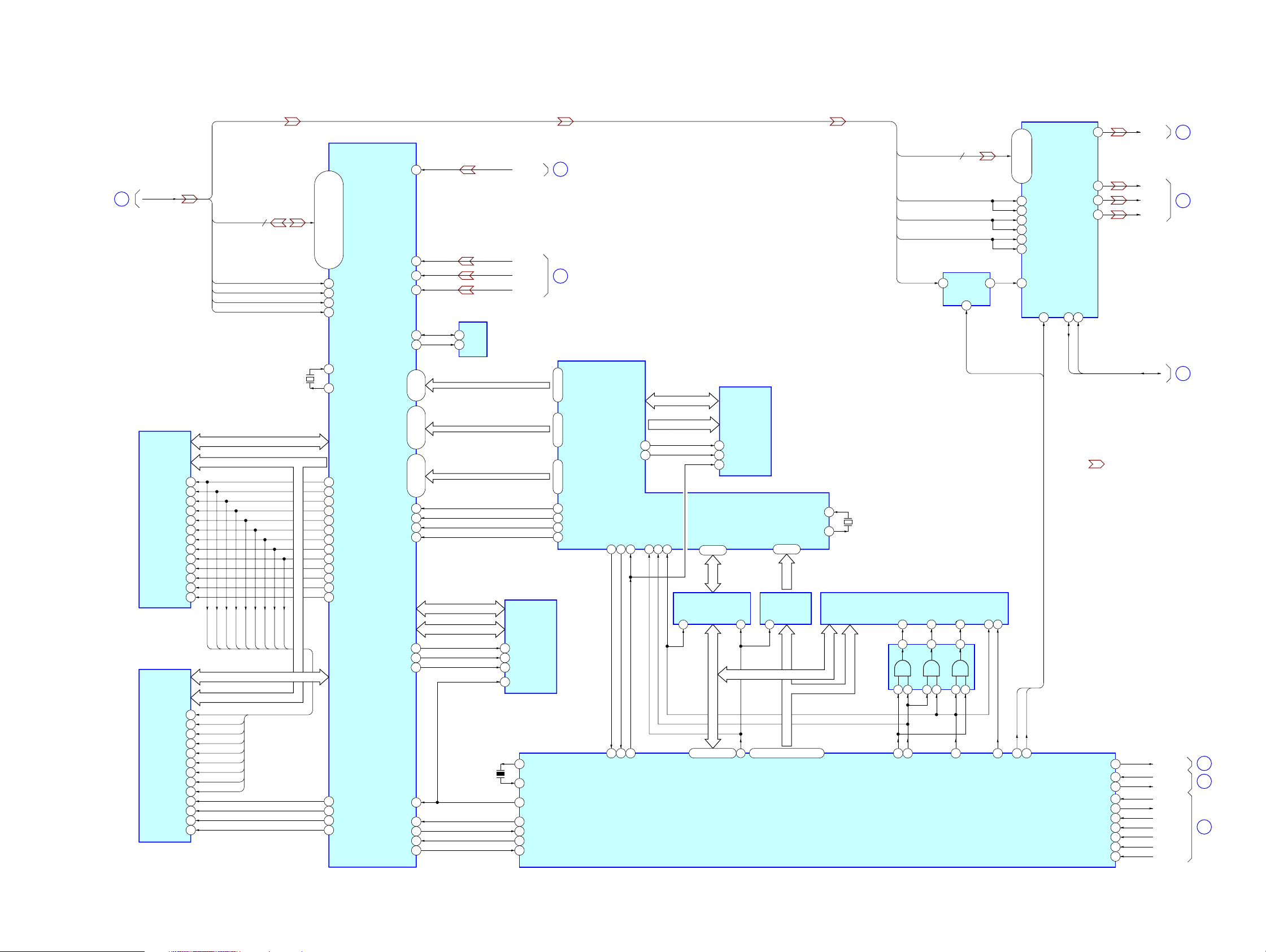
6-5. BLOCK DIAGRAM – VIDEO PROCESS Section –
VIDEO PROCESSOR
Q [4 – 11, 16 – 23,
28 – 35],
ODCK, HSYNC,
(Page 28)
28
VSYNC, DE
SD-RAM
IC3618
DQ0 – DQ15
A0 – A12
UDQS
SD-RAM
IC3602
DQ0 – DQ15
A0 – A12
UDQS
CLK
/CLK
CKE
BA0
BA1
RAS
CAS
WE
LDM
UDM
LDQS
CLK
/CLK
CKE
BA0
BA1
RAS
CAS
WE
LDM
UDM
LDQS
45
46
44
26
27
24
CS
23
22
21
20
47
16
51
45
46
44
26
27
CS
24
23
22
21
20
47
16
Q [4 – 11,
16 – 23,
28 – 35]
ODCK
HSYNC
VSYNC
DE
FSDATA [16] – FSDATA [31]
FSADD [0] – FSADD [12]
CLKP
CLKN
CKE
FSDATA [0] – FSDATA [15]
FSADD [0] – FSADD [12]
CLKP
CLKN
CKE
FSBKSEL0
FSBKSEL1
FSCS0
RAS
CAS
WE
24
DATA BUS
ADDRESS BUS
FSBKSEL0
FSBKSEL1
FSCS0
DATA BUS
ADDRESS BUS
RAS
X3603
19.6MHz
CAS
WE
PD0 – PD23
F23 – F26, E23, E24
L23 – L26, N23 – N26,
K23 – K26, J23, J24, G23 –G26,
DCLK
P24
DHS
P25
DVS
R26
DEN
P26
C26
TCLK
B26
XTAL
FSCLKP
D5
FSCLKN
C5
FSCKE
C4
FSBKSEL0
C21
FSBKSEL1
C20
FSCS0
D21
FSRAS
C24
FSCAS
D24
FSWE
C23
FSDQM3
B22
FSDQM2
B17
FSDQS3
A22
FSDQS2
A17
FSDQM1
A11
FSDQM0
A6
FSDQS1
B11
FSDQS0
B651
IC3601
MSTR0_SDA
MSTR0_SCL
BDATA21
BDATA16
BDATA13
BDATA8
BDATA5
BDATA0
BHREF_DE
OCMDATA0 –
OCMDATA15
OCMADDR1 –
OCMADDR21
ROM_CS_N
OCN_RE_N
OCN_WE_N
MSTR1_SCL
MSTR1_SDA
OCM_UDI_1
OCM_UDO_1
A3P
C1P
B1P
A1P
I
I
I
IPCLK2
BHS
BVS
RESET
AF4
AC1
AC2
AB1
AA23
AA24
J1 – J3,
H1 – H3
E1, E2
G3, F1 – F3,
D2, D3,
C1 – C3, B1
M4
L3
L2
K1
AD24
AC25
AC26
AD9
A3
A2
B3
B2
EEPROM
IC3621
SDA5
6
SCL
DR0 – DR5
DG0 – DG5
DB0 – DB5
DOTCLK
HCSYNC_N
VSYNC_N
BLANK_N
F_D [0] – F_D [15]
F_A [1] – F_A [21]
X3602
4MHz
CVBS
COMP-Y
CB
CR
FLASH MEMORY
IC3615
DQ0 – DQ15
A0 – A20
CE
26
OE
28
WE
11
RESET
12
40
X1
39
X0
Faroudja UCOM RESET
126
Faroudja UCOM BUSY
142
Faroudja Power DETECT
125
Faroudja UCOM UART TX
141
Faroudja UCOM UART RX
140
32
33
111 – 116
119 – 124
127 – 132
139
137
136
138
DR0 – DR5
DG0 – DG5
DB0 – DB5
DOTCLK
HCSYNC_N
VSYNC_N
BLANK_N
(Page 32)
(Page 32)
OSD CONTROLLER
IC3604
MD0 – MD15
MA1 – MA24
MOE_N
MWE_N
WAIT_N
23
25
11922 21
YAMAHA WAIT_N
Y_D [0] – Y_D [15]
Y_A [0] – Y_A [23]
74
73
INT_N
RESET_N39CS_N28WR_N29RD_N
YAMAHA INT_N
YAMAHA RESET
DATA BUS
ADDRESS BUS
30
DIR
1
46 – 56, 59 – 63
FLASH MEMORY
IC3603
DQ0 – DQ15
A0 – A23
OE
34
WE
13
RESET
14
D0 – D7
15 – 22
YAMAHA_D [0] –
YAMAHA_D [7]
BUFFER
IC3620
XOE
19
D [8] – D [15]
DATA BUS
D [0] – D [15]
18
YAMAHA CE
SRAM IO0 – SRAM IO15/
YAMAHA D0 – YAMAHA D7
XIN
XOUT
PS0 – PS2
33 – 31
YAMAHA_A [0] –
YAMAHA_A [2]
BUFFER
IC3619
XDE
19
A [0] – A [2]A [0] – A [17]
BUS
ADDRESS
67 – 72, 75 – 83, 64 – 66
SRAM A0 – SRAM A16/
YAMAHA PS0 – YAMAHA PS2
141
142
X3601
33.2MHz
S-RAM
I/O0 –
IC3611
I/O15
A0 –
A16
AND
A [1] – A [17]
D [0] – D [15]
GATE
IC3609
VIDEO SYSTEM CONTROLLER
IC3610 (2/2)
Q [16 – 23,
28 – 35]
HSYNC
VSYNC
DE
ODCK
WE UB LB41OE
17 40 39
3
1
2
10 9812 13
26
27
SRAM LB/WE
SRAM UB/WE
16
FREQUENCY
MULTIPLIER
IC3854
2 8
IN OUT2
FSO
4
DAC_CLK_SEL
11
25
RDX
CE
6
19
SRAM CE
D/A CONVERTER
IC3850
4 – 9, 12, 13,
16 – 18, 26 – 30
Y0 – Y7, C0 – C7
23 P_HSYNC
50 S_HSYNC
24 P_VSYNC
49 S_VSYNC
25 P_BLANK
48 S_BLANK
32 CLKIN_A
RESET
33
VDAC_RESET
VDAC_RESET
DAC_CLK_SEL
32
7
DAC CLK SEL
VDAC_RESET
MAIN UCOM UART RX
MAIN UCOM UART TX
MAIN UCOM UART BUSY
V
44
Y/G
39
38
CB/R
37
CR/B
SDA21SCLK
22
UC3V_SCL
UC3V_SDA
• SIGNAL PATH
NON LPCM
Flash Update RX
Flash Update TX
STOP IN
ENDFLAG
INITX
MD2
STR-DA4300ES
: VIDEO
92
134
135
137
138
139
6
136
131
128
VOUT
Y OUT
CB OUT
CR OUT
UC3V_SDA,
UC3V_SCL
34
35
29
(Page 25)
NON_LPCM
RX232C
TX232C
GUI_RX
GUI_TX
GUI_BUSY
STOP
GUI_FLG
GUI_RST
GUI_MD
(Page 32)
(Page 32)
(Page 28)
15
27
(Page 27)
22
(Page 27)
STR-DA4300ES
2929
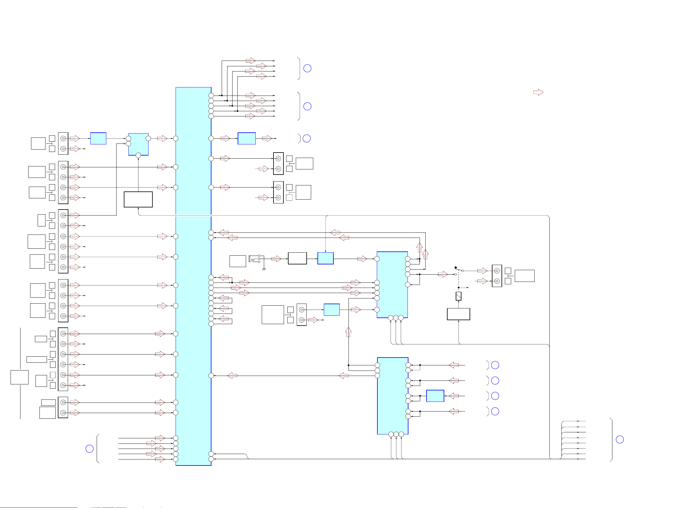
STR-DA4300ES
6-6. BLOCK DIAGRAM – ANALOG AUDIO Section –
D/A-L
D/A-C
INPUT SELECTOR
IC1003
12
X
X0
14
X1
A
10
PHONO/BRAVIA
SELECT SWITCH
Q1011, 1012
BRAVIA_SEL
13
MULTI
CHANNEL
INPUT
PHONO
IN
SA-CD/CD
IN
MD/TAPE
IN
TV
IN
SAT/CATV
AUDIO
IN
DVD/BD
AUDIO
IN
VIDEO 2
AUDIO
IN
VIDEO 1
AUDIO
IN
FRONT
SURROUND
SUR
BACK
CENTER
SUB
WOOFER
L
R
J1002 (1/2)
L
R
L
R
L
R
L
R
L
R
J1004 (1/2)
L
R
L
R
L
R
L
R
L
R
J1001
J1003
J1006
J1007
(Page 27)
R-CH
R-CH
R-CH
R-CH
R-CH
R-CH
R-CH
R-CH
R-CH
R-CH
R-CH
26
EQ AMP
IC1006
D/A-SL
D/A-SBL
D/A-SW
INPUT SELECTOR,
ELECTRICAL VOLUME
IC1001
34 INL7
32 INL6
30 INL5
28 INL4
26 INL3
24 INL2
22 INL1
10 LIN1
13 SLIN1
15 SBLIN1
12 CIN1
17 SWIN1
49 LIN2
52 SLIN2
54 SBLIN2
51 CIN2
56 SWIN2
SBLVIN
INL9
LVIN
FRONT-L
SL
SBL
C
36
(Page 31)
• R-CH is omitted due to same as L-CH.
• SIGNAL PATH
: AUDIO (ANALOG)
2ND-RY
BRAVIA_SEL
MIC
EVOL_DATA
EVOL_CLK
DATA
CLK
LAT-F
2ND-RY
BRAVIA_SEL
MIC
EVOL_DATA
EVOL_CLK
AUCOM-DATA
AUCOM-CLK
FUNC-LAT
13
(Page 25)
J1002 (2/2)
J1004 (2/2)
VIDEO 3 IN/
PORTABLE
AV IN
AUDIO
L PREOUT
SL PREOUT
SBL PREOUT
C PREOUT
W PREOUT
2CH-L
L
R
L
R
LINE AMP
L
R
MD/TAPE
OUT
VIDEO 1
AUDIO
OUT
Q708
J703 (1/2)
37
6
(Page 31)
(Page 25)
MIC
MIC AMP
IC703
BUFFER
IC706
R-CH
INPUT SELECTOR
IC1002
3L2
8L5
9L6
5L3
6L4
2L1
DATA
17 16 14
DATA
INPUT SELECTOR
IC8009
12
L_COM3
9
L_COM2
6 L_COM1
DATACKST
17 16 14
DATA
CLK
CLK
CK
ST
LAT-F
L1
LAT-F
10L-COM3
12L-COM4
4L-COM1
7L-COM2
11L7
2
11L8
3L2
10L7
4L3
8L6
5L4
7L5
LINE AMP
IC8012
RY1001
RELAY DRIVE
Q1001
2ND-RY
R-CH
R-CH
SIRIUS_L
XML
TU-L
DMPORT_L
J1005
38
39
3
40
L
R
(Page 33)
(Page 33)
(Page 25)
(Page 33)
ZONE 2
AUDIO OUT
88LOUT
85SLOUT
83SBLOUT
86COUT
81SWOUT
J701
AUTO
CAL MIC
EVOL_DATA
EVOL_CLK
LINE AMP
IC1007
R-CH
R-CH
41ADIFL
46RECL2
44RECL1
74
38
90
91LIGO
73SBLIGO
62SUBL2
99SLVIN
100SLIGO
96CVIN
97CIGO
80SWVIN
79SWIGO
36INL8
60DATA
59CLOCK
STR-DA4300ES
3030
 Loading...