

Sony SRSNWZ-10 Service manual
SRS-NWZ10
SRS-NWZ10C/NWZ10S
SERVICE MANUAL
Ver. 1.1 2007.01
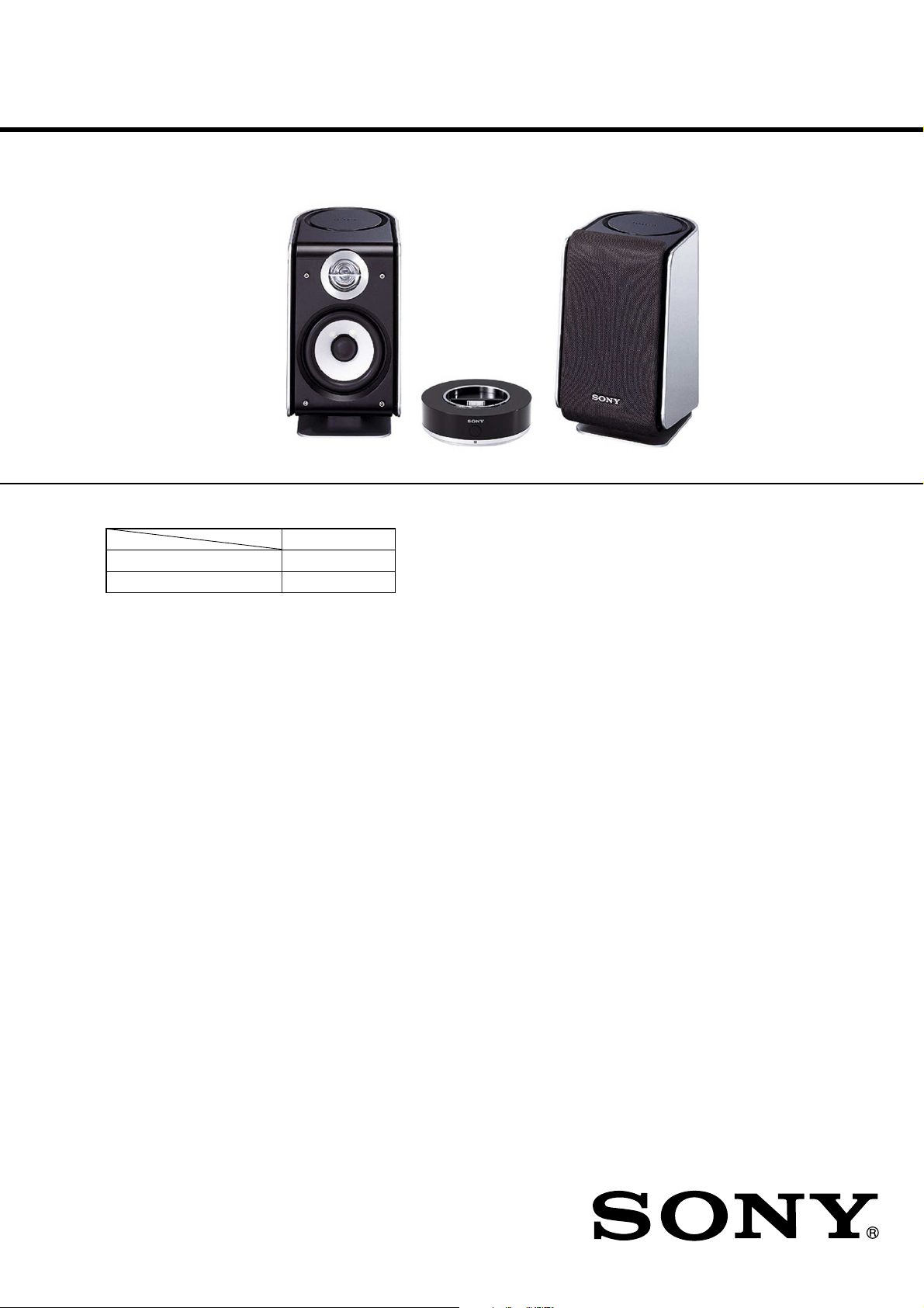
Photo: SRS-NWZ10C Photo: SRS-NWZ10SPhoto: SRS-NWZ10S
• This set is composed of the following models.
SRS-NWZ10
Cradle SRS-NWZ10C
Speaker SRS-NWZ10S
Note: SRS-NWZ10S is described in the accessories.
US Model
Canadian Model
AEP Model
UK Model
SPECIFICATIONS
Speaker section
Speaker system 2 way built-in passive radiator,
Impedance 3.2 Ω
Rated input power 4 W
Maximum input power 8 W
Amplifier section
Rated output 4 W + 4 W (10 % T.H.D., 1 kHz, 3.2 Ω)
Cradle section
Data input/output WM-PORT (22 pins) connector × 1,
Input Stereo minijack × 1
Input impedance WM-PORT (22 pins) 47 kΩ (at 1 kHz),
General
Power DC 12 V (supplied AC power adaptor)
Dimensions (w/h/d) Approx. 100 × 32 × 100 mm
Mass
Supplied accessories
AC power adaptor (1)
Mains lead (1)
Card Remote Commander (1)
Lithium battery CR2025 (1) (preinstalled for the trial use)
Operating Instructions (1)
Warranty (1) (AEP and UK models only)
Supported Walkman
WALKMAN to fulfill following requirement.
• WM-PORT (22 pins) compatible
• Supplied circular attachment
Design and specifications are subject to change without notice.
Magnetically shielded
80 mm (woofer), 25 mm (tweeter)
WM-PORT (22 pins) jack × 1
Stereo minijack 8 kΩ (at 1 kHz)
5
(4 × 1
/16 × 4 in.) (cradle)
Approx. 100 × 183 × 159 mm
1
/4 × 63/8 in.) (speaker)
(4 × 7
Approx. 100g (4 oz.) (cradle)
Approx. 950 g (2 lb. 2 oz.) (left speaker)
Approx. 930 g (2 lb. 1 oz.) (right speaker)
9-887-487-02
2007A05-1
© 2007.01
ACTIVE SPEAKER SYSTEM
Sony Corporation
Personal Audio Division
Published by Sony Techno Create Corporation
SRS-NWZ10
Ver. 1.1
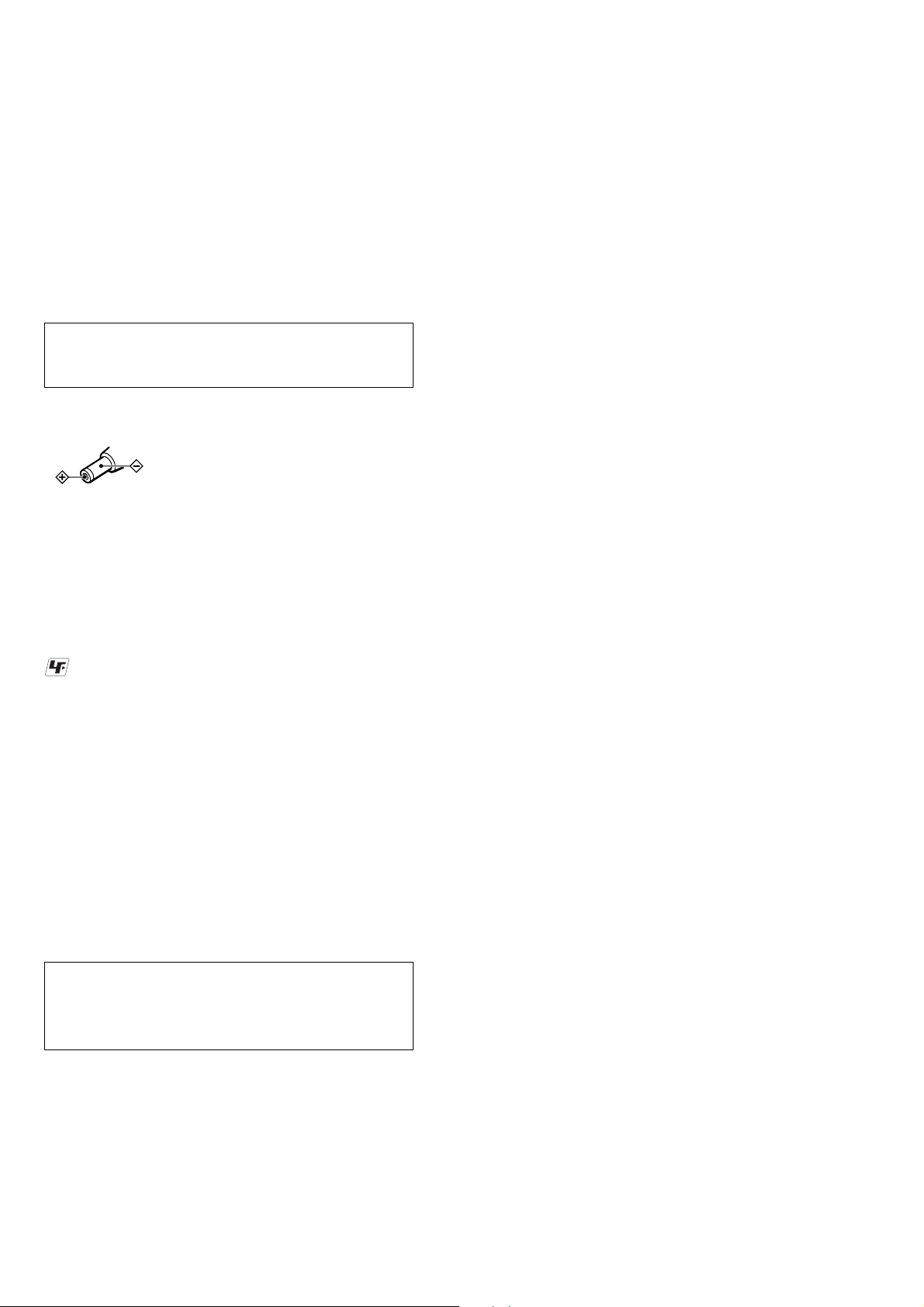
Notes on chip component replacement
• Never reuse a disconnected chip component.
• Notice that the minus side of a tantalum capacitor may be
damaged by heat.
Flexible Circuit Board Repairing
• Keep the temperature of the soldering iron around 270 ˚C
during repairing.
• Do not touch the soldering iron on the same conductor of the
circuit board (within 3 times).
• Be careful not to apply force on the conductor when soldering
or unsoldering.
WARNING
Danger of explosion if battery is incorrectly replaced.
Replace only with the same of equivalent type.
Notes on the AC power adaptor
• Use only the supplied AC power adaptor. Do not use any other
AC power adaptor to avoid damaging the speaker.
Polarity of the plug
• Before connecting or disconnecting the AC power adaptor, turn
off the system. Otherwise, it may cause a malfunction.
UNLEADED SOLDER
Boards requiring use of unleaded solder are printed with the leadfree mark (LF) indicating the solder contains no lead.
(Caution: Some printed circuit boards may not come printed with
the lead free mark due to their particular size)
: LEAD FREE MARK
Unleaded solder has the following characteristics.
• Unleaded solder melts at a temperature about 40 °C higher
than ordinary solder.
Ordinary soldering irons can be used but the iron tip has to be
applied to the solder joint for a slightly longer time.
Soldering irons using a temperature regulator should be set to
about 350 °C.
Caution: The printed pattern (copper foil) may peel away if
the heated tip is applied for too long, so be careful!
• Strong viscosity
Unleaded solder is more viscou-s (sticky, less prone to flow)
than ordinary solder so use caution not to let solder bridges
occur such as on IC pins, etc.
• Usable with ordinary solder
It is best to use only unleaded solder but unleaded solder may
also be added to ordinary solder.
Refer to SUPPLEMENT-1 for the MAIN board of printed wiring
boards, schematic diagrams and electrical parts list of US and
Canadian models. When repairing the set of AEP and UK models,
refer to either of original service manual/SUPPLEMENT-1
according to the set.
SAFETY-RELATED COMPONENT WARNING!!
COMPONENTS IDENTIFIED BY MARK 0 OR DOTTED LINE
WITH MARK 0 ON THE SCHEMATIC DIAGRAMS AND IN
THE PARTS LIST ARE CRITICAL TO SAFE OPERATION.
REPLACE THESE COMPONENTS WITH SONY PAR TS WHOSE
PART NUMBERS APPEAR AS SHOWN IN THIS MANU AL OR
IN SUPPLEMENTS PUBLISHED BY SONY.
2
ATTENTION AU COMPOSANT AYANT RAPPORT
À LA SÉCURITÉ!
LES COMPOSANTS IDENTIFIÉS P AR UNE MARQ UE 0 SUR
LES DIAGRAMMES SCHÉMATIQUES ET LA LISTE DES
PIÈCES SONT CRITIQUES POUR LA SÉCURITÉ DE
FONCTIONNEMENT. NE REMPLACER CES COM- POSANTS
QUE PAR DES PIÈCES SONY DONT LES NUMÉROS SONT
DONNÉS DANS CE MANUEL OU D ANS LES SUPPLÉMENTS
PUBLIÉS PAR SONY.
SECTION 1
B
A
M
U
T
I
N
G
V
O
L
V
O
L
M
U
T
I
N
G
V
O
L
V
O
L
Front
Avant
Rear
Arrière
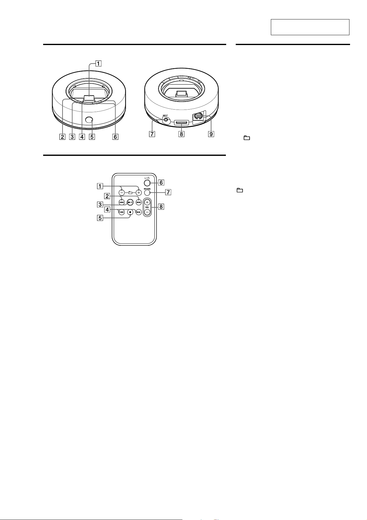
Identifying parts
Cradle
(See fig. A)
1 WM-PORT connector (for connecting to Walkman)
2 I/1 (power/standby) indicator
3 I/1 (power/standby) button
4 MUTING indicator
5 Remote sensor
6 VOL (volume) +/− buttons
7 INPUT (audio input) jack
8 WM-PORT jack (for connecting to a PC)
9 L OUT jack
Card remote commander
(See fig. B)
1 (folder) +/− buttons
2 .> (go to the beginning of the previous or next track)
buttons
3 N X (play/pause) button
4 m M (rewind/fast-forward) buttons
5 x (stop) button
6 I/1 (power/standby) button
7 MUTING (muting) button
8 VOL (volume) +/− buttons
(folder) +/− buttons find the beginning of the first track of
each group in the order selected on the Walkman.
Note
Some operations of the card remote commander may not work, or
work differently as indicated, depending on the specification of
the Walkman you are using.
WM-PORT
GENERAL
SRS-NWZ10
This section is extracted from
instruction manual.
3

SRS-NWZ10
SECTION 2
DIAGRAMS
• Note for Printed Wiring Boards and Schematic Diagrams
Note on Printed Wiring Board:
• X : parts extracted from the component side.
• Y : parts extracted from the conductor side.
• : Pattern from the side which enables seeing.
(The other layers' patterns are not indicated.)
Caution:
Pattern face side: Parts on the pattern face side seen from
(Conductor Side) the pattern face are indicated.
Parts face side: Parts on the parts face side seen from
(Component Side) the parts face are indicated.
Note on Schematic Diagram:
• All capacitors are in µF unless otherwise noted. (p: pF)
50 WV or less are not indicated except for electrolytics
and tantalums.
• All resistors are in Ω and 1/
specified.
• C : panel designation.
• A : B+ Line.
• Voltages and waveform are dc with respect to ground
under no-signal conditions.
no mark : POWER ON
• Voltages are taken with a VOM (Input impedance 10 MΩ).
Voltage variations may be noted due to normal production tolerances.
• Waveform are taken with a oscilloscope.
Voltage variations may be noted due to normal production tolerances.
• Circled numbers refer to waveform.
• Signal path.
F : AUDIO
N : USB
4
W or less unless otherwise
• Waveform
– MAIN Board –
IC901 2 (OUT)
1
9.65 µs
5 V/DIV, 5 µs/DIV
12.6 Vp-p
4
SRS-NWZ10
Ver. 1.1
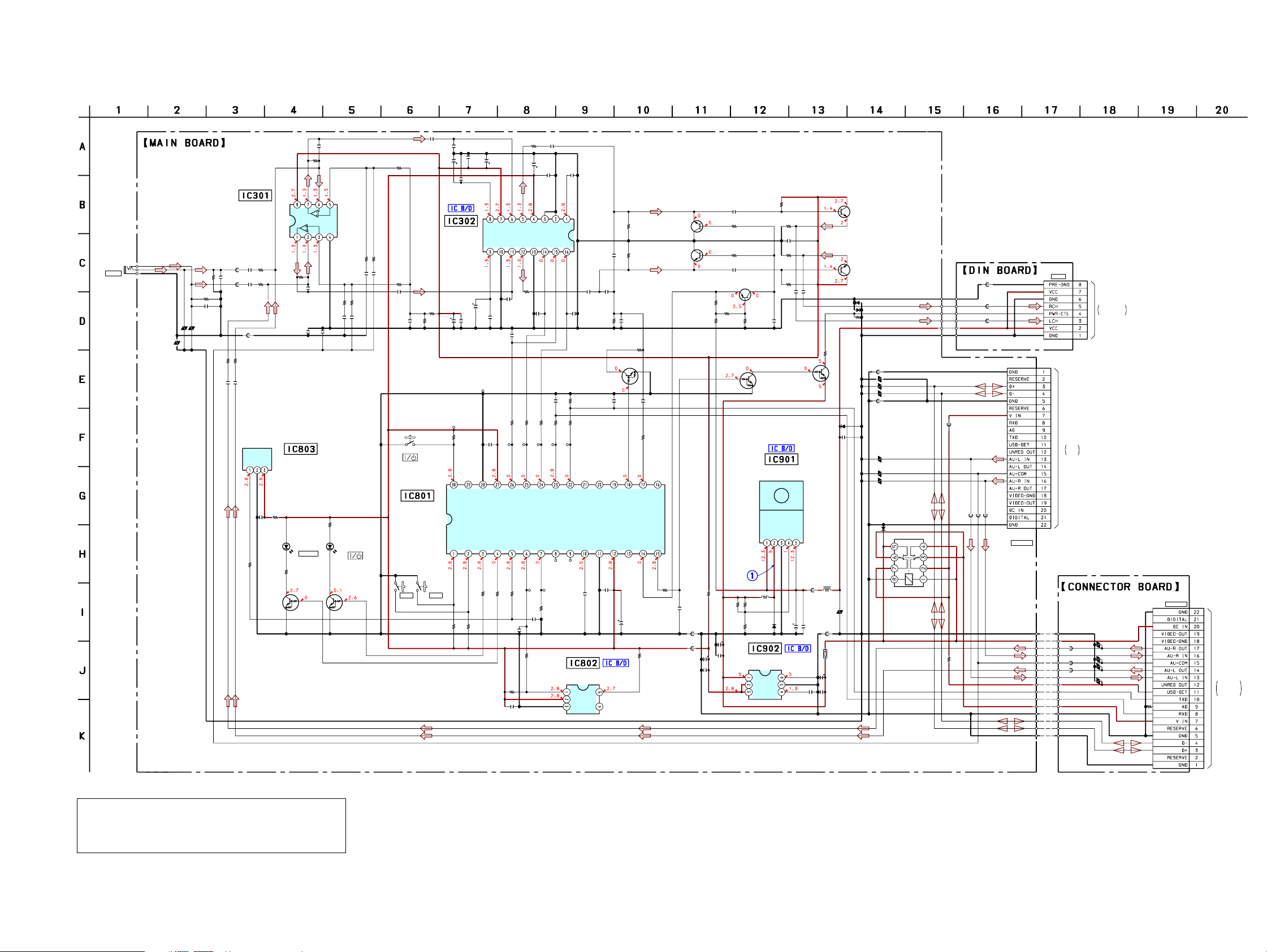
2-1. SCHEMATIC DIAGRAM
C101
J301
INPUT
1
0
1
R
D
V
VDR301
100p
R101
18k
R201
18k
1
C201
0
2
100p
R
D
V
R203
47k
C203
0.1
• See page 4 for Waveform. • See page 8 for IC Block Diagrams. • See page 8 for IC Pin Function Description.
R108 C112
1k 1
C309
100
6.3V
C307
0.022
2
T
D
D
IN
S
U
D
D
L
O
V
L
T
D
S
U
S
O
V
R
D
R208
1k
C311
100p
A
N
T
-E
A
O
-D
O
0
T
D
E
S
M
E
L
R
F
TP902TP901 C803
FLMD0#RST 0.1
R820
1k
R
D
N
A
E
L
M
C807 C808R814
100p 100p220k
R802
10k
V
A
S
S
IN
V
A
R
C210
100p
R809 R810 R811 R812 R813
470 470 470 100 100
TP905 TP904 TP903 TP908 TP909
SCK SI SO TX RX
F
K
E
C
R
-S
V
0
A
E
T
D
O
E
M
L
E
M
O
I-R
R819
47k
C812
0.1
C308
1000p
1
N
S
T
R
S
D
R
A
T
K
C
D
M
M
X
X
T
I-R
O
1
2
X
X
TP911TP910
X1X2
RESET SIGNAL GENERATOR
BU4223G
OUT
VDD
GNDCTNC
R109
22k
C111
R209
470p
22k
C212
1
C211
470p
C310C312
100p100p
1
D
R
O
C
I-
C
G
E
R
IC802
C313
R303 R305 R307
10k 1k 47k
1000p
Q803
DTC114YUA
BUFFER
C809
0.1
7
2
P
1
E
D
P
E
R
O
-B
IN
I-C
-M
O
D
0
S
6
D
S
V
V
P
C802
10
16V
Q101
2SC5996
MUTING
Q201
2SC5996
MUTING
R824
470
P
R
E
W
E
-P
-B
O
O
E
Y
T
B
U
T
S
-M
-
O
O
R801
470
C801
1000p
FB904
R825
470k
FB903
C910
100
10V
C909
1
R904
22
R304
10k
R110
100
R210
100
C213
1
Q301
2SA1576A
MUTING CONTROL SWITCH
R306
1M
R903 R902 L901
12k 12k
R901
1.5k
C906
220
10V
C907
1
BH28MA3WHFV-TR
FB101
NJM2740V-TE2
C102
C202
FB301
R103
47k
C103
0.1
R823
1k
LINE AMP
IC301
0.1
0.1
T
U
O
R
R102
56k
R202FB201
56k
D
N
G
C813
0.1
C
REMOTE CONTROL RECEIVER
C
V
JC801
0
R822
68
C104
33p
R104
47k
C
C
V
R204
47k
C204
33p
C301 C315
10 10
IC803
PRM7240-H5
R821
47
D802
SML-310LTT86
MUTING
Q802 Q801
DTC114YUA DTC114YUA
LED DRIVE LED DRIVE
D
N
G
R205 R206
56k 47k
C205
0.1
SML-310LTT86
R105 R106
56k 47k
C105
0.1
C206
0.047
D801
0.047
C106
R107
47k
R207
47k
C207
1
S803
SYSTEM CONTROLLER
IC801
µPD78F05D1MC (S)
-5A4-E2-A
S802 S801
VOL- VOL+
C110 C306
C107
100p 0.022
1
R302
2.2k
R301C303
2.2k10
C305C108
100
10
6.3V
16V
C109
0.022
L
ELECTRICAL
VOLUME
IC302
SM6451BT-G-E2
C304
220
6.3V
TP906
+VDD
R808
10k
3
Y
E
I-K
1
Y
E
I-K
R807 R806 C811 C805
10k 10k 1 100p
R
V
R
R
V
C208
10
16V
C209
C302
0.022
0.1
TP907
GND
C806 R817
0.1 1k
3
S
2
S
P
V
A
2
D
Y
E
E
L
-
I-K
O
R805 R804 R803 C804
1k 1k 1k 1
C314
0.01
DTC114YUA
100µH
D902
RB051L
-40TE25
+2.8V REGULATOR
IC902
IN
OUT
OUT
Q302,303
STANDBY SWITCH
Q303
DC/DC CONVERTER
IC901
BD9702CP-V5
T
U
O
IN
STBY
GND
NOISE
R111C113
100k1
R112
1k
C316
1
R212
1k
R211
100k
C114 C214
11
Q302
DTA114YUA
Y
D
B
V
N
T
G
IN
S
C903
220
25V
Q102
2SC4081T106R
BUFFER
Q202
2SC4081T106R
BUFFER
D302
1SS355-TE17
1SS355-TE17
D301
47k
R308 FB102
R309
1k
FB401
VDR401
VDR403
VDR402
FB402
D901
RB051L-40TE25
C901
0.1
VDR406
VDR405
VDR404
D401
1SS355-TE17
-2 -1
L902
22µH
FB901
VDR901
C902
FB902
0.1
TH401
C904
220
10V
C905
0.1
C908
0.01
66
11
RY401
J901
8P
15 15
L OUT
FOR
SRS-NWZ10S
FOR
PC
CN402
22P
WM-PORT
FB409
VDR410
VDR409
FB408
VDR408
FB407
VDR407
R402
22k
NETWORK
WALKMAN
FOR
FB302
FB202
FB403
4
5
6
0
0
0
4
4
4
B
B
B
F
F
F
CN401
22P
WM-PORT
R401
0
Refer to SUPPLEMENT-1 for the MAIN board of schematic
diagrams of US and Canadian models. When repairing the set of
AEP and UK models, refer to either of original service manual/
SUPPLEMENT-1 according to the set.
SRS-NWZ10
11
55

SRS-NWZ10
Ver. 1.1
• Semiconductor
Location
Ref. No. Location
D401 C-6
D801 E-5
D802 F-5
D902 D-4
IC301 D-8
Q302 D-5
Q303 D-5
Q801 F-5
Q802 F-6
2-2. PRINTED WIRING BOARDS – MAIN Section (1/2) –
1 2 3 4 5 6 7 8
A
CONNECTOR BOARD
(COMPONENT SIDE)
R402
B
115
11
1-872-591-
(11, 12)
C
D
: Uses unleaded solder.
CONNECTOR BOARD
FOR
NETWORK WALKMAN
25811141720
1471013161922
36912151821
FB409
VDR408
FB407
FB408
VDR409
VDR410
MAIN BOARD
L902
L901
(CONDUCTOR SIDE)
CN402
WM-PORT
VDR407
1-872-591-
(COMPONENT SIDE)
D902
R308
R309
11
(11, 12)
Q302
Q303
CN401
WM-PORT
15
TH401
FB406
(FOR PC)
FB405
D401
FB404
FB403
RY401
–2
–1
FB402
FB401
1
C301
C102
C307
C306
C107
C104
R105
R102
R104
R107
R302
C105
R301
R205
C303
C205
IC301
C202
R202
R204
R207
C204
C207
Refer to SUPPLEMENT-1 for the
MAIN board of printed wiring
boards of US and Canadian
models. When repairing the set
of AEP and UK models, refer to
either of original service manual/
SUPPLEMENT-1 according to
the set.
SRS-NWZ10
E
G
C804
C803
A
R821
D801
K
1
D801, 802
A
F
K
Q801
R808
D802
MUTING
A
R822
K
Q802
C811
C806
1-872-590-
R807
R806
11
(11)
66
 Loading...