

Page 1
SRF-T615
SERVICE MANUAL
Ver 1.0 1999.10
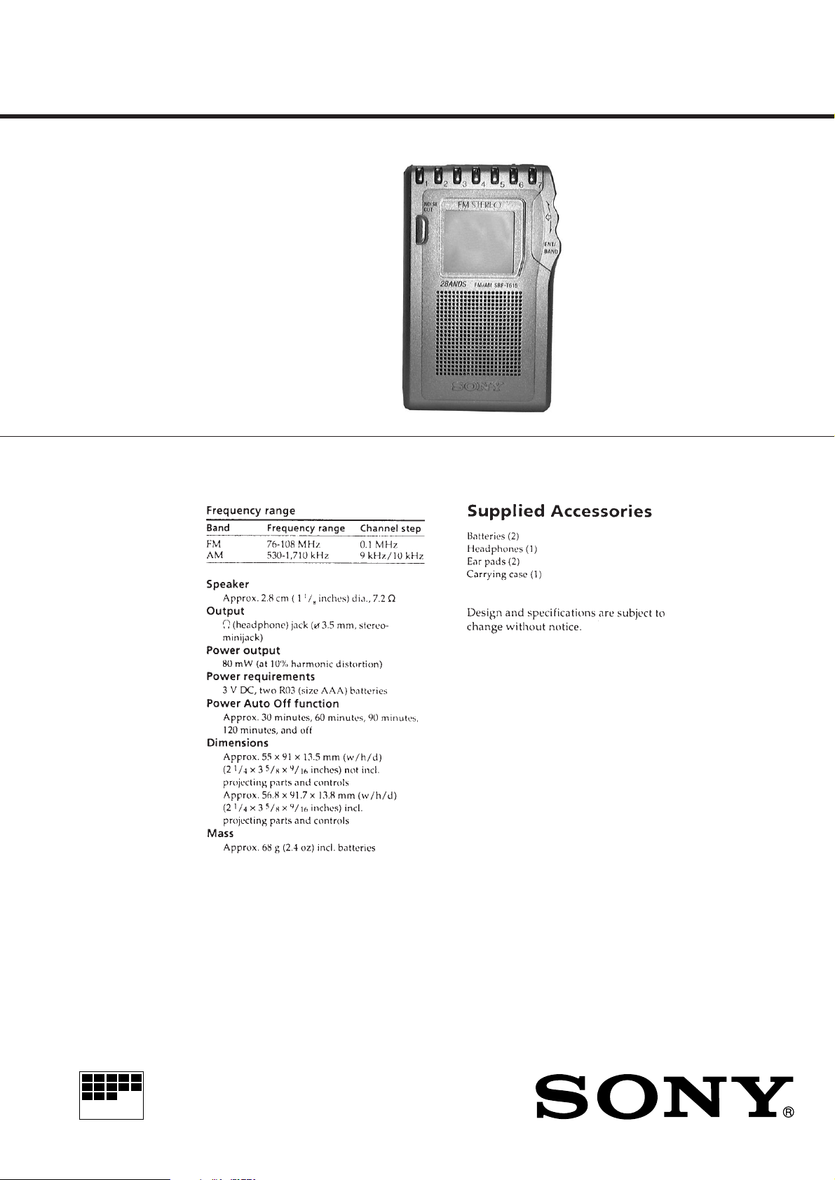
SPECIFICATIONS
Tourist Model
MICROFILM
FM STEREO/AM PLL SYNTHESIZED RADIO
Page 2
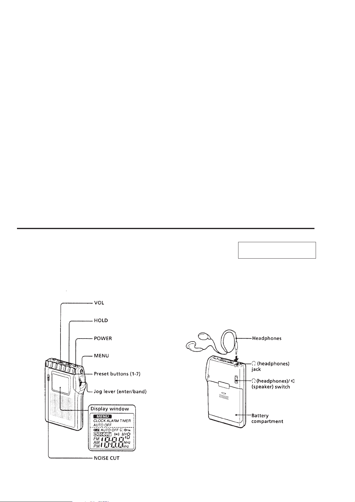
TABLE OF CONTENTS
Specifications ........................................................................... 1
1. GENERAL
Location and Function of Controls .................................... 2
2. DISASSEMBLY
2-1. Cover (JOG) (A) ......................................................... 3
2-2. Lid, Battery Case ........................................................ 3
2-3. Cabinet (Rear)............................................................. 4
2-4. Main Board ................................................................. 4
3. ADJUSTMENTS .......................................................... 5
4. DIAGRAMS
4-1. Explanation of IC Terminals....................................... 7
4-2. Block Diagrams .......................................................... 9
4-3. Printed Wiring Boards .............................................. 12
4-4. Schematic Diagram................................................... 15
5. EXPLODED VIEW..................................................... 19
6. ELECTRICAL PARTS LIST.................................... 20
Flexible Circuit Board Repairing
• Keep the temperature of the soldering iron around 270°C during
repairing.
• Do not touch the soldering iron on the same conductor of the
circuit board (within 3 times).
• Be careful not to apply force on the conductor when soldering or
unsoldering.
Notes on chip component replacement
• Never reuse a disconnected chip component.
• Notice that the minus side of a tantalum capacitor may be damaged by heat.
LOCATION AND FUNCTION OF CONTROLS
SECTION 1
GENERAL
This section is extracted from
instruction manual.
– 2 –
Page 3
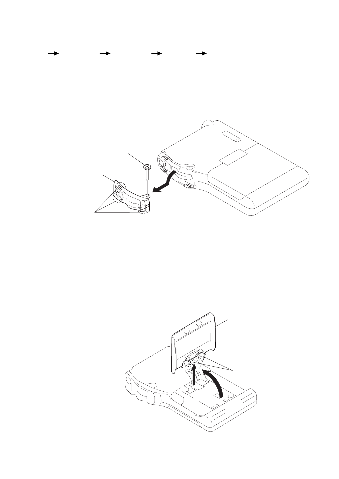
DISASSEMBLY
e
r
The equipment can be removed using the following procedure.
SECTION 2
Set
Cover (JOG) (A)
Lid, Battery Case Cabinet (Rear) Main Board
Note : Follow the disassembly procedure in the numerical order given.
2-1. COVER (JOG) (A)
1
Screw (B1.7x9)
Cover (JOG) (A)
3
Turn from upper side
of the cover (JOG) (A),
2
Three claws
and remove it.
2-2. LID, BATTERY CASE
Lid, battery cas
3
Two claws
2
1
– 3 –
Page 4
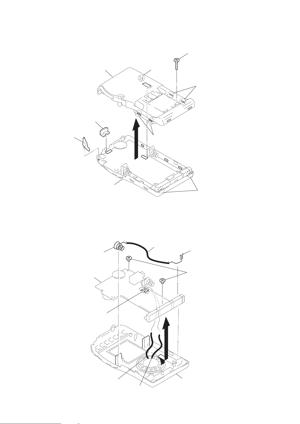
2-3. CABINET (REAR)
s
y
1
Screw (1.7x9)
5
Button (MENU)
Cabinet (rear)
4
Knod (HOLD)
Cabinet (front) ASSY
3
2
Claw
2
Two claws
2
Two claws
2
Two claw
2-4. MAIN BOARD
Terminal (–) (A), battery
Main board
3
Remove solder
1
Lead wire (Black)
4
Terminal (+) (A), batter
2
Screws (1.4)
Brown
Cabinet (front) ASSY
Black
– 4 –
Page 5
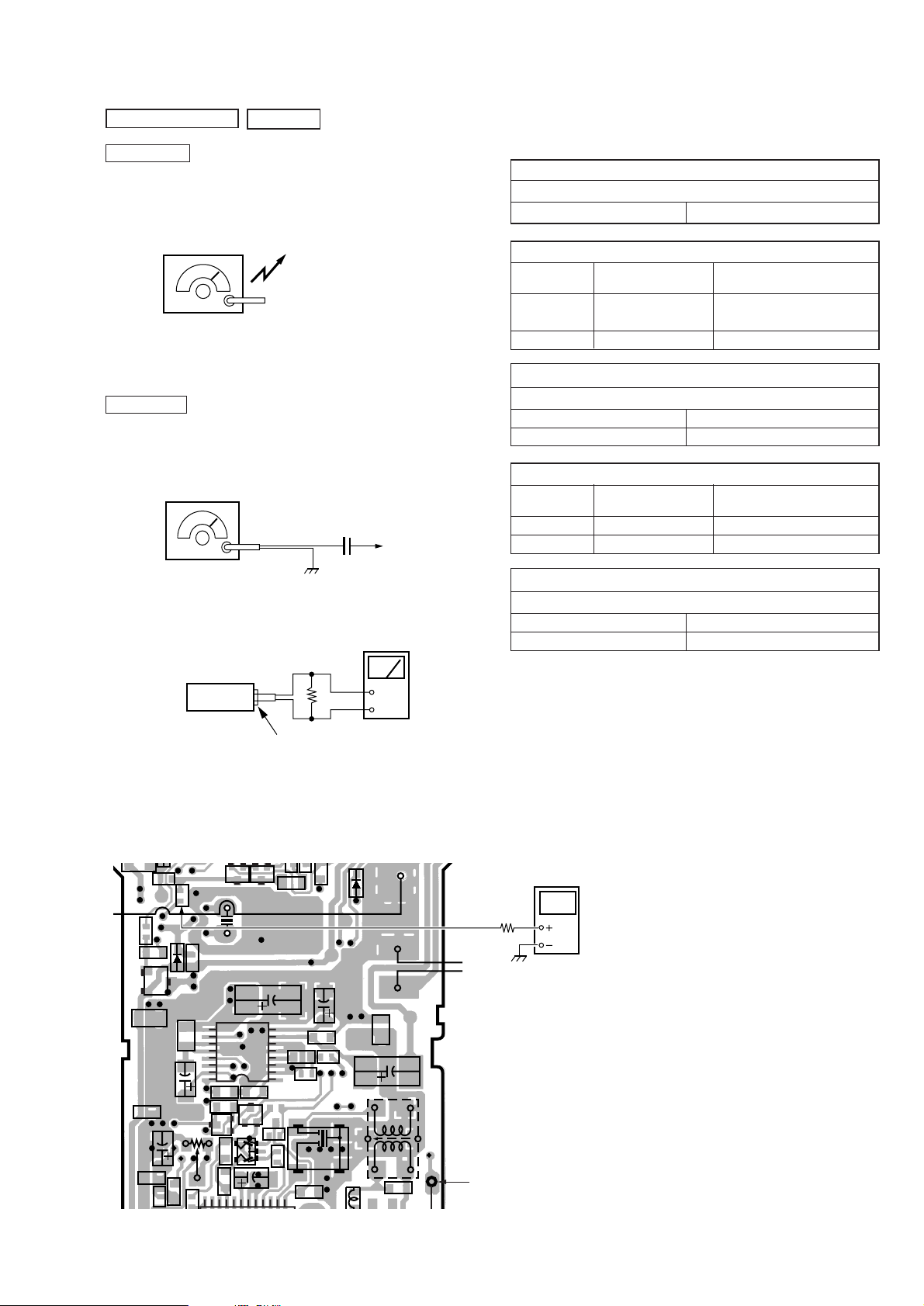
SECTION 3
)
r
D
C603
5
5
r
ADJUSTMENTS
TUNER SECTION
AM Section
Band : AM
Volume : MIN
AM RF signal
generator
30% amplitude modulation by 400Hz
signal.
Output level : as low as possible
FM Section
Band : FM
Volume : MIN
FM RF signal
generator
0dB = 1µ V
Put the lead-wire
antenna close to
the set.
0.01
µ
F
TP102 (RF IN
MAIN board
• Repeat the procedures in each adjustment several times, and the
frequency coverage and tracking adjustments should be finally
done by the trimmer capacitors.
AM IF ADJUSTMENT
Adjust for a maximum reading on level meter.
T101 450kHz
AM FREQUENCY COVERAGE ADJUSTMENT
Adjust part Frequency display
L103 531kHz
Confirmation 1,710kHz 7.8 – 10.8V
AM TRACKING ADJUSTMENT
Adjust for a maximum reading on level meter.
L104 585kHz
CT101 1,485kHz
FM FREQUENCY COVERAGE CONFIRMATION
Adjust part Frequency display
Confirmation 76.0MHz 2.2 – 4.2V
Confirmation 108.0MHz 7.5 – 10.5V
reading on digital
voltmeter.
Adjustment Value : 2.5V
Standard Value : 2.45 – 2.55V
reading on digital
voltmeter.
22.5kHz frequency deviation by
400Hz signal.
Output level : as low as possible
set
Frequency Coverage Adjustment
Connect Location :
[MAIN BOARD] (SIDE B)
R533
D501
C314
RV201
R542
12
16
Q202
116
Q504
X501
C312
C201
ECB
IC301
BCE
C131
C127
R541
R603
C608
Q602
C605
R607
C207
BE
C206
C
C301
R201
C204
16
Ω
Headphone jack (J301)
R
Q201
R119
Q103
C121
C504
89
5
C307
1
R120
13152024
R
C308
R310
R309
CF102
C124
ECB
Q503
C311
C313
BCE
-1
C51
level mete
C310
106
+
–
D104
C17
C309
T101
C120
R533
100k
TP102
(RF IN)
FM TRACKING ADJUSTMENT
Adjust for a maximum reading on level meter.
L101 76.0MHz
CT102 108.0MHz
Digital
voltmete
Ω
– 5 –
Page 6

FM VCO Adjustment
)
t
R203
4
C302
r
Procedure :
FM RF signal
generator
0.01
µ
F
TP102 (RF IN
MAIN board
Carrier frequency : 98MHz
Modulation : no modulation
Output level : 100dB
µ
V (100mV)
1. Connect the frequency counter to 3 to 4 pins of IC201 as shown
the figure.
2. Turn the set to 98MHz.
3. Adjust RV201 for 76.0kHz reading on frequency counter.
Standard Value : 75.95 –76.05kHz
Connect Location :
[MAIN BOARD] (SIDE A)
C209
R20
C133
117
C105
C102
R104
ECB
D102
C130
R126
Q104
R114
C125
R102
BCE
C126
R124
R123
C109
C113
C104
D103
-1
-3
C103
10
1
R202
C129
R112
-2
C208
IC201
CF101
R107
C110
R103
C205
Q102
R111
R110
ECB
C132
C111
D101
R109
C107
6
5
R105
R108
IC201
IC201
3
1-674-988-
4
33k
frequency counte
1µF
Ω
Adjustment Location :
[MAIN BOARD] (SIDE B)
RV201 : FM VCO Adjustment
IC101
T101 : AM IF Adjustment
L103 : AM Frequency Coverage
Adjustment
CT101 : AM Tracking Adjustment
L101 : FM Tracking Adjustmen
L104 : AM Tracking Adjustment
CT102 : FM Tracking Adjustment
– 6 –
Page 7

SECTION 4
DIAGRAMS
4-1. EXPLANATION OF IC TERMINALS
IC502 µPD17073GB-925-9EU (SYSTEM CONTROL, LCD DRIVE)
Pin No. Pin name I/O Description
1 DO — Not used (OPEN).
2 EEPROM CS — Not used (OPEN).
3 TV 4-12CH — Not used (OPEN).
4 MUTE O Audio mute signal output.
5 NC — Not used (Connect to ground).
6 POWER O Power ON/OFF control output.
7 KS0 O Key source signal output. *1
8 KS1 O Key source signal output. *1
9 KS2 O Key source signal output. *1
10 KS3 O Key source signal output. *1
11 KR0 I Key return signal input.
12 NC — Not used (Connect to ground).
13 KR1 I Key return signal input. *1
14 KR2 I Key return signal input. *1
15 KR3 I Key return signal input. *1
16 METER O Meter drive signal output (Not used : OPEN).
17 ST/MONO O Stereo/ Mono control signal output.
18 V DET2 I Voltage decrease detection input. “L” : less than 2.1V (Change to clock mode).
19 BAND O Band select output. “H” : AM, “L” : FM
20 GND — Ground terminal.
21 GND — Ground terminal.
22 EO O PLL error signal output for PLL LPF.
23 VCOL I VCO input.
24 VCOH — Not used (OPEN).
25 REG0 — Capacitor connection terminal for LCD drive voltage.
26 VDD — Power supply terminal (3V).
27 VDD — Power supply terminal (3V).
28 X OUT O System clock output (75kHz).
29 X IN I System clock input (75kHz).
30 REG1 — Capacitor connection terminal for LCD drive voltage.
31 LEG LCD0 — Capacitor connection terminal for LCD drive voltage.
32 CAP LCD0 — Capacitor connection terminal for LCD drive voltage.
33 CAP2 LCD1 — Capacitor connection terminal for LCD drive voltage.
34 LEG LCD1 — Capacitor connection terminal for LCD drive voltage.
35 COM0 O Common signal output for LCD.
36 COM1 O Common signal output for LCD.
37 COM2 O Common signal output for LCD.
38 NC — Not used (Connect to ground).
39 COM3 O Common signal output for LCD.
40 LCD0 O Segment signal output for LCD.
41 LCD1 O Segment signal output for LCD.
42 LCD2 O Segment signal output for LCD.
43 LCD3 O Segment signal output for LCD.
44 LCD4 O Segment signal output for LCD.
45 NC — Not used (Connect to ground).
– 7 –
Page 8

Pin No. Pin name I/O Description
46 LCD5 O Segment signal output for LCD.
47 LCD6 O Segment signal output for LCD.
48 LCD7 O Segment signal output for LCD.
49 LCD8 O Segment signal output for LCD.
50 LCD9 O Segment signal output for LCD.
51 LCD10 O Segment signal output for LCD.
52 LCD11 O Segment signal output for LCD.
53 LCD12 O Segment signal output for LCD.
54 NC — Not used (Connected to ground).
55 LCD13 O Segment signal output for LCD.
56 LCD14 O Segment signal output for LCD.
57 CE I Voltage decrease detection input. “L” : less than 1.9V (Change to clock mode).
58 INT I Hold switch input terminal. “L” : Hold
59 NC — Not used (Connect to ground).
60 BEEP O Beep signal output.
61 NOISE CUT O Noise filter circuit control signal output.
62 — Not used (OPEN)
63 — Not used (Fixed at “L”)
64 DI — Not used.
*1 Key matrix
KR0 (qa pin)
KR1 (qd pin)
KR2 (qf pin)
KR3 (qg pin)
KS0 (7 pin) KS1 (8 pin) KS2 (9 pin) KS3 (q; pin)
Preset station <1> POWER ENT/BAND Preset station <5>
S502 S503 S504 (JOG) S505
Preset station <4> NOISE CUT TUNE <->
S506 S507 S504 (JOG)
Preset station <2> Preset station <6>
S508 S509
Preset station <3> MENU TUNE <+> Preset station <7>
S510 S511 S504 (JOG) S512
– 8 –
Page 9

4-2. BLOCK DIAGRAMS
SRF-T615
– 9 – – 11 –– 10 –
• Signal path.
F : FM
Page 10

SRF-T615
4-3. PRINTED WIRING BOARDS
C606
T601
R605
2
R602
(LITHIUM BATTERY)
C601
R601
C602
C603
C608
Q602
C605
R607
C206
C207
C122
AM FERRITE-ROD
ANTENNA
S501
HOLD>
T
ON
BAT501
D602
D601
R541
R603
BE
C
D501
C301
C204
R201
R115
C114
L103
L104
OFF
R533
C314
RV201
1
r
Semiconductor
Location
Ref. No. Location
D101 G-9
D102 G-8
D103 G-9
D104 D-4
D301 C-5
D501 D-2
D601 C-2
D602 C-2
IC101 F-3
IC201 E-9
IC301 E-3
IC501 C-7
IC502 C-8
IC503 D-7
Q102 G-9
Q103 E-3
Q104 E-8
Q105 E-8
Q201 E-3
Q202 E-3
Q301 E-9
Q503 D-3
Q504 D-3
Q601 C-4
Q602 D-2
Q603 C-1
Q604 C-1
Note:
• X : parts extracted from the component side.
r
•
• b : Pattern from the side which enables seeing.
(The other layers' patterns are not indicated.)
Caution:
Pattern face side: Parts on the pattern face side seen from the
(Side B) pattern face are indicated.
Parts face side: Parts on the parts face side seen from the
(Side A) parts face are indicated.
: Through hole.
– 12 – – 14 –– 13 –
A
[MAIN BOARD] (SIDE B)
S503
POWER
B
C
D
E
F
G
H
02
S511
MENU
R604
C607
C604
BCE
Q604
ECB
R606
Q603
BAT601
DRY BATTERY
SIZE "AAA"
(IEC DESIGNATION R03)
2PCS, 3V
ECB
Q504
X501
R542
12
IC301
16
C312
C201
Q202
BCE
C131
C127
R116
C128
IC101
15
L102
CT101 CT102
3 4 5 6 7
J301
i
[MAIN BOARD] (SIDE A)
C521
C313
BCE
C116
L105
R506
C506
R522
ECB
Q503
C311
Q201
R119
-1
10 12
R125
R510
C507
C504
89
5
1
Q103
C121
13152024
C115
C112
RV301
C523
C508
R520
R521
R531
C307
R309
R120
R113
C124
CF103
VOL
R504
C510
R509
R517
ECB
Q601
C519
R536
C511
C308
R310
CF102
L101
1-674-988-
C310
L106
R516
D104
C309
R505
C503
C17
T101
C120
R308
L302
R305
R508
R307
R301
S301 S302
R304
C315
TP102
(RF IN)
11
(11)
L303
D301
SP401
SPEAKER
C306
S301,302
S502
1
R306
C305
i
5
S507
NOISE
CUT
S508
L301
8
2
TP511
(VT)
S510
3
14 578910
R502 R503
2 1
3 4
C518
1
5
10
15
16
R534
2
1
C502
R535
R539
IC501
C509
R518
R523
R526
R528
R529
3
4
IC503
C501
C524
64
17
C525
60
IC502
20 25
C512
R538
R540
S506
4
R511
55
LCD501
50
R537
R530
L501
Q105
C117
30
C513
C304
C302
C133
C105
C102C106
R104
49
32
C514
R303
ECB
D102
C505
C516
R302
C130
S505
48
45
40
35
33
R126
R114
C125
R102
5
C517C515
C303
R203
BCE
Q104
C126
D103
-1
-3
C103
15 19
R311
BCE
Q301
R204
R124
10
IC201
R123
1
R202
CF101
C129
R112
C109
C113
C104
-2
R103
9 10
S512
7
(–)
(+)
1-674-988-
C202
C203
C209
C208
C205
R107
C110
D101
S509
6
R532
Q102
R111
R110
ECB
R105
C132
C111
R109
C107
(BAND)
6
5
R108
11
(11)
ı
S504
ENTER/
BAND
Page 11

4-4. SCHEMATIC DIAGRAM
r
Refer to page 18 for IC Block Diagrams.
r
WA VEFORMS
1
SRF-T615
1.7 Vp-p
75 kHz
IC502 wk
X OUT
2
466 nsec
T601
3
343 nsec
Q603 BASE
4
VOLT/DIV : 0.5 V AC
TIME/DIV : 5 µsec
13.2 Vp-p
VOLT/DIV : 2 V AC
TIME/DIV : 0.2 µsec
230 mVp-p
VOLT/DIV : 50 mV AC
TIME/DIV : 0.1 µsec
3.5 Vp-p
319 nsec
Q603 COLLECTOR
VOLT/DIV : 1 V AC
TIME/DIV : 0.1 µsec
Note:
• All capacitors are in µF unless otherwise noted. pF: µµF
50 WV or less are not indicated except for electrolytics
and tantalums.
• All resistors are in Ω and 1/
specified.
• U : B+ Line.
• H : adjustment for repair.
• Power voltage is dc 3V and fed with regulated dc power
supply from battery terminal.
• Voltages and waveforms are dc with respect to ground
under no-signal (detuned) conditions.
no mark : FM
< > : AM
• Voltages are taken with a V OM (Input impedance 10 MΩ).
Voltage variations may be noted due to normal production tolerances.
• Waveforms are taken with a oscilloscope.
Voltage variations may be noted due to normal production tolerances.
• Circled numbers refer to waveforms.
• Signal path.
F : FM
4
W or less unless otherwise
– 15 – – 17 –– 16 –
Page 12

SECTION 5
)
EXPLODED VIEW
MAIN
SECTION 6
ELECTRICAL PARTS LIST
r
IC BLOCK DIAGRAMS
IC101 CXA1111N IC201 LA3335M
R OUT
DET
FILTER
VCC
DETUNE
DET COUNT
24 23 22 21 20 19 18 17 16 15 14 13
BAND SIGNAL
OUTPUT CIRCUIT
FM.IF
DISCRI
AM.FE
FM.FE
1 2 3 4 5 6 7 8 9 10 11 12
GND
FM DISCRI
AFC
AM OSC
AFC/AGC 2
AFC/AGC 1
REG
FM OSC
RIPPLE
FILTER
IF GND
AM IF OUT
TUNING
METER
FM RF
AM RF IN
METER
NC
FM IF IN
FM RF IN
AM IF IN
AM.IF
DET.AGC
FE GND
BAND SELECT
REGULATOR
FM/AM
FE OUT
DECODER
STEREO
SWITCH
1
IN
IC301 CXA1522N
IN1
REG
15 14 13 12 11 10 9
16
REG VOL
1
2
3
NC
IN2
VOL
NC
NF1
GND1
P-GND1
PRE+POWER1
PRE+POWER2
5678
4
NF2
GND2
P-GND2
OUT1
OUT2
VCC
RIPPLE
L OUT
910
PHASE
COMPALATE
234
PLL
PLT DET
8
SYNC
DET
FF 1/2FF 90º
V.C.O VCO STOP
VCC
LAMP
TRIGGER
FF 0º
VCO
GND
IND
6
7
5
NC
NOTE :
• -XX, -X mean standardized parts, so they
may have some difference from the original
one.
• Items marked “ * ”are not stocked since they
are seldom required for routine service. Some
• The mechanical parts with no reference
number in the exploded views are not
supplied.
• Accessories and packing materials are given
in the last of this parts list.
delay should be anticipated when ordering
these items.
11
10
13
not
supplied
21
9
SP401
7
11
8
12
16
(4A)
14
not supplied
LCD501
15
not
supplied
21
19
17
14
(
4
B
6
22
3
4
2
not supplied
20
14
(4C)
5
L104
3
21
14
1
Ref. No. Part No. Description Remark Ref. No. Part No. Description Remark
1 3-039-058-01 LID,BATTERY CASE
2 3-318-203-91 SCREW(B1.7X9), TAPPING
3 3-309-597-41 SCREW(1.4), TAPPING
4 3-039-073-01 TERMINAL (+) (B), BATTERY
* 5 A-3683-119-A MAIN BOARD, COMPLETE
6 3-039-061-01 HOLDER (ANT)
7 3-039-074-01 TERMINAL (-) (B), BATTERY
8 3-039-072-01 TERMINAL (-) (A), BATTERY
9 3-039-071-01 TERMINAL (+) (A), BATTERY
10 X-3377-972-1 CABINET (FRONT) ASSY
11 3-035-166-01 SPACER (LCD)
12 3-039-068-11 COVER (JOG) (A)
13 3-039-069-01 BUTTON (PRESET)
14 3-039-081-01 COMBINED (KNOB)
(INCLUDING vA:KNOB (HOLD), vB:BUTTON,
(MENU), vC:KNOB (EAR/SP),
vD:HINGE(LID,BATTERY CASE))
15 1-694-596-11 CONDUCTIVE BOARD, CONNECTION
16 3-039-060-01 HOLDER (LCD)
17 3-039-059-01 BUTTON (POWER)
18 3-039-057-11 CABINET (REAR)
19 3-039-063-01 PLATE
20 3-042-771-01 SPACER (EP/SP)
21 3-831-441-99 CUSHION
* 22 3-036-658-01 SHEET, ADHESIVE
L104 1-501-974-21 ANTENNA, FERRITE-ROD (MW)
LCD501 1-803-791-11 DISPLAY PANEL, LIQUID CRYSTAL
SP401 1-529-187-11 SPEAKER (2.8cm)
18
2
(4D)
21
(AM TRACKING)
NOTE :
• Due to standardization, replacements in the
parts list may be different from the parts
specified in the diagrams or the components
used on the set.
• -XX, -X mean standardized parts, so they
may have some difference from the original
one.
• RESISTORS
All resistors are in ohms
• SEMICONDUCTORS
In each case, u : µ , for example :
uA.... : µ A.... , uPA.... : µPA....
uPB.... : µ PB.... , uPC.... : µ PC....
uPD.... : µ PD....
• CAPACITORS
uF : µ F
• COILS
uH : µ H
When indicating parts by reference number, please include the board.
METAL : Metal-film resistor
METAL OXIDE :Metal oxide-film resistor
F : nonflammable
• Items marked “ * ”are not stocked since
they are seldom required for routine service.
Some delay should be anticipated when
ordering these items.
Ref. No. Part No. Description Remark Ref. No. Part No. Description Remark
* A-3683-119-A MAIN BOARD, COMPLETE
C202 1-164-156-11 CERAMIC CHIP 0.1uF 25V
*********************
C203 1-164-156-11 CERAMIC CHIP 0.1uF 25V
1-694-596-11 CONDUCTIVE BOARD, CONNECTION
* 3-036-658-01 SHEET, ADHESIVE
3-039-060-01 HOLDER (LCD)
3-039-061-01 HOLDER (ANT)
C204 1-164-156-11 CERAMIC CHIP 0.1uF 25V
C205 1-115-416-11 CERAMIC CHIP 1000PF 5% 25V
C206 1-135-201-11 TANTALUM CHIP 10uF 20% 4V
C207 1-162-970-11 CERAMIC CHIP 0.01uF 10% 25V
3-831-441-99 CUSHION, STOPPER
C208 1-164-245-11 CERAMIC CHIP 0.015uF 10% 25V
* 4-920-257-01 COVER, INSULATING, FLEXIBLE
C209 1-164-245-11 CERAMIC CHIP 0.015uF 10% 25V
C301 1-119-663-11 TANTAL. CHIP 47uF 20% 2.5V
< BATTERY >
C302 1-125-837-91 CERAMIC CHIP 1uF 10% 6.3V
C303 1-164-156-11 CERAMIC CHIP 0.1uF 25V
BAT501 1-528-412-11 BATTERY, PAS SECONDARY
C304 1-125-837-91 CERAMIC CHIP 1uF 10% 6.3V
< CAPACITOR >
C305 1-127-569-91 TANTAL. CHIP 100uF 20% 4V
C306 1-162-927-11 CERAMIC CHIP 100PF 5% 50V
C102 1-162-970-11 CERAMIC CHIP 0.01uF 10% 25V
C103 1-162-970-11 CERAMIC CHIP 0.01uF 10% 25V
C307 1-125-837-91 CERAMIC CHIP 1uF 10% 6.3V
C308 1-125-837-91 CERAMIC CHIP 1uF 10% 6.3V
C104 1-164-357-11 CERAMIC CHIP 1000PF 5% 50V
C105 1-162-910-11 CERAMIC CHIP 5PF 0.25PF 50V
C106 1-164-357-11 CERAMIC CHIP 1000PF 5% 50V
C309 1-125-899-11 TANTAL. CHIP 220uF 20% 4V
C310 1-135-201-11 TANTALUM CHIP 10uF 20% 4V
C311 1-125-899-11 TANTAL. CHIP 220uF 20% 4V
C107 1-162-921-11 CERAMIC CHIP 33PF 5% 50V
C109 1-162-907-11 CERAMIC CHIP 2PF 0.25PF 50V
C312 1-162-964-11 CERAMIC CHIP 0.001uF 10% 50V
C313 1-162-964-11 CERAMIC CHIP 0.001uF 10% 50V
C110 1-165-325-11 CERAMIC CHIP 680PF 2% 50V
C111 1-109-864-91 CERAMIC CHIP 68PF 2% 50V
C112 1-162-919-11 CERAMIC CHIP 22PF 5% 50V
C314 1-109-982-11 CERAMIC CHIP 1uF 10% 10V
C315 1-107-826-91 CERAMIC CHIP 0.1uF 10% 16V
C501 1-115-156-11 CERAMIC CHIP 1uF 10V
C113 1-162-907-11 CERAMIC CHIP 2PF 0.25PF 50V
C114 1-162-964-11 CERAMIC CHIP 0.001uF 10% 50V
C502 1-164-156-11 CERAMIC CHIP 0.1uF 25V
C503 1-164-156-11 CERAMIC CHIP 0.1uF 25V
C115 1-162-927-11 CERAMIC CHIP 100PF 5% 50V
C116 1-163-021-91 CERAMIC CHIP 0.01uF 10% 50V
C117 1-135-201-11 TANTALUM CHIP 10uF 20% 4V
C504 1-110-501-11 CERAMIC CHIP 0.33uF 10% 16V
C505 1-162-974-11 CERAMIC CHIP 0.01uF 50V
C506 1-162-966-11 CERAMIC CHIP 0.0022uF 10% 50V
C120 1-164-315-11 CERAMIC CHIP 470PF 5% 50V
C121 1-135-201-11 TANTALUM CHIP 10uF 20% 4V
C507 1-162-966-11 CERAMIC CHIP 0.0022uF 10% 50V
C508 1-162-966-11 CERAMIC CHIP 0.0022uF 10% 50V
C122 1-127-569-91 TANTAL. CHIP 100uF 20% 4V
C124 1-162-970-11 CERAMIC CHIP 0.01uF 10% 25V
C125 1-115-156-11 CERAMIC CHIP 1uF 10V
C509 1-162-966-11 CERAMIC CHIP 0.0022uF 10% 50V
C510 1-162-970-11 CERAMIC CHIP 0.01uF 10% 25V
C511 1-164-156-11 CERAMIC CHIP 0.1uF 25V
C126 1-164-505-11 CERAMIC CHIP 2.2uF 16V
C127 1-165-176-11 CERAMIC CHIP 0.047uF 10% 16V
C512 1-164-346-11 CERAMIC CHIP 1uF 16V
C513 1-162-921-11 CERAMIC CHIP 33PF 5% 50V
C128 1-115-156-11 CERAMIC CHIP 1uF 10V
C129 1-115-156-11 CERAMIC CHIP 1uF 10V
C130 1-164-245-11 CERAMIC CHIP 0.015uF 10% 25V
C514 1-162-918-11 CERAMIC CHIP 18PF 5% 50V
C515 1-164-156-11 CERAMIC CHIP 0.1uF 25V
C516 1-164-156-11 CERAMIC CHIP 0.1uF 25V
C131 1-164-363-11 CERAMIC CHIP 560PF 5% 50V
C132 1-162-917-11 CERAMIC CHIP 15PF 5% 50V
C517 1-164-156-11 CERAMIC CHIP 0.1uF 25V
C518 1-164-156-11 CERAMIC CHIP 0.1uF 25V
C133 1-115-156-11 CERAMIC CHIP 1uF 10V
C201 1-115-156-11 CERAMIC CHIP 1uF 10V
C519 1-162-957-11 CERAMIC CHIP 220PF 5% 50V
– 18 – – 20 –– 19 –
Page 13

MAIN
Ref. No. Part No. Description Remark Ref. No. Part No. Description Remark
C521 1-162-970-11 CERAMIC CHIP 0.01uF 10% 25V
C523 1-162-970-11 CERAMIC CHIP 0.01uF 10% 25V
C524 1-162-970-11 CERAMIC CHIP 0.01uF 10% 25V
C525 1-162-970-11 CERAMIC CHIP 0.01uF 10% 25V
C601 1-164-850-11 CERAMIC CHIP 10PF 0.5PF 16V
C602 1-164-156-11 CERAMIC CHIP 0.1uF 25V
C603 1-164-346-11 CERAMIC CHIP 1uF 16V
C604 1-162-915-11 CERAMIC CHIP 10PF 0.5PF 50V
C605 1-164-346-11 CERAMIC CHIP 1uF 16V
C606 1-135-201-11 TANTALUM CHIP 10uF 20% 4V
C607 1-164-156-11 CERAMIC CHIP 0.1uF 25V
C608 1-115-156-11 CERAMIC CHIP 1uF 10V
< FILTER >
CF101 1-781-419-71 FILTER, CERAMIC(DISCRIMINATOR)
CF102 1-767-480-11 FILTER, CERAMIC (AM)
CF103 1-577-588-81 FILTER, CERAMIC
< TRIMMER >
CT101 1-141-615-21 CAP, ADJ (AM TRACKING)
CT102 1-141-615-21 CAP, ADJ (FM TRACKING)
< DIODE >
D101 8-719-023-99 DIODE KV1563M-3
D102 8-713-102-96 DIODE 1T403-M20-T8A
D103 8-713-102-96 DIODE 1T403-M20-T8A
D104 8-719-046-91 DIODE MA2S111
D301 8-719-800-76 DIODE 1SS226
D501 8-719-071-34 DIODE RB521S-30-TE61
D601 8-719-046-91 DIODE MA2S111
D602 8-719-420-87 DIODE MA8130
< IC >
IC101 8-752-065-30 IC CXA1111N
IC201 8-759-804-98 IC LA3335M
IC301 8-752-065-32 IC CXA1522N
IC501 8-759-578-28 IC S-80819ANNP-EDG-T2
IC502 8-759-643-72 IC uPD17073GB-925-9EU
IC503 8-759-568-85 IC S-80821ANNP-EDJ-T2
LCD501 1-803-791-11 DISPLAY PANEL, LIQUID CRYSTAL
Q102 8-729-037-89 TRANSISTOR 2SC4627J-C(TX).SO
Q103 8-729-429-44 TRANSISTOR XP1501
Q104 8-729-037-92 TRANSISTOR 2SD2216J-R(TX).SO
Q105 8-729-037-71 TRANSISTOR UN9210J-(TX).SO
Q201 8-729-037-74 TRANSISTOR UN9213J-(TX).SO
Q202 8-729-037-61 TRANSISTOR UN9113J-(TX).SO
Q301 8-729-037-53 TRANSISTOR 2SB1462J-QR(TX).SO
Q503 8-729-037-92 TRANSISTOR 2SD2216J-R(TX).SO
Q504 8-729-037-92 TRANSISTOR 2SD2216J-R(TX).SO
Q601 8-729-037-71 TRANSISTOR UN9210J-(TX).SO
Q602 8-729-800-71 TRANSISTOR 2SB815B7-TB
Q603 8-729-037-92 TRANSISTOR 2SD2216J-R(TX).SO
Q604 8-729-037-92 TRANSISTOR 2SD2216J-R(TX).SO
R102 1-218-990-11 SHORT 0
R103 1-218-965-11 RES,CHIP 10K 5% 1/16W
R104 1-218-977-11 RES,CHIP 100K 5% 1/16W
R105 1-218-977-11 RES,CHIP 100K 5% 1/16W
R107 1-218-969-11 RES,CHIP 22K 5% 1/16W
R108 1-218-989-11 RES,CHIP 1M 5% 1/16W
R109 1-218-989-11 RES,CHIP 1M 5% 1/16W
R110 1-218-969-11 RES,CHIP 22K 5% 1/16W
R111 1-218-945-11 RES,CHIP 220 5% 1/16W
R112 1-218-945-11 RES,CHIP 220 5% 1/16W
R113 1-218-945-11 RES,CHIP 220 5% 1/16W
R114 1-218-965-11 RES,CHIP 10K 5% 1/16W
R115 1-218-929-11 RES,CHIP 10 5% 1/16W
R116 1-218-965-11 RES,CHIP 10K 5% 1/16W
R119 1-218-977-11 RES,CHIP 100K 5% 1/16W
R120 1-218-973-11 RES,CHIP 47K 5% 1/16W
R123 1-218-977-11 RES,CHIP 100K 5% 1/16W
R124 1-218-965-11 RES,CHIP 10K 5% 1/16W
R125 1-218-953-11 RES,CHIP 1K 5% 1/16W
R126 1-218-971-11 RES,CHIP 33K 5% 1/16W
< LIQUID CRYSTAL DISPLAY >
< TRANSISTOR >
< RESISTOR >
< JACK >
J301 1-793-513-21 JACK (i)
< COIL >
L101 1-416-903-41 COIL (WITH CORE) (FM TRACKING)
L102 1-414-693-11 INDUCTOR 150nH
L103 1-406-493-41 COIL (AM OSC) (AM FREQUENCY COVERAGE)
L104 1-501-974-21 ANTENNA, FERRITE-ROD (MW)
(AM TRACKING)
L105 1-412-977-11 INDUCTOR 0.68uH
L106 1-412-995-21 INDUCTOR 22uH
L301 1-412-987-31 INDUCTOR 4.7uH
L302 1-412-987-31 INDUCTOR 4.7uH
L303 1-412-987-31 INDUCTOR 4.7uH
L501 1-412-995-21 INDUCTOR 22uH
R201 1-218-937-11 RES,CHIP 47 5% 1/16W
R202 1-218-970-11 RES,CHIP 27K 5% 1/16W
R203 1-218-965-11 RES,CHIP 10K 5% 1/16W
R204 1-218-965-11 RES,CHIP 10K 5% 1/16W
R301 1-218-959-11 RES,CHIP 3.3K 5% 1/16W
R302 1-218-937-11 RES,CHIP 47 5% 1/16W
R303 1-218-973-11 RES,CHIP 47K 5% 1/16W
R304 1-218-977-11 RES,CHIP 100K 5% 1/16W
R305 1-218-990-11 SHORT 0
R306 1-218-941-11 RES,CHIP 100 5% 1/16W
R307 1-218-953-11 RES,CHIP 1K 5% 1/16W
R308 1-218-941-11 RES,CHIP 100 5% 1/16W
R309 1-218-937-11 RES,CHIP 47 5% 1/16W
R310 1-218-973-11 RES,CHIP 47K 5% 1/16W
R311 1-218-990-11 SHORT 0
R502 1-218-965-11 RES,CHIP 10K 5% 1/16W
R503 1-218-989-11 RES,CHIP 1M 5% 1/16W
R504 1-218-965-11 RES,CHIP 10K 5% 1/16W
– 21 –
Page 14

SRF-T615
MAIN
Ref. No. Part No. Description Remark Ref. No. Part No. Description Remark
R505 1-218-965-11 RES,CHIP 10K 5% 1/16W
R506 1-218-989-11 RES,CHIP 1M 5% 1/16W
R508 1-218-965-11 RES,CHIP 10K 5% 1/16W
R509 1-218-953-11 RES,CHIP 1K 5% 1/16W
R510 1-218-965-11 RES,CHIP 10K 5% 1/16W
R511 1-218-965-11 RES,CHIP 10K 5% 1/16W
R516 1-218-973-11 RES,CHIP 47K 5% 1/16W
T101 1-416-019-11 TRANSFORMER, IF (AM) (AM IF)
T601 1-435-090-21 TRANSFORMER, DC-DC CONVERTER
X501 1-767-718-31 VIBRATOR, CRYSTAL (75kHz)
< TRANSFORMER >
< VIBRATOR >
R517 1-218-977-11 RES,CHIP 100K 5% 1/16W
R518 1-218-953-11 RES,CHIP 1K 5% 1/16W
R520 1-218-953-11 RES,CHIP 1K 5% 1/16W
R521 1-218-953-11 RES,CHIP 1K 5% 1/16W
R522 1-218-953-11 RES,CHIP 1K 5% 1/16W
R523 1-218-953-11 RES,CHIP 1K 5% 1/16W
R526 1-218-953-11 RES,CHIP 1K 5% 1/16W
R528 1-218-953-11 RES,CHIP 1K 5% 1/16W
R529 1-218-953-11 RES,CHIP 1K 5% 1/16W
R530 1-218-929-11 RES,CHIP 10 5% 1/16W
R531 1-218-965-11 RES,CHIP 10K 5% 1/16W
R532 1-218-990-11 SHORT 0
R533 1-218-965-11 RES,CHIP 10K 5% 1/16W
R534 1-218-989-11 RES,CHIP 1M 5% 1/16W
R535 1-218-965-11 RES,CHIP 10K 5% 1/16W
R536 1-218-965-11 RES,CHIP 10K 5% 1/16W
R537 1-218-961-11 RES,CHIP 4.7K 5% 1/16W
R538 1-218-965-11 RES,CHIP 10K 5% 1/16W
R539 1-218-965-11 RES,CHIP 10K 5% 1/16W
R540 1-218-965-11 RES,CHIP 10K 5% 1/16W
R541 1-218-977-11 RES,CHIP 100K 5% 1/16W
R542 1-218-989-11 RES,CHIP 1M 5% 1/16W
R601 1-218-953-11 RES,CHIP 1K 5% 1/16W
R602 1-218-937-11 RES,CHIP 47 5% 1/16W
R603 1-218-957-11 RES,CHIP 2.2K 5% 1/16W
**************************************************************
MISCELLANEOUS
*************
15 1-694-596-11 CONDUCTIVE BOARD, CONNECTION
L104 1-501-974-21 ANTENNA, FERRITE-ROD (MW)
(AM TRACKING)
LCD501 1-803-791-11 DISPLAY PANEL, LIQUID CRYSTAL
SP401 1-529-187-12 SPEAKER (2.8cm)
**************************************************************
ACCESSORIES & PACKING MATERIALS
*******************************
3-867-371-11 MANUAL, INSTRUCTION (JAPANESE,
CHINESE)
3-867-371-21 MANUAL, INSTRUCTION (ENGLISH, KOREAN)
8-953-301-93 RECEIVER,EAR MDR-E805LP
X-3329-657-1 ATTACHMENT
R604 1-218-981-11 RES,CHIP 220K 5% 1/16W
R605 1-218-977-11 RES,CHIP 100K 5% 1/16W
R606 1-218-973-11 RES,CHIP 47K 5% 1/16W
R607 1-218-989-11 RES,CHIP 1M 5% 1/16W
< VARIABLE RESISTOR >
RV201 1-223-586-11 RES, ADJ, CARBON 10K (FM VCO)
RV301 1-225-886-11 RES, VAR, CARBON 20K/20K (VOL )
< SWITCH >
S301 1-771-790-21 SWITCH, SLIDE (5 t i)
S302 1-771-390-11 SWITCH, SLIDE (5 t i)
S501 1-771-790-21 SWITCH, SLIDE (HOLD >)
S502 1-771-138-21 SWITCH, KEY BOARD (1)
S503 1-692-088-11 SWITCH, TACTILE (POWER)
S504 1-771-568-21 SWITCH, LEVER SLIDE (JOG)(ENT/BAND)
S505 1-771-138-21 SWITCH, KEY BOARD (5)
S506 1-771-138-21 SWITCH, KEY BOARD (4)
S507 1-771-138-21 SWITCH, KEY BOARD (NOISE CUT)
S508 1-771-138-21 SWITCH, KEY BOARD (2)
S509 1-771-138-21 SWITCH, KEY BOARD (6)
S510 1-771-138-21 SWITCH, KEY BOARD (3)
S511 1-692-088-11 SWITCH, TACTILE (MENU)
S512 1-771-138-21 SWITCH, KEY BOARD (7)
9-927-184-11
Sony Corporation
Personal Audio Company
– 22 –
Printed in Japan © 1999.10
99J02031-1
Published by General Engineering Dept.
 Loading...