

Page 1
SERVICE MANUAL
SPECIFICATIONS
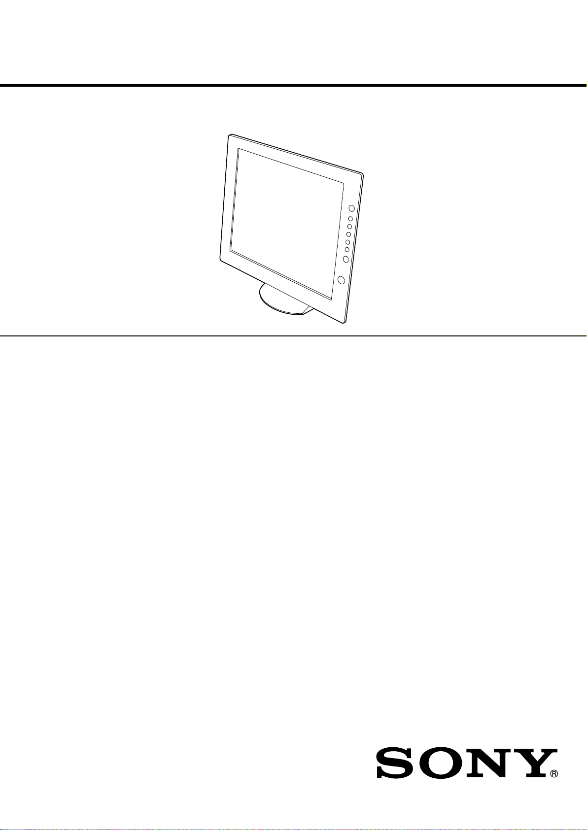
SDM-X72
US Model
Canadian Model
AEP Model
Chinese Model
LCD panel Panel type: a-Si TFT Active Matrix
Picture size: 17.0 inch
Input signal format RGB operating frequency*
Horizontal: 28 – 92 kHz
Vertical: 56 – 85 Hz
Resolution Horizontal: Max.1280 dots
Vertical: Max.1024 lines
Input signal levels Analog RGB video signal
0.7 Vp-p, 75 Ω , positive
SYNC signal
TTL level, 2.2 kΩ ,
positive or negative
(Separate horizontal and vertical,
or composite sync)
0.3 Vp-p, 75Ω , negative
(Sync on green)
Digital RGB (DVI) signal: TMDS
(Single link)
Power requireme n ts 100 – 240 V, 50 – 60 Hz,
0.9
Max. A
Power consumption
Operating temperature 5 – 35
Max. 40 W
°
C
Dimensions (width/height/depth)
Display (upright):
Approx. 438 ×410 × 227 mm
1
/4 × 16 1/4 × 9 inches)
(17
(with stand)
Approx. 438 × 356 × 84 mm
1
/4 × 14 1/8 ×3 3/8inches)
(17
(without stand)
Mass
Plug & Play DDC2B
* Recommended horizon tal and vertical timing condition
• Horizontal sync width dut y should be more than 4. 8% of total
horizontal time or 0.8 µs, whichever is larger.
• Horizontal blanking width should be more than 2.5 µsec.
• Vertical blanking width sh ould be more than 450 µsec.
Design and specification s are subject to change without noti ce.
Approx. 7.1 kg (15 lb 10 oz) (with
stand)
Approx. 5.3 kg (11 lb 11 oz)
(without stand)
TFT LCD Color Computer Display
Page 2
1.5 k
Ω
0.15 µF
AC
Voltmeter
(0.75 V)
To Exposed Metal
Parts on Set
Earth Ground
SAFETY CHECK-OUT
After correcting the original service problem, perform the following safety
checks before releasing the set to the customer:
1. Check the area of your repair for unsoldered or poorly-soldered
connections. Check the entire board surface for solder splashes and
bridges.
2. Check the interboard wiring to ensure that no wires are “pinched” or
contact high-wattage resistors.
3. Check that all control knobs, shields, covers, ground straps, and
mounting hardware have been replaced. Be absolutely certain that you
have replaced all the insulators.
4. Look for unauthorized replacement parts, particularly transistors, that
were installed during a previous repair. Point them out to the customer
and recommend their replacement.
5. Look for parts which, though functioning, show obvious signs of
deterioration. Point them out to the customer and recommend their
replacement.
6. Check the line cords for cracks and abrasion. Recommend the
replacement of any such line cord to the customer.
7. Check the connector shell, metal trim, “metallized” knobs, screws, and
all other exposed metal parts for AC Leakage. Check leakage as described right.
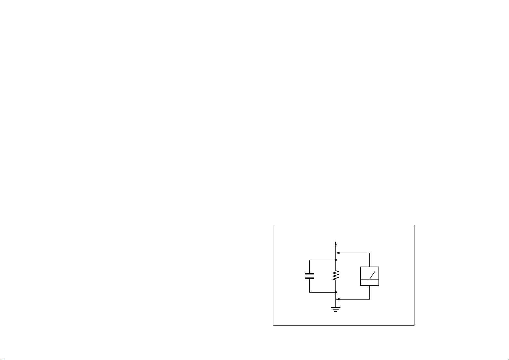
LEAKAGE TEST
The AC leakage from any exposed metal part to earth ground and from all
exposed metal parts to any exposed metal part having a return to chassis,
must not exceed 0.5 mA (500 microamperes).
Leakage current can be measured by any one of three methods.
1. A commercial leakage tester, such as the Simpson 229 or RCA WT540A. Follow the manufacturers’ instructions to use these instruments.
2. A battery-operated AC milliammeter. The Data Precision 245 digital
multimeter is suitable for this job.
3. Measuring the voltage drop across a resistor by means of a VOM or
battery-operated AC voltmeter. The “limit” indication is 0.75 V, so
analog meters must have an accurate low-voltage scale. The Simpson 250
and Sanwa SH-63Trd are examples of a passive VOMs that are suitable.
Nearly all battery operated digital multimeters that have a 2 V AC range
are suitable. (See Fig. A)
Fig. A. Using an AC voltmeter to check AC leakage.
SDM-X72(E) 2
Page 3

WARNING!!
AVERTISSEMENT!!
SAFETY-RELATED COMPONENT WARNING!!
COMPONENTS IDENTIFIED BY SHADING AND MARK ! ON THE
SCHEMATIC DIAGRAMS, EXPLODED VIEWS AND IN THE
PARTS LIST ARE CRITICAL FOR SAFE OPERATION. REPLACE
THESE COMPONENTS WITH SONY PARTS WHOSE PART
NUMBERS APPEAR AS SHOWN IN THIS MANUAL OR IN
SUPPLEMENTS PUBLISHED BY SONY. CIRCUIT ADJUSTMENTS THAT ARE CRITICAL FOR SAFE OPERATION ARE
IDENTIFIED IN THIS MANUAL. FOLLOW THESE PROCEDURES
WHENEVER CRITICAL COMPONENTS ARE REPLACED OR IMPROPER OPERATION IS SUSPECTED.
ATTENTION AUX COMPOSANTS RELATIFS À LA SÉCURITÉ!!
LES COMPOSANTS IDENTIFIÉS PAR UNE TRAME ET UNE
MARQUE ! SONT CRITIQUES POUR LA SÉCURITÉ. NE LES
REMPLACER QUE PAR UNE PIÈCE PORTANT LE NUMÉRO
SPECIFIÉ. LES RÉGLAGES DE CIRCUIT DONT L’IMPORTANCE EST
CRITIQUE POUR LA SÉCURITÉ DU FONCTIONNEMENT SONT
IDENTIFIÉS DANS LE PRÉSENT MANUEL. SUIVRE CES
PROCÉDURES LORS DE CHAQUE REMPLACEMENT DE
COMPOSANTS CRITIQUES, OU LORSQU’UN MAUVAIS
FONCTIONNEMENT EST SUSPECTÉ.
SDM-X72(E) 3
Page 4

POWER SAVING FUNCTION
g
AUTOMATIC PICTURE QUALITY ADJUSTMENT
FUNCTION
(ANALOG RGB)
This monitor meets the power-saving guidelines set by VESA,
E
NERGY STAR, and NUTEK. If the monitor is connected to a
computer or video graphics board that is DPMS (Display Power
Management Signaling) compliant, the monitor will
automatically reduce power consumption as shown below.
Power mode Power consumption
1
(power)
indicator
normal
40 W (max.) green
operation
active off*
3 W (max.) orange
(deep sleep)**
1 (power) off 1 W red
main power of f 0 W off
* When your computer enters the “active off” mode, the input signal is
cut and NO INPUT SI GNAL appears on the screen . After 10 s econds,
the monitor enters the po w er sa vin g m ode .
** “Deep sleep” is a powe r saving mode defined by t he Environmental
Protection Agency.
Note
ZZ...
If the (POWER SAVE) is set to OFF (page 16), th e monitor does not
enter the power saving mode.
When the monitor receives an input signal, it
automatically adjusts the picture’s position and
sharpness (phase/pitch), and ensures that a clear
picture appears on the screen.
The factory preset mode
When the monitor receives an input signal, it automatically
matches the signal to one of the fact ory preset modes stored in th e
monitor’s memory to provide a high quality picture at the center
of the screen. If the input signal matches the factory pre set mode,
the picture is appears on the screen automatically with the
appropriate default adjustment.
If input signals do not match one of the factory
preset modes
When the monitor receives an input signal , the automat ic pict ure
quality adjustment function of this monitor is activated and
ensures that a clear picture always appears on the screen (wit hin
the following monitor frequency ranges):
Horizontal frequency:
Vertical frequency:
Consequently, the first time the monitor receives input signals
that do not match one of the factory preset modes, the monitor
may take a longer time than normal for displaying the picture on
the screen. This adjustment data is automatically stored in
memory so that next time, the monitor will function in the same
way as when the monitor receives the signals that match one of
the factory preset modes.
28 – 92 kHz
56 – 85 Hz
If you adjust the phase, pitch, and pictures
position manually
For some input signals, the automatic picture quality adjustment
function of this monitor may not completely adjust the picture
position, phase, and pitch. In this case, yo u can manually set these
adjustments (page 13). If you manually set these adjustments,
they are stored in memory as user modes and automatically
recalled whenever the monitor receives the same input si
nals.
SDM-X72(E) 4
Page 5

TABLE OF CONTENTS
Section Title Page Section Title Page
1. DISASSEMBLY
1-1. Rear Cover and Cabinet Assy Removal ............... 1-1
1-2. H Board Removal ................................................ 1-2
1-3. I Board Removal .................................................. 1-3
1-4. A Board Removal ................................................ 1-4
1-5. G Board Removal ................................................ 1-5
1-6. U Board and LCD Unitl Removal......................... 1-6
1-7. LCD Panel Removal ............................................ 1-7
2. ADJUSTMENTS
2-1. Service Functions of Buttons in Front Panel ........ 2-1
2-2. Usea of Service Mode .......................................... 2-2
2-3. Functions of Service Mode .................................. 2-3
3. DIAGRAMS
3-1. Block Diagrams .................................................... 3-1
3-2. Circuit Boards Location........................................ 3-2
3-3. Schematic Diagrams and Printed Wiring Boards.. 3-3
(1)Schematic Diagram
of A(a,b,c,d,e,f,g,h) Board......... 3-4
(2)Schematic Diagram of H Board. ...................... 3-13
(3)Schematic Diagram of I Board......................... 3-15
(4)Schematic Diagram of U Board. ...................... 3-17
(5)Schematic Diagram of G Board. ...................... 3-19
4. EXPLODED VIEWS
4-1. Chassis ................................................................. 4-2
2-4. White Balance Adjustment .................................. 2-3
2-5. Action after Replacing
the LCD Panel and Board ..................................... 2-5
4-2. Packing Materials ................................................. 4-3
5. ELECTRICAL PARTS LIST ............................... 5-1
SDM-X72(E) 5
Page 6
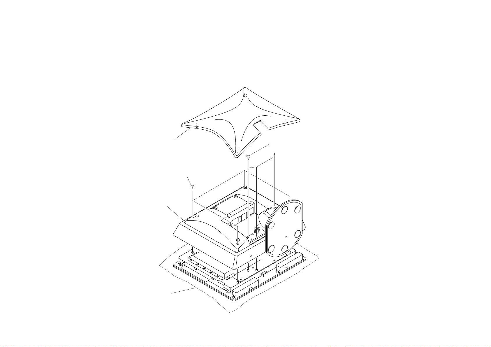
1-1. REAR COVER AND CABINET ASSY REMOVAL
SECTION 1
DISASSEMBLY
1 Rear cover
3 Four screws
(+PWH 3X12)
4 Cabinet assy
Protection sheet
2 Four screws
(+PSW 4X10)
SDM-X72(E) 1-1
Page 7
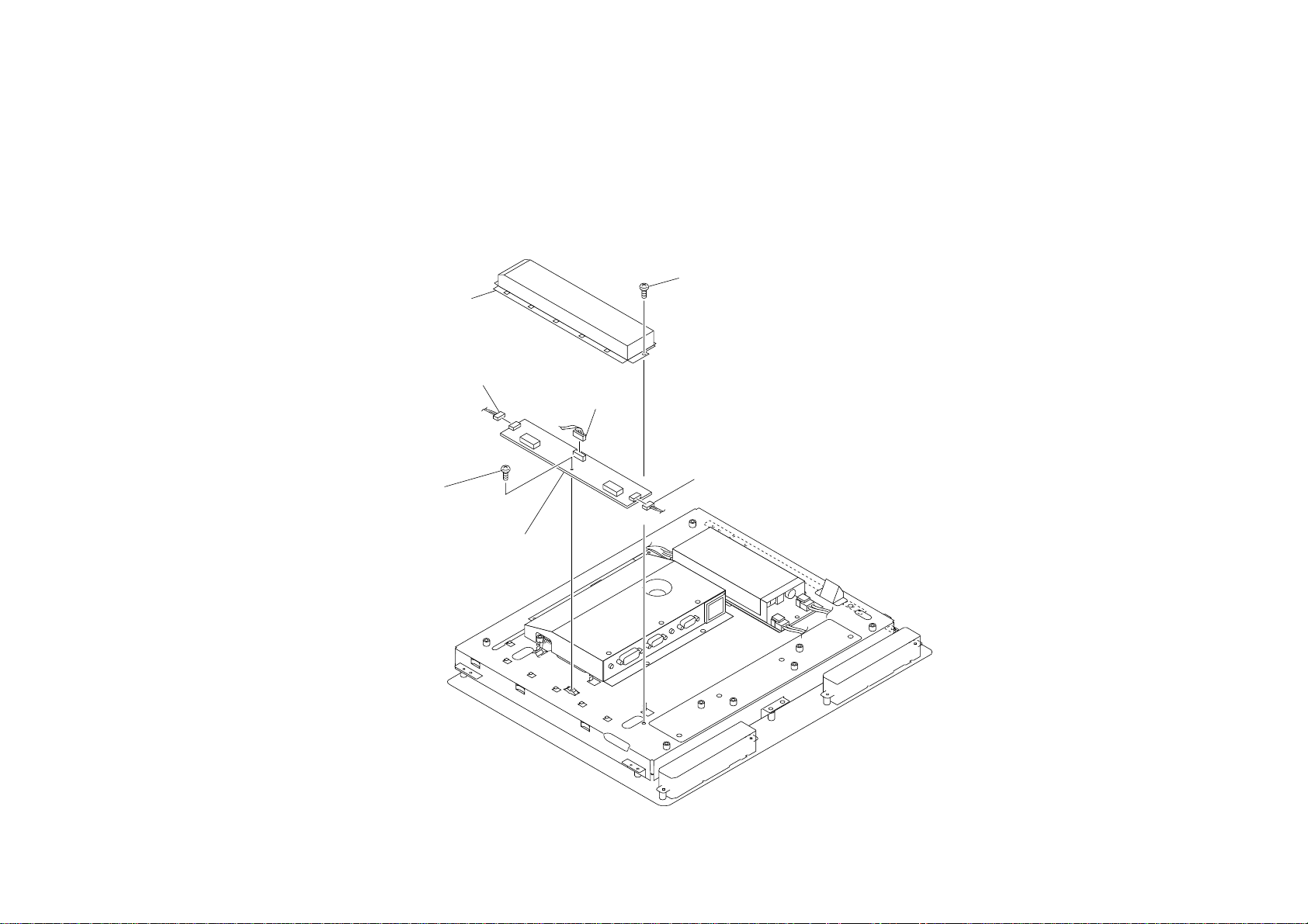
1-2. H BOARD REMOVAL
2 Three screws
(+PTP 3X8)
3 H Board
CN901
1 Connector
SDM-X72(E) 1-2
Page 8
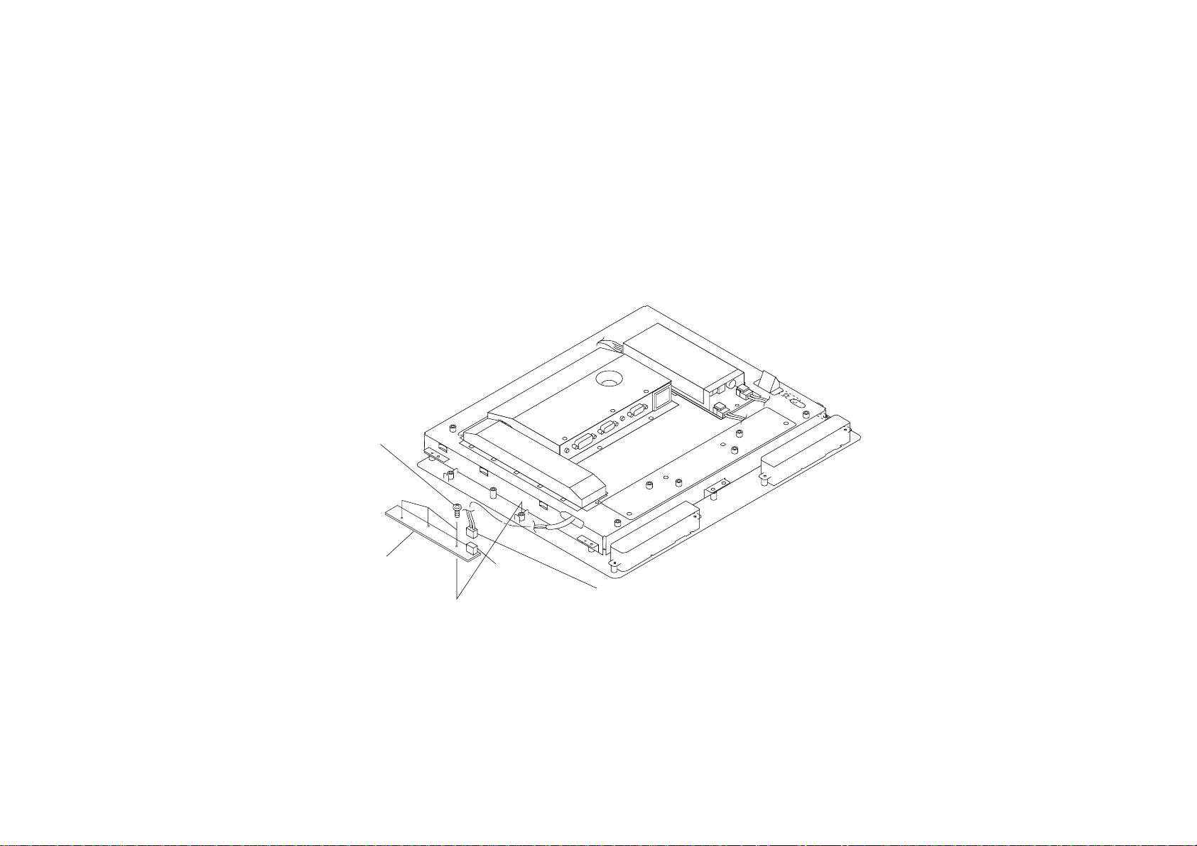
1-3. I BOARD REMOVAL
2 Invertor shield
3 Connector
CN03
1 Screw
(+PWH 3X6)
3 Connector
CN01
4 Screw
(+PWH 3X6)
3 Connector
CN02
5 I Board
SDM-X72(E) 1-3
Page 9
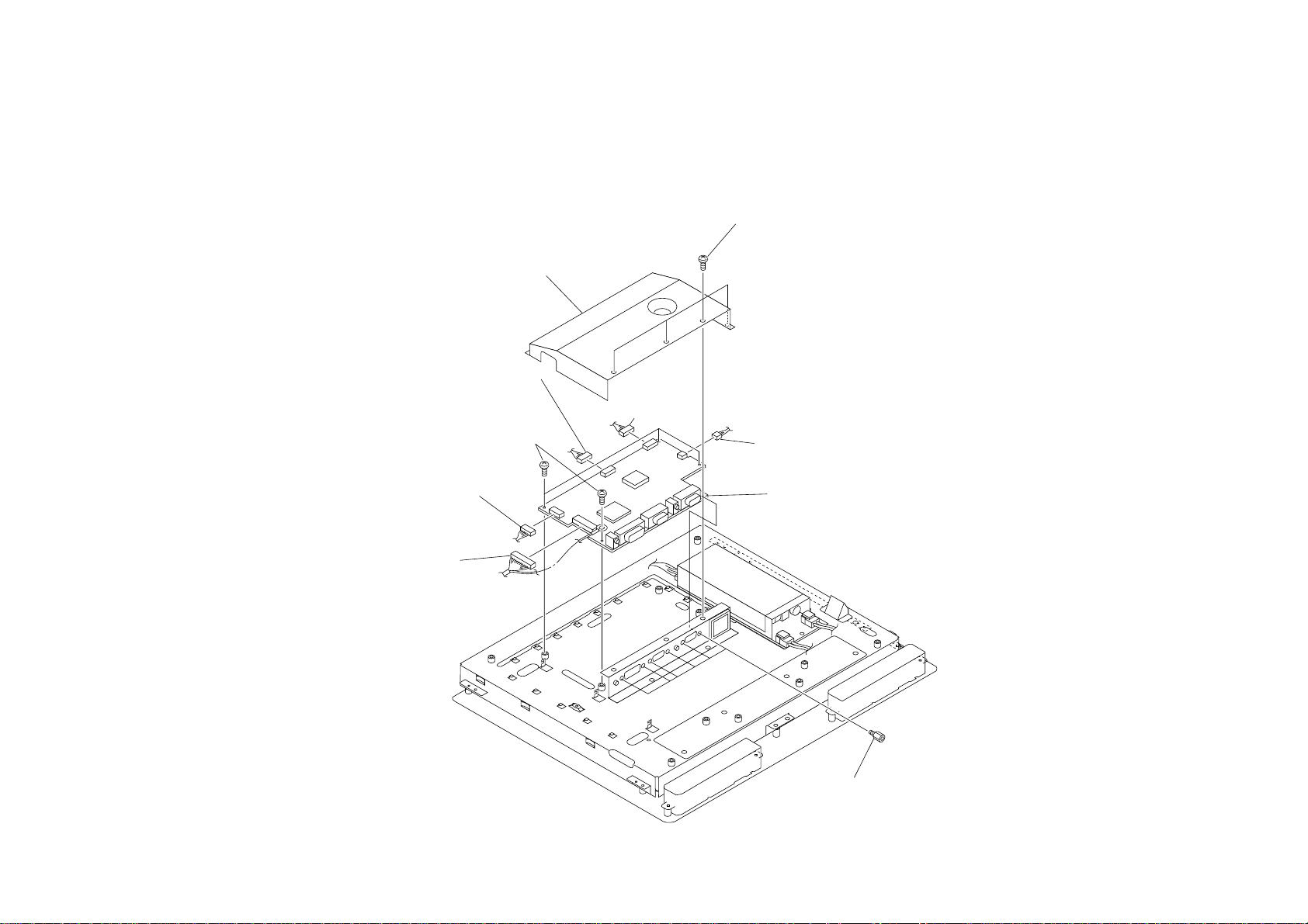
1-4. A BOARD REMOVAL
1 Four screws
(+PWH 3X6)
2 Interface shield
4 Connector
CN304
5 Four screws
(+PWH 3X6)
4 Connector
CN202
4 Connector
CN501
4 Connector
CN201
4 Connector
CN801
6 A Board
4 Six connector screws
SDM-X72(E) 1-4
Page 10
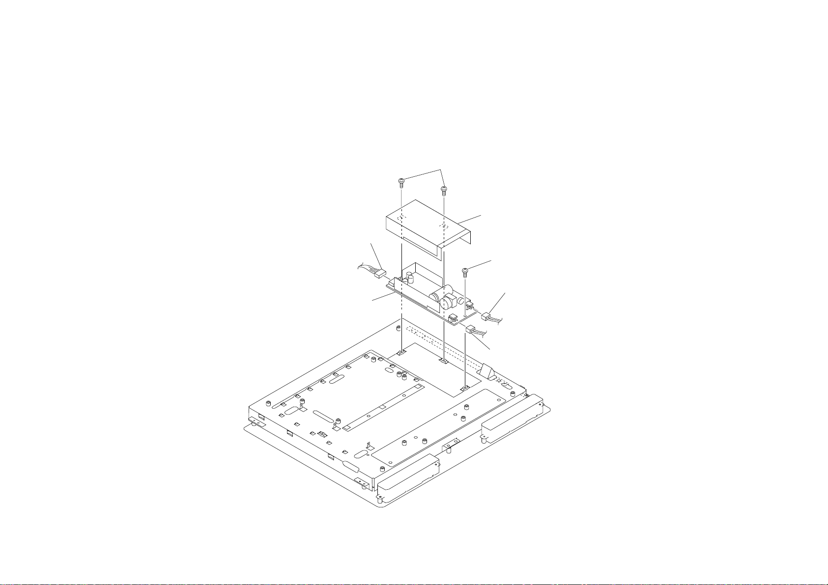
1-5. G BOARD REMOVAL
3 Connector
CN203
1 Two screws
(+PWH 3X6)
2 Power shield
4 Screw
(+PWH 3X6)
5 G Board
3 Connector
CN102
3 Connector
CN101
SDM-X72(E) 1-5
Page 11
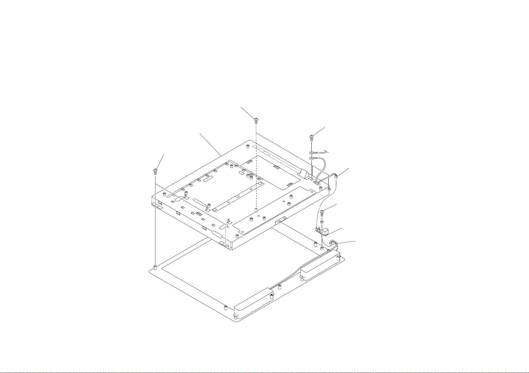
1-6. U BOARD AND LCD UNIT REMOVAL
3 Two screws
(+PTP 4X10)
3 Two screws
(+PTP 4X10)
4 LCD unit
2 Screw
(+PWH 3X6)
1 Connector
CN851
6 Screw
(+PTP 3X8)
7 U Board
5 Connector
CN852
SDM-X72(E) 1-6
Page 12
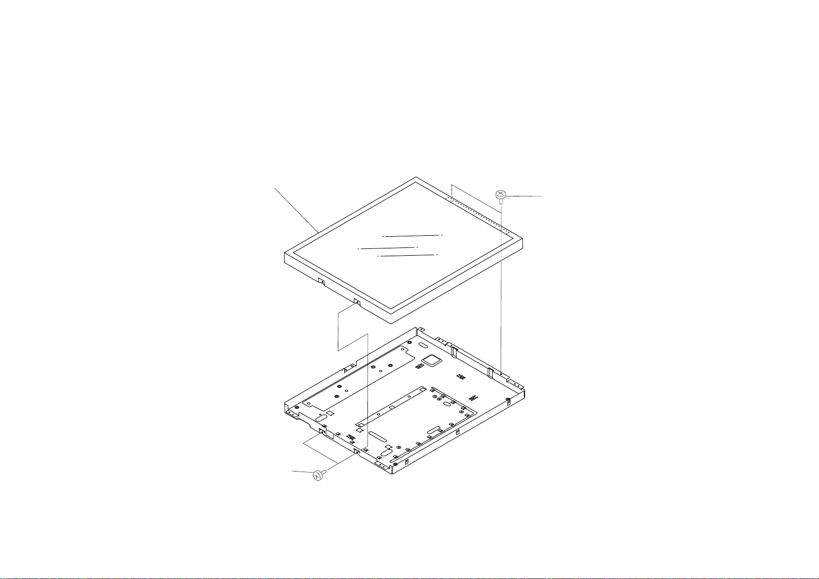
1-7. LCD PANEL REMOVAL
2 LCD panel
1 Two screws
(+P 3X4)
1 Two screws
(+P 3X4)
SDM-X72(E) 1-7
Page 13

SECTION 2
ADJUSTMENTS
2-1. Service Functions of Buttons in Front Panel
The following functions are available for servicing the set.
1. To display the model information
Press the MENU button for five seconds or more in the ordinary power-on state,
and the following information is displayed on the screen:
- Model name
- Serial number
- Manufactured year and week
This function is described in the instruction manual also.
2. To display ETI (Elapsed Time Indicator)
Press the OK button for five seconds or more in the ordinary power-on state, and
the cumulative power-on time excluding the power-off and power saving state is
displayed on the screen.
3. All mode recall
Press the POWER button with pressing the OK button in the power-off state, and
the user memory is completely cleared and the system is reset to the factory setting.
This reset is similar to RESET in the OSD menu, but differs from it in the
following:
- The NO SYNC AGING flag is cleared.
- LANGUAGE is set to ENGLIDH.
- INPUT is set to INPUT1: DVI-D.
5. To enter the service mode
Press the POWER button with pressing the UP (↑) and DOWN (↓)
buttons in the power-off state, and the system is set to the service mode. The service
mode will be explained later.
To exit from the service mode, turn off the power.
6. To copy EDID to the EEPROM and to clear ETI
Press the POWER button with pressing the UP (↑) and OK buttons in the
power-off state, and the data for the model information are copied to the EEPROM
for the internal microcontroller from EDID of INPUT2: HD15, and the model
information display is made correct.
When replacing the A board, this operation is required after writing EDID and at
the same time ETI is reset to 0.
7. To enter the ISP mode
Turn on the MAIN POWER switch with pressing the DOWN (↓) button in the
main-power-off state, and the system enters the ISP mode. The POWER LED goes
off, and both input LED's 1 and 2 light on, and the picture disappears, and any
button becomes invalid.
In the ISP mode, the internal software can be updated with an external personal
computer using a special fixture.
To cancel the ISP mode, turn off the MAIN POWER switch.
4. To set the NO SYNC AGING flag
Press the POWER button with pressing the UP (↑) button in the power-off
state, and the NO SYNC AGING flag is set. In this setting, when the input with no
input signal is selected, the system goes into the AGING MODE.
The NO SYNC AGING flag is held until it is cleared. To clear the NO SYNC
AGING flag, go into the service mode and then set the AGING MODE to OFF, or
execute the all mode recall.
SDM-X72(E) 2-1
Page 14
2-2. Uses of Service Mode
1. Turn off the power with the POWER button in the front panel. The red POWER
LED lights on.
2. Press the POWER button in the front panel with pressing the UP (↑) and
DOWN (↓) buttons, and the system enters the service mode.
When no signal is input to the selected input terminal, the following functions are
disabled.
3. Press the MENU button, and the main menu is displayed. Then go to page 2 of the
main menu with the UP (↑) or DOWN (↓) button, then select the MAINTAIN icon
on the bottom line, and then press the OK button.
4. In this menu screen, the version number and released date of the internal software
can be checked.
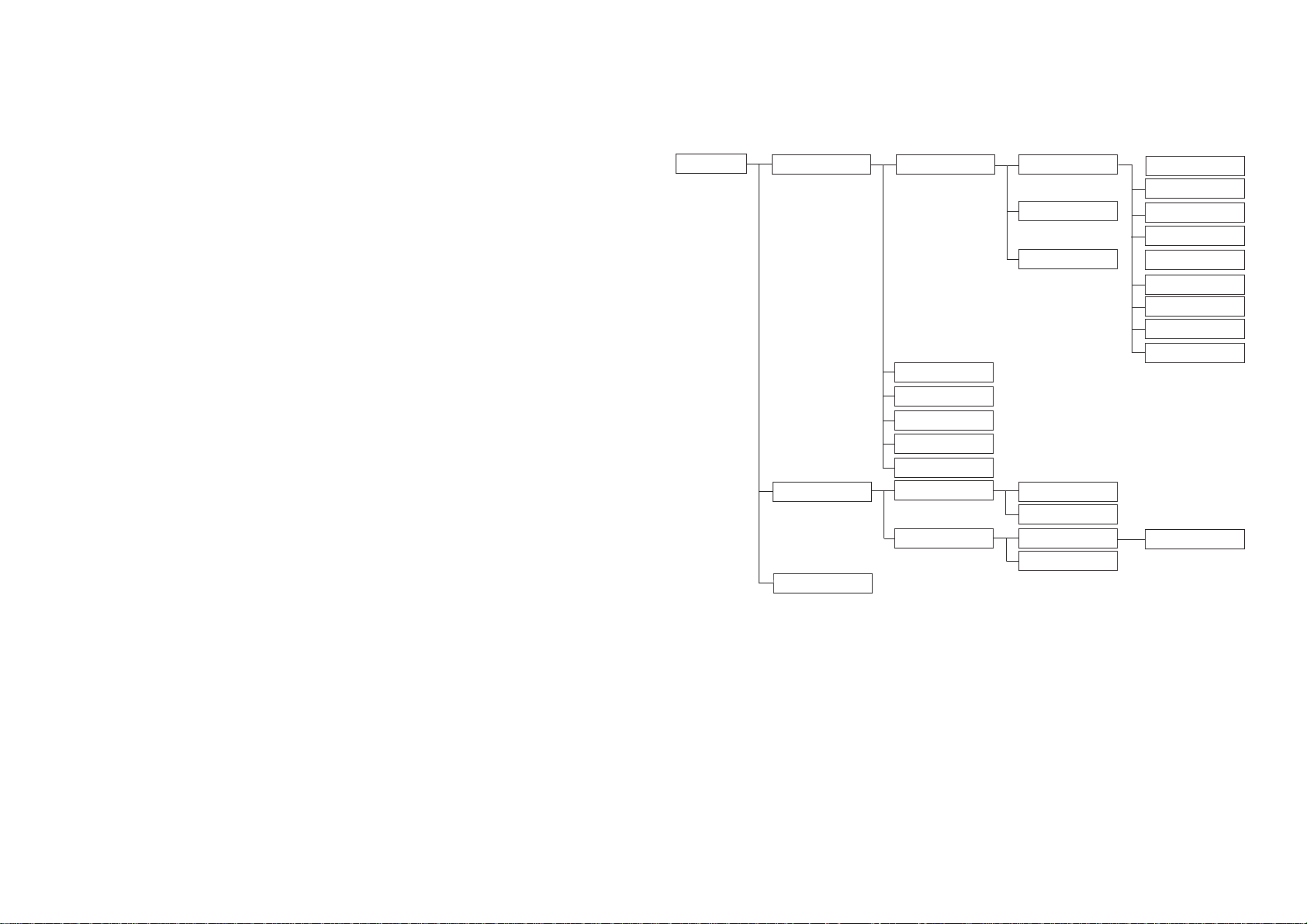
5. The structure of the MAINTAIN menu is shown below.
MAINTAIN
CONFIGURATI ON
CHIPS
EXIT
COLOR TEMP
INITIAL EEPROM
CLEAR ETI TIME
EEPROM TEST
RGB RESET
EXIT
AGING MODE
REGISTERS VALUE
9300K
6500K
EXIT
ON
OFF
CONTROL REG
EXIT
SUB-BRIGHTNESS
R
G
B
SUB-CONTRAST
R
G
B
EXIT
000~1FF
The operation procedure is basically same as that of the ordinary user controls.
The function of each menu is explained in next section.
SDM-X72(E) 2-2
Page 15

2-3. Functions of Service Mode
2-4. White Balance Adjustment
1. COLOR TEMP
This is used for the white balance adjustment at color temperature 9300 K and 6500
K. The adjustment requires to be done for every input (INPUT1: DVI-D, INPUT1:
HD15, or INPUT2: HD15) by switching the input. The adjustment data is stored into
the register for respective inputs.
2. INITIAL EEPROM
This sets the data of the EEPROM to the default data. This operation is not required
usually.
3. CLEAR ETI TIME
This resets the ETI (Elapsed Time Indicator) counter to 00000 H.
4. EEPROM TEST
This tests writing and reading of the EEPROM.
5. RGB RESET
This adjust the offset and gain of the input AD converter for the analog inputs
(INPUT1: HD15 and INPUT2:HD15). As these adjustments are common to both
inputs, perform them for either input. It is unnecessary for another input.
Execute the adjustments under the condition where the signal specified in "White
Balance Adjustment" is input.
6. AGING IN MODE
This sets and clears the NO SYNC AGING flag.
AGING MODE = ON: Sets the NO SYNC AGING flag.
AGING MODE = OFF: Clears the NO SYNC AGING flag.
When the NO SYNC AGING flag is set and the input with no input signal is
selected, the system goes into the AGING MODE. The NO SYNC AGING flag is
held until it is cleared. To clear the NO SYNC AGING flag, go into the service mode
and then set the AGINGN MODE to OFF, or execute the all mode recall.
< Preparation >
(1) Measurement point : Center of screen
(2) Measurement distance : 50 cm
(3) Measurement angle : 90°
(4) Color analyzer (Minolta CS-1000 or equivalent)
(5) Signal generator (Astro Design VG-828D or equivalent)
Be sure to calibrate the analog RGB output level with 75Ω termination.
1. Service mode setting
Enter the service mode referring to step 1 and 2 of Section 2-2.
2. Aging
Set the AGING MODE in the service mode to ON. Disconnect the signal input
terminal or select the input with no signal input, and the system goes into the
AGING MODE.
Execute aging for 30 minutes or more.
3. User control setting
Feed a signal to the selected input, and then execute reset in the menu screen. Then,
move the menu display position to avoid the measurement point. Or, set the
following for respective inputs.
BACKLIGHT (Brightness of backlight) = 100
CONTRAST = 70
BRIGHTNESS = 50
Menu display position = not center of screen (Avoid the measurement point.)
(The setting of the menu display position is common to respective inputs.)
ECO = OFF (The setting of ECO is common to respective inputs.)
Do not change the above setting until the white balance adjustment is completed.
7. CONTROL REG.
This can check the data of the internal registers. This operation is not required
usually.
SDM-X72(E) 2-3
Page 16

4. Analog RGB white balance adjustment
(1) Feed the signal listed below to INPUT2: HD15, and then select INPUT2: HD15.
Then execute RGB RESET in the service mode menu.
Signal timing
Pattern
Input level
(6) Adjust the SUB-BRIGHTNESS: R, G, and B.
Specifications are listed below.
x
0.313 ± 0.003
y
0.329 ± 0.003 10± 0.7
Brightness (cd/m2)
VESA 1280 * 1024 / 60Hz
Gray scale
0.73 Vp-p
(2) Feed the signal listed below to INPUT2: HD15.
Signal timing
VESA 1280 * 1024 / 60Hz
Pattern
All gray
Pattern
30 IRE (0.21 Vp-p)
(3) Select COLOR TEMP → 9300K in the service mode menu, and set the data
listed below as initial data for adjustment.
SUB-BRIGHTNESS
R
40
G
40
B
40
SUB-CONTRAST
R
148
G
148
B
143
(4) Adjust SUB-BRIGHTNESS: R, G, and B. Specifications are listed below.
x
0.283 ± 0.003
y
0.298 ± 0.003 12± 0.7
Brightness (cd/m2)
(7) After adjusting (4) and (6), write down the value of SUB-CONTRAST
and SUB-BRIGHTNESS.
(8) Feed the signal to INPUT1: HD15, and then select
INPUT1: HD15. Select COLOR TEMP → 9300K then 6500K in the service
mode menu, and enter the value written down in step (7) respectively.
5. Digital RGB white balance adjustment
(1) Feed the signal listed below to INPUT1: DVI-D.
Signal timing
VESA 1280 * 1024 / 60Hz
Pattern
All gray
Input level
30 IRE
(2) Select COLOR TEMP → 9300K in the service mode menu, and set the data
listed below as initial data for adjustment.
SUB-BRIGHTNESS
R
40
G
40
B
40
SUB-CONTRAST
R
132
G
132
B
132
(3) Adjust the SUB-BRIGHTNESS: R, G, and B. Specifications are listed below.
(5) Select COLOR TEMP → 6500K in the service mode menu, and set the data
listed below as initial data for adjustment.
SUB-BRIGHTNESS
R
40
G
40
B
40
SUB-CONTRAST
R
145
G
143
B
138
x
0.283 ± 0.003
y
0.298 ± 0.003 12± 0.7
Brightness (cd/m2)
SDM-X72(E) 2-4
Page 17

(4) Select COLOR TEMP → 6500K in the service mode menu, and set the data
listed below as initial data for adjustment.
2-5. Action after Replacing the LCD Panel and Board
SUB-BRIGHTNESS
R
40
G
40
B
40
SUB-CONTRAST
R
132
G
132
B
132
(5) Adjust the SUB-BRIGHTNESS: R, G, and B. Specifications are listed below.
x
0.313 ± 0.003
y
0.329 ± 0.003 12± 0.7
Brightness (cd/m2)
6. Setting for shipping
Turn off the power with the POWER button in the front panel. Check that the red
POWER LED lights on, and then execute the all mode recall. (press the POWER
button with pressing the OK button in the power-off state)
1. After replacing the LCD panel
(1) White balance adjustment. (Refer to Section 2-4.)
(2) CLEAR ETI TIME. (Refer to Section 2-3 step 3.)
(3) Check of picture and sound.
2. After replacing the A board
(1) White balance adjustment. (Refer to Section 2-4.)
(2) EDID writing.
As the write protection is not applied in this unit, it is possible to write data
with an ordinary writing fixture.
It is required to be written for INPUT1: DVI-D, INPUT1: HD15, and
INPUT2: HD15 respectively.
Take care that the data for DVI-D and HD15 terminals are different
from each other.
(3) EDID copy to the EEPROM and ETI clear. (Refer to Section 2-1 step 6.)
Be sure to perform them after EDID writing. After executing, check
that the correct model information is displayed. (Refer to Section 2-1 step 1.)
(4) Operation check of buttons and LED's in the front panel, and Check of
picture and sound for respective inputs.
3. After replacing the I board
(1) White balance adjustment. (Refer to Section 2-4.)
(2) Check of picture and sound.
4. After replacing the G board
(1) Operation check of the MAIN POWER switch.
(2) Check of picture and sound.
5. After replacing the H board
(1) Operation check of buttons and LED's in the front panel.
6. After replacing the U board
(1) Check of speaker sound.
(2) Check of headphone jack sound.
When connecting a plug to the headphone jack, confirm no sound from the
speakers.
SDM-X72(E) 2-5
Page 18

3-1. BLOCK DIAGRAMS
SECTION 3
DIAGRAMS
CN602
CN603
CN601
A BOARD
(INTERFACE)
CN301
IC307
IC603
IC401
I BOARD
(INVERTER)
BOARD
IC502
CN501
IC503
IC503
IC504
IC505
IC302
IC303
IC305
IC304
IC201
IC601
CN802
CN803
IC802
IC301
IC801
H BOARD
(IKEY BOARD)
CN801
G BOARD
(POWER)
U BOARD
(EARPHONE)
SDM-X72(E) 3-1
Page 19

3-2. CIRCUIT BOARDS LOCATION
A Board
I Board
H Board
G Board
U Board
SDM-X72(E) 3-2
Page 20

3-3. SCHEMATIC DIAGRAMS AND PRINTED WIRING BOARDS
Note:
• All capacitors are in µF unless otherwise noted. (pF: µµF)
Capacitors without voltage indication are all 50 V.
• Indication of resistance, which does not have one for rating electrical
power, is as follows.
Pitch: 5 mm
Rating electrical power 1/4 W (CHIP : 1/10 W)
• All resistors are in ohms.
• : nonflammable resistor.
• : fusible resistor.
∆ : internal component.
•
• : panel designation, and adjustment for repair.
• All variable and adjustable resistors have characteristic curve B, unless
otherwise noted.
• : earth-ground.
• : earth-chassis.
• When replacing the part in below table, be sure to perform the related
adjustment.
• All voltages are in V.
• Readings are taken with a 10 M digital multimeter.
• Readings are taken with a color-bar signal input.
• Voltage variations may be noted due to normal production tolerances.
•
• Circled numbers are waveform references.
• : B + bus.
• : B – bus.
: Can not be measured.
*
• Divided circuit diagram
One sheet of A board are circuit diagram is divided into eight sheets,
each having the code A-a to A-h. For example, the destination
ab1 on the code A-a sheet is connected to ab1 on the A-b sheet.
a b 1
Ref. No.
Circuit diagram division code
Note: The components identified by shading and
mark ! are critical for safety. Replace only
with part number specified.
Note: Les composants identifiés par un tramé et
une marque ! sont critiques pour la
sécurité. Ne les remplacer que par une pièce
portant le numéro spécifié.
SDM-X72(E) 3-3
Page 21

(1) Schematic Diagrams of A (a, b, c, d, e, f, g, h) Board
A
B
C
D
1
ag 1
afg2
2
0
0
0.2
0
43
+12V
7.7
7.5
7.7
1.2
1.2
7.7
2.5
10.8
10.6
2.5
1.2
0
I/F
0
1.0
0.2
7.5
+12V
10.6
+5V REG
+5V REG
98765
+5V
+5V
10
11
12
TO
G BOARD
CN203
13
14
15
E
F
G
H
10.8
+3.3V REG
+3.3V
+3.3V REG +3.3V REG
+5V
+3.3V
+5V
+3.3V
A
-
a
+5V
+2.5V REG
+5V
+2.5V
af 3
(POWER)
B-SS3627<J..>-A..-P1
• Divided circuit diagram
One sheet of A board are circuit diagram is divided into eight sheets,
each having the code A-a to A-h. For example, the destination
ab1 on the code A-a sheet is connected to ab1 on the A-b sheet.
I
a b 1
Ref. No.
Circuit diagram division code
SDM-X72(E) 3-4
Page 22

A
B
C
1
INPUT 1
DVI-D INPUT
(DIGITAL RGB)
2
ag 3
43
98765
10
11
12
bd 5
13
14
D
E
F
G
H
• Divided circuit diagram
One sheet of A board are circuit diagram is divided into eight sheets,
each having the code A-a to A-h. For example, the destination
ab1 on the code A-a sheet is connected to ab1 on the A-b sheet.
a b 1
Ref. No.
Circuit diagram division code
4.4
4.4
EEPROM
4.4
4.4
bc6
bg7
bc8
+5V
4.4
4.9
4.4
4.9
SW
4.9
4.8
0
bg 9
bg 10
A-b
(DVI AND DDC SWITCH IC)
B-SS3627<J..>-A..-P2
I
J
SDM-X72(E) 3-5
Page 23

A
1
2
43
98765
10
11
12
13
14
15
B
C
D
E
INPUT 2
HD 15 INPUT
(ANALOG RGB)
c g 1 1
c g 1 2
b c 8
b c 6
+5V
4.4
4.4
EEPROM
c g 16
0.6
+5V
0
+5V
0
+5V SW
F
G
H
I
J
K
INPUT 1
HD 15 INPUT
(ANALOG RGB)
c g 1 3
c g 1 4
+5V
4.4
4.4
AT2XC02-10SC
EEPROM
• Divided circuit diagram
One sheet of A board are circuit diagram is divided into eight sheets,
each having the code A-a to A-h. For example, the destination
ab1 on the code A-a sheet is connected to ab1 on the A-b sheet.
a b 1
Ref. No.
Circuit diagram division code
c g 1 5
c d 1 9
c d 1 7
c g 1 8
ANALOG SW
A-c
(ANALOG)
B-SS3627<J..>-A..-P3
SDM-X72(E) 3-6
Page 24

1
2
43
98765
10
11
12
13
14
15
A
B
C
D
E
+3.3V
+3.3V
+3.3V
+3.5V
cd19
df27
df26
df28
df29
df30
df31
df32
F
G
H
IC401
bd5
+2.5V
cd17
+2.5V
+3.3V
I
+2.5V
df20
dh21
dg22
dg23
dg24
dg25
GM5020
SCALER
de33
de34
de35
de36
de37
J
• Divided circuit diagram
One sheet of A board are circuit diagram is divided into eight sheets,
each having the code A-a to A-h. For example, the destination
K
ab1 on the code A-a sheet is connected to ab1 on the A-b sheet.
a b 1
Ref. No.
Circuit diagram division code
A
-
d
(SCALER)
B-SS3627<J..>-A..-P4
SDM-X72(E) 3-7
Page 25

A
B
C
1
de34
2
43
+3.3V +3.3V +3.3V
98765
10
11
12
13
de33
14
15
D
E
G
1.2
1.2
1.2
1.2
1.2
1.3
1.2
1.1
1.7
1.6
0
0
1.3
3.3
de35
de36 de37
3.3
3.3
3.3
0
0
SDRAM SDRAM SDRAM
1.8
0.7
2.2
0.6
0.8
1.0
1.0
1.0
0.6
1.0
0.1
0.9
0.3
0.8
1.0
1.0
1.2
1.2
1.2
1.2
1.2
1.3
1.2
1.1
1.7
1.6
1.3
3.3
3.3
3.3
3.3
1.8
0.7
2.2
0.6
0.8
1.0
1.0
1.0
0.6
0
0
0
0
1.0
0.1
0.9
0.3
0.8
1.0
1.0
1.2
1.2
1.2
1.2
1.2
1.3
1.2
1.1
1.7
1.6
1.3
3.3
0
0
3.3
3.3
3.3
1.8
0.7
2.2
0.6
0.8
1.0
1.0
1.0
0.6
1.0
0.1
0.9
0.3
0.8
1.0
1.0
0
0
F
H
A
-
e
(SDRAM)
I
• Divided circuit diagram
One sheet of A board are circuit diagram is divided into eight sheets,
each having the code A-a to A-h. For example, the destination
ab1 on the code A-a sheet is connected to ab1 on the A-b sheet.
a b 1
Ref. No.
J
Circuit diagram division code
B-SS3627<J..>-A..-P5
SDM-X72(E) 3-8
Page 26

A
1
2
43
98765
10
11
12
13
14
15
B
C
D
E
d f 3 0
a f 3
a f g 2
0
THC63LVDM83A
IC501
LVDS
3.8
0.7
+12V
0
0
+3.3V
d f 2 7
+5V
IC502
THC63LVDM83A
LVDS
1.3
1.3
1.2
1.3
1.2
1.2
1.3
1.3
1.3
1.2
TO LCD
1.2
1.2
1.1
1.3
1.2
1.3
1.3
1.1
1.2
1.2
1.3
+3.3V
f g 3 8
d f 2 0
G
H
d f 3 1
d f 2 8
F
d f 3 2
d f 2 6
d f 2 9
A
-
f
(LVDS)
I
• Divided circuit diagram
One sheet of A board are circuit diagram is divided into eight sheets,
each having the code A-a to A-h. For example, the destination
ab1 on the code A-a sheet is connected to ab1 on the A-b sheet.
J
a b 1
Ref. No.
Circuit diagram division code
B-SS3627<J..>A..-P6
SDM-X72(E) 3-9
Page 27

A
1
2
43
98765
10
11
12
13
14
15
B
C
D
E
EEPROM
4.9
+5V
4.9
0.6
dg24
dg25
0.3
0.2
0.2
0.2
4.5
4.5
4.9
0
0
bg9
fg38
cg12
4.9
4.9
4.9
0
4.9
4.9
1.1
1.2
0
0.1
0.1
0
MCU
4.9
4.9
4.9
4.9
4.9
4.9
4.9
0
3.1
0
0
4.9
4.9
4.9
4.9
0.1
0
0
afg2
4.9
0
bg4
bg10
cg11
cg14
cg16
cg18
0.1
ag1
cg13
cg15
gh39
G
H
F
4.9
0
TO
H BOARD
CN901
4.9
-9.0
0
-5.1
7.5
0
0
+5V
I / F
0
-9.0
0
4.9
4.8
4.8
0
4.8
0
dg22
gh40
bg7
0.5
0.5
10.9
4.9
3.0
3.3
dg23
5.2
4.9
TO
I BOARD
CN01
I
5.2
0
J
A
-
g
(MCU)
K
• Divided circuit diagram
One sheet of A board are circuit diagram is divided into eight sheets,
each having the code A-a to A-h. For example, the destination
ab1 on the code A-a sheet is connected to ab1 on the A-b sheet.
a b 1
Ref. No.
Circuit diagram division code
B-SS3627<J..> - A..-P7
SDM-X72(E) 3-10
Page 28

1
2
43
98765
10
11
12
13
14
15
A
B
C
D
E
INPUT2
AUDIO I N
INPUT1
AUDIO I N
AUDIO SW
dh21
5.8
5.8
5.7
5.8
AUDIO AMP
gh40
5.8
5.7
0
gh39
A
-
h
(AUDIO AND EARPHONE)
TO
U BOARD
CN851
G
B-SS3627<J..> - A..-P8
F
• Divided circuit diagram
One sheet of A board are circuit diagram is divided into eight sheets,
each having the code A-a to A-h. For example, the destination
ab1 on the code A-a sheet is connected to ab1 on the A-b sheet.
a b 1
Ref. No.
Circuit diagram division code
SDM-X72(E) 3-11
Page 29

A
1 2 34
A
B
C
[
MAIN CPU,SYSTEM IC,COLOR DEC,A/D CONV,3D COMB FILTER
— A BOARD —
1 2 34
A
B
]
C
<COMPONENT SIDE> <CONDUCTOR SIDE>
SDM-X72(E) 3-12
Page 30

(2) Schematic Diagram of H Board
1
2
A
B
C
D
43
TO
A(g)BOARD
CN303
98765
10
11
H
(KEY)
B-SS3627<J..>-H..
E
F
SDM-X72(E) 3-13
Page 31

H
[
]
KEY
— H BOARD —
<COMPONENT SIDE>
<CONDUCTOR SIDE>
SDM-X72(E) 3-14
Page 32

(3) Schematic Diagrams of I Board
A
B
C
D
E
F
G
1
5V
ICT53
5V
D06
BAS32
OP11
D04
BAS32
OP22
D05
BAS32
OP44
R41
ICT54
R42
2.7
PDRV_C
ICT58
R46
2.7
PDRV_A
C23
0.1u
C24
0.1u
C25
0.1u
2k
1k
R45
1k
2k
VIN
8.0
ICT55
6.0
Q1
2N7002LTA
VIN
8.0
6.0
Q8
2N7002LTA
ICT60
2
8.0
(INVERTOR)
43
CN01
7PIN
ICT56
Q10
BC817-25
ICT57
R04
8.0
10
P_C
Q11
BC807-25
Q16
BC817-25
R15
ICT59
10
P_A
Q17
BC807-25
R50
100k
0
8.4
1M
8.7
1M
8.2
2N7002LTA
0
2N7002LTA
0
2N7002LTA
R28
R29
1M
R30
I
TO
A (g) BOARD
CN202
5V
FB
1.2
Q24
0
2N7002LTA
Q25
Q26
Q27
PBC
VCC
VCC
GND
GND
GND
OFF
ADJ
D01
BAS32
OP1
D02
BAS32
OP2
D03
BAS32
OP4
D11
1SS355
D12
1SS355
D13
1SS355
F01
2A
D
63V
1
ICT19
2
3
4
6
0
5
7
ICT38
4.9
UDZSTE-175.6B
ICT51
C21
0.1u
ICT50
C22
0.1u
ICT52
C03
0.1u
YST-A186490
1
VP11
2
4
5
VP22
FB11
FB22
ZD01
R05
1M
R06
R07
1M
T06
VIN
ICT39
R12
47k
ICT42
R35
560
5V
C05
0.01u
R10
10k
ENA
CN07
2PIN
1
2
R36
390
1.2
ICT65
C07
ICT34
C04
1u
FB
C06
0.01u
ICT37
R09
22
ICT40
C09 1u
C08
1u
R14
681k
ICT44
R39
33k
D07
0
D21
100
10k
Q06
BC817-25
R08
R03
+5V
R11
100k
ICT43
0
Q02
2N7002LTA
0
Q03
8.8
2N7002LTA
ICT48
0
9.0
1M
8.9
Q04
2N7002LTA
ICT49
0
Q05
2N7002LTA
R01
ICT13
ICT63
7
D19
CY06
1SS226
22p
6
B
OP44
ICT64
R13
ICT35
C10 0.1u
1.2
1.2
2.1
C38
0.0015u
27k
5.1
4.8
5.0
ICT45
0.1
0.5
+12V
IC01
OZ9601S
1
2
3
4
5
6 15
2.5V
7
8
9
10 11
ICT46
R16
51k
D
F02
2A
63V
20
19
18
17
16
14
13
12
ICT29
C
+
ICT28
0.01u
C36
220u
ICT31
PDRV_A
PDRV_C
NDRV_D
C11
R17
30k
2.4
2.6
2.0
1.5
3.0
1.2
2.0
R20
15k
+12V
N_B
P_A
N_D
P_C
NDRV_B
ICT26
ICT33
R19
1M
PBC
2.4
8.0
2.4
8.0
NDRV_B
NDRV_D
C12
220p
J01
C13 0.01u
C15
0.1u
IC04
8958
1
IC05
8958
1
ICT23
ICT21
C40
10u
ICT8
ICT27
VP11
R18
20
R43
20
R21 62k
1SS355
ICT20
C14
D08
5.8
ICT66
C33
+
220u
35v
ICT22
N_B
N_D
D09
1SS355
D10
1SS355
YST-A186490
1
2
4
5
VP22VP11
ICT16
YST-A186490
1
2
5
5.8
98765
ICT18
ICT1
ICT25
IC02
8958
1
2.4
N_B
8.0
P_A
ICT24
VP1
IC03
8958
1
2.4
N_D
8.0
P_C
ICT17
T03
YST-A186490
1
VP1
VP2
FB1
FB2
T04
7
6
T05
674
7
2
C19
333p
6
4
5
ICT14
ICT15
ICT36
CY04
22p
ICT41
CY05
22p
10
T01
YST-A186490
ICT3
1
2
674
5
VP2VP1
C39
10u
ICT2
5.8
T02
YST-A186490
ICT6
1
2
674
5
5.8
CY03
ICT11
22p
D16
B
1SS226
R26
560
OP4
R27
ICT12
390
D20
B
1SS226
ICT47
D17
B
1SS226
R31
560
OP11 FB11
ICT30
ICT32
D18
B
1SS226
R33
560
OP22 FB22
ICT68
ICT9
CY01
22p
D14
B
1SS226
R22
560
OP1 FB1
ICT4
CY02
22p
D15
B
1SS226
R24
560
OP2 FB2
ICT7
ICT10
R32
390
ICT67
R34
390
ICT5
11
CN02
2PIN
1
TO LCD BACK LIGHT
2
R23
390
CN03
2PIN
1
TO LCD BACK LIGHT
2
R25
390
CN04
2PIN
1
TO LCD BACK LIGHT
2
CN05
2PIN
1
TO LCD BACK LIGHT
2
CN06
2PIN
1
TO LCD BACK LIGHT
2
12
13
H
B-SS3627<J..> - I..
SDM-X72(E) 3-15
Page 33

I
[
INVERTER
— I BOARD —
]
<COMPONENT SIDE>
<CONDUCTOR SIDE>
SDM-X72(E) 3-16
Page 34

(4) Schematic Diagram of U Board
1
2
A
TO
A (h)BOARD
CN801
B
C
D
43
HEAD PHONE
98765
10
11
E
F
G
U
(EARPHONE)
B-SS3627<J..>-U..
SDM-X72(E) 3-17
Page 35

U
[
EARPHONE
— U BOARD —
<COMPONENT SIDE>
<CONDUCTOR SIDE>
SDM-X72(E) 3-18
Page 36

(5) Schematic Diagrams of G Board
A
B
C
D
E
F
G
1
AC IN
100V
50/60Hz
2
MMBT4401
4A 250V
43
12
600uH
680k
0.33u
680k
ERZV10D621
680k
20k
0.01u
14.4
4.2
0
MMBT4403
1k
1k
14.2
0 14.4
LL4148-GS08
1u
20k
LL4148-GS08
510
75k
RLZTE-1118C
TLZ16C-GS08
4mH
470p
0.1u
47u 25v
D3SB60
MMBT4401
DAP008ADR2
0.1u
470p
0.1u
128.3
5.9
0.4
0.3
0.6
LL4148-GS08
0.001u
100u
450V
2N7002LT1
22k
14.5
51
100p
820k
820k
1M
820k
9.1M
100k
2.37k
BYV26E,133
120k
120k
120k
120k
BYV26E,133
1.5k
1N4935RL
1N4935RL
STB9NC60-1
TLZ24C-GS08
TLZ5V1B-GS08
120k
120k
100
5.7
TCET1104G
2.4
0.001u
0.001u
85.8
0.1
17A-U93
330
0.39
12.1
16CTQ100
0.001u
390
11.9
10.1
10
680p
10.8
DAS01A
2.4
220p
1k
100
100
0
2.4
98765
16CTQ100
0.001u
1.5k
1k
680u 25V
0.1u
39k
0
11
680u 25V
680u 25V
1.33k
0.1u
5.1k
12
+5V
100u 25V
0
0.01u
93.1k
48.7k51.1k
0.1u
51.1k
13
5
4
3
TO
A (a) BOARD
CN201
2
1
14
15
H
K
0.001u
22M
22M
0.001u
22M
22M
22M
0.001u
TLZ16C-GS08
0.1
LL4148-GS08
LL4148-GS08
51.1k
G(POWER)
I
J
B-SS3627<J..> - G..
SDM-X72(E) 3-19
Page 37

G
[
POWER SUPPLY
—G BOARD —
]
<COMPONENT SIDE>
<CONDUCTOR SIDE>
SDM-X72(E) 3-20
Page 38
• Items with no part number and no
description are not stocked because they
are seldom required for routine service.
• The construction parts of an assembled
part are indicated with a collation number
in the remark column.
• Items marked " * " are not stocked since
they are seldom required for routine
service. Some delay should be anticipated
when ordering these items.
The components identified ! marked are
critical for safety.
Replace only with the part number specified.
Les composants identifiés par la marque !
sont critiques pour la sécurité.
Ne les remplacer que par une pièce portant
le numéro spécifié.
SECTION 4
EXPLODED VIEWS
SDM-X72(E) 4-1
Page 39
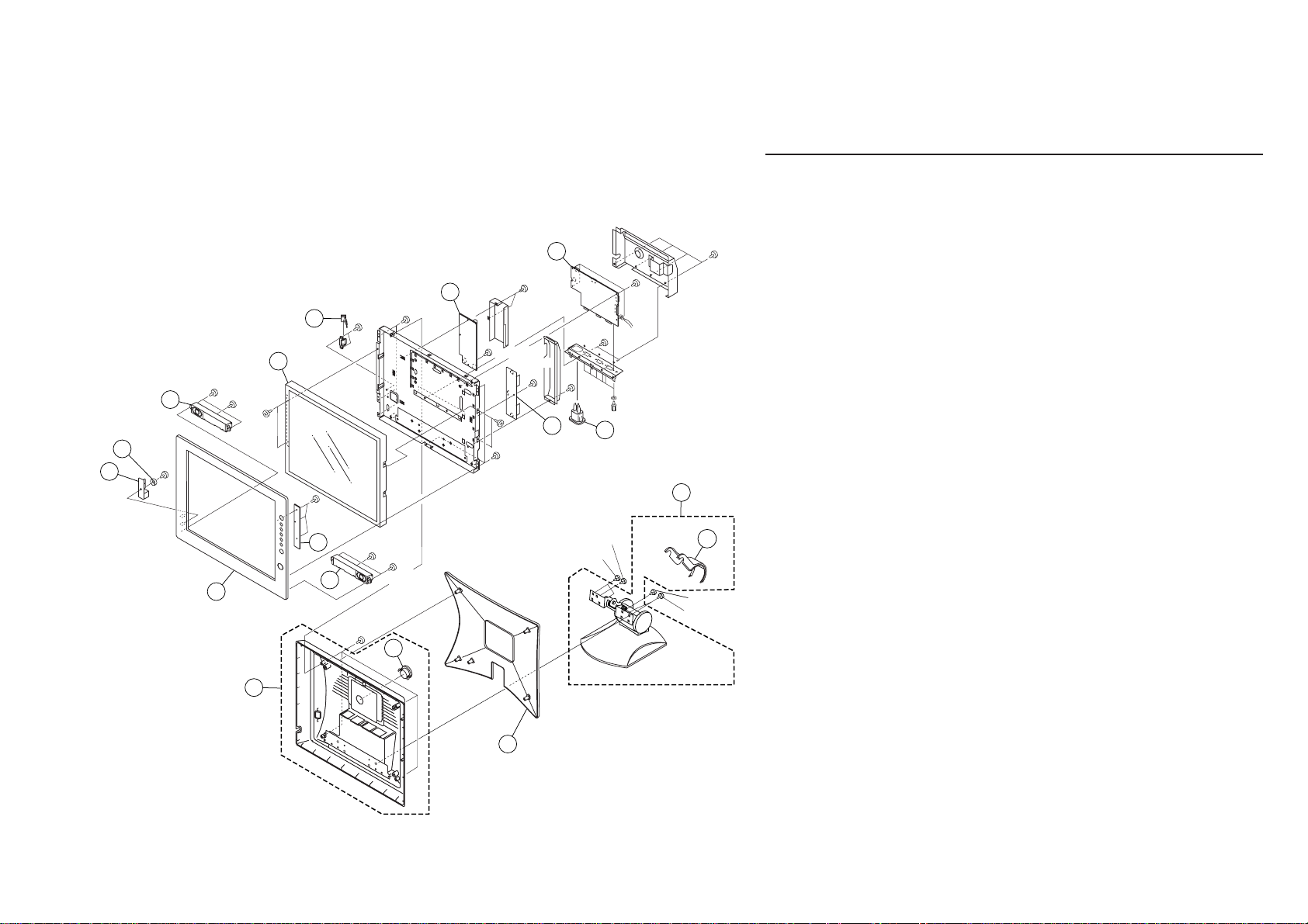
4-1. CHASSIS
+PWHTP 3X6
4
8
+PTP
3X8
7
+PTP
3X10
+P 3X4
6
2
REF.NO. PART NO. DESCRIPTION REMARK
1 4-090-557-01 COVER, REAR (GRAY)
(US/CND/AEP/CH)
4-090-557-11 COVER, REAR (BLACK)(US/CND/AEP)
14
+PWH 3X6
+PWH
3X6
+P 3X4
+PTP 4X10
+PWH
3X6
11
+PWH
3X6
+PWH
3X6
12
+PWH
3X5
13
+PP 4X10
+PWH 3X6
10
9
+PWH 3X6
15
+PTP
3X8
5
4
+PWH 3X12
+PTP 3X10
+PWHTP 3X6
+B 3X8
+PSW 4X10
16
+B 3X8
+PSW 4X10+PSW 4X10
3
2 X-4041-271-1 CABINET ASSY (GRAY) 3
(US/CND/AEP/CH)
X-4041-269-1 CABINET ASSY (BLACK) 3
(US/CND/AEP)
3 4-089-923-01 COVER, MINI DIN (GRAY)
(US/CND/AEP/CH)
4-089-923-11 COVER, MINI DIN (BLACK)
(US/CND/AEP)
4 1-825-215-11 BOX, SPEAKER
5 A-1401-985-A H BOARD, MOUNTED
6 X-4041-270-1 BEZEL ASSY (GRAY)
(US/CND/AEP/CH)
X-4041-268-1 BEZEL ASSY (BLACK)(US/CND/AEP)
7 A-1401-986-A
U BOARD, MOUNTED
8 4-093-038-01 WASHER
9 1-804-981-11 PANEL, LCD (M170EN05)
10 ! 1-786-460-11 SWITCH POWER
11 1-761-619-11 I BOARD, MOUNT (INVERTOR BOARD)
12 ! 1-417-348-11 INLET, AC
13 1-761-615-11 G BOARD, MOUNT (POWER BOARD)
14 A-1404-772-A A BOARD, MOUNTED
15 A-1604-259-A STAND ASSY (GRAY) 16
(US/CND/AEP/CH)
A-1604-255-A STAND ASSY (BLACK) 16
(US/CND/AEP)
1
16 4-089-996-01 COVER (REAR), ARM (GRAY)
(US/CND/AEP/CH)
4-089-996-11 COVER (REAR), ARM (BLACK)
(US/CND/AEP)
SDM-X72(E) 4-2
Page 40

4-2. PACKING MATERIALS
54 55 56 57 58 59
53
60 61
REF.NO. PART NO. DESCRIPTION REMARK
51 * 4-093-186-01 INDIVIDUAL CARTON (GRAY)
(US/CND/AEP/CH)
* 4-093-185-01 INDIVIDUAL CARTON (BLACK)
(US/CND/AEP)
52 * 4-093-187-01 CUSHION (LOWER)
53 * 4-092-765-01 BAG, PROTECTION
54 * 4-093-188-01 CUSHION (UPPER)
55 !
!
!
1-790-568-12 CORD SET, POWER (U/C)
1-765-719-11 CORD SET, POWER (AEP)
1-827-087-11 CORD SET, POWER (CH)
56 1-824-952-11 CORD WITH CONNECTOR(15P DSUBX2)
57 1-824-963-11 CORD WITH CONNECTOR
58 1-824-598-11 CABLE, DVI-D
59 4-093-065-11 MANUAL, INSTRUCTION (U/C)
4-089-157-21 MANUAL, INSTRUCTION (AEP)
4-089-157-32 MANUAL, INSTRUCTION (CH)
60 1-796-619-11 DISC, CD-ROM
52
51
61 * 4-093-235-01 LABEL, INFORMATION (GRAY)
(US/CND/AEP/CH)
* 4-093-235-11 LABEL, INFORMATION (BLACK)
(US/CND/AEP)
SDM-X72(E) 4-3
Page 41

NOTE:
The components identified ! marked are
critical for safety.
Replace only with the part number specified.
SECTION 5
ELECTRICAL PARTS LIST
• All variable and adjustable resistors have
characteristic curve B, unless otherwise
noted.
Les composants identifiés par la marque !
sont critiques pour la sécurité.
Ne les remplacer que par une pièce portant
le numéro spécifié.
When indicating parts by reference
number, please include the board name.
• Items marked " * " are not stocked since
they are seldom required for routine
service. Some delay should be anticipated
when ordering these items.
RESISTORS
• All resistors are in ohms
• F : nonflammable
SDM-X72(E) 5-1
Page 42

No. # Board Type !/*Ref.No. Part No. Descrption Remarks-1 Remarks-2 Difference
1 A FUSE F201 1-576-704-11 FUSE 7A 125V
!
2 A IC IC201 6-703-630-01 IC BA9741F
3 A IC IC204 6-702-889-01 IC SI-3033KS-TL
4 A IC IC205 6-702-940-01 IC XC6203E332PR
5 A IC IC206 6-703-152-01 IC LD1085DT
6 A IC IC208 6-702-940-01 IC XC6203E332PR
7 A IC IC301 6-702-994-01 IC MTV412MV128
8 A IC IC303 8-759-672-79 IC M24C02-WMN6T(A)
9 A IC IC304 8-759-672-79 IC M24C02-WMN6T(A)
10 A IC IC305 8-759-672-79 IC M24C02-WMN6T(A)
11 A IC IC401 6-703-171-01 IC GM5020
12 A IC IC603 8-759-541-25 IC M52758P
13 A IC IC801 6-702-887-01 IC TDA7496L
14 G DIODE D130 8-719-510-51 DIODE D3SB60F
15 G DIODE D201 6-500-359-01 DIODE STPS20H100CT
16 G DIODE D202 6-500-359-01 DIODE STPS20H100CT
17 G IC IC101 6-702-918-01 IC DAP008ADR2
18 G IC IC251 6-702-917-01 IC DAS001
19 G TRANSISTOR Q101 6-550-394-01 TRANSISTOR STB9NC60-1
20 H DIODE D909 6-500-388-01 DIODE L-934SYC
21 H DIODE D910 6-500-388-01 DIODE L-934SYC
22 H SWITCH S901 1-786-426-11 SWITCH, TACTILE
23 H SWITCH S902 1-786-426-11 SWITCH, TACTILE
24 H SWITCH S903 1-786-426-11 SWITCH, TACTILE
25 H SWITCH S904 1-786-426-11 SWITCH, TACTILE
26 H SWITCH S905 1-786-426-11 SWITCH, TACTILE
27 H SWITCH S906 1-786-426-11 SWITCH, TACTILE
28 H SWITCH S907 1-786-426-11 SWITCH, TACTILE
29 I FUSE F1 1-576-410-21 FUSE, CHIP
30 I FUSE F2 1-576-410-21 FUSE, CHIP
!
!
31 I IC IC1 6-702-916-01 IC OZ960S
SDM-X72(E) 5-2
Page 43

No. # Board Type !/*Ref.No. Part No. Descrption Remarks-1 Remarks-2 Difference
32 I IC IC2 6-702-915-01 IC SI4532DY
33 I IC IC3 6-702-915-01 IC SI4532DY
34 I IC IC4 6-702-915-01 IC SI4532DY
35 I IC IC5 6-702-915-01 IC SI4532DY
SDM-X72(E) 5-3
Page 44

9-878-803-01
Sony Corporation
Sony Technology Center
Technical Services
Service Promotion Department
English
2003AJ74WEB-1
Printed in USA
© 2003.1
Page 45

HISTORY INFORMATION FOR THE FOLLOWING MANUAL:
SERVICE MANUAL
SDM-X72
US Model
Canadian Model
AEP Model
Chinese Model
DL1
CHASSIS
ORIGINAL MANUAL ISSUE DATE: 1/2003
ALL REVISIONS AND UPDATES TO THE ORIGINAL MANUAL ARE APPENDED TO THE END OF THE PDF FILE.
REVISION DATE REVISION TYPE SUBJECT
1/2003 No revisions or updates are applicable at this time.
Design and specications are subject to change without notice.
TFT LCD COLOR COMPUTER DISPLAY
9-878-803-01
Page 46

PRINTING THE SERVICE MANUAL
The PDF of this service manual is not designed to be printed from cover to cover. The pages vary in size, and must therefore be printed in sections
based on page dimensions.
NON-SCHEMATIC PAGES
Data that does NOT INCLUDE schematic diagrams are formatted to 8.5 x 11 inches and can be printed on standard letter-size and/or A4-sized paper.
SCHEMATIC DIAGRAMS
The schematic diagram pages are provided in two ways, full size and tiled. The full-sized schematic diagrams are formatted on paper sizes between
8.5” x 11” and 18” x 30” depending upon each individual diagram size. Those diagrams that are LARGER than 11” x 17” in full-size mode have been
tiled for your convience and can be printed on standard 11” x 17” (tabloid-size) paper, and reassembled.
TO PRINT FULL SIZE SCHEMATIC DIAGRAMS
If you have access to a large paper plotter or printer capable of outputting the full-sized diagrams, output as follows:
1) Note the page size(s) of the schematics you want to output as indicated in the middle window at the bottom of the viewing screen.
2) Go to the File menu and select Print Set-up. Choose the printer name and driver for your large format printer. Con fi rm that the printer settings
are set to output the indicated page size or larger.
3) Close the Print Set Up screen and return to the File menu. Select “Print...” Input the page number of the schematic(s) you want to print in the
print range window. Choose OK.
TO PRINT TILED VERSION OF SCHEMATICS
Schematic pages that are larger than 11” x 17” full-size are provided in a 11” x 17” printable tiled format near the end of the document. These can be
printed to tabloid-sized paper and assembled to full-size for easy viewing.
If you have access to a printer capable of outputting the tabloid size (11” x 17”) paper, then output the tiled version of the diagram as follows:
1) Note the page number(s) of the schematics you want to output as indicated in the middle window at the bottom of the viewing screen.
2) Go to the File menu and select Print Set-up. Choose the printer name and driver for your printer. Con fi rm that the plotter settings are set to output
11” x 17”, or tabloid size paper in landscape (
3) Close the Print Set Up screen and return to the File menu. Select “Print...” Input the page number of the schematic(s) you want to print in the
print range window. Choose OK.
TO PRINT SPECIFIC SECTIONS OF A SCHEMATIC
To print just a particular section of a PDF, rather than a full page, access the Graphics Select tool in the Acrobat Reader tool bar.
1) To view the Graphics Select Tool, press and HOLD the mouse button over the Text Select Tool which looks like:
This tool will expand to reveal to additional tools.
Choose the Graphics Select tool by placing the cursor over the button on of the far right that looks like:
) mode.
T
2) After selecting the Graphics Select Tool, place your cursor in the document window and the cursor will change to a plus (+) symbol. Click and
drag the cursor over the area you want to print. When you release the mouse button, a marquee (or dotted lined box) will be displayed outlining
the area you selected.
3) With the marquee in place, go to the fi le menu and select the “Print...” option. When the print window appears, choose the option under the section
called “Print Range” which says “Selected Graphic”.
Select OK and the output will print only the area that you outlined with the marquee.
(continued >)
Page 47

ON-SCREEN SEARCH OPTION
All of the text within the service manual PDF is content searchable. This means that you can enter any text, word, phrase or reference number that
appears in the manual, and the PDF software will search, fi nd and move the cursor to the location where you requested text fi rst appears. This feature
can be particularly useful in locating components on a specifi c schematic or printed wire circuit board (PWB) diagrams.
Follow these steps to effectively locate a component on a schematic diagram:
1) Locate the schematic you want to search by clicking on the corresponding bookmark on the left side of the screen. The view on the right of the
screen will then jump to the desired schematic page.
2) Magnify the diagram to at least 400% before conducting a component search. This will enable you to easily view the reference number when
it is highlighted on screen. To do this, click on the magnifying glass button on the tool bar at the top of the screen. Move the cursor over the
diagram and RIGHT click you mouse. Select the 400% magnifi cation option on the pop-up menu. Click on the button with the icon of the open
hand to deactivate the magnifi cation tool
3) Search the diagram (or the entire manual) by clicking on the binocular button tool at the top of the screen. The “Find” window will appear and
allow you to type in your desired text. Type in a reference designator, such as R502, and click on the “Find” button. If the component is not on the
diagram, but is listed anywhere else in the manual, the cursor will jump to the fi rst location the text is found in the fi le. To fi nd another instance of
that same text, click on the binocular button again and select “Find Again.”
 Loading...