

Page 1

SCPH-9000 SERIES
SCPH-9000
3rd Edition
SERIES
Japan Model
SCPH-9000
US/Canada Model
SCPH-9001
Australia Model
SCPH-9002A
UK Model
SCPH-9002B
AEP Model
SCPH-9002C
Asia Model
SCPH-9003
Sony Computer Entertainment Inc.
Customer Service Dept.
1999. 5 Printed in Japan © 9-927-069-03
Reproduction Prohibited
Registered No.
Sony Computer Entertainmant Europe
Page 2

Reproduction Prohibited
SCPH-9000 SERIES
Notice
Manual copylight 1999 by Sony Computer Entertainment Inc. All rights.
Reproduction without the expressed written permission of Sony
Computer Entertainment Inc. is strictly prohibited.Commercial use or
rental prohibited.
Revisions
Design and specifications are subject to change with out notice.
SCEI. Customer Service Dept. Service web site PS SERVICE PLAZA
(http:// svc. scei. co. jp) should be used together with this manual.
Attention
Ordering replacement components.
SCEI. Customer Service Dept. Parts-Group is received PlayStationrepair parts order. When you want to get them. Please accesses to
this E-mail address. (sec_parts@ hq. scei. sony. co. jp)
TABLE OF CONTENTS
1. SPECIFICATIONS ..................................................................2
2. EXPLODED VIEW ..................................................................3
3. ADJUSTMENT
3-1.Adjustment and Check Specification .............................................4
4. NOTICE .......................................................................................4
5. BLOCK DIAGRAMS..............................................................5
6. PRINTED WIRING BOARDS
AND SCHEMATIC DIAGRAMS
• Printed Wiring Board [PU-23 Board (-11/-21/-31/-41/-51)] ...........8
• Schematic Diagram [PU-23 Board (1/4) (-11/-21/-31/-41/-51)] .....9
• Schematic Diagram [PU-23 Board (2/4) (-11/-21/-31/-41/-51)] ...10
• Schematic Diagram [PU-23 Board (3/4) (-11/-21/-31/-41/-51)] ...11
• Schematic Diagram [PU-23 Board (4/4) (-11/-21/-31/-41/-51)] ...12
• Power Block (1-468-366-11) .........................................................14
• Power Block (1-468-365-11) .........................................................15
• Power Block (1-468-303-13) .........................................................16
• Power Block (1-468-243-11) .........................................................17
7. ELECTRICAL PARTS LIST
• PU-23 Board ..................................................................................18
• Power Block...................................................................................23
— 1 —
Page 3

Reproduction Prohibited
SCPH-9000 SERIES
SECTION 1
SPECIFICATIONS
SCPH-9000
General
Power requirements
100 V AC, 50/60 Hz
Power consumption
9 W
Dimensions
270 × 60 × 188 mm (w/h/d)
Mass
1.2 kg
SCPH-9001
General
Power requirements
120 V AC, 60 Hz
Power consumption
17 W
Dimensions
270 × 60 × 188 mm (w/h/d)
Mass
1.3 kg
Laser diode properties
•Material : GaAlAs
•Wavelength : 1 = 780 nm
•
Emission duration : Continuous
•
Laser output : Less than 44.6 µW
(measured at a distance of
200 mm from the lens surface
on the optical pick-up block)
Inputs/ Outputs on the front
Controller ports (2)
Memory card slots (2)
Laser diode properties
•Material : GaAlAs
•Wavelength : 1 = 780 nm
•
Emission duration : Continuous
•
Laser output : Less than 44.6 µW
(measured at a distance of
200 mm from the lens surface
on the optical pick-up block)
Inputs/ Outputs on the front
Controller ports (2)
Memory card slots (2)
I
nputs/Outputs on the rear
Serial I/O port (1)
Outputs on the rear
AV Multi out port
Supplied accessories
AC power cord (1)
A/V connecting cable (1)
Analog controller (1)
Instruction manual (1)
I
nputs/Outputs on the rear
Serial I/O port (1)
Outputs on the rear
AV Multi out port (1)
Supplied accessories
AC power cord (1)
A/V connecting cable (1)
Analog controller (1)
Instruction manual (1)
SCPH-9002/A/B/C
General
Power requirements
220-240 V AC, 50 Hz
Power consumption
10 W
Dimensions
270 × 60 × 188 mm (w/h/d)
Mass
1.2 kg
SCPH-9003
General
Power requirements
110-240 V AC, 50/60 Hz
Power consumption
11 W
Dimensions
270 × 60 × 188 mm (w/h/d)
Mass
1.2 kg
Laser diode properties
•Material : GaAlAs
•Wavelength : 1 = 780 nm
•
Emission duration : Continuous
•
Laser output : Less than 44.6 µW
(measured at a distance of
200 mm from the lens surface
on the optical pick-up block)
Inputs/ Outputs on the front
Controller ports (2)
Memory card slots (2)
Inputs/Outputs on the rear
Serial I/O port (1)
Laser diode properties
•Material : GaAlAs
•Wavelength : 1 = 780 nm
•
Emission duration : Continuous
•
Laser output : Less than 44.6 µW
(measured at a distance of
200 mm from the lens surface
on the optical pick-up block)
Inputs/ Outputs on the front
Controller ports (2)
Memory card slots (2)
Outputs on the rear
AV Multi out port (1)
Supplied accessories
AC power cord (1)
A/V connecting cable (1)
(except for the SCPH-9002B)
Analog controller (1)
Instruction manual (1)
RFU adaptor (1)
(for SCPH-9002B)
AV-connector plug (1)
(for SCPH-9002C)
Inputs/Outputs on the rear
Serial I/O port (1)
Outputs on the rear
AV Multi out port (1)
Supplied accessories
AC power cord (1)
A/V connecting cable (1)
Analog controller (1)
Adapter Conversion 2P (1)
Instruction manual (1)
— 2 —
Design and specifications are subject to change without notice.
Page 4

Reproduction Prohibited
CAUTION
The components identified by
mark ! or dotted line with mark.
! are critical for safety.
Replace only with part number
specified.
CAUTION :
Use of controls or adjustments or performance
of procedures other than those specified herein
may result in hazardous radiation exposure.
SCPH-9000 SERIES
SECTION 2
EXPLODED VIEW
UPPER X-3949-786-1 CABINET(UPPER) ASSY (9000) (9003)
UPPER X-3949-787-1 CABINET(UPPER) ASSY (9001)
UPPER X-3949-788-1 CABINET(UPPER) ASSY (9002)
INSU 3-965-376-01 INSULATOR
AEM 8-820-067-01 DEVICE OPTICAL KSM-440AEM
A
PM 1-945-377-31 HARNESS (PM-86)
FFC A-6775-347-A CABLE BLOCK ASSY, FLAT
PP 1-959-132-13 HARNESS (PP-169)
STOPPER 3-052-440-02 STOPPER, HARNESS
PSB 1-468-366-11 POWER BLOCK (9000)
PSB 1-468-365-11 POWER BLOCK (9001)
PSB 1-468-303-13 POWER BLOCK (9002)
PSB 1-468-243-11 POWER BLOCK (9003)
Screw
+BV 3X12
Screw
+BV 3X12
Screw
+BV 3X12
Screw
+BV 3X12
P 3-972-494-01 CUSHION P
SUB X-3949-789-1 FRAME ASSY, SUB
PU-23 A-6791-936-A MOUNTED CIRCUIT BOARD, PU-23 (9000)
PU-23 A-6791-939-A MOUNTED CIRCUIT BOARD, PU-23 (9001)
PU-23 A-6791-937-A MOUNTED CIRCUIT BOARD, PU-23 (9002)
PU-23 A-6791-938-A MOUNTED CIRCUIT BOARD, PU-23 (9003)
L-SHIELD 3-056-229-01 SHIELD (LOWER)
TERMINAL 1-694-473-12 TERMINAL BOARD (FRONT)
S-FRONT 3-052-152-02 SHIELD (FRONT)
Screw
+BV 3X12
— 3 —
A
Screw
+BV 3X14
Screw
+BV 3X14
LOWER 3-056-223-01 CABINET (LOWER)
CAUTION : for SCPH9001
CAUTION SERIAL No. LABEL (3- 969- 533- 11)
must be putted on the top of TERMINAL BOARD
according to the standard of UL1492.
Page 5

Reproduction Prohibited
SECTION 3
SCPH-9000 SERIES
SECTION 4
ADJUSTMENT
3-1. Test Specification
RF Level 0.90 to 1.35 Vp-p (Test point : Between CL704 and CL710)
• RF signal waveform (Eye pattern)
VOLT/DIV
TIME/DIV
0.90 to 1.35 Vp-p
0 V
Use SCD-2700 DISC when measured RF level.
Use an oscilloscope with input impedance over 10 M Ω
RF Jitter Less 9.0 nS (Measuring with KSM- 6135S JITTER METER.)
Less 27.0 nS (Measuring with KSM- 6235S JITTER METER.)
PP Level 1.1 ±0.6 Vp-p (Test point : Between CL776 and CL710)
Use LPF (fc = 10 kHz)
Tracking Level 1.3 ±0.6 Vp-p (Test point : Between CL709 and CL710 )
Caution Vc Line (CL710) do not wire to other lines together.
: 0.2 V
: 500 nS
NOTICE
Circuit Notes :
: B+ Line.
Voltages are measured with a Digital Multimeter. (Input impedance over 10 MΩ.)
Waveforms easured with an Oscilloscope DC coupled.
Semiconductors.
In each case. u : µ, for example ; uA : µA, uPA : µP A, uPB : µPA, uPC : µPA.
Unit Descriptions :
Capacitors.
Unit of Capacitor is µF and pF, for example ; uF : µF, pF : µµF.
Resisters.
Unit of Resistor is Ω.
Inductance.
Unit of Inductance is µH and mH
Caution. Vc Line (CL710) do not make common use with GND line.
Test Point for PU-23 Board.
CL710
CL709
CL704
CL727
CL760
R717
CL704
15
14
R723
C716
C729
52
CL727
FB702
53
C721
CL784
FB701
FB704
C725
C701
CL791
R793
CL785
C726
1
CL790
C761
CL709
R770
C718
CN701
CL787
C741
R775
CL776
CL711
C720
14
CL776
59
CL777
CL775
CL779
R732
CL786
FB703
CL316
L701
C739
Q701
R733
R727
CL710
13 15
CL780CL778
R747
CL728
HA002
CL706
C738
CL708
R750
CL706
C742
CL728
Parts List Notes:
Due to standardization, Parts may be different from the parts described in the diagrams or used on
the Set.
Attention :
Dielectric voltage withstand test and Insuiation resistance test.
After repair complete. Dielectric voltage withstand test and Insulation resistance test to be conducted according to the regulation of IEC-65 EN60065 or UL1492 or .
About replacement of Optical Device.
Before exchanging the Optical Device, Check the RF level, Jitter, Eye pattern, Focus gain and
Tracking error. When Optical Device is meet the specification, Playback the PS1 testing disc
“QA-DISC” or “AGING DISC” for checking the double speed and sled mechanism ability.
Optical Device should have to no exchange when spacification and ability are satisfied.
1-674-987-
1-674-987-
11 12
— 4 —
Page 6
Reproduction Prohibited
PU-23 BOARD
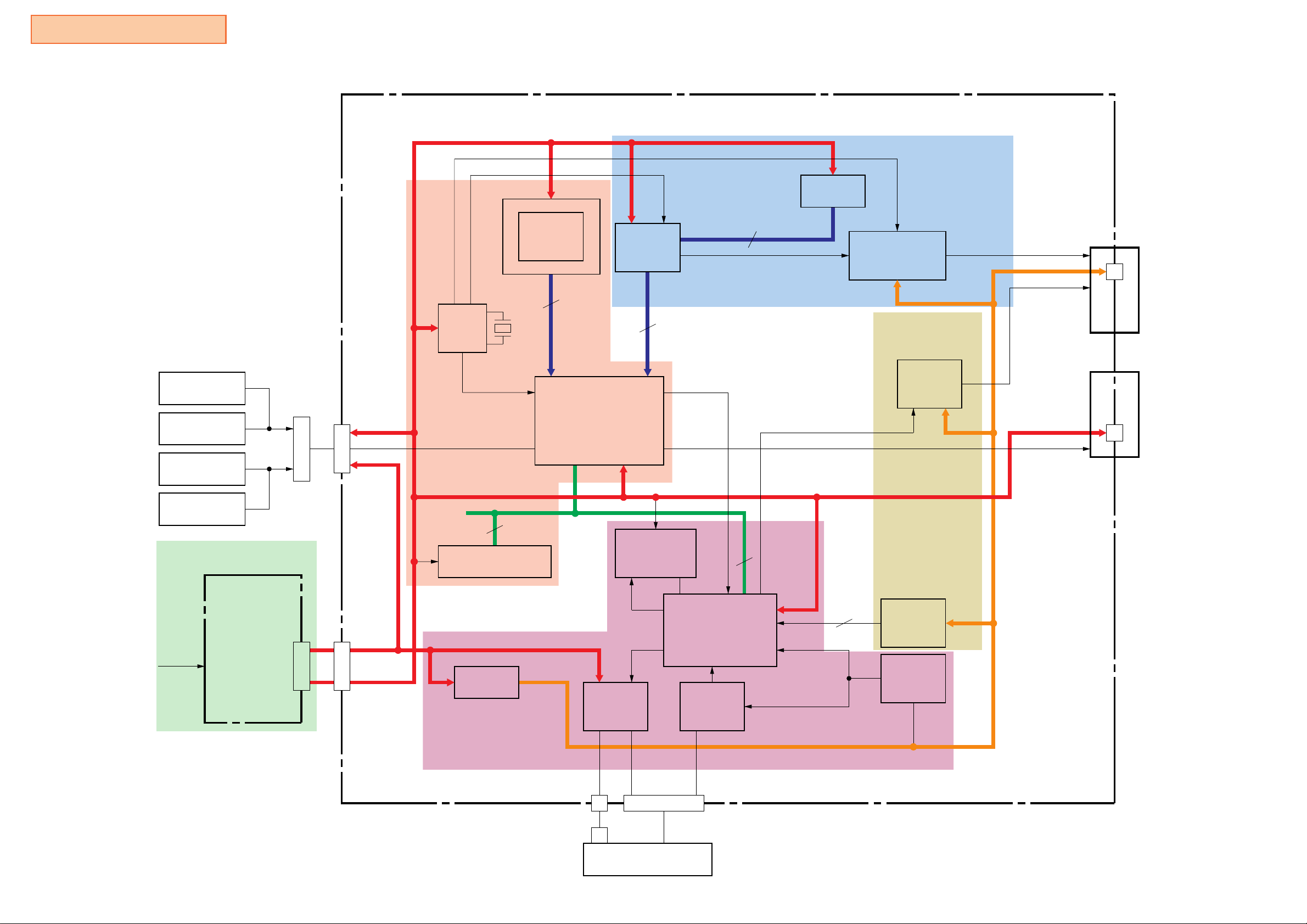
SECTION 5
BLOCK DIAGRAMS
NTSC : 53.693175MHz
PAL : 53.203425MHz
IC201
(SG-RAM)
SCPH-9000 SERIES
NTSC : 3.58MHz
PAL : 4.43MHz
MEMORY
CARD
CONTROLLER
CONTROLLER
MEMORY
CARD
POWER
TERMINAL
BOARD
FRONT
CN102
CTR3.3V
EXT +8V
IC204
67.7376MHz
CPU
8
IC102
(BOOT RAM)
IC106
(DRAM)
16Mbit
32
X201
IC103
(CPU)
CXD8606
SUB BUS
IC203
(GPU)
CXD8561
MAIN BUS
32
33.8688MHz
IC304
(SUB CPU)
MC68HC05G6
32
VIDEO
16
IC502
VDAC +RGB
(
ENCODER
VID +5V
IC405
(DAC)
NJM2174
AUDIO
)
AUD +5V
VIDEO OUT
AUDIO OUT
CN502
AV MULTI OUT
CN104
SERIAL I/O
AC IN
POWER
SUPPLY
BLOCK
+8V
+3.5V
CN602
+3.3V
MOT +8V
IC601
78M05
5V
SERVO
4.19MHz
IC732
(CD-ROM
CONTROLLER
+ CD DSP)
CXD2938
IC722
(DRIVER)
BA5977
CN701 CN702
OPTICAL DEVICE
KSM-440AEM
— 5 —
IC723
(CD, RF)
CXA2575
SER +3.3V
16
IC310
4Mbit
DRAM
IC602
(RIPPLE)
LP2985
Filter
DIG +5V
Page 7
Reproduction Prohibited
SCPH-9000 SERIES
CONTROLLER
SERIAL I/O
PU-23 BOARD
SCK0
102-10
TXD
102-8
RXD
102-6
DTR0A
102-5
DTR0B
102-3
DSR
102-2
INT
102-1
RXD
104-1
DSR
104-3
TXD
104-4
CTS
104-5
DTR
104-6
RTS
104-8
X201
REF.
OSC
14.318182MHz (NTSC)
17.37MHz (PAL)
+8V
+5V
REG.
FULL
F001
WAVE
RECT.
2A/125V
UC
1.6A/250V
AUS/UK/AEP
POWER SUPPLY BLOCK
IC204
PLL 1
PLL 2
PLL 3
+3.5V
REG.
DC-AC
CONV.
SWITCHING
REG.
Q106 (1/2)
Q106 (1/2)
Q105 (1/2)
Q105 (1/2)
EP ROM
CONFIGURABLE
MULTIPLEXER
AND
DIVIDE LOGIC
SER +3.5V
+5V
5 67MHz
53.63MHz (NTSC)
1
53.20MHz (PAL)
3.58MHz (NTSC)
6
4.43MHz (PAL)
RECT.
RECT.
81
83
84
80
77
82
89
75
73
74
71
72
70
43, 4
SCK0
TXD0
RXD0
DTR0A
DTR0B
DSR0
INTIN10
RXD1
DSR1
TXD
CTS1
DTR1
RTS1
CRYSTALP
RECT.
IC103
CPU
GTE
CPU CORE
SIO
MDEC
+8V
+3.5V
SYSTEM
RESET
B/U
DRAM
CONTROLLER
RES3.3
VD0-VD31
SD0-SD15
SA0-SA23
DD0-DD31
DA0-DA7
DA11
DWE
DRAS0
DCAS0-DCAS3
INT IN1
TCLK1
TCCK0
INT IN0
DREQ2
SYSCLK0
DACK2
VWR
DSYSCLK
DREQ4
INT IN9
DACK4
SWR0
SYSCLK1
INT IN2
161-165, 172-181, 184-194, 197, 198
MAIN DATA BUS (GPUD0-GPUD31)
107-116, 119-142
SUB DATA BUS (SD0-SD15)
145-152, 132-142, 125-129
ADDRESS BUS (SA0-SA23)
97
CS2
5-13, 16-25,
28-37, 40-42
55, 57, 59-64
67, 68
DA9
43
45
46-49
102
GPUNIT
153
VA2
VRD
CS7
CS4
SRD
CS5
GPUA2
159
H BLANK
160
PCK
199
V BLANK
200
GPUDREQ
201
SYSCLK0
202
GPUDACK
203
GPUWR
204
GPURD
205
GPUCS
206
DBLCLK
SPUDREQ
88
SPUNIT
90
SPUDACK
87
SPUCS
96
101
SRD
100
SWR0
154
SYSCLK1
95
94
2-5, 7-10,13-16,18-21
50-53,55-58,61-64,66-69
4
S301
19
DOOR
SRD
28-34, 37-39
IC304
SUB CPU
DECD0-DECD7
DECA0-DECA4
24
A0-A19 D0-D7
OE
22
CE
HYPER DRAM (16M)
I/O1-I/O32
A0-A9
44
WE
27
RAS
OE
49
LDON
28
MIRROR
27
SPEED
43
DATA
44
XLT
45
CLK
31
SCOR
26
SQCK
24
SUB Q
18
LMTSW
14
DSC1
13
RESET
46
DECCS
47
DECWR
48
DECRD
30
X INT
23
SENSE
23, 25-31
1-12
IC102
BOOT RAM
IC106
IC106
CAS1-4
45-48
SPUDREQ
SPUNIT
SPUDACK
SRD
SWR0
SPUCS
SYSCLK1
EXTDATA
33-38, 40, 41
6-10
LDON
AGC_CNT
SPEED
DAT0
XLT0
CLK0
SCOR
SQCK
SUB Q
LS
MCLK
XRST
MCS
MWR
MRD
MINT
SENS
CD RD CS
CD RD INT
36
35
34
32
33
31
41
96
13-15,
17-21
DREQ
XIRQ
DACK
XRD
XWR
XCS
SYSCLK1
DTIB
RES3.3
RES3.3
24-28, 31-36, 39-42,
45-50, 53-59, 62-65
GPUNIT
GPUA2
H BLANK
PCK
V BLANK
GPUDREQ
SYSCLK0
GPUDACK
GPUWR
GPURD
GPUCS
DBLCLK
1, 2, 5-14
16-19
SD0-SD15
20-27, 30
SA1-SA9
FROM IC103
125-142
SD0-SD15
105,107-111,113-116
SA0-SA9
MCD0-MCD7MCD0-MCD7
97-99,101,102
MCA0-MCA4MCA0-MCA4
6
RST
D0-D31
13
IREQ
2
A2
14
H BLANK
199
PCK
17
V BLANK
12
DREQ
9
SYSCLK
5
DACK
4
WR
3
RD
1
CS
206
D SYSCK
192
VCKN-A
FD0-FD31 LA0-LA9
77-79, 82-86
89-95, 98-104
107-112, 115-118
1, 3, 4, 6, 7, 9, 10,
12, 13, 17, 18, 20,
21, 60, 61, 63, 64,
68, 69, 71, 72, 74,
75, 77, 78, 80, 81,
83, 84
DQ0-DQ31 A0-A9
SPUDREQ
SRD
SWR0
SPUDACK
SYSCLK1
HD0-HD15
HOST
HA1-HA8
DTIB
BCK0
LRC0
HD0-HD15
HA0-HA9
85-92
SUB CPU
I/F
74
DATA
75
XLAT
76
CLOK
77
SCOR
80
SQCK
81
SQS0
11
FSOF
94
XCS
95
XWR
96
XRD
79
XINT
82
SENS
103
XHCS
117
H INT
IF
IC203
GPU
DQMH
DQMLWECAS
RAS
MCS0
DSF
126
8x
8x
125
WE
124
122
CAS
RAS
GENERATOR
MCLKOUT
123
131
55
CS
CLK
DSF
∆
∑
MOD
∆
∑
MOD
PWM
GENERATOR
TIMING
SERIAL
SG RAM
DMA
IF
137-140
143-145
148-150
29, 31-34
47-51
TIMING
GEN
SERIAL
INPUT
INTERFACE
SERVO DSP
127
128
565723242526272853
DQM1
DQM3
DQM0
DQM2
ENV
DSP
INTERPOLATOR
INTERPOLATOR
A/D
CONVERTER
MIRR
DFCT
FOK
SYNC
PROTECTOR
CD-ROM CONTROLLER + CD DSP
SR0-SR7
SG0-SG7
SB0-SB7
C SYNC
NTPL
MCLKIN
134
IC201
EXRAM
SWITCH
BUFFER
IF
SCF
SCF
AND
TRACKING
GENERATOR
TRACKING
GENERATOR
TRACKING
GENERATOR
PROTECTOR
156
157
MD0-MD15
MA1-MA9
PWM
PWM
PWM
CLV
R
G
XOE
XWE
XRAS
XCAS
MUTO
AOUTL
AOUTR
XLT1
XHRD
XHWR
SYSCK
IC732
DECODER
DECODER
DECODER
14
SYNC IN
15
SC IN
13
NT/PAL
160-164, 166-172
174-177
183-186, 188-192
181
179
182
178
154
147
150
105
27
37
38
39
57
55
53
54
58
59
122
119
120
144
R
G
B
MED0-MED15
MEA0-MEA8
RFAC
FE
SE
TFDR
TRDR
FRDR
FFDR
SRDR
SFDR
SRD
SWR0
SYSCLK1
LATCH
LATCH
LATCH
FROM IC103
VIDEO DAC + RGB ENCODER
CELL
MATRIX
CELL
MATRIX
CELL
MATRIX
SPMUTE
AU-R
AU-L
RESET
SPMUTE
2-5, 7-10
31-34, 36-39
16-19, 22-26
27
13
14
28
29
CLAMP
CLAMP
CLAMPB
5
7
11
INTERPOLATOR
INTERPOLATOR
4
5
IC310
I/O 1-16
A0-A8
4Mbit DRAM
OE
WE
RAS
UCAS
LCAS
6
7
5
4
22
23
2
3
SPEED
20
RESET
IC502
MATRIX
BURST
FLAG
SERIAL INPUT
INTERFACE
8x
8x
SPCLK
AMP
AMP
AMP
AMP
R
G
B
Y
B-Y
R-Y
CLOCK DIVIDER
6 7
IC722
DRIVER
LEVEL
SHIFT
LEVEL
SHIFT
LEVEL
SHIFT
LEVEL
SHIFT
SYNC
ADD
CHROMA
GEN.
IC405
∆
∑
MODULATOR
∆
∑
MODULATOR
15
13
11
12
16
BUFF
BUFF
BUFF
BUFF
BUFF
BUFF
BUFF
BUFF
6dB 75
6dB 75
6dB 75
6dB 75
LPF
BPF Y TRAP
Y/C
M/X
SCF
SCF
19 18
VREFL
+5V
IC723
CD-RF
AMP
AMP
APC
9
11
12
13
14
17
18
15
16
M_R
502-2
M_G
502-1
M_B
502-4
M_Y
502-8
M_C
M_VIDEO
Q701
REG
M_AUL
M_AUR
502-6
502-7
AV MULTI OUT
502-11
502-9
KSM440AEM
702-7
702-6
702-8
702-4
702-9
702-1
702-10
702-15
702-14
702-16
702-13
701-1
701-2
701-4
701-3
LD
702-12
PD1
PD2
PDIC
E
F
LASER DIODE
MI
LD
TRK–
TRACKING
COIL
TRK+
FCS–
FOCUS
COIL
FCS+
SL–
SLED
M
MOTOR
SL+
SP–
SPINDLE
MOTOR
SP+
BLOCK
75
75
VOOM
12
TRM_L
13
TRM_R
2
7
AMP
6
AMP
5
AMP
4
AMP
8
+B
— 6 —
Page 8
Reproduction Prohibited
THIS NOTE IS COMMON FOR PRINTED WIRING
BOARDS AND SCHEMATIC DIAGRAMS.
Note on Printed Wiring Boards :
••Through hole is omitted.
: Pattern on the side which is seen.
SCPH-9000 SERIES
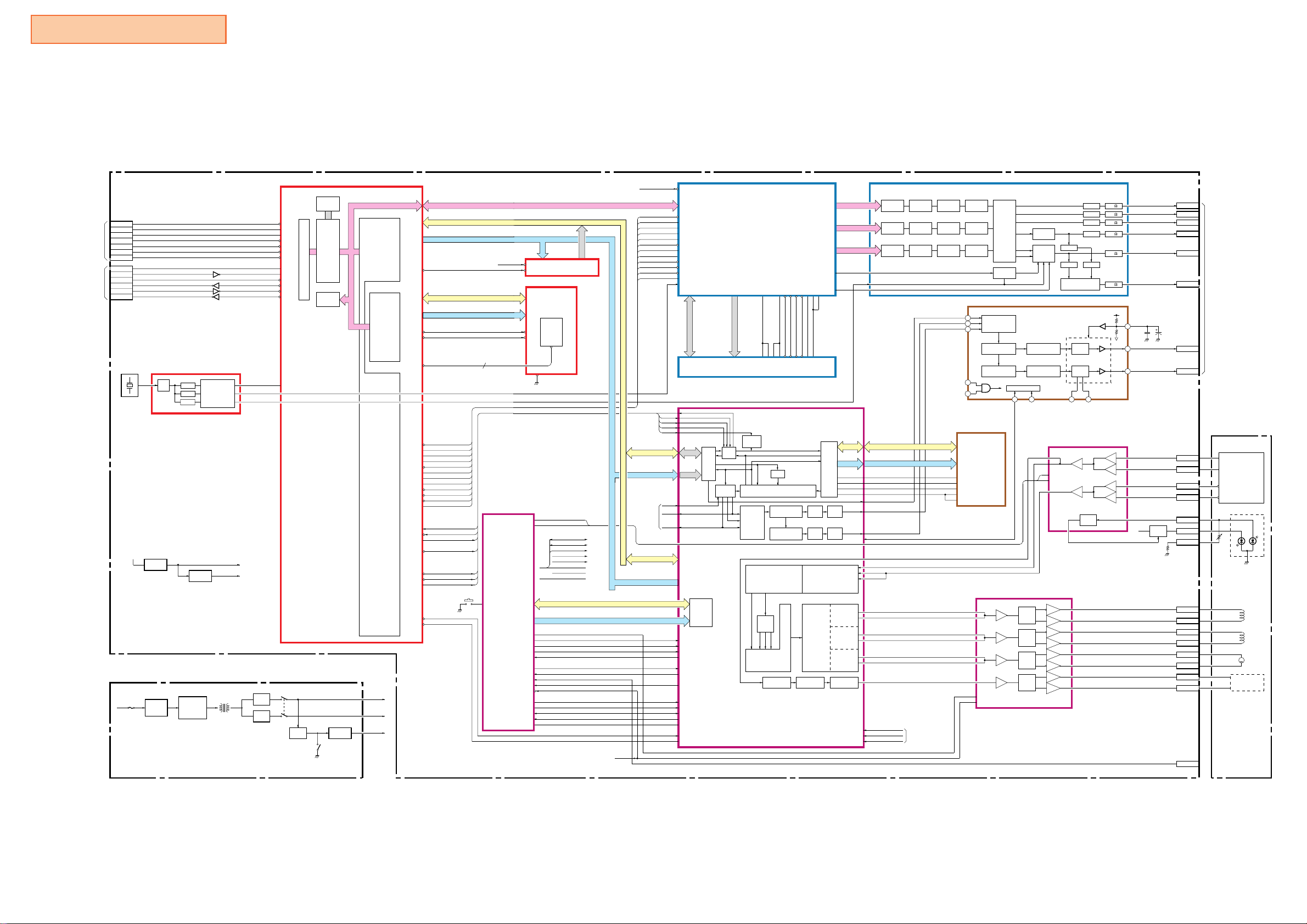
SECTION 6
PRINTED WIRING BOARDS AND SCHEMATIC DIAGRAMS
Note on Schematic Diagram :
•
Use caution when replacing chip parts.
New parts must be attached after removal of chip.
Be careful not to heat the minus side of tantalum capacitor,
because it is damaged by the heat.
•
All capacitors are in µF unless otherwise noted. pF : µµF 50 WV
or less are not indicated except for electrolytics and tantalums.
•
All resistors are in and 1/4 W (Chip resisters : 1/10w) unless
otherwise specified.
•
Chip resistors are 1/8 W or 1/10 W unless otherwise noted.
k : 1000 , M : 1000 k .
Note :
The components
identified by mark
dotted line with mark
are critical for safety.
Replace only with part
number specified.
!
or
Note :
Les composants identifies par
une marque ! sont critiques
!
pour la securite.
Ne les remplacer que par une
piece portant le nubero specifie.
— 7 —
Page 9

Reproduction Prohibited
8 97
1-674-987- 41
IC310
IC602
35
36
13
45
52
1
1
28
1
156
157
20
21
40
208
104
1
32
105
1357
2468
C118
C122
C641
C611
C137
C108
C109
RB123
RB119
ET101
R154
C702
R619
RB122
S301
C129
C130
L606
FB602
C617
C317
C637
C705
C745
R706
R704
R705
C703
C706
C776
FB111
FB114
FB112
CL607
CL134
CL136
CL103
CL104
CL138
CL102
CL166
CL705
CL133
CL167
CL111
CL526
CN104
FB115
FB113
FB116
CL527
CL528
CL529
CL530 CL532
CL531
CL160
CL115
C102
C151
C140
CL120
CL124
CL126
CL161
CL143
CL154
CL159
CL149
CL127
CL125
CL158
L102
CL533
CL164
CL614
CL795
CL762
C768
CL794
CL793
CL774
CL792
CL796
CL761
CL799
CL610
L607
C731
R702
R703
R701
R725
C704
C733
C724
C327
C315
C132
C131
C133
C315
C775
C767
C124
C139
C101
RB120
RB124
R134
R135
R338
Q106
Q105
R136
R148
R146
D104
RB121
4
7
R54
C530
R430 R426
L
C
R
R
C
C
7
C725
PU-23 BOARD (-11/-21/-31/-41/-51)
C5
C511
C510
48
IC502
13 2
3
C502
R528
3
L604
C608
C609
CL608
CL509
R543
R501R502
C508
1
12
C523
C424
C423
C409
C404
C406
C408
R423
C
C509
C407
14 8
IC405
34
17
47
Suffix of -51 Suffix of -51
L401
SCPH-9000 SERIES
A
B
C
D
E
F
CL526
L102
CL533
R901 R903R902
RB120
C118
2468
CN104
1357
FB113
CL527
FB115
CL528
FB116
R146
R148
R136
R904
CL164
C139
105
104
CL103
CL136
C133
52
C132
36
35
C122
CL607
C108
C109
L606
FB111
RB122
RB123
CL104
RB124
C101
C137
D104
CL138
C131
C129
CL134
CL529
CL531
S301
1
C130
20
C611
FB602
45
IC602
CL530
Q106
R135
R134
C316
CL532
FB114
FB112
RB119
IC310
C317
C641
13
C327C315
CL614
C617
CL610
Q105
CL102
L607
R154
C124
C637
ET101
CL166
R619
CL705
CL133
CL167
40
C702
CL795
C768
CL794
CL762
CL793
21
CL125 CL122 CL157 CL123
CL127
CL124
CL120
CL154
CL159
CL126
C151
C102
CL160
CL115
CL158 CL156 CL130 CL109
C140
CL149
CL161
116
CL143
R338
C767
C775
IC102
CL121
CL110
C773
CL144
157
CL145
CL112
CL146
CL147
CL142 CL141
CL108
CL155
CL113
1732
CL107
CL114
CL106
CL140
C744
CL315
C150
R345 R344
105156
104
L304
C319
14
IC304
26
27 39
C326
R795
C774
C743
C736
C306
113
52
40
R740
IC723
1
C763
C762
IC732
CL773
CL769
R783
2
1
C701
C741
CL727
FB701
FB704
53
C725
CL784
CL791
R793
CL785
C726
CL790
C761
CL709
R770
CN701
CL787
R775
CL711
C720
14
208
152
CL774
CL796
CL792
C731
C705
C776
CL799
CL761
R712
C714
C709
C715
R710
IC722
114
R725
C724
C733
C704
R701
R703
R702
C703
C706
R705
C745
R704
CL719
R706
R714
R774
C747
C749
CL760
R717
CL704
1528
R723
C729
FB702
R748
R749
R769
C740
610 16
CN702
59
CL777
CL776
CL775
CL779
CL710
Q701
R732
R733
C739
R727
CL786
FB703
7 8 9 10 11 12
Note : PU-23 board number suffix of -41 is described partially.
R775
CL727
CL607
L606
C641
FB602
45
IC602
CL614
C617
C618
13
C637
CL610
L607
15
14
— 8 —
FB701
CL784
CL785
C718
CN701
CL787
R727
14
CL
FB703
C325
R342
R341
R341
R734
R739
R738
R741
1120
R796
C728
C737
10
R746
CL316
L701
FB710
13
CL780CL778
CL728
HA002
R747
15
CL706
C738
CL708
R750
CL783
C742
CL782
CL781
R745
1-674-987- 31
11
21
2
CN502
1
C524
C635
CL604
C602
PS604
C627
5
1
CL612
C621
123456
C631
C622
R606
CN602
C606
PS605
CL603
CL503
CL608
L604
C608
C609
C642
IC601
1
C607
PS603
C620
CL502
CL509
D510
CL501
R519
2
C639
R139
R150
CL137
C639
R150
CL137
R517
R518
R521
R520
PS601
FB123
FB123
D511
R522
D103
3
CL611
CL152
L106
FB121
R140
L106
CL504
1
D103
R140
FB504
CL505
2
CL131
CL199
FB122
CL199
C508
12
CL116
R142
1
L507
PS602
FB119
R141
CL116
FB502
CL508
C510
C523
CN102
CL119
CL105
CL105
12
11
FB503
D503
C519
C511
C502
IC502
13 24
R501
C523
C601
L104
CL605
10
9
CL150
FB120
FB117
FB118
R132
D101
R138
R137
CL150
FB120
FB117
FB118
R132
D101
R138
R137
CL512
FB401
CL510
FB402
C227
C211
C220
IC201
C243
C224 C226
C225
C244
IC203
C210
C210
X201
X201
C221
C236
C209
1
4
C209
1
4
C241
R205
CL201
R620
R206
IC204
R205
CL201
R620
R206
IC204
C222
1
100
81
80
C219
8
5
R204
C219
8
5
R204
C551
R528
R542
CL613
C509
3748
Q505
R527
CL507
R541
R529
C550
CL506
30
31
C228
50
51
R215
36
C208
25
C239
105
C245
FB201 FB202
C216
CL118
C248
CL606
CL151
C214
C249
ET102
156
C240
157
CL205
CL206
R133
R133
C605
L601
CL601
Suffix of -51 Suffix of -51 Suffix of -51 Suffix of -51
C530
R430 R426
C409
C424
C407
14 8
C404
IC405
C423
R425 R429
CL162
1
CL128
R107
C113
CL163
CL117
C408
C529
C406
C145
C114
C104
C111
IC103
C106
IC106
C146
C134
R104
C110
CL111
RB121
C223
CL534
C247
C242
CL101
CL511
L401
C445
CL132
C138
17
CL401
CL129
FB102
156
157
53104
C218
52
C144
C112
C215 C217
C105
C213
R207
208
R115
C136
C238
1
70
RB125
208
JR201
L203
C234
C235
JR202
1
JR203
C116
C115
208
JR201
L203
C234
C235
JR202
JR203
Page 10

Reproduction Prohibited
PU-23 (1/4)
VBLANK
IC203 17 pin
GPUDREQ
IC203 12 pin
SYSCLK0
IC203 9 pin
GPUDACK
IC203 5 pin
GPUWR
IC203 4 pin
GPURD
IC203 3 pin
GPUCS
IC203 1 pin
IC203 206 pin
DBLCLK
DIG_+3.3V
DIG GND
CPUCLK
IC204 5 pin
IC203 65 pin GPUD0
IC203 64 pin
GPUD1
IC203 63 pin
GPUD2
IC203 62 pin
GPUD3
IC203 59 pin
GPUD4
IC203 58 pin
GPUD5
IC203 57 pin
GPUD6
IC203 56 pin
GPUD7
IC203 55 pin
GPUD8
IC203 54 pin
GPUD9
IC203 53 pin
GPUD10
IC203 50 pin
GPUD11
IC203 49 pin
GPUD12
IC203 48 pin
GPUD13
GPUD14
IC203 47 pin
IC203 46 pin
GPUD15
IC203 45 pin
GPUD16
IC203 42 pin
GPUD17
IC203 41 pin
GPUD18
IC203 40 pin
GPUD19
IC203 39 pin
GPUD20
IC203 36 pin
GPUD21
IC203 35 pin
GPUD22
IC203 34 pin
GPUD23
IC203 33 pin
GPUD24
GPUD25
IC203 32 pin
IC203 31 pin
GPUD26
IC203 28 pin
GPUD27
IC203 27 pin
GPUD28
IC203 26 pin
GPUD29
IC203 25 pin
GPUD30
IC203 24 pin
GPUD31
RES3. 3G
EXT_+8V
DIG_+3.3V
CTR_3.3V
DIG GND
DIG_+3.3V
CL105
CL199
CL150
CL116
CL119
ET101
GPUD0
GPUD1
GPUD2
GPUD3
GPUD4
GPUD5
GPUD6
GPUD7
GPUD8
GPUD9
GPUD10
GPUD11
GPUD12
GPUD13
GPUD14
GPUD15
GPUD16
GPUD17
GPUD18
GPUD19
GPUD20
GPUD21
GPUD22
GPUD23
GPUD24
GPUD25
GPUD26
GPUD27
GPUD28
GPUD29
GPUD30
GPUD31
ET102
FB120
CL117
GPUD0
GPUD1
GPUD2
GPUD3
GPUD4
GPUD5
GPUD6
GPUD7
GPUD8
GPUD9
GPUD10
GPUD11
GPUD12
GPUD13
GPUD14
GPUD15
CPMA0
CPMA1
CPMA2
CPMA3
CPMA4
CPMA5
CPMA6
0.6 (1.4)
0.6 (1.4)
0.8 (1.4)
0.8 (1.3)
0.9 (1.2)
0.9 (1.2)
0.8 (1.3)
0.8 (1.1)
1 (1.6)
0.8 (1.1)
0.9 (1.2)
0.8 (1.1)
0.6 (1)
0.8 (1.4)
0.6 (0.8)
2.6 (1.9)
3.1 (1)
2.7 (1)
0.7 (2)
2.7 (1.9)
2.4 (1)
2.5 (1)
3.1 (1)
CN102 10P
CN104 8P
SIO_+3.3V
3.4
3.4
3.4
3.4
1
3.4
SCK0
+3.3V
GND
DTR0A
DTR0B
SIO_GND
TXD
RXD
+8V
DSR
INT
RXD
DSR
TXD
CTS
DTR
RTS
C115
0.01u
B
C116
100p
C113
0.1u
F
IC106
T7X16 (YEL)
VCC
I/O1
I/O2
I/O3
I/O4
VCC
I/O5
I/O6
I/O7
I/O8
N. C.
VCC
I/O9
I/O10
I/O11
I/O12
VCC
I/O13
I/O14
I/O15
I/O16
N. C.
N. C.
N. C.
N. C.
N. C.
RAS
A0
A1
A2
A3
A4
A5
A6
35 34 33 32 31 30 29 28 27 26 25 24 23 22 21 20 19 18 17 16 15 14 13 12 11 10 9 8 7 6 5 4 3 2 1
VCC
CAS1
CAS2
CAS3
CAS4
I/O32
I/O31
I/O30
I/O20
I/O28
I/O27
I/O26
I/O25
N. C.
I/O24
I/O23
I/O22
I/O21
I/O20
I/O19
I/O18
I/O17
N. C.
N. C.
N. C.
N. C.
VSS
VSS
VSS
VSS
WE
DE
A9R
A8
A7
VSS
IC106
DRAM
C114
0.001u
B
C146
0.001u
B
C118
0.001u
B
C122
0.001u
B
Suffix of -11/-21/-31/-41Suffix of -51
CL105
10
CL199
9
CL116
8
7
CL119
6
CL150
5
4
CL131
3
2
CL152
1
CL527
1
CL526
2
CL529
3
CL528
4
CL531
5
CL530
6
CL533
7
CL532
8
1.9 (1.4)
9.2 (1.1)
2 (1.1)
0.2 (1.3)
0.3 (1)
0.3 (1.4)
0.3 (1.5)
0.2 (1.5)
0.2 (1.2)
0.2 (1.2)
0.3 (1.2)
0.2 (1.2)
0.3 (1.2)
0.3 (1.4)
0.3 (1.3)
0 (1.5)
3.2 (3)
3.2 (3)
3.2 (3)
3.2 (3)
3
0 (0.8)
1.8
0.3 (1.9)
36 37 38 39 40 41 42 43 44 45 46 47 48 49 50 51 52 53 54 55 56 57 58 59 60 61 62 63 64 65 66 67 68 69 70
FB122
FB121
FB120
FB119
FB118
FB117
FB123
D103
MAZ9120D0LS0-JX/L
CL151
GPUD31
GPUD30
GPUD29
GPUD28
GPUD27
GPUD26
GPUD25
GPUD24
GPUD23
GPUD22
GPUD21
GPUD20
GPUD19
GPUD18
GPUD17
GPUD16
CPMA9
CPMA8
CPMA7
FB115
FB113
FB116
FB111
FB114
FB112
FB124
SCPH-9000 SERIES
IC203 199 pin
PCK
IC203 14 pin
HBLANK
IC203 2 pin
GPUA2
IC732 144 pin
SYSCLK1
SA0
IC102
MSM534031E-07GS-KPR2
0 3.4
AEP
169459221
141481321
141481321
141481321
141481321
141481321
141481321
875953754
SA19
A19
00
SA16
A16
00
SA15
A15
3.4 0
SA12
A12
00
SA7
A7
00
SA6
A6
00
SA5
A5
0 3.4
SA4
A4
0 3.4
SA3
A3
00
SA2
A2
0 3.4
SA1
A1
0 3.4
SA0
A0
3.4 3.4
SD0
D0
3.4 3.4
SD1
D1
3.4 3.4
SD2
D2
VSS
16 15 14 13 12 11 10 9 8 7 6 5 4 3 2 1
E32
169459221
141481321
141481321
141481321
141481321
141481321
141481321
875953749
CL102
C150
0.01u
12
13
C102
0.001u
C140
0.01u
C151
0.01u
VCC
A18
A17
A14
A13
A11
A10
B
SA18
SA17
SA14
SA13
SA8
A8
SA9
A9
SA11
OE
SA10
CE
D7
D6
D5
D4
D3
SA7
SA6
SA5
SA4
3.4
SA3
17 18 19 20 21 22 23 24 25 26 27 28 29 30 31 32
RB125
C133
22
0.001u
B
C105
0.001u
B
C134
0.001u
B
C104
0.001u
3.4
B
3.4
1.7
1.9 (1.4)
CPMD31
0.2 (1.1)
CPMD30
CPMD29
CPMD28
CPMD27
CPMD26
CPMD25
CPMD24
CPMD23
CPMD22
CPMD21
CPMD20
CPMD19
CPMD18
CPMD17
CPMD16
CPMD15
CPMD14
CPMD13
C106
0.001u
CPMD12
CPMD11
CPMD10
CPMD9
CPMD8
CPMD7
CPMD6
CPMD5
CPMD4
CPMD3
CPMD2
CPMD1
CPMD0
RB121
22
RB120
22
D101
D104
2 (1.3)
0.2 (1.3)
0.3 (1)
0.3 (1.4)
0.3 (1.5)
0.2 (1.5)
0.2 (1.2)
3.4
0.2 (1.2)
0.3 (1.2)
0.2 (1.2)
0.3 (1.2)
0.3 (1.4)
0.3 (1.3)
0 (1.5)
0.6 (0.8)
0.8 (1.4)
0.6 (1)
C132
0.001u
L102 1uH
3.4
1
0.8 (1.1)
0.9 (1.2)
0.8 (1.1)
1 (1.6)
0.8 (1.1)
0.8 (1.3)
0.9 (1.2)
0.9 (1.4)
0.8 (1.3)
3.4
0.8 (1.4)
2.7 (1.3)
0.6 (1.4)
3.4 (2.6)
2.6 (1.9)
3.4
3.2 (3)
3.2 (3)
3.2 (3)
3.4
B
L106 1uH
L104 1uH
C152
0.01u
B
B
208 207 206 205204 203 202 201 200 199 198 197196 195 194 193 192 191 190189188 187 186 76 184 183 182 181 180179 178 177 176 175 174 173 172171 170 169 168 167 166 165164163 162 161 160 159 158 157
VSS
VDD
VDD
CRYSTALN
CRYSTALP
DD31
DD30
2
DD29
DD28
DD27
DD26
DD25
DD24
DD23
VDD
VSS
DD22
DD21
DD20
DD19
DD18
DD17
DD16
DD15
DD14
DD13
VDD
VSS
DD12
DD11
DD10
DD9
DD8
DD7
DD6
DD5
DD4
DD3
VDD
VSS
DD2
DD1
DD0
DWE
DRAS1
DRAS0
DCAS3
DCAS2
DCAS1
DCAS0
VDD
VSS
VSS
52 51 50 49 48 47 46 45 44 43 42 41 40 39 38 37 36 35 34 33 32 31 30 29 28 27 26 25 24 23 22 21 20 19 18 17 16 15 14 13 12 11 10 9 8 7 6 5 4 3 2 1
VDD
53 54 55 56 57 58 59 60 61 62 63 64 65 66 67 68 69 70 71 72 73 74 75 76 77 78 79 80 81 82 83 84 85 86 87 88 89 90 91 92 93 94 95 96 97 98 99 100 101 102103 104
3.4
3.4
B
C136
0.001u
R146
1.6
VSS
1
VDD
1.8
CPMA8
1k
3.2
3.4 (3.2)
CS7
DSYSCLK
3 4
DA11
DA10
CL118
R148
1k
3.1
VRD
DA9
0 (0.8)
CPMA9
R134
1k
00
22
GPUD31
GPUD30
R115
3.4 (3.2)01.6
1.3 (3.1)
0.3
3.3
3.4 (3.1)
VSR
VD31
VD30
INTIN0
DACK2
DREQ2
SYSCLK0
6
5 7
DA8
DA7
DA6
DA5
DA4
DA3
DA2
0.3 (1.9)
3.1 (1)
2.5 (1)
2.4 (1)
2.7 (1.9)
0.7 (2)
CPMA7
CPMA6
CPMA5
CPMA4
CPMA3
CPMA2
R133
R132
1k
1k
Suffix of -11/-21/-31/-41
R135
R136
470
470
RB119
22
3.2
Q106
3.4
3.4
VDD
VSS
3.4
Q105
GPUD29
GPUD28
3.3
3.3
VSS
VD29
VDD
DA1
2.7 (1)
3.1 (1)
CPMA1
CPMA0
00
GPUD27
GPUD26
3.3
3.3
VD28
VD27
VD26
DA0
RC_NET
RTS1
3.4
3.403.403.4
GPUD25
GPUD24
GPUD23
GPUD22
3.3
3.3
0 (3.2)
0 (3.2)
VD25
VD24
VD23
IC103
CTS1
OTA1
OSA1
3.4
GPUD21
3.3
VD22
TXD1
3.4
GPUD20
3.3 (3.1)
VD21
RXD1
3.4
C129
100p
GPUD19
C112
0.1u
F
3.4 (3.1)
3.4
VDD
VD20
VD19
CPU
IC103
CXD8606Q
EXT_RESET
DTA0B
VSS
3.4
C108
0.001u
R141
470
R140
470
R139
470
R138
470
R142
470
R137
47
R150
47
C130
100p
GPUD18
GPUD17
GPUD16
GPUD15
GPUD14
GPUD13
GPUD12
GPUD11
GPUD10
GPUD9
GPUD8
GPUD7
GPUD6
GPUD5
GPUD4
GPUD3
GPUD2
GPUD1
GPUD0
C144
0.001u
B
3.4 (3.2)
3.4 (3.2)
3.4 (3.2)
3.4 (3.2)
3.4 (3.2)
3.4 (3.2)
3.4 (3.2)
3.4 (3.2)
3.4 (3.2)
3.4 (3.2)
3.4
3.4 (3.2)
3.4 (3.2)
3.4 (3.2)
3.4 (3.2)
3.4 (3.2)
3.4 (3.2)
3.4 (3.2)
3.4 (3.2)
3.4
1.7
0.8
3.4
3.4
VD9
VD6
VD7
VD6
VD5
VD4
VD3
VD2
VD1
VSS
VD18
VD17
VD16
VD15
VD14
VD13
VDD
DTR0A
SCKO
DSAO
TXD.0
RXD.0
DACK5
3.4
B
000
3.4
3.4
3.4
3.4
3.4
CL136
C101
100p
CH
VD12
DREQ5
VD11
DACK4
0
VD10
DREQ4
2.6
INTIN10
3.4
C131
100p
VDD
INTIN9
VSS
VSS
3.4
C124
R154
330
VDD
CSHTST
INTIN2
3.4
3.4 (3.2)
1u
Suffix of -51
R138
470
R137
R150
VD0
VDD
VDD
TCLK0
TCLK1
89
CS5
CS4
CS2
CS0
SWR1
3.4
3.4
3.4
3.4
CL138
47
47
SYSCLK1
10
11
SWR0
SRD
INTIN1
VSS
VSS
3.4
3.4
3.4
RB126
470
SA23
SA22
SA21
SA20
SA19
SA18
SA17
SA16
SA15
SA14
SA13
SA12
SA11
SA10
SD15
SD14
SD13
SD12
SD11
SD10
C145
0.001u
B
C111
0.001u
B
VSS
VSS
1.6
2.1 (1.2)
VA2
3.4
CL163
0
CL129
0
CL162
0
CL128
0
CL161
0
CL127
0
CL160
0
CL126
3.4
VDD
VSS
141 142 143 144145 146 147 148 149 150 151 152153 154 155 156125 126 127 128129 130 131 132 133 134 135 136137 138 139 140109 110 111 112 113 114105 106 107 108 115 11 6 117 118 119 120 121 122 123 124
SA9
SA8
SA7
SA6
SA5
VDD
VSS
SA4
SA3
SA2
SA1
SA0
VDD
VSS
SD9
SD8
SD7
SD6
SD5
SD4
SD3
SD2
SD1
SD0
VDD
VDD
CL104
CL103
CL137
CL159
0
0
CL125
0
CL158
CL124
3.4
CL157
3.4
0
CL123
CL156
0
CL122
0
0
CL155
CL121
0
0
CL154
0
CL120
0
CL149
0
CL115
0
CL148
0
CL114
0
3.4
R104
3.4
3.4
3.4
3.4
3.4
3.4
CL134
3.4
CL144
3.4
CL110
3.4
CL143
3.4
CL109
3.4
CL142
3.4
CL108
3.4
CL141
3.4
CL107
3.4
CL140
3.4
CL106
3.4
C137
0.001u
3.4
C138
0.01u
C139
0.01u
C109
0.001u
B
C110
0.001u
22
CL101
RB124
22
SA23
SA22
SA21
SA20
SA19
SA18
SA17
SA16
SA15
SA14
SA13
SA12
SA11
SA10
SA9
SA8
SA7
SA6
SA5
B
SA4
SA3
SA2
SA1
SA0
SD15
CL147
SD14
CL113
SD13
CL146
SD12
CL112
SD11
CL145
SD10
CL111
SD9
SD8
SD7
SD6
SD5
SD4
SD3
SD2
SD1
SD0
10k
RB122
22
RB123
100
04. 29 1999.
ET102
FB111
FB112
FB113
FB114
FB115
FB116
IC102
FB102R107
J1
XX
121629591
121629591
121629591
121629591
121629591
121629591
875949657
IC102
BOOT ROM
USA
169459221
141481321
141481321
141481321
141481321
141481321
141481321
875953749
SA1
SA2
SA3
SA4
SA5
SA6
SA7
SA8
SA9
SD0
SD1
SD2
SD3
SD4
SD5
SD6
SD7
SD8
SD9
SD10
SD11
SD12
SD13
SD14
SD15
GPUINT
SRD
SWR0
SPUCS
CDADCS
CDRDINT
RES3.3
SPUINT
SPUDREQ
SPUDACK
— 9 —
SA0
SA1
SA2
SA3
SA4
SA5
SA6
SA7
SA8
SA9
SD0
SD1
SD2
SD3
SD4
SD5
SD6
SD7
SD8
SD9
SD10
SD11
SD12
SD13
SD14
SD15
IC203 13 pin
IC732 119 pin
IC732 120 pin
IC732 104 pin
IC732 103 pin
IC732 117 pin
IC732 118 pin
IC732 124 pin
IC732 121 pin
IC732 105 pin
IC732 107 pin
IC732 108 pin
IC732 109 pin
IC732 110 pin
IC732 111 pin
IC732 113 pin
IC732 114 pin
IC732 115 pin
IC732 116 pin
IC732 142 pin
IC732 141 pin
IC732 140 pin
IC732 139 pin
IC732 138 pin
IC732 136 pin
IC732 135 pin
IC732 134 pin
IC732 133 pin
IC732 132 pin
IC732 130 pin
IC732 129 pin
IC732 128 pin
IC732 127 pin
IC732 126 pin
IC732 125 pin
Page 11

Reproduction Prohibited
PU-23 (2/4)
SCPH-9000 SERIES
LA0
LA1
LA2
LA3
LA4
LA5
LA6
LA7
LA8
LA9
FD0
FD1
FD2
FD3
FD4
FD5
FD6
FD7
FD8
FD9
FD28
FD27
FD26
FD25
FD24
FD23
FD22
FD21
FD20
FD19
FD18
FD17
FD16
LA8
IC502 14 pin
IC502 13 pin
IC502 40 pin
IC502 39 pin
IC502 38 pin
IC502 37 pin
IC502 36 pin
IC502 35 pin
IC502 34 pin
IC502 33 pin
IC502 32 pin
IC502 31 pin
IC502 30 pin
IC502 29 pin
IC502 28 pin
IC502 27 pin
IC502 26 pin
IC502 25 pin
IC502 24 pin
IC502 23 pin
IC502 22 pin
IC502 21 pin
IC502 19 pin
IC502 18 pin
IC502 17 pin
IC502 16 pin
IC103 4 pin
IC502 15 pin
IC103 160 pin
IC103 206 pin
IC103 205 pin
IC103 153 pin
IC103 204 pin
IC103 203 pin
IC103 202 pin
IC103 201 pin
IC103 200 pin
IC103 102 pin
IC103 159 pin
IC103 199 pin
CSYNC
NTPL
DIG_+303V
DIG GND
CPUCLK
DBLCLK
GPUCS
GPUA2
GPURD
GPUWR
GPUDACK
RES3.3G
SYSCLK0
GPUDREQ
GPUINT
HBLANK
VBLANK
2.8 (3)
2.8 (3)
2.6 (3)
IC201
SGRAM
UPD481850GF-A12
1.8 (3)
2.7 (3)
2.6 (3.1)
FD8
FD9
FD15
FD14
1999. 02. 25 09 : 07
IC204
X201
C225
C226
0.1u
0.1u
F
F
R215
2.8 (3.1)
2.8 (3)
FD11
2.8 (3.2)
2.8 (3)
C227
0.1u
FD10
3.4
33
3.4
F
4.7k
2.6 (2.9)
34
31 32
3.3
2.6 (2.9)
2.6 (2.9)
USA
CY2081SL-500T
875949622
14.318182M
176778321
1.7
3.3
3.4
0
3.3
3.2 (3.4)
2.1 (3.1)
1.7 (1.2)
LA9
SEP
CY2081SL509T
875949623
17.73MHz
176794021
1.6
5049484746454443424140393837363534333231
1.7
1.3 (1.6)
1.8
3.4
1.7
1.7
1.7
1.5 (1.8)
E32
CY2081SL-500T
875949622
14.318182M
176778321
LA7
LA6
LA5
LA4
C228
0.1u
F
LA3
LA2
LA1
LA0
2.7 (3)
2.8 (3)
3.4
3.4
IC201
3.4
3.4
3.1
2.8 (3)
C224
0.1u
FD13
FD12
F
J1
CY2081SL-500T
875949622
14.318182M
176778321
C216
C214
C249
0.1u
0.001u
F
B
SB0
SB1
SB2
SB3
SB4
SB5
SB6
SB7
SG0
SG1
SG2
SG3
SG4
SG5
SG6
SG7
SR0
SR1
SR2
SR3
SR4
SR5
SR6
SR7
C235
0.001u
B
1.7
C234
0.1u
1.6
F
L203
82nH
1.6
X201
14.318182MHz (NTSC)
FSC
PCK
17.73MHz (PAL)
SB0
SB1
SB2
SB3
SB4
SB5
SB6
SB7
SG0
SG1
SB0
SG2
SB1
SG3
SB2
SG4
SB3
SG5
SG6
SG7
SR0
SR1
SR2
SR3
SR4
SR5
SR6
SR7
4 3 2 1
SB4
SB5
SB6
SB7
SG0
SG1
SG2
SG3
SG4
SG5
SG6
SG7
SR0
SR1
SR2
SR3
SR4
SR5
SR6
SR7
C205
220
R204
22
58
IC204
CLOCK GEN
IC204
CY2081SL-500T(NTSC)/-509T(PAL)
3.2
3.4
3.4
1.5 (1.8)
1.7
1.7
3.4
1.7
1.8
1.3 (1.6)
3.4
1.7
1.6
2.1 (3.1)
1.7(1.2)
156 155 154 153152 151 150 149 148 147 146 145 144143 142 141 140 139 138 137 136135134 133 132 131 130 129 128 127126 125 124 123 122 121 120 119 118 117 116 11 5 114 11 3 112 111 110 109 108 107 106 105
3.4
CL205
3.4
3.2
CL206
0 (1.3)
0 (1)
0 (0.4)
0.9 (0.4)
3.4
0.9 (0.4)
1.5 (0.4)
1 (0.4)
0.6 (0.4)
0 (1)
0.7 (0.4)
0 (0.4)
C211
0.001u
CL201
3.4
3.4
1.7
1.7
5 6 7 8
0.9 (0.4)
3.4
0.8 (0.4)
B
0.7 (0.4)
0.5 (0.4)
0 (0.4)
0 (1.4)
0 (0.9)
0 (0.3)
0 (0.3)
3.4
0.8 (0.3)
0.7 (0.3)
0.5 (0.3)
0 (0.3)
3.4
1.7
C210
0.1u
F
R206
22
3.4
3.4
1.7
3.4
1.7
3.4
3.4
1.6
3.4
C208
0.1u
F
C238
0.001u
B
CSYNC
15
NTPL
157
–VSYNC
158159160161162
–HSYNC
SB0
SB1
SB2
SB3
163164165166167168169170171172173174175176177178179180181182183184185186187188189
VSS
VDD
SB4
SB5
SB6
SB7
SG0
SG1
SG2
SG3
VSS
VDD
SG4
SG5
SG6
SG7
SR0
SR1
SR2
SR3
VSS
VDD
SR4
SR5
SR6
SR6
VSS
190
VDD
17
191192193194195196197198199200201202203204205206207208
VCKN-A
VDD
VSS
VDD
17
VCKP-A
VDD
VSS
18
PCK
VSS
VDD
DMASK
ODE2
VSS
VDD
19
–DSYSCK
VSS
VDD
21 22 23 24 25 29262728
20
–CSA2–RD
1 2 3 4 5 6 7 8 9 10 11 12 13 14 15 16 17 18 19 20 21 22 23 24 25 26 27 28 29 30 31 32 33 34 35 36 37 38 39 40 41 42 43 44 45 46 47 48 49 50 51 52
3.4 (3.2)
C244
100p
VSS
57
2.2 (1.3)
LA0
LA1
LA2
LA3
LA4
1.6
VDD
–SYSCLK
VDD
3.4
VSS
VSS
DREQ
1.3 (3.1)
LA5
–IREQ
HBLNK
3.5
0.8
FSC
VSS
VDD
VDD
–WR
DACK
–RST
VDD
VSS
0
3.1
3.4
3.4
3.4 (3.1)
C213
0.1u
F
3.4
LA6
LA7
LA8
LA9
VSS
VDD
32
VSS
VDD
VBLNK
HVHLD
VSS
VSS
3.4
0.2
3.4
R207
4.7k
0.001u
B
1.7
3.4
1.7
VSS
VSS
VDD
VDD
MCLKIN
16
16
IC203
N. C
VDD
VDD
D31
D30
3.4
3.4
3.4 (3.2)
3.4 (3.2)
3.4 (3.2)
C215
0.1u
F
C248
0.001u
B
3.4
VDD
MCLKOUT
GPU
IC203
CXD8561BQ
D29
D28
3.3
3.4 (3.2)
VSS
D27
2.6 (2.9)
DQML
VDD
3.4
C217
0.1u
F
2.6 (2.9)
DQMH
VSS
RB201
22
3.3
–WE
D26
3.4 (3.2)
3.3
3.4 (3.2)
3.303.2 (3.4)
DSF
–CAS
–RAS
D25
D24
D23
3.4 (3.2)
3.4 (3.2)
3.4 (3.2)
RB202
22
–MCS0
D22
3.4 (3.2)
3.4
–MCS1
D21
3.4
C240
104
1031021011009998979695949392919089888786858483828180797877767574737271706968676665646362616059585756555453
0.1u
C245
100p
F
2.8 (3)
2.8 (3)
3.1
2.8 (3)
2.7 (3)
1.8 (3)
2.8 (3.2)
3.4
2.8 (3.1)
2.8 (3)
2.7 (3)
2.6 (3)
2.8 (3)
2.8 (3)
2.8 (3)
3.4
2.8 (3.2)
2.6 (3.1)
2.8 (3)
2.8 (3)
3.1
3.4
2.8 (3)
2.7 (3.2)
1.8 (3)
3.4
3.4
3.4
3.4
3.4
3.4
3.4 (3.2)
3.4 (3.2)
3.4 (3.2)
3.4 (3.2)
3.4
3.4 (3.2)
3.4 (3.2)
3.4 (3.2)
3.4 (3.2)
3.4 (3.2)
3.4 (3.2)
3.4 (3.2)
C236
0.001u
C239
0.001u
C241
0.001u
B
B
FD17
FD18
FD19
FD20
FD21
FD22
FD23
C220
0.1u
F
FD24
FD25
FD26
FD17
FD18
FD29
FD30
FD31
GPUD0
GPUD1
GPUD2
GPUD3
GPUD4
GPUD5
GPUD6
GPUD7
GPUD8
GPUD9
GPUD10
C242
C243
0.01u
0.01u
B
B
2012
2012
C221
0.1u
F
C247
0.001u
B
IC103 161 pin
IC103 162 pin
IC103 163 pin
IC103 164 pin
IC103 165 pin
IC103 166 pin
IC103 167 pin
IC103 168 pin
IC103 169 pin
IC103 172 pin
IC103 173 pin
IC103 174 pin
IC103 175 pin
IC103 176 pin
IC103 177 pin
IC103 178 pin
IC103 179 pin
IC103 180 pin
IC103 181 pin
IC103 184 pin
IC103 185 pin
IC103 186 pin
IC103 187 pin
IC103 188 pin
IC103 189 pin
IC103 190 pin
IC103 191 pin
IC103 192 pin
IC103 193 pin
IC103 194 pin
IC103 197 pin
IC103 198 pin
2.8 (3)
2.7 (3)
1.8 (3)
2.8 (3.2)
2.8 (3.1)
2.8 (3)
FD0
FD1
FD2
FD3
FD4
FD5
FD6
GPUD0
GPUD1
GPUD2
GPUD3
GPUD4
GPUD5
GPUD6
GPUD7
GPUD8
GPUD9
GPUD10
GPUD11
GPUD12
GPUD13
GPUD14
GPUD15
GPUD16
GPUD17
GPUD18
GPUD19
GPUD20
GPUD21
GPUD22
GPUD23
GPUD24
GPUD25
GPUD26
GPUD27
GPUD28
GPUD29
GPUD30
GPUD31
FD29
FD30
FD31
FD0
FD1
FD2
GPUD0
GPUD1
GPUD2
GPUD3
GPUD4
GPUD5
GPUD6
GPUD7
GPUD8
GPUD9
GPUD10
GPUD11
GPUD12
GPUD13
GPUD14
GPUD15
GPUD16
GPUD17
GPUD18
GPUD19
GPUD20
GPUD21
GPUD22
GPUD23
GPUD24
GPUD25
GPUD26
GPUD27
GPUD28
GPUD29
GPUD30
GPUD31
C219
0.1u
F
2.8 (3.2)
2.8 (3.1)
2.8 (3.1)
2.7 (3.1)
3.4
2.6 (3)
2.8 (3)
2.8 (3)
2.8 (3)
2.7 (3.2)
2.6 (3.1)
3.4
FD0
FD1
FD2
FD3
FD4
FD5
FD6
FD7
FD8
D16
3.4 (3.2)
D15
3.4 (3.2)
D14
3.4 (3.2)
D13
3.4 (3.2)
D12
3.4 (3.2)
FD9
D11
3.4 (3.2)
C218
0.1u
VSS
VDD
FD10
FD11
FD12
FD13
FD14
FD15
FD16
VDD
VSS
FD17
FD18
FD19
FD20
FD21
FD22
FD23
VSS
VDD
FD24
FD25
FD26
FD27
FD28
VSS
VDD
FD29
FD30
FD31
VSS
VDD
TEST0
TEST1
TEST2
TEST3
PCKSL0
PCKSL1
PCKSL2
VDD
VSS
D0
D1
D2
D3
VDD
VSS
D4
D5
D6
D7
D8
D9
D10
VDD
VSS
3.4
F
VSS
VDD
VDD
VSS
D20
3.4 (3.2)
D19
3.4 (3.2)
D18
3.4 (3.2)
D17
3.4 (3.2)
VSS
VDD
VDD
VSS
3.4
C222
0.1u
F
3.1
3.4
2.8 (3)
2.8 (3)
2.6 (3.1)
2.7 (3.2)
2.8 (3)
80 79 78 77 76 75 74 73 72 71 70 6069 68 67 66 65 64 63 62 61 59 58 57 56 55 54 53 52 51
81
828384858687888990919293949596979899100
3.4
3.4
30
1
2 3 4 5 6 7 8 9 10 11 12 13 14 15 16 17 18 19 20 21 22 23 24 25 26 27 28 29 30
3.4
2.7 (3.1)
C223
0.1u
F
FD3
2.6 (3)
FD4
2.8 (3)
FD5
2.8 (3)
FD6
2.8 (3)
FD7
3.4
2.7 (3.2)
— 10 —
Page 12

Reproduction Prohibited
PU-23 (3/4)
SCPH-9000 SERIES
CN602
5P
TO POWER BLOCK
+3.3V
RESET
L401
IC732 147 pin
IC732 150 pin
AU-R
10uH
C445
0.01u
Suffix of
-11/-21/-31/-41
C404
10u
AU-L
16V
C406
10u
16V
CL401
C407
10u
16V
R426
4.3k
Suffix of -11/-21/-31/-41
C424
10u
16V
4.9
14
13 12 11 10 9 8
VCC
OUT_L
TRM_L
Suffix of -51
C404
1u
C620
C601
0.001u
CL611
1
+8V
2
GND
3
4
GND
5
C631
0.01u
B
C622
0.001u
CL612
C643
1u
C627
C621
4.7u
1u
B
B
F
B
PS604
PS605
47u
16V
2A
0.6A
C602
1k
220u
R606
4V
CL604
PS603
0.8A
PS601
0.8A
PS602
0.8A
IC601
TA78M05F (TE16L)
1 2 3
7.6
C607
0.1u
F
4.9
C608
0.1u
Suffix of -51
C604
1uH
Suffix of -51
L607
56uH
C637
220u
4V
Suffix of -51
L606
10uH
C605
L601
1uH
C639
0.01uBC606
IC601
5V REG
F
C609
0.01u
B
C635
0.01u
B
FB602
L606
5.6uH
Suffix of
-11/-21/-31/-41
47u
16V
C642
0.001u
0.01u
B
B
CL606
Suffix of -11/-21/-31/-41
C604
0.22uH
C641
1u
F
IC602
3.5V REG
LP2985IM5X-3.5
Suffix of
-11/-21/-31/-41
4.9
3 2 1
54
3.5
IC602
R601 0
CL614
Suffix of -51
C618
33p
CH
CL601
CL603
CL605
R620 0
CL607
CL608CL613
L607
330uH
C637
47u
6.3V
Suffix of
-11/-21/-31/-41
CL610
CL610
C406
CL235 CL536SOL501
R501
2.2k
C501
5p
SG7
SG6
SG5
SG4
SG3
SG2
SG1
SG0
SB7
SB6
SB5
SB4
1u
0 (0.4)
0.7 (0.4)
0.8 (0.4)
0.8 (0.4)
0 (0.4)
0 (0.4)
0.6 (0.4)
0.8 (0.4)
0 (0.4)
0.8 (0.4)
Suffix of -51
SR0
SR1
SR2
SR3
0 (1.4)
0 (0.9)
0 (0.3)
0.8 (0.3)
RDATA 0
RDATA 1
RDATA 2
RDATA 3
GDATA 7
0.4
GDATA 6
GDATA 5
GDATA 4
GDATA 3
GDATA 2
GDATA 1
31323334 25263536 27282930
0
GDATA 0
BDATA 7
BDATA 6
BDATA 5
BDATA 4
IC502
VIDEO D/A CONVERTER
BDATA 3
BDATA 2
BDATA 1
BDATA 0
40 41 42 43 44 45 4637 47 4838 39
0 (0.4)
0 (1.1)
0 (1.3)
0.8 (0.4)
RB501
7
5
3
1
SR4
SR5
4.9
0.8 (0.3)
0.7 (0.3)
20 19 18 17 16 1524 23 14 1322 21
DVDD
RDATA 4
RDATA 5
IC502
BH7240AKV-E2
VCLK
DGND
VREFIN
1.7
75
SR6
0.4
0
C502
0.1u
F
8
6
4
2
SR7
0 (0.3)
RDATA 6
VREFOUT
MOT_+8V
GND MOT
DIG_+3.3V
CTR_3.3V
EXT_+8V
DIG GND
AUD_+3.5V
GND SER
SER_+3.5V
C617
47u
6.3V
GND SER
DIG_+5V
C617
47u
6.3V
IC732 154 pin
IC203 157 pin
IC203 156 pin
IC204 6 pin
IC203 180 pin
IC203 181 pin
IC203 182 pin
IC203 183 pin
IC203 186 pin
IC203 187 pin
IC203 188 pin
IC203 189 pin
IC203 170 pin
IC203 171 pin
IC203 172 pin
IC203 173 pin
IC203 176 pin
IC203 177 pin
IC203 178 pin
IC203 179 pin
IC203 160 pin
IC203 161 pin
IC203 162 pin
IC203 163 pin
IC203 166 pin
IC203 167 pin
IC203 168 pin
IC203 169 pin
SPMUTE
CSYNC
NTPL
FSC
SR0
SR0
SR1
SR1
SR2
SR2
SR3
SR3
SR4
SR4
SR5
SR5
SR6
SR6
SR7
SR7
SG0
SG0
SG1
SG1
SG2
SG2
SG3
SG3
SG4
SG4
SG5
SG5
SG6
SG6
SG7
SG7
SB0
SB0
SB1
SB1
SB2
SB2
SB3
SB3
SB4
SB4
SB5
SB5
SB6
SB6
SB7
SB7
PCK
1.7
3.2
3.5
SCIN
NT/PAL
SYNCIN
RDATA 7
37
POWER_SAVE
38
4039
41
AGND1
RCRAMP
AVCC1
GCLAMP
2.2
4.9
2.2
Suffix of -11/-21/-31/-41
C510 0.1u
C509 0.1u
C508
100u
6.3V
GND
TRM_R
OUT_R
1
2 3 4 5 6 7
Suffix of -11/-21/-31/-41
C423
10u
16V
R425
4.3k
Suffix of -51
N. C
1.6
YTRAP
109876543 121121
4.9
AVCC2
2.3
VOUT
1.6
COUT
1.7
YOUT
1.9
BOUT
1.7
GOUT
1.7
ROUT
AGND2
2.2
BCLAMP
109
IN_L
RES3.3
R543
3.3k
L507
56uH
NC
SPMUTE
C408
C511
0.1u
1u
B
F
R430
100
C409
NC
VREF
10u
16V
IC405
MUTE_C
AUDIO AMP
IN_R
R429
100
Suffix of -11/-21/-31/-41
C523
33p
Suffix of -51
C424
1u
IC405
NJM2174
Suffix of -51
C423
1u
R521
75
R522
75
R520
75
MAZ9120D0LS0-TX/L
R519 75
R517 75
R518 75
Suffix of -11/-21/-31/-41
R528
HN1B01F
33k
R542
R527
10k
33k
Q505
C524
0.1u
F
R529
4300
MA8120-TX
C550
220u
4V
C551
220u
4V
D503
R541
10k
D511
D510
MAZ9120D0LS0-TX/L
FB501
FB502
FB503
FB401 FB402
DIG GND
CL534
CL502
CL501
CL504
CL503
CL506
CL505
CL508
CL507
CL510
CL509
CL512
CL511
CN502 12P
M_G
1
R
2
DCOUT
3
B
4
YCGND
5
C
6
VIDEO
7
Y
8
AUR
9
VIGND
10
AUL
11
AUGND
12
AV MULTI OUT
Suffix of -51
RB502
75
2
1
4
3
6
5
8
7
Suffix of -51
C519
10u
16V
1999. 04. 29 20:39
C523
FB501
L507
R901
R902
R903
R904
R543
J1
33pF
50V
CH
150005622
56uH
±5%
0
3.3k
USA
33pF
50V
CH
150026821
56uH
±5%
0
3.3k
AEP
27pF
50V
CH
150026821
47uH
±5%
0
3.3k
E32
33pF
50V
CH
150026821
56uH
±5%
0
3.3k
— 11 —
Page 13

Reproduction Prohibited
PU-23 (4/4)
SER_+3.5V
SER GND
DIG GND
DIG_+3.3V
MCD5
MCD4
MCD3
MCD2
MCD1
MCD0
2.9 (3.2)
3.3
3.3
3.3
3.2
2.9 (3.2)
MCD4
MCD3
MCD2
MCD1
DECD5
IC304
MECHANISM
CONTROL
IC304
MC68HC05G6-SC430944PB
N. C
VDD
N. C
N. C
N. C
DECA4
3.4
0.3
2.7
MCA4
MCA3
SA0
SA1
SA2
SA3
SA4
SA5
SA6
SA7
SA8
SA9
SD0
SD1
SD2
SD3
SD4
SD5
SD6
SD7
SD8
SD9
SD10
SD11
SD12
SD13
SD14
SD15
3.4
MCD6
3.3
MCD7
3.2 (2.8)
3.4
3.2
3 (3.2)
3.4
3.3
3.4 (0)
RES3.3
DIG_+3.3V
DIG GND
IC102 12 pin, IC103 125 pin
IC102 11 pin, IC103 126 pin
IC102 10 pin, IC103 127 pin
IC102 9 pin, IC103 128 pin
IC102 8 pin, IC103 129 pin
IC102 7 pin, IC103 132 pin
IC102 6 pin, IC103 133 pin
IC102 5 pin, IC103 134 pin
IC102 27 pin, IC103 135 pin
IC102 26 pin, IC103 136 pin
IC103 95 pin
IC103 96 pin
IC102 13 pin, IC103 107 pin
IC102 14 pin, IC103 108 pin
IC102 15 pin, IC103 109 pin
IC102 17 pin, IC103 110 pin
IC102 18 pin, IC103 111 pin
IC102 19 pin, IC103 112 pin
IC102 20 pin, IC103 113 pin
IC102 21 pin, IC103 114 pin
IC103 115 pin
IC103 116 pin
IC103 119 pin
IC103 120 pin
IC103 121 pin
IC103 122 pin
IC103 123 pin
IC103 124 pin
IC103 94 pin
IC103 90 pin
IC103 101 pin, IC102 24 pin
IC103 100 pin
IC103 87 pin
IC103 88 pin
IC103 154 pin
IC405 5 pin
IC405 11 pin
IC405 7 pin
414243444546474849505152 40
L304
10uH
DECD6
DECD7
N. C
DATA
XLT
CLK
DECCS
DECWA
DECRD
LDON
N. C
N. C
N. C
C325
47u
6.3V
CDRDCS
SPUCS
SD10
SD11
SD12
SD13
SD14
SD15
CDRDINT
SPUINT
SWR0
SPUDACK
SPUDREQ
SYSCLK1
SPMUTE
AU-L
AU-R
AUD_+3.5V
AUD GND
VSS
C306
0.1u
F
SA0
SA1
SA2
SA3
SA4
SA5
SA6
SA7
SA8
SA9
SD0
SD1
SD2
SD3
SD4
SD5
SD6
SD7
SD8
SD9
SRD
C326
0.1u
F
3.403.4 (2.7)00 (3.4)
3039 38 37 29 28 2736 35 34 33 32 31
0
VDD
XINT
SC0A
ROMSL
DECA3
DECA2
DECA1
DECA0
VSS
101 2 3 11 12 134 5 6 7 8 9
0.3 (0.5)
0.3 (0.8)
3.4 (2.9)
MCA2
MCA1
MCA0
AL/TE
NDLY
3.2
SPEED
RESET
R340
R341 22
R342 22
SQCK
N.C
SUBQ
SENSE
COUT
TEST1
TEST2
D00R
LMTSW
CG
F-BIAS
OSC2
OSC1
SCPH-9000 SERIES
22
C705
100p
C709
R774
3.4 (3.2)
0 (3)
0 (3.1)
CL316
20191817 262524161514 232221
0
CL315
0 (3.4)
1.7
36
R338
5.6k
C319
1u
C701
0.1u
F
CL791
CL790
CL769
CL770
CL 771
CL 772
CL 773
S301
C744
MCD7
MCD6
MCD5
MCD4
MCD3
MCD2
MCD1
MCD0
MCA0
MCA1
MCA2
MCA3
MCA4
C773
0.01u
0.01u
B
0
FRDR
0 (0.3)
FFDR
545556575859607172 63646566676869707374757677787980818283848586878889919293949596979899101 100102103104
0
TRDR
3.4
VDD
0
TFDR
0
SRDR
0
SFDR
MON
VSS
6162 53
FSW
PWMI
0 (3.4)
FOK
0
DFCT
MIRR
0
COUT
0
DA08
3.4
VDD
3 (2.7)
DA04
2.2 (0)
DA03
2.2 (0)
DA02
0
DA01
3.2 (3)
DATA
3.4
XLAT
3.2
CLOCK
0
SCOR
SCL
3.4 (2.8)
XINT
3.4
SQCK
0 (3)
SQSO
0 (3.1)
SENS
ATSK
VSS
3.4 (3.2)
D7
3.4
D6
3.4 (3.2)
D5
3.4 (3.2)
D4
3.4
D3
3.4
D2
90
3.4 (3.2)
D1
3.4 (3.1)
D0
3.4
VDD
3.4 (3.2)
XCS
3.4
XWR
3.4
XRD
3.4 (2.9)
A0
0 (0.8)
A1
0 (0.5)
A2
VSS
3.4 (2.4)
A3
0 (0.4)
A4
3.4 (3.2)
XHCS
3.4
XSCS
B
SDL703
52 51 50 49 48 47 46 45 44 43 42 41 40 39 38 37 36 35 34 33 32 31 30 29 28 27 26 25 24 23 22 21 20 19 18 17 16 15 14 13 12 11 10 9 8 7 6 5 4 3 2 1
VSS
MTS0
MTS1
MTS2
HA0
DRVDD
HA1
HA2
105 106 107 108109 11 0 111 112 113 114 115 116 117 118 11 9 120 141 150142 143 144 145146 147 148 149 151 152 153 154 155 156121 130122 123 124 125126 127 128 129 131 140132 133 134 135 136 137 138 139
000
3.4
3.4 (0)
0 (2.7)
SA0
SA1
SA2
R793
100k
4700p B
C729
CL760
R723 33k
0
3.5
0.7
1.2 (1.7)
0.6 (1.8)
1.7
1.7
1.7
1.7
1.7
1.7
1.7
TESEFE
CE
MTS3
CEI
ADI0
IGEN
AVS1
AVD1
RFDC
VC
CEO
VPC01
42
DIGITAL AUDIO SIGNAL PROCESSOR
HA3
HA4
HA5
VDD
HA6
HA7
HA8
HA9
HINT
XIRQ
XHRD
XHWR
DACK
0
000
0
3.4
SA3
SA4
SA5
SA6
SA7
SA8
0
3.4
3.4
3.4
3.4
SA9
CL130
CL164
8200p
R710
0
10k
R706 470k
0.3
CL714
BIAS
4700p
1.7
ASYI
C705 0.47u 50V
R705 100k
R704
10k
1.7
3.4
AVDO
ASYO
3.4
ASYE
C703 0.01u
1.7 (1.9)
MDP
MDS
C720
470p
CL761
CL799
CL792
3.4
1.7
1.7
0 (3.4)
VSS
SSTP
LACK
LOCK
DOUT
WDCK
VPC02
C715
0.047u
R714
3.3k
3.3k
R712
R717
100
CL719
3.5
2.6 (1.7)
1.5
1.3 (1.5)
2.6 (1.7)
1.7
FILI
PCO
FILO
VCTL
RFAC
AVSO
CL TV
43 44 45
IC732
IC732
CXD2938Q
46 47
DRVSS
VSS
DREQ
HD15
HD14
HD13
HD12
HD11
HD10
VDD
HD9
HD8
HD7
HD6
HD5
VDD
HD4
HD3
HD2
HD1
HD0
0
3.4
3.4
3.4
3.4
3.4
3.4
3.4
3.4
3.4
3.4
3.4
3.4
3.4
3.4
3.4
3.4
3.4
3.4
SD15
SD14
SD13
SD12
SD11
SD10
SD9
SD8
SD7
SD6
SD5
SD4
SD3
SD2
SD1
SD0
C774
0.01u
2.4 (1.7)
1.7
1.7
1.7
3.4 (0)
3.4
0.9
1
1.1
1.5
1.6
2 (1.7)
1
1
1
1.3
1
3.4
3.2
2.4 (1.8)
2.6 (1.7)
2.1 (1.4)
1.8 (1.1)
1.6 (0)
2 (1.2)
1.8 (1.1)
1.7 (2.1)
1.6 (1)
2.6 (1.7)
2.7 (3.1)
3.4
2.6 (1.7)
1.6 (0)
2.6 (1.7)
0 (2.1)
1.7 (1.1)
1.6 (1)
3.4
1.7
C725
470p
R733
100k
R732
15k
B
CL793
CL794
C768
1u
F
CL762
CL795
MEA0
MEA1
MEA2
MEA3
MEA4
MEA5
MEA6
MEA7
MEA8
MED0
MED1
MED2
MED3
MED4
MED5
MED6
MED7
MED8
MED9
MED10
MED11
MED12
MED13
MED14
MED15
CL167
CL133
48
C702
1u
F
0.001u
DIG_+5V
DIG GND
4.9
20 19 18 17 16 15 14 13 12 11 10 9 8 7 6 5 4 3 2 1
C327
VCC
B
21 22 23 24 25 26 27 28 29 30 31 32 33 34 35 36 37 38 39 40
R775
C726
47k
0.1u
CL796
2.2
1.7
XTSL
V16M
FSTO
FSOF
VSS
SYSCK
XCK
AVDD
1.6
3.5
1.5
CL132
C4M
AOUTL
AVSS
3.4
VDD
C775
0.1u F
AVSS
C16M
1.5 (0)
MDB4
AOUTR
3.5
CL774
1.7
0
SCLK
EXCK
SCSY
SBSO
WFCK
PSSL
208207206205204203202201200198 199197196195194193192191190188 189187186185184183182181180178 179177176175174173172171170168169167166165164163162161160158 159157
DA16
DA15
VSS
DA14
DA13
DA12
VDD
DA11
DA10
DA09
DA07
VSS
DA06
DA05
VDD
MA0
MA1
MA2
MA3
MA4
VSS
MA5
MA6
MA7
MA8
XRAS
XOE
VSS
XWE
XCAS
MD0
MD1
MD2
MD3
VSS
MD4
MD5
MD6
MD7
MD8
MD9
MD10
VDD
MD11
MD12
MD13
MD14
MD15
VSS
DTIB
BCKO
AVDD
XRST
VDD
MUTO
DATO
LRCO
0
0
3.2
3.4
1.7
CL705
CL165
0.1uF
C767
CL706
R770
100k
49
R727
CL704
15k
R783
4.7k
52 53 54
MEA3
MEA2
MEA1
MEA0
1.5
1.110 .9
A3A2A1
A0
N. C
GNDA4A5A6A7A8OE
111
1.6
2 (1.8)
MEA4
MEA5
MEA6
MEA7
MEA8
CL710
R739 1.5k
CL711
C761 4700p
IC310
DRAM
MSM51260C-60JS
MED0
1.3
3.2
2.4 (1.8)
WE
I/O8
N. C
N. C
RAS
UCAS
LCAS
N. C
I/O9
1
1.6
1.6
1.8 (1.1)
MED2
C728
68p
R734
2.2k
R795
10k
R738 4.3k
R740
1k
CL709
51 50
IC310
MED1
MED3
2.1 (1.4)
1.6 (0)
I/O7
I/O6
I/O10
I/O11
2 (1.2)
1.7 (2.1)
MED4
MED6
MED5
1.7 (2.2)
I/O5
I/O12
1.6 (1)
MED7
CL708
R701
4.7k
C731
10u
16V
C747
0.1u
F
MED8
4.9
1.6 (1)
I/O4
VCC
GND
I/O13
2.7 (3.1)
MED9
R741
IC723
12k
3.4 (0)
3.1
0.6 (1.8)
1.7
1.7
1.7
1.7
3.3
3.3
R703
82k
R702
15k
3.8 (3.5)
MOT_+8V
MOT GND
MED10
MED12
MED14
1.6 (2)
1.7 (1.1)
1.7 (1.1)
4.9
I/O3
I/O2
I/O1
VCC
I/O14
I/O15
I/O16
GND
1.6 (0)
0 (2.1)
1.6 (1)
MED11
MED13
MED15
RF AMP
IC723
CXA2575N
LD_ON
VC
11121314151617181920
G_CONT
LD
RFO
PD
RFM
PD1
FE
PD2
TE
TEO
COMP+
VEE
MIRR
TEIG
VCC
TEIM
C743
0.1u
F
1.7
1234567891011121314
OPIN–
C704 3300p
1.7
OPIN+
0 (3.4)
SW
0 (0.3)
CH1FIN
0
CH1RIN
0
CH2FIN
0
CH2RIN
29
GND
GND
3.8
VREFIN
7.5
POWVCC
3.8
CH2OUTR
3.8
CH2OUTF
CH1OUTR
3.8 (4)
CH1OUTF
B
C315
C316
0.001u
0.1u
F
C737
C736
22u
22u
4V
4V
C738
33u
6.3V
1.7
10987654321
3.2 (2.2)
0
1.7
1.7
1.7
F
1.7
E
1.7
1.7
C762 0.01u B
C739
0.001u
B
3.2 (2.2)
R747
22
R745 36k ±0.5%
R746 36k ±0.5%
R748 36k ±0.5%
R749 36k ±0.5%
C763 0.01u B
C740
0.22u
L701
10uH
3.5 (2.9)
Q701
2SB1132-T100-QR
0.7 (2.2)
CL728
CL727
R750
22
C741
0.22u
0.1u
C742
FB710
CL776
56
R769
CL780
CL781
CL782
CL783
CL777
CL778
CL779
91
CL775
CN702 16P
1
LD
2
VCC
3
VC
4
F–
5
NC
6
PD2
7
PD1
8
E–
9
MI
10
VR
11
GND
12
LS
13
FCS+
14
TRK+
15
TRK–
16
FCS–
OPTICAL DEVICE
7.5
PREVCC
28272625242322
1.7
OPOUT
1.7
OUTVREF
1.7
CH4CAPA
1.7
CH4IN
0
CH3FIN
0
CH3RIN
C745
0.1u F
30
GND
C749
0.1u
F
GND
21201918171615
3.2
MUTE
7.5
POWVCC
3.8
CH30UTR
3.8
CH3OUTF
3.8 (4)
CH4OUTF
3.8 (3.5)
CH4OUTR
C776
4.7u
B
3216
C724
R725
0.22u
4.7k
C733
0.22u
55
Suffix of -11/-21/-31/-41
FB702
CL784
CL 785
FB701
CL 786
FB703
CL 787
FB704
Suffix of -51
SPINDLE
M
MOTOR
SLED
M
MOTOR
IC722
FOCUS/TRACKING COIL DRIVE
MOTOR DRIVE
IC722
BA5S77FP-E2
C317
22u
6.3V
1999. 04. 22 16:05
IC304J1SC430942PB
875959855
USA
SC430944PB
875959857
AEP
SC430943PB
875959856
E32
SC430942PB
875959855
— 12 —
Page 14

Reproduction Prohibited
37
IC502 MENU
8
38
39
40
41
PU-23 BOARD (3/4)
IC502
14
0V
3.8 Vp-p
20µS/div
0V
1.8 Vp-p
10µS/div
IC502 MENU
6
0V
2.0 Vp-p
10µS/div
IC502 MENU
7
0V
0.6 Vp-p
10µS/div
IC502 PLAY
7
0V
2.0 Vp-p
10µS/div
0V
IC304
3.8 Vp-p
14
36
2µS/div
0V
IC722
5
PLAY
42
0V
IC732
3.8 Vp-p
32
43 51
52
100µs/div
0V
IC732 PLAY
3.8 Vp-p
24
44
45
46
47
48
50
53
54
55
PU-23 BOARD (4/4)
100nS/div
0V
IC732
3.8 Vp-p
11
100nS/div
IC722
6
PLAY
0V
IC732
3.8 Vp-p
157
100ns/div
0V
IC732 MENU
1 Vp-p
1.8V
44
100nS/div
10µS/div
10µS/div 34MHz
0V
IC732
4.2 Vp-p
144
IC732
156
0V
3.8 Vp-p
10µs S/div
56
CN702 /CL776 PLAY
0.6 Vp-p
5
1µs/div
IC722 PLAY
4
0V
3.8 Vp-p
3.8 Vp-p
2µS/div
0V
IC723 PLAY
15
0.2 Vp-p
0V
IC723 PLAY
16
0.2 Vp-p
0V
IC722 PLAY
24
49
IC723 /CL704 PLAY
0.9-1.3
Vp-p
13
1 µs/div
0.2 Vp-p
2µS/div
0V
3.8 Vp-p
SCPH-9000 SERIES
PU-23 BOARD (1/4)
1
0V
10ns/div
IC103
2
0V
10ms/div
IC103 MENU
3
0V
4
0V
5
0V
6
0V
7
0V
5ns/div
IC103
100ns/div
IC103
500ns/div
IC103
IC103
10ns/div 33.3MHz
IC103
200ns/div
4 Vp-p
4
3.8 Vp-p
5
4 Vp-p
NTSC:66.67MHz
PAL :64.5MHz
206
3.8 Vp-p
204
3.8Vp-p
203
202
201
3.8 Vp-p
4 Vp-p
8
0V
IC103
9
0V
IC103
10
0V
10ns/div 33.3MHz
IC103
11
0V
IC103
12
0V
IC102 PLAY
13
0V
IC102
5ms/div
161
5ms/div
161
50ns/div
2s/div
24
2s/div
22
MENU
PLAY
154
153
PLAY
3.8 Vp-p
3.8 Vp-p
4 Vp-p
4.2 Vp-p
3.8 Vp-p
3.8 Vp-p
PU-23 BOARD (2/4)
15
0V
16
0V
10ns S/div 68.9MHz
17
0V
10ns/div
18
0V
19
0V
5ns/div
20
0V
21
0V
20µs/div
156
IC203
134
IC203
NTSC:53.69MHz
PAL :53.2MHz
192
IC203
50ns/div
199
IC203
NTSC:66.67MHz
PAL :64.5MHz
206
IC203
5ms/div
1
IC203
500ns/div
2
IC203
3.8 Vp-p
4.0 Vp-p
2.5 Vp-p
3.8 Vp-p
4 Vp-p
3.5 Vp-p
3.8 Vp-p
22
0V
200ns/div
IC203
23
0V
10ms/div
IC203
24
0V
0.1µs/div
IC203
25
0V
10nS/div 33.3MHz
IC203
26
0V
27
0V
28
0V
10ms/div
12
10ms/div
12
20us/div
IC203
29
3.8 Vp-p
0V
3
30
3.8 Vp-p
0V
4
31
3.8 Vp-p
0V
5
32
4 Vp-p
0V
9
3.8 Vp-p
IC201
33
0V
PLAYIC203
34
3.8 Vp-p
5nS/div 68.9MHz
0V
MENUIC203
57
3.8 Vp-p
0V
5ns/div NTSC:66.67MHz
14
58
5nS/div 67.73MHz
0V
10µs/div
IC203
10ms/div
IC201
2ms/div
25
IC201 PLAY
20µs/div
29
/IC203
10µs/div
IC201
IC201
PAL :64.5MHz
IC203
IC204
4 Vp-p
17
4 Vp-p
1
4.0 Vp-p
4 Vp-p
137
4 Vp-p
57
4 Vp-p
55
4 Vp-p
206
4 Vp-p
5
— 13 —
Page 15

Reproduction Prohibited
POWER BLOCK (1-468-366-11)
SCPH-9000 SERIES
D001-004
ERA15-04
D001 D004
D002 D003
L001
ELF15N004A
R001
470k
(0.5W)
C001
0.1
275V
F001
HU239002
CN1
ACM09PG41
LN
R007
15k
D009
MA165
C003
100
200V
C004
220p
1kV
R004
220
(1W)
Q002
2SD1450
R008
14k
S
Q001
2SK2125
C007
1000p
250V
D006
MA165
4700p
R009
82
C008
50V
R003
300k
R002
30k
(0.5W)
C005
0.1
50V
PS2501-1
R010
220
PC001
(1/2)
MA4047
C010
4700p
250V
R006
220
(0.5W)
C013
2200p
50V
ZD001
R011
100k
(2W)
D011
AP01C
D007
MA165
C009
6800p
50V
T001
ETB29KL115AC
P2
P1
B2
B1
SW101
4
2
3
ESB32101N
K
R
P.C
R111
1.78k
SW102
18
Vcc0VDET
IC101
SA41K01
5
C109
0.047
50V
LED
Mout
R113
330
R114
1k
6
7
PD101
LNJ301MPUJAD
C110
0.047
50V
560
25V
L101
2R5N
L102
2R5N
C104
220
25V
R119
100
C105
220
25V
PC001
PS2501-1
(2/2)
ZD102
MA7051B
L103
EXCELSA357
C106
0.1
50V
R117
JUMPER
ZD103
RD12EB
R118
1k
0
D102
SB340
S1
C102
560
25V
C103
D101
SB340
S2
S3
CN101
B5BEHPSTV4
1
2
3
DC 3.5V
4
5
DC 8V
GND
GND
MOUT
1234567
PC001
T001
ZD001
D007
C009
R010
P2
P1
B2
B1
R009
C010
D006
D011
R006
R008
Q001
S
C013
C008
R011
C007
C004
C005
R004
Q002
D009
R003
R007
C003
R002
D003
D002
D004
L001
R001
C001
F001
D001
CN1
N
L
1-468-366- 11
A
B
L101
A
C105
ZD102ZD103
C103
D102
S1
SW102
C104
PD101
SW101
POWER
L102
R118
C102
R119
D101
S2
S3
R113
B
R111
C110
R114
C109
IC101
5
4
R117
CN101
1 5
1
8
C106
L103
1234567
— 14 —
Page 16

Reproduction Prohibited
C103
560
25V
S2
S3
S1
P1
P2
T001
ETB29KL115AC
D101
SB340
D102
SB340
ZD103
RD12EB
ZD102
MA7051B
1
2
3
4
5
DC 8V
GND
DC 3.5V
GND
MOUT
C001
0.1
125V
F001
HU232002V2C
R111
1.78k
R113
330
R114
1k
PC001
(2/2)
PS2501-1
R118
1k
R001
470k
(0.5W)
R006
220
(0.5W)
R010
220
SW101
ESB32101N
C105
220
25V
C003
100
200V
L001
ELF15N004A
R011
100k
(2W)
R119
100
R117
0
JUMPER
D011
AP01C
R003
300k
R002
30k
(0.5W)
R004
220
(1W)
R005
6.8M
(0.5W)
R009
82
R008
14k
C005
0.1
50V
R007
15k
C007
1000p
250V
Q001
2SK2125
S
C109
0.047
50V
B1
B2
C102
560
25V
C104
220
25V
L102
2R5N
L103
EXCELSA357
L101
2R5N
ZD001
MA4047
PC001
(1/2)
PS2501-1
C010
4700p
250V
C106
0.1
50V
C110
0.047
50V
C008
4700p
50V
C013
2200p
50V
C004
220p
1kV
Q002
2SD1450
D007
MA165
D006
MA165
D009
MA165
C009
6800p
50V
CN1
ACM08PG39
D001 D004
D001-004
ERA15-04
D002 D003
LN
CN101
B5BEHPSTV4
SW102
IC101
SA41K01
Vcc0VDET
18
4
2
3
K
R
P.C
6
7
LED
Mout
5
PD101
LNJ301MPUJAD
POWER BLOCK (1-468-365-11)
SCPH-9000 SERIES
A
B
1234567
PD101
SW101
POWER
R111
C104
C103
C102
D102
R119
D101
SW102
S1
S2
S3
C105
ZD102ZD103
L101
L102
R118
R113
C110
R114
C109
IC101
584
R117
PC001
CN101
1 5
1
C106
L103
T001
ZD001
P2
P1
B2
B1
D007
C009
R010
R009
C010
D006
D011
R006
R008
Q001
S
C013
C008
R011
R005
C007
C004
C005
R004
Q002
D009
C003
R003
R007
R002
D003
D002
D004
L001
R001
C001
F001
D001
1-468-365- 11
1234567
CN1
N
L
A
B
— 15 —
Page 17

Reproduction Prohibited
POWER BLOCK (1-468-303-11)
SCPH-9000 SERIES
D001-004
MPG06J
D001 D002
D003 D004
C002
0.047
250V
L001
LF-4D-333
R001
330k
(1/2W)
C001
0.047
250V
F001
1.6A/250V
LN
CN1
ACM08PG39
C003
47u/400V
C004
R009
68p
1kV
0.82
(1W)
Q001
2SK2666
S
C007
0.1
RD20ESTIAB2
D012
1SS270A
R006
12k
C012
0.1
R018
270
D009
R003
680k
(1/2W)
R005
560
(1/4W)
R007
10
R014
270
Q002
2SC1741S
L002
RS204
R016
1k
1SS270A
C008
0.047
100V
PC001
(2/2)
PS2561-1DV
R012
1k
C006
0.022
100V
D010
R010
560
R011
3.9k
D011
1SS270A
R017
180
C014
0.047
100V
D007
1SS270A
R015
180
C013
0.047
100V
T001
N-T01-099
C010
2200p
250V
D101
ERCB1004
D102
ERCB1004
C011
2200p
250V
C101
560
16V
R101
560
C102
560/16V
D103
RD10ESTIAB2
R103
100
PC001
(1/2)
PS2561-1DV
R102
100
IC101
UPC1093J
L101
TSL0709RA100K1R9
L102
TSL0709RA100K1R9
D104
1SS270A
R104
470
R105
470
C105
2.2
50V
R106
470
R107
*1.1k
C103
180
16V
SW101
ESB23101N
C104
180
16V
R108
120
PD101
SLR-325MC
Q101
DTC143ES
15
234
SW102
ESE20B9
IC102
M51957BL
C106
1
50V
R109
13.3k
D106
1SS270A
R110
10k
D105
RD5.1ESTIAB2
R111
15
R112
180
CN2
B5B-PS-TV4
1
2
3
4
5
DC 8V
GND
DC 3.5V
GND
RESET
1234567
T001
C102
D101
R101
R103
RJ102
D104
D103
SW102
R102
R104
D102
C011 C010
PC001
RJ01
D007
R015
D010
C013
Q001
C004
D011
R017
R011
C006
C014
S
L002
R010
R003
R005
C008
R018
R014
R016
R009
C012
Q002
R007
R006
C007
C003
D009
D012
R012
D003
D001
R001
C002
L001
C001
F001
D002
D004
A
CN1
N
L
B
1-468-303- 11
IC101
L101
R107
A
C105
C103
C101
R105
R109
R108
R106
SW101
L102
POWER
C104
PD101
B
D106
Q101
R110
1 5
IC102
R112
C106
D105
R111
CN2
1 5
1234567
— 16 —
Page 18

Reproduction Prohibited
POWER BLOCK (1-468-243-11)
SCPH-9000 SERIES
CN001
L
N
AC
INLET
F001
250V
1.6A
C001
0.1
275V
C004
2200p
250V
R002
15
L001
43mH
k
R001
470
0.5W
D003
MA165
k
C008
R003
330
47p
1kV
1W
2SD1450
D001
S1WB60
PC +
PC –
S
R006
k
20
Q002
C005
82
400V
2SK2129
R004
C010
2200p
R009
k
82
R010
k
82
R013
100
C009
0.15Q001
ZD002
PC001(2/2)
MA4056
R005
k
11
R007
390
C012
4700p
630V
R012
100
ERA22-10
k
C013
1000p
D004
MA165
PS2561L-1
33
k
D008
R008
150
0.5W
D007
MA165
R011
100
2W
ZD001
MA4047
k
P2 S1
P1
B2
B1
C011
6800p
T001
S2
S3
C003
2200p
250V
D102
FCQ6A6
D101
FCQ10A3L
D103
MA7D49A
C102
560
25V
R116
56
R103
56
ZD101
MA4051
R105
768
L101
3.3µH
C103
560
25V
R104
324-374
Q101
2SC3311A
L102
3.3µH
C104
220
25V
C105
330
25V
PS2561L-1
R108
220
Q102
2SC3311A
R107
220
ZD103
RB12ED
PC001(1/2)
C106
0.068
R117
1.2
R110
1.5
k
ZD102
RD5.1B
k
R112
180
k
SW101
POWER
ZD104
MA4051
R115
15
SW102
RESET
Q103
2SA1309A
R113
13.3
LNJ301MPUJAD
k
R114
k
10
C107
1
50V
PD101
R115
130
2
4
Q104
UN421D
1
IC101
M51957BL
3
CN101
DC +8.0V
1
2
GND
DC +3.5V
3
GND
4
Reset
5
5
A
B
R113
R114
IC101
ZD104
5
Q103
1
R111
R112
PD101
C107
Q104
R115
ZD103
SW101
POWER
CN101
ZD102
C105
15
R108
R117
C106
Q102
ZD101
R110
R105
R107
Q101
R104
L102
C104
L101
R103
D103
R116
C102
D101
C103
PC001
SW102
RESET
C003
D102
S1
S3
S2
D007
T001
C011
R007
ZD001
R006
D004
C008
P2
C012
P1
B2
B1
R004R005
ZD002
D008
R011
R008
R003
Q001
C013
S
C010
Q002
C004
C009
R013
D003
R012
R009
R002
C005
R010
F001
C001
L001
PC PC
CN001
L
N
R001
D001
1–468–243–
12 3 4567
11
— 17 —
Page 19

Reproduction Prohibited
ELECTRICAL PARTS LIST
SCPH-9000 SERIES
SECTION 7
SC Ref. Part No. Description Remark
NOTE :
•
Due to standardization, replacements in
the parts list may be different from the
parts specified in the diagrams or the
components used on the set.
•
-XX and -X mean standardized parts, so
they may have some difference from the
original one.
•
RESISTORS
METAL : Metal-film resistor.
F : nonflammable
Unit is .
•
SEMICONDUCTORS
In each case, u : µ, for example :
: µA . .
uA . .
: µPB. .
uPB. .
•
CAPACITORS
uF : µF
•
COILS
uH : µH
When indicating parts by reference
number, please include the board.
uPA . . : µPA . .
uPC . . : µPC . . uPD . . : µPD . .
The components identified by
!
mark
or dotted line with mark.
! are critical for safety.
Replace only with part number
specified.
Parts classification
Parts are classified dy stock availabity
in the SC section of the parts lists
: Stocked
S
: Ordered
O
: Unsupply
U
Normally stocked items.
Not stocked but availible
if requested.
Component not availible.
SC Ref. Part No. Description Remark
--------------------------CONSOLE ASSEMBLE PARTS LIST
--------------------------S !PSB 1-468-366-11 POWER BLOCK (9000)
S !PSB 1-468-365-11 POWER BLOCK (9001)
S !PSB 1-468-303-13 POWER BLOCK (9002)
S !PSB 1-468-243-11 POWER BLOCK (9003)
O TERMINAL 1-694-473-12 TERMINAL BOARD (FRONT)
O PM 1-954-377-31 HARNESS (PM-86)
O !PP 1-959-132-13 HARNESS (PP-169)
O S-FRONT 3-052-152-02 SHIELD, FRONT
O STOPPER 3-052-440-02 STOPPER, HARNESS
O LOWER 3-056-223-01 CABINET (LOWER) (9000/9002/9003)
O LOWER 3-056-223-11 CABINET (LOWER) (9001)
O SHIELD 3-052-471-01 PAPER SHIELD
O L-SHIELD 3-056-229-01 SHIELD (LOWER)
S INSU 3-965-376-01 INSULATOR
O LAVEL 3-969-533-11 LAVEL CAUTION SERIAL(NO.) (9001)
S S-COVER 3-973-812-01 COVER, PUSH SWITCH
O BV12 7-685-648-79 SCREW +BVTP 3X12 TYPE2
O BV14 7-685-649-79 SCREW +BVTP 3X14 TYPE2 IT-3
S !AEM 8-820-067-01 DEVICE, OPTICAL KSM-440AEM
O FFC A-6775-347-A CABLE BLOCK ASSY, FLAT
O PU23 A-6791-936-A MOUNTED CIRCUIT BOARD, PU-23 (9000)
O PU23 A-6791-939-A MOUNTED CIRCUIT BOARD, PU-23 (9001)
O PU23 A-6791-937-A MOUNTED CIRCUIT BOARD, PU-23 (9002)
O PU23 A-6791-938-A MOUNTED CIRCUIT BOARD, PU-23 (9003)
O UPPER X-3949-786-1 CABINET (UPPER) ASSY (9000/9003)
O UPPER X-3949-787-1 CABINET (UPPER) ASSY (9001)
O UPPER X-3949-788-1 CABINET (UPPER) ASSY (9002)
O SUB X-3949-789-1 FRAME ASSY, SUB
SC Ref. Part No. Description Remark
----------PU-23 BOARD
----------O PU23 A-6791-936-A MOUNTED CIRCUIT BOARD, PU-23 (9000)
O PU23 A-6791-939-A MOUNTED CIRCUIT BOARD, PU-23 (9001)
O PU23 A-6791-937-A MOUNTED CIRCUIT BOARD, PU-23 (9002)
O PU23 A-6791-938-A MOUNTED CIRCUIT BOARD, PU-23 (9003)
****************************
<CAPACITOR>
O C101 1-125-764-21 CAP, CHIP CERAMIC 100PF CH
O C102 1-162-964-11 CAP, CHIP CERAMIC 1000PF B (1608)
O C104 1-162-964-11 CAP, CHIP CERAMIC 1000PF B (1608)
O C105 1-162-964-11 CAP, CHIP CERAMIC 1000PF B (1608)
O C106 1-162-964-11 CAP, CHIP CERAMIC 1000PF B (1608)
O C108 1-162-964-11 CAP, CHIP CERAMIC 1000PF B (1608)
O C109 1-162-964-11 CAP, CHIP CERAMIC 1000PF B (1608)
O C110 1-162-964-11 CAP, CHIP CERAMIC 1000PF B (1608)
O C111 1-162-964-11 CAP, CHIP CERAMIC 1000PF B (1608)
O C112 1-164-156-11 CAP, CHIP CERAMIC 0.1MF F (1608)
O C113 1-164-156-11 CAP, CHIP CERAMIC 0.1MF F (1608)
O C114 1-162-964-11 CAP, CHIP CERAMIC 1000PF B (1608)
O C115 1-162-970-11 CAP, CHIP CERAMIC 10000PF B (1608)
O C116 1-162-927-11 CAP, CHIP CERAMIC 100PF CH (1608)
O C118 1-162-964-11 CAP, CHIP CERAMIC 1000PF B (1608)
O C122 1-162-964-11 CAP, CHIP CERAMIC 1000PF B (1608)
O C124 1-115-156-11 CAP, CHIP CERAMIC 1000000PF F (1608)
O C129 1-162-927-11 CAP, CHIP CERAMIC 100PF CH (1608)
O C130 1-162-927-11 CAP, CHIP CERAMIC 100PF CH (1608)
O C131 1-162-927-11 CAP, CHIP CERAMIC 100PF CH (1608)
O C132 1-162-964-11 CAP, CHIP CERAMIC 1000PF B (1608)
O C133 1-162-964-11 CAP, CHIP CERAMIC 1000PF B (1608)
O C134 1-162-964-11 CAP, CHIP CERAMIC 1000PF B (1608)
O C136 1-162-964-11 CAP, CHIP CERAMIC 1000PF B (1608)
O C137 1-163-275-11 CAP, CHIP CERAMIC 1000PF CH (2012)
O C138 1-163-021-11 CAP, CHIP CERAMIC 10000PF B (2012)
O C139 1-163-021-11 CAP, CHIP CERAMIC 10000PF B (2012)
O C140 1-163-021-11 CAP, CHIP CERAMIC 10000PF B (2012)
O C144 1-162-964-11 CAP, CHIP CERAMIC 1000PF B (1608)
O C145 1-162-964-11 CAP, CHIP CERAMIC 1000PF B (1608)
O C146 1-162-964-11 CAP, CHIP CERAMIC 1000PF B (1608)
O C150 1-162-970-11 CAP, CHIP CERAMIC 10000PF B (1608)
O C151 1-162-970-11 CAP, CHIP CERAMIC 10000PF B (1608)
O C152 1-162-970-11 CAP, CHIP CERAMIC 10000PF B (1608)
O C208 1-164-156-11 CAP, CHIP CERAMIC 0.1MF F (1608)
O C209 1-164-156-11 CAP, CHIP CERAMIC 0.1MF F (1608)
O C210 1-164-156-11 CAP, CHIP CERAMIC 0.1MF F (1608)
O C211 1-162-964-11 CAP, CHIP CERAMIC 1000PF B (1608)
O C213 1-164-156-11 CAP, CHIP CERAMIC 0.1MF F (1608)
O C214 1-164-156-11 CAP, CHIP CERAMIC 0.1MF F (1608)
— 18 —
The components identified by
mark ! or dotted line with mark.
! are critical for safety.
Replace only with part number
specified.
Page 20

Reproduction Prohibited
SCPH-9000 SERIES
SC Ref. Part No. Description Remark
O C215 1-164-156-11 CAP, CHIP CERAMIC 0.1MF F (1608)
O C216 1-162-964-11 CAP, CHIP CERAMIC 1000PF B (1608)
O C217 1-164-156-11 CAP, CHIP CERAMIC 0.1MF F (1608)
O C218 1-164-156-11 CAP, CHIP CERAMIC 0.1MF F (1608)
O C219 1-164-156-11 CAP, CHIP CERAMIC 0.1MF F (1608)
O C220 1-164-156-11 CAP, CHIP CERAMIC 0.1MF F (1608)
O C221 1-164-156-11 CAP, CHIP CERAMIC 0.1MF F (1608)
O C222 1-164-156-11 CAP, CHIP CERAMIC 0.1MF F (1608)
O C223 1-164-156-11 CAP, CHIP CERAMIC 0.1MF F (1608)
O C224 1-164-156-11 CAP, CHIP CERAMIC 0.1MF F (1608)
O C225 1-164-156-11 CAP, CHIP CERAMIC 0.1MF F (1608)
O C226 1-164-156-11 CAP, CHIP CERAMIC 0.1MF F (1608)
O C227 1-164-156-11 CAP, CHIP CERAMIC 0.1MF F (1608)
O C228 1-164-156-11 CAP, CHIP CERAMIC 0.1MF F (1608)
O C234 1-164-156-11 CAP, CHIP CERAMIC 0.1MF F (1608)
O C235 1-162-964-11 CAP, CHIP CERAMIC 1000PF B (1608)
O C236 1-162-964-11 CAP, CHIP CERAMIC 1000PF B (1608)
O C238 1-162-964-11 CAP, CHIP CERAMIC 1000PF B (1608)
O C239 1-163-275-11 CAP, CHIP CERAMIC 1000PF CH (2012)
O C240 1-164-156-11 CAP, CHIP CERAMIC 0.1MF F (1608)
O C241 1-162-964-11 CAP, CHIP CERAMIC 1000PF B (1608)
O C242 1-163-021-11 CAP, CHIP CERAMIC 10000PF B (2012)
O C243 1-163-021-11 CAP, CHIP CERAMIC 10000PF B (2012)
O C244 1-162-927-11 CAP, CHIP CERAMIC 100PF CH (1608)
O C245 1-162-927-11 CAP, CHIP CERAMIC 100PF CH (1608)
SC Ref. Part No. Description Remark
O C508 1-126-206-11 CAP, ELECT 100MF
O C509 1-164-156-11 CAP, CHIP CERAMIC 0.1MF F (1608) (for PU23-11/-21/-31/-41)
O C510 1-164-156-11 CAP, CHIP CERAMIC 0.1MF F (1608) (for PU23-11/-21/-31/-41)
O C511 1-164-156-11 CAP, CHIP CERAMIC 0.1MF F (1608) (for PU23-11/-21/-31/-41)
O C519 1-128-004-11 CAP, ELECT (CHIP) 10MF
O C523 1-162-920-11 CAP, CHIP CERAMIC 27PF CH (1608) (9002A)
O C523 1-162-921-11 CAP, CHIP CERAMIC 33PF CH (1608) (9000/9001/9003)
O C523 1-162-921-11 CAP, CHIP CERAMIC 33PF CH (1608) (9002A)
O C523 1-162-921-11 CAP, CHIP CERAMIC 33PF CH (1608) (9000/9001/9003)
O C524 1-164-156-11 CAP, CHIP CERAMIC 0.1MF F (1608)
O C529 1-162-927-11 CAP, CHIP CERAMIC 100PF CH (1608)
O C530 1-162-927-11 CAP, CHIP CERAMIC 100PF CH (1608)
O C550 1-126-210-11 CAP, ELECT 220MF
O C551 1-126-210-11 CAP, ELECT 220MF
O C601 1-126-204-11 CAP, ELECT 47MF
O C602 1-126-210-11 CAP, ELECT 220MF
O C605 1-126-204-11 CAP, ELECT 47MF
O C606 1-163-021-11 CAP, CHIP CERAMIC 10000PF B (2012)
O C607 1-164-156-11 CAP, CHIP CERAMIC 0.1MF F (1608)
O C608 1-164-156-11 CAP, CHIP CERAMIC 0.1MF F (1608)
O C609 1-163-021-11 CAP, CHIP CERAMIC 10000PF B (2012)
O C611 1-128-004-11 CAP, ELECT (CHIP) 10MF
O C617 1-110-569-11 CAP, CHIP TANTALUM ELECT 47MF (for PU23-11/-21/-31/-41)
O C617 1-216-205-11 CAP, ELECT (CHIP) 47MF (for PU23-51)
O C618 1-162-921-11 CAP, CERAMIC 33PF CH (1608) (for PU23-51)
O C247 1-162-964-11 CAP, CHIP CERAMIC 1000PF B (1608)
O C248 1-162-964-11 CAP, CHIP CERAMIC 1000PF B (1608)
O C249 1-162-964-11 CAP, CHIP CERAMIC 1000PF B (1608)
O C306 1-164-156-11 CAP, CHIP CERAMIC 0.1MF F (1608)
O C315 1-164-156-11 CAP, CHIP CERAMIC 0.1MF F (1608)
O C316 1-162-964-11 CAP, CHIP CERAMIC 1000PF B (1608)
O C317 1-124-778-11 CAP, ELECT 22MF
O C319 1-115-156-11 CAP, CHIP CERAMIC 1000000PF F (1608)
O C325 1-126-205-11 CAP, ELECT 47MF
O C326 1-164-156-11 CAP, CHIP CERAMIC 0.1MF F (1608)
O C327 1-162-964-11 CAP, CHIP CERAMIC 1000PF B (1608)
O C404 1-128-004-11 CAP, ELECT (CHIP) 10MF (for PU23-11/-21/-31/-41)
O C404 1-125-837-11 CAP, CHIP CERAMIC 1MF B (for PU23-51)
O C406 1-128-004-11 CAP, ELECT (CHIP) 10MF (for PU23-11/-21/-31/-41)
O C406 1-125-837-11 CAP, CHIP CERAMIC 1MF B (for PU23-51)
O C407 1-128-004-11 CAP, ELECT (CHIP) 10MF
O C408 1-125-837-11 CAP, CHIP CERAMIC 1000000 B (1608)
O C409 1-128-004-11 CAP, ELECT (CHIP) 10MF
O C423 1-128-007-11 CAP, ELECT (CHIP) 2.2MF (for PU23-11/-21/-31/-41)
O C423 1-125-837-11 CAP, CHIP CERAMIC 1MF B (for PU23-51)
O C424 1-128-007-11 CAP, ELECT (CHIP) 2.2MF (for PU23-11/-21/-31/-41)
O C424 1-125-837-11 CAP, CHIP CERAMIC 1MF B (for PU23-51)
O C445 1-162-970-11 CAP, CHIP CERAMIC 10000PF B (1608)
O C501 1-162-110-11 CAP, CHIP CERAMIC 5.0PF CH (1608)
O C502 1-164-156-11 CAP, CHIP CERAMIC 0.1MF F (1608)
O C620 1-162-964-11 CAP, CHIP CERAMIC 1000PF B (1608)
O C621 1-115-156-11 CAP, CHIP CERAMIC 1000000PF F (1608)
O C622 1-162-964-11 CAP, CHIP CERAMIC 1000PF B (1608)
O C627 1-115-566-11 CAP, CHIP CERAMIC 4.7MF B
O C631 1-162-970-11 CAP, CHIP CERAMIC 10000PF B (1608)
O C635 1-162-970-11 CAP, CHIP CERAMIC 10000PF B (1608)
O C637 1-126-205-11 CAP, ELECT 47MF (for PU23-11/-21/-31/-41)
O C637 1-126-210-11 CAP, ELECT 220MF (for PU23-51)
O C639 1-162-970-11 CAP, CHIP CERAMIC 10000PF B (1608)
O C641 1-115-156-11 CAP, CHIP CERAMIC 1000000PF F (1608)
O C642 1-162-964-11 CAP, CHIP CERAMIC 1000PF B (1608)
O C701 1-164-156-11 CAP, CHIP CERAMIC 0.1MF F (1608)
O C702 1-115-156-11 CAP, CHIP CERAMIC 1000000PF F (1608)
O C703 1-162-970-11 CAP, CHIP CERAMIC 10000PF B (1608)
O C704 1-162-967-11 CAP, CHIP CERAMIC 3300PF B (1608)
O C705 1-126-191-11 CAP, ELECT 0.47MF
O C706 1-162-927-11 CAP, CHIP CERAMIC 100PF CH (1608)
O C709 1-164-174-11 CAP, CHIP CERAMIC 8200PF B (1608)
O C714 1-162-968-11 CAP, CHIP CERAMIC 4700PF B (1608)
O C715 1-165-176-11 CAP, CHIP CERAMIC 47000PF B (1608)
O C720 1-162-962-11 CAP, CHIP CERAMIC 470PF B (1608)
O C724 1-115-467-11 CAP, CHIP CERAMIC0.22MF B (1608)
O C725 1-162-962-11 CAP, CHIP CERAMIC 470PF B (1608)
O C726 1-107-826-11 CAP, CHIP CERAMIC 100000PF B
O C728 1-162-925-11 CAP, CHIP CERAMIC 68PF CH (1608)
— 19 —
The components identified by
mark ! or dotted line with mark.
! are critical for safety.
Replace only with part number
specified.
Page 21

Reproduction Prohibited
SCPH-9000 SERIES
SC Ref. Part No. Description Remark
O C733 1-115-467-11 CAP, CHIP CERAMIC0.22MF B (1608)
O C736 1-104-847-11 CAP, CHIP TANTALUM ELECT 22MF
O C737 1-104-847-11 CAP, CHIP TANTALUM ELECT 22MF
O C738 1-104-752-11 CAP, CHIP TANTALUM ELECT 33MF
O C739 1-162-964-11 CAP, CHIP CERAMIC 1000PF B (1608)
O C740 1-115-467-11 CAP, CHIP CERAMIC0.22MF B (1608)
O C741 1-115-467-11 CAP, CHIP CERAMIC0.22MF B (1608)
O C742 1-107-826-11 CAP, CHIP CERAMIC 100000PF B
O C743 1-164-156-11 CAP, CHIP CERAMIC 0.1MF F (1608)
O C744 1-162-970-11 CAP, CHIP CERAMIC 10000PF B (1608)
O C745 1-164-156-11 CAP, CHIP CERAMIC 0.1MF F (1608)
O C747 1-164-156-11 CAP, CHIP CERAMIC 0.1MF F (1608)
O C749 1-164-156-11 CAP, CHIP CERAMIC 0.1MF F (1608)
O C761 1-162-968-11 CAP, CHIP CERAMIC 4700PF B (1608)
O C762 1-162-970-11 CAP, CHIP CERAMIC 10000PF B (1608)
O C763 1-162-970-11 CAP, CHIP CERAMIC 10000PF B (1608)
O C767 1-164-156-11 CAP, CHIP CERAMIC 0.1MF F (1608)
O C768 1-115-156-11 CAP, CHIP CERAMIC 1000000PF F (1608)
O C773 1-162-970-11 CAP, CHIP CERAMIC 10000PF B (1608)
O C774 1-162-970-11 CAP, CHIP CERAMIC 10000PF B (1608)
O C775 1-164-156-11 CAP, CHIP CERAMIC 0.1MF F (1608)
O C776 1-115-566-11 CAP, CHIP CERAMIC 4.7MF B
<CONNECTOR>
SC Ref. Part No. Description Remark
O FB113 1-216-295-11 FERRITE, EMI (SMD) (for 9000)
O FB113 1-414-813-11 FERRITE, EMI (SMD) (for 9001/9002/9003)
O FB114 1-216-295-11 FERRITE, EMI (SMD) (for 9000)
O FB114 1-414-813-11 FERRITE, EMI (SMD) (for 9001/9002/9003)
O FB115 1-216-295-11 FERRITE, EMI (SMD) (for 9000)
O FB115 1-414-813-11 FERRITE, EMI (SMD) (for 9001/9002/9003)
O FB116 1-216-295-11 FERRITE, EMI (SMD) (for 9000)
O FB116 1-414-813-11 FERRITE, EMI (SMD) (for 9001/9002/9003)
O FB117 1-414-555-11 FERRITE, EMI (SMD)
O FB118 1-414-555-11 FERRITE, EMI (SMD)
O FB119 1-414-555-11 FERRITE, EMI (SMD) (for PU23-11/-21/-31/-41)
O FB120 1-414-555-11 FERRITE, EMI (SMD)
O FB121 1-414-555-11 FERRITE, EMI (SMD) (for PU23-11/-21/-31/-41)
O FB122 1-414-555-11 FERRITE, EMI (SMD) (for PU23-11/-21/-31/-41)
O FB123 1-414-555-11 FERRITE, EMI (SMD)
O FB124 1-414-656-11 FERRITE, EMI (SMD)
O FB401 1-500-113-11 BEAD, FERRITE (CHIP)
O FB402 1-500-113-11 BEAD, FERRITE (CHIP)
O FB501 1-500-268-11 BEAD, FERRITE (SMD) (for 9001/9002/9003)
O FB502 1-500-113-11 BEAD, FERRITE (CHIP)
O FB503 1-500-113-11 BEAD, FERRITE (CHIP)
O FB602 1-469-324-11 FERRITE, EMI (SMD)
O FB701 1-469-324-11 FERRITE, EMI (SMD)
O FB702 1-469-324-11 FERRITE, EMI (SMD) (for PU23-11/-21/-31/-41)
O FB703 1-469-324-11 FERRITE, EMI (SMD) (for PU23-11/-21/-31/-41)
O CN102 1-770-305-11 CONNECTOR, FFC/FPC 10P
O CN104 1-779-028-11 CONNECTOR, SQUARE TYPE 8P
O CN502 1-779-029-11 CONNECTOR, SQUARE TYPE 12P
O CN602 1-766-278-11 PIN, CONNECTOR (PC BOARD) 5P
O CN701 1-573-290-21 PIN, CONNECTOR (1.5MM) (SMD)4P
O CN702 1-779-071-21 CONNECTOR, FFC/FPC 16P
<DIODE>
O D101 8-719-066-17 DIODE HZM6.8E-T148
O D103 8-719-067-59 DIODE MAZ9120D0LS0-TX/L
O D104 8-719-066-17 DIODE HZM6.8E-T148
O D503 8-719-067-59 DIODE MAZ9120D0LS0-TX/L
O D510 8-719-067-59 DIODE MAZ9120D0LS0-TX/L
O D511 8-719-423-30 DIODE MA8120-TX
<ON BOARD CONTACT>
O ET101 1-694-592-21 ON BOARD CONTACT
O ET102 1-694-592-21 ON BOARD CONTACT
<FERRITE BEAD >
O FB102 1-469-110-11 FERRITE, EMI (SMD)
O FB111 1-216-295-11 FERRITE, EMI (SMD) (for 9000)
O FB111 1-414-813-11 FERRITE, EMI (SMD) (for 9001/9002/9003)
O FB112 1-216-295-11 FERRITE, EMI (SMD) (for 9000)
O FB112 1-414-813-11 FERRITE, EMI (SMD) (for 9001/9002/9003)
— 20 —
O FB704 1-469-324-11 FERRITE, EMI (SMD) (for PU23-11/-21/-31/-41)
O FB710 1-414-555-11 FERRITE, EMI (SMD)
<IC >
S IC102 8-759-496-57 IC MSM534031E-07GS-KPR2 (9000)
S IC102 8-759-537-54 IC MSM534031E-10GS-KPR2 (9002A/9002B/9002C)
S IC102 8-759-537-49 IC KM23V4000DG-15-KF5316J (9001/9003)
S IC103 8-759-387-16 IC CXD8606Q
S IC106 8-759-496-87 IC T7X16(YEL)
S IC201 8-759-393-44 IC UPD481850GF-A12
S IC203 8-759-366-69 IC CXD8561Q
S IC204 8-759-496-22 IC CY2081SL-500T (9000/9001/9003)
S IC204 8-759-496-23 IC CY2081SL-509T (9002A/9002B/9002C)
S IC304 8-759-598-55 IC MC68HC05G6-SC430942PB
S IC304 8-759-598-55 IC MC68HC05G6-SC430942PB (9000/9003)
S IC304 8-759-598-56 IC MC68HC05G6-SC430943PB (9002A/9002B/9002C)
S IC304 8-759-598-57 IC MC68HC05G6-SC430944PB (9001)
S IC310 8-759-342-01 IC MB814260-70PJER (for PU23-41)
S IC310 8-759-644-81 IC NN514267 ATT-50 (for PU23-11/-21/-31/-51)
S IC405 8-759-598-10 IC NJM2174
S IC502 8-752-086-02 IC CXA2106R-T4
S IC601 8-759-284-63 IC TA78M05F(TE16L)
S IC602 8-759-598-12 IC LP29851MX-3.5
S IC722 8-759-496-42 IC BA5977FP-E2
S IC723 8-752-087-83 IC CXA2575N-T4
S IC732 8-752-395-18 IC CXD2938Q
The components identified by
mark ! or dotted line with mark.
! are critical for safety.
Replace only with part number
specified.
Page 22

Reproduction Prohibited
SCPH-9000 SERIES
SC Ref. Part No. Description Remark
<JAMPER >
SC Ref. Part No. Description Remark
O R141 1-220-736-11 RES, CHIP 470 (1608) (for PU23-11/-21/-31/-41)
O R142 1-220-736-11 RES, CHIP 470 (1608) (for PU23-11/-21/-31/-41)
O JR201 1-216-864-11 CONDUCTOR, CHIP (1608)
O JR202 1-216-864-11 CONDUCTOR, CHIP (1608)
O JR203 1-216-864-11 CONDUCTOR, CHIP (1608)
O R146 1-216-821-11 RES, CHIP 1.0K (1608)
O R148 1-216-821-11 RES, CHIP 1.0K (1608)
O R150 1-216-805-11 RES, CHIP 47 (1608)
O R154 1-216-815-11 RES, CHIP 330 (1608)
<INDUCTOR >
O R204 1-220-732-11 RES, CHIP 22 (1608)
O R205 1-216-813-11 RES, CHIP 220 (1608)
O L102 1-412-052-11 INDUCTOR (SMALL TYPE) 1UH
O L507 1-412-960-21 CHIP INDUCTOR 56uH (9000/9001/9003 PU23-11/-21/-31)
O R206 1-220-732-51 RES, CHIP 22 (1608)
O R207 1-216-829-11 RES, CHIP 4.7K (1608)
O L507 1-412-959-21 CHIP INDUCTOT 47uH (9002A/9002B/9002C PU23-11/-21/-31/-41)
O L104 1-412-052-11 INDUCTOR (SMALL TYPE) 1UH
O L106 1-412-052-11 INDUCTOR (SMALL TYPE) 1UH
O R215 1-216-829-11 RES, CHIP 4.7K (1608)
O R338 1-216-830-11 RES, CHIP 5.6K (1608)
O R340 1-220-732-51 RES, CHIP 22 (1608)
O L203 1-414-482-11 INDUCTOR, CHIP 82.0NH (2012)
O L304 1-412-951-11 INDUCTOR, SMALL TYPE 10UH (2518)
O R341 1-220-732-51 RES, CHIP 22 (1608)
O R342 1-220-732-51 RES, CHIP 22 (1608)
O L401 1-412-951-11 INDUCTOR, SMALL TYPE 10UH (2518)
O L601 1-412-052-11 INDUCTOR (SMALL TYPE) 1UH
O L604 1-110-733-41 CHIP INDUCTOR 0.22UH (for PU23-11/-21/-31/-41)
O R344 1-216-864-11 CONDUCTOR, CHIP (1608)
O R345 1-216-864-11 CONDUCTOR, CHIP (1608)
O R425 1-216-827-11 RES, CHIP 3.3K (1608)
O L604 1-412-052-21 INDUCTOR (SMALL TYPE) 1UH (for PU23-51)
O L606 1-110-378-41 CHIP INDUCTOR 5.6UH (for PU23-11/-21/-31/-41)
O R426 1-216-827-11 RES, CHIP 3.3K (1608)
O R429 1-216-809-11 RES, CHIP 100 (1608)
O L606 1-412-951-21 INDUCTOR, SMALL TYPE 10UH (2518) (for PU23-51)
O L607 1-412-067-21 INDUCTOR (SMALL TYPE) 330UH (for PU23-11/-21/-31/-41)
O L607 1-412-960-21 INDUCTOR, SMALL TYPE 56UH (2518) (for PU23-51)
O R430 1-216-809-11 RES, CHIP 100 (1608)
O R501 1-216-825-11 RES, CHIP 2.2K (1608)
O R517 1-218-285-01 RES, CHIP 75 (1608)
O L701 1-412-951-11 INDUCTOR, SMALL TYPE 10UH (2518)
O R518 1-218-285-01 RES, CHIP 75 (1608) (for PU23-11/-21/-31/-41)
O R519 1-218-285-01 RES, CHIP 75 (1608) (for PU23-11/-21/-31/-41)
<LINK, IC >
S !PS601 1-576-123-21 LINK, IC 0.8A
S !PS602 1-576-123-21 LINK, IC 0.8A
S !PS603 1-576-123-21 LINK, IC 0.8A
S !PS604 1-576-384-21 LINK, IC 2.3A
S !PS605 1-576-259-21 LINK, IC 0.6A
<TRANSISTOR >
O Q105 8-729-035-63 TRANSISTOR FMG9A-T148
O Q106 8-729-035-63 TRANSISTOR FMG9A-T148
O Q505 8-729-049-77 TRANSISTOR HN1B01F
O Q701 8-729-920-79 TRANSISTOR 2SB1132-T100-QR
<RESISTOR >
O R104 1-220-732-11 RES, CHIP 22 (1608)
O R132 1-216-821-11 RES, CHIP 1.0K (1608)
O R133 1-216-821-11 RES, CHIP 1.0K (1608)
O R134 1-216-821-11 RES, CHIP 1.0K (1608)
O R135 1-220-736-11 RES, CHIP 470 (1608)
O R136 1-220-736-11 RES, CHIP 470 (1608)
O R137 1-216-805-11 RES, CHIP 47 (1608)
O R138 1-216-805-11 RES, CHIP 47 (1608)
O R139 1-220-736-11 RES, CHIP 470 (1608) (for PU23-11/-21/-31/-41)
O R140 1-220-736-11 RES, CHIP 470 (1608) (for PU23-11/-21/-31/-41)
— 21 —
O R520 1-218-285-01 RES, CHIP 75 (1608) (for PU23-11/-21/-31/-41)
O R521 1-218-285-01 RES, CHIP 75 (1608) (for PU23-11/-21/-31/-41)
O R522 1-218-285-01 RES, CHIP 75 (1608) (for PU23-11/-21/-31/-41)
O R527 1-216-839-11 RES, CHIP 33K (1608)
O R528 1-216-839-11 RES, CHIP 33K (1608)
O R529 1-220-371-11 RES, CHIP 4.3K (1608)
O R541 1-216-833-11 RES, CHIP 10K (1608)
O R542 1-216-833-11 RES, CHIP 10K (1608)
O R543 1-218-859-91 RES, CHIP 3.3K (1608) (for PU23-51)
O R606 1-216-821-11 RES, CHIP 1.0K (1608)
O R619 1-216-295-11 CONDUCTOR, CHIP (2012)
O R620 1-216-295-11 CONDUCTOR, CHIP (2012)
O R701 1-216-829-11 RES, CHIP 4.7K (1608)
O R702 1-216-835-11 RES, CHIP 15K (1608)
O R703 1-216-841-11 RES, CHIP 47K (1608)
O R704 1-216-833-11 RES, CHIP 10K (1608)
O R705 1-216-845-11 RES, CHIP 100K (1608)
O R706 1-216-853-11 RES, CHIP 470K (1608)
O R710 1-216-833-11 RES, CHIP 10K (1608)
O R712 1-216-827-11 RES, CHIP 3.3K (1608)
O R714 1-216-827-11 RES, CHIP 3.3K (1608)
O R717 1-216-809-11 RES, CHIP 100 (1608)
O R723 1-216-839-11 RES, CHIP 33K (1608)
O R725 1-216-829-11 RES, CHIP 4.7K (1608)
O R727 1-216-835-11 RES, CHIP 15K (1608)
The components identified by
mark ! or dotted line with mark.
! are critical for safety.
Replace only with part number
specified.
Page 23

Reproduction Prohibited
SCPH-9000 SERIES
SC Ref. Part No. Description Remark
O R732 1-216-835-11 RES, CHIP 15K (1608)
O R733 1-216-845-11 RES, CHIP 100K (1608)
O R734 1-216-825-11 RES, CHIP 2.2K (1608)
O R738 1-220-371-11 RES, CHIP 4.3K (1608)
O R739 1-216-823-11 RES, CHIP 1.5K (1608)
O R740 1-216-821-11 RES, CHIP 1.0K (1608)
O R741 1-216-834-11 RES, CHIP 12K (1608)
O R745 1-218-884-01 RES, CHIP 36K (1608)
O R746 1-218-884-01 RES, CHIP 36K (1608)
O R747 1-216-009-11 RES, CHIP 22 (2012)
O R748 1-218-883-01 RES, CHIP 33K (1608)
O R749 1-218-883-01 RES, CHIP 33K (1608)
O R750 1-216-009-11 RES, CHIP 22 (2012)
O R769 1-218-286-01 RES, CHIP 91 (1608)
O R770 1-216-845-11 RES, CHIP 100K (1608)
O R774 1-216-864-11 CONDUCTOR, CHIP (1608)
O R775 1-216-841-11 RES, CHIP 47K (1608)
O R783 1-216-829-11 RES, CHIP 4.7K (1608)
O R793 1-216-845-11 RES, CHIP 100K (1608)
O R795 1-216-833-11 RES, CHIP 10K (1608)
O R901 1-216-864-11 CONDUCTOR, CHIP (1608) (9000)
O R902 1-216-864-11 CONDUCTOR, CHIP (1608) (9001)
O R903 1-216-864-11 CONDUCTOR, CHIP (1608) (9002)
O R904 1-216-864-11 CONDUCTOR, CHIP (1608) (9003)
<RESISTOR BLOCK >
SC Ref. Part No. Description Remark
-------------------------------
ACCESSORIES & PACKING MATERIALS
-------------------------------
O !AC 1-769-322-11 CORD, POWER 2P (9000)
O !AC 1-790-107-22 CORD, POWER (9001)
O !AC 1-575-131-11 CORD, POWER (9002C)
O !AC 1-751-673-21 CORD, AC POWER (9002B)
O !AC 1-696-819-21 CORD, AC POWER (9002A)
O !AC 1-777-806-11 CORD, POWER (9003)
O !ADPTOR 1-569-008-11 ADOPTOR CONVERSION. (9003)
S AV 1-777-918-31 CORD, CONNECTION (Except 9002B)
O RFU 1-475-177-43 ADAPTOR, RF (9002B)
O CONV 1-573-291-11 CONNECTOR, CONVERSION (9002C)
S CONTROLLER 1-783-928-15 ANALOG CONTROLLER
O SHEET 3-961-986-01 SHEET, PROTECTION
O CUSHION 3-967-122-01 CUSHION
O CARTON 3-987-032-21 INDIVIUAL CARTON (9000)
O CARTON 3-987-178-61 INDIVIUAL CARTON (9001)
O CARTON 3-050-234-61 INDIVIUAL CARTON (9002C)
O CARTON 3-050-234-71 INDIVIUAL CARTON (9002B)
O CARTON 3-987-178-71 INDIVIUAL CARTON (9002A)
O CARTON 3-050-234-81 INDIVIDUAL CARTON (9003)
O CONSOLE A-6788-646-A OVERALL ASSY, MAIN (9000)
O CONSOLE A-6788-647-A OVERALL ASSY, MAIN (9002A/9002B/9002C)
O CONSOLE A-6788-648-A OVERALL ASSY, MAIN (9001)
O CONSOLE A-6788-649-A OVERALL ASSY, MAIN (9003)
O RB119 1-234-030-21 NETWORK RES, 22
O RB120 1-234-030-21 NETWORK RES, 22
O RB121 1-234-030-21 NETWORK RES, 22
O RB122 1-234-030-21 NETWORK RES, 22
O RB123 1-233-955-21 NETWORK RES, 100
O RB124 1-233-967-21 NETWORK RES, 10K
O RB125 1-234-030-21 NETWORK RES, 22
O RB126 1-233-959-21 NETWORK RES, 470 (for PU23-51)
O RB201 1-234-030-21 NETWORK RES, 22
O RB202 1-234-030-21 NETWORK RES, 22
O RB501 1-234-482-21 NETWORK RES, 75 (for PU23-51)
O RB502 1-234-482-21 NETWORK RES, 75 (for PU23-51)
<SWITCH >
S S301 1-771-764-11 SWITCH
<CRYSTAL>
S X201 1-767-783-21 VIBRATOR, CRYSTAL (9000/9001/9003)
S X201 1-767-940-21 VIBRATOR, CRYSTAL (9002A/9002B/9002C)
— 22 —
The components identified by
mark ! or dotted line with mark.
! are critical for safety.
Replace only with part number
specified.
Page 24

Reproduction Prohibited
SCPH-9000 SERIES
SC Ref. Part No. Description Remark
S
PSB 1-468-366-11 Power Block (9000)
!
<CAPACITOR>
C001 FILM 0.1uF 125V
!
C003 ELECT 100uF 200V
!
C004 CERAMIC 120uF 200V
!
C005 FILM 0.1uF 50V
!
C007 CERAMIC 1000PF 250V
!
C008 FILM 4700PF 50V
!
C009 FILM 6800PF 50V
!
C010 CERAMIC 4700PF 250V
!
C013 FILM 2200PF 50V
!
C102 ELECT 560uF 25V
!
C103 ELECT 560uF 25V
!
C104 ELECT 220uF 25V
!
C105 ELECT 220uF 25V
!
C106 FILM 0.1uF 50V
!
C109 FILM 0.047uF 50V
!
C110 FILM 0.047uF 50V
!
<CONNECTOR>
CN1 AC-INLET ACM08PG39
!
CN101 CONNECTOR 5P B5BEHPSTV4
!
<DIODE>
D001 DIODE ERA15-04
!
D002 DIODE ERA15-04
!
D003 DIODE ERA15-04
!
D004 DIODE ERA15-04
!
D006 DIODE MA165
!
D007 DIODE MA165
!
D009 DIODE MA165
!
D011 DIODE AP01C
!
D101 DIODE SB340
!
D102 DIODE SB340
!
PD101 DIODE LNJ301MPUJAD
!
ZD001 DIODE MA4047
!
ZD102 DIODE MA7051B
!
ZD103 DIODE RD12EB
!
<FUSE>
SC Ref. Part No. Description Remark
<FILTER>
L001 CHOKE COIL ELF15N004A
!
L101 CHOKE COIL 2R5N
!
L102 CHOKE COIL 2R5N
!
L103 INDUCTOR EXCELSA35T
!
<TRANSISTOR>
Q001 TRANSISTOR 2SK2125
!
Q002 TRANSISTOR 2SD1450
!
<PHOTO CUPPLER>
PC001 PHOTO CUPPLER PS2501-1
!
<TRANSFORMER POWER>
T001 TRANSFORMER ETB29KL115AC
!
<RESISTOR>
R001 CARBON 470K 1/2W
!
R002 CARBON 30K 1/2W
!
R003 METAL 300K 1/4W
!
R004 METAL 220 1W
!
R006 CARBON 220 1/2W
!
R007 CARBON 15K 1/4W
!
R008 METAL 13.0K-15.0K 1/4W
!
R009 CARBON 82 1/4W
!
R010 CARBON 220 1/4W
!
R011 METAL 82K-120K 2W
!
R111 METAL 1.78K 1/4W
!
R113 CARBON 220-360 1/4W
!
R114 METAL 1K 1/4W
!
R117 JAMPER 0
!
R118 CARBON 1K 1/4W
!
R119 CARBON 100 1/4W
!
<SWITCH>
SW101 SWITCH ESB32101N
!
SW102 SWITCH ESE20B6
!
F001 FUSE 2A 250V
!
<IC>
IC101 IC VISA41K01
!
The components identified by
mark ! or dotted line with mark.
! are critical for safety.
Replace only with part number
specified.
— 23 —
Page 25

Reproduction Prohibited
SCPH-9000 SERIES
SC Ref. Part No. Description Remark
S
PSB 1-468-365-11 Power Block (9001)
!
<CAPACITOR>
C001 FILM 0.1uF 275V
!
C003 ELECT 100uF 200V
!
C004 CERAMIC 220PF 1KV
!
C005 FILM 0.1uF 50V
!
C007 CERAMIC 1000PF 250V
!
C008 FILM 4700PF 50V
!
C009 FILM 6800PF 50V
!
C010 CERAMIC 4700PF 250V
!
C013 FILM 2200PF 50V
!
C102 ELECT 560uF 25V
!
C103 ELECT 560uF 25V
!
C104 ELECT 220uF 25V
!
C105 ELECT 220uF 25V
!
C106 FILM 0.1uF 50V
!
C109 FILM 0.047uF 50V
!
C110 FILM 0.047uF 50V
!
<CONNECTOR>
CN1 AC-INLET ACM09PG41
!
CN101 CONNECTOR 5P B5BEHPSTV4
!
<DIODE>
D001 DIODE ERA15-04
!
D002 DIODE ERA15-04
!
D003 DIODE ERA15-04
!
D004 DIODE ERA15-04
!
D006 DIODE MA165
!
D007 DIODE MA165
!
D009 DIODE MA165
!
D011 DIODE AP01C
!
D101 DIODE SB340
!
D102 DIODE SB340
!
PD101 DIODE LNJ301MPUJAD
!
ZD001 DIODE MA4047
!
ZD102 DIODE MA7051B
!
ZD103 DIODE RD12EB
!
SC Ref. Part No. Description Remark
<FILTER>
L001 CHOKE COIL ELF15N004A
!
L101 CHOKE COIL 2R5N
!
L102 CHOKE COIL 2R5N
!
L103 INDUCTOR EXCELSA35
!
<TRANSISTOR>
Q001 TRANSISTOR 2SK2125
!
Q002 TRANSISTOR 2SD1450
!
<PHOTO CUPPLER>
PC001 PHOTO CUPPLER PS2501-1
!
<TRANSFORMER POWER>
T001 TRANSFORMER ETB29KL115AC
!
<RESISTOR>
R001 CARBON 470K 1/2W
!
R002 CARBON 30K 1/2W
!
R003 METAL 300K 1/4W
!
R004 METAL 220 1W
!
R005 CARBON 6.8M 1/2W
!
R006 CARBON 220 1/2W
!
R007 CARBON 15K 1/4W
!
R008 METAL 13.0K-15.0K 1/4W
!
R009 CARBON 82 1/4W
!
R010 CARBON 220 1/4W
!
R011 METAL 82K-120K 2W
!
R111 METAL 1.78K 1/4W
!
R113 CARBON 220-360 1/4W
!
R114 METAL 1K 1/4W
!
R117 JAMPER 0
!
R118 CARBON 1K 1/4W
!
R119 CARBON 100 1/4W
!
<SWITCH>
<FUSE>
F001 FUSE 2A 250V
!
<IC>
IC101 IC VISA41K01
!
— 24 —
SW101 SWITCH ESB32101N
!
SW102 SWITCH ESE20B6
!
The components identified by
mark ! or dotted line with mark.
! are critical for safety.
Replace only with part number
specified.
Page 26

Reproduction Prohibited
SCPH-9000 SERIES
SC Ref. Part No. Description Remark
S
PSB 1-468-303-31 Power Block (9002)
!
<CAPACITOR>
C001 FILM 0.047uF 250V
!
C002 FILM 0.047uF 250V
!
C003 ELECT 47uF 400V
!
C004 CERAMIC 68PF 1KV
!
C006 FILM 0.022uF 100V
!
C007 CERAMIC 0.1uF 50V
!
C008 FILM 0.047uF 100V
!
C010 CERAMIC 2200PF 250V
!
C011 CERAMIC 2200PF 250V
!
C012 CERAMIC 0.1uF 50V
!
C013 FILM 0.047uF 100V
!
C014 FILM 0.047uF 100V
!
C101 ELECT 560uF 16V
!
C102 ELECT 560uF 16V
!
C103 ELECT 180uF 16V
!
C104 ELECT 180uF 16V
!
C105 ELECT 2.2uF 50V
!
C106 ELECT 1uF 50V
!
SC Ref. Part No. Description Remark
<IC>
IC101 IC UPC1093J
!
IC102 IC M51957BL
!
<FILTER>
L001 CHOKE COIL LF-4D-333
!
L002 CHOKE COIL RS204
!
L101 CHOKE COIL TSL0709RA100K1R9
!
L102 CHOKE COIL TSL0709RA100K1R9
!
<TRANSISTOR>
Q001 TRANSISTOR 2SK2666
!
Q002 TRANSISTOR 2SC1741S
!
Q101 TRANSISTOR DTC143ES
!
<PHOTO CUPPLER>
PC001 PHOTO CUPPLER PS2561-1DV
!
<CONNECTOR>
CN1 AC-INLET ACMO8PG39
!
CN2 CONNECTOR 5P B5B-PS-TV4
!
<DIODE>
D001 DIODE MPG06J
!
D002 DIODE MPG06J
!
D003 DIODE MPG06J
!
D004 DIODE MPG06J
!
D007 DIODE 1SS270A
!
D009 DIODE RD20EST10AB2
!
D010 DIODE 1SS270A
!
D011 DIODE 1SS270A
!
D012 DIODE 1SS270A
!
D101 DIODE ERCB1004
!
D102 DIODE ERCB1004
!
D103 DIODE RD10EST1AB2
!
D104 DIODE 1SS270A
!
D105 DIODE RD5.1EST1AB2
!
D106 DIODE 1SS270A
!
PD101 DIODE SLR-325MC
!
<FUSE>
F001 FUSE 1.6A 250V
!
— 25 —
<TRANSFORMER POWER>
T001 TRANSFORMER N-T01-099
!
<RESISTOR>
R001 CARBON 330K 1/2W
!
R003 CARBON 680K 1/2W
!
R005 CARBON 560 1/4W
!
R006 CARBON 12K 1/4W
!
R007 CARBON 10 1/4W
!
R009 METAL 0.82 1W
!
R010 CARBON 560 1/4W
!
R011 CARBON 3.9K 1/4W
!
R012 CARBON 1K 1/4W
!
R014 CARBON 270 1/4W
!
R015 CARBON 180 1/4W
!
R016 CARBON 1K 1/4W
!
R017 CARBON 180 1/4W
!
R018 CARBON 270 1/4W
!
R101 CARBON 560 1/4W
!
R102 CARBON 100 1/4W
!
R103 CARBON 100 1/4W
!
R104 CARBON 470 1/4W
!
R105 CARBON 470 1/4W
!
R106 METAL 470 1/4W
!
R107 METAL 953-1.13K 1/4W
!
R108 CARBON 120 1/4W
!
R109 METAL 13.3K 1/4W
!
The components identified by
mark ! or dotted line with mark.
! are critical for safety.
Replace only with part number
specified.
Page 27

Reproduction Prohibited
SCPH-9000 SERIES
SC Ref. Part No. Description Remark
R110 METAL 10K 1/4W
!
R111 CARBON 15 1/4W
!
R112 CARBON 180 1/4W
!
<SWITCH>
SW101 SWITCH ESB32101N
!
SW102 SWITCH ESE20B9
!
SC Ref. Part No. Description Remark
S
PSB 1-468-243-11 Power Block (9003)
!
<CAPACITOR>
C001 FILM 0.1uF 257V
!
C003 CERAMIC 2200PF 250V
!
C004 CERAMIC 2200PF 250V
!
C005 ELECT 82uF 400V
!
C008 CERAMIC 47PF 1KV
!
C009 FILM 0.15uF 50V
!
C010 FILM 2200PF 50V
!
C011 FILM 6800PF 50V
!
C012 FILM 4700PF 630V
!
C013 FILM 1000PF 50V
!
C102 ELECT 560uF 25V
!
C103 ELECT 560uF 25V
!
C104 ELECT 220uF 25V
!
C105 ELECT 330uF 25V
!
C106 FILM 0.068uF 50V
!
C107 ELECT 1uF 50V
!
<CONNECTOR>
CN001 AC-INLET 250V 2.5A
!
CN101 CONNECTOR EH5
!
<DIODE>
D001 DIODE 600V 1A
!
D003 DIODE 80V 0.15A
!
D004 DIODE 80V 0.15A
!
D007 DIODE 80V 0.15A
!
D007 DIODE 1KV 0.5A
!
D101 DIODE 35V 10A
!
D102 DIODE 60V 6A
!
D103 DIODE 45V 5A
!
ZD001 ZENER DIODE 4.7V 0.4W
!
ZD002 ZENER DIODE 5.6V 0.4W
!
ZD101 ZENER DIODE 5.1V 0.4W
!
ZD102 ZENER DIODE 5.1V 0.5W
!
ZD103 ZENER DIODE 12V 0.5W
!
ZD104 ZENER DIODE 5.1V 0.4W
!
<FUSE>
— 26 —
F001 FUSE 250V 1.6A
!
<IC>
IC101 IC 1.25V RESET
!
<COIL>
L001 FILTER CHOKE 43mH 0.3A
!
L101 CHOKE 3.3mH 2.5A
!
L102 CHOKE 3.3mH 2.5A
!
The components identified by
mark ! or dotted line with mark.
! are critical for safety.
Replace only with part number
specified.
Page 28

Reproduction Prohibited
SCPH-9000 SERIES
SC Ref. Part No. Description Remark
<TRANSISTOR>
Q001 TRANSISTOR 50W 800V3
!
Q002 TRANSISTOR 0.3W 25V
!
Q101 TRANSISTOR 0.3W 50V
!
Q102 TRANSISTOR 0.3W 50V
!
Q103 TRANSISTOR 0.3W 50V
!
Q104 TRANSISTOR 0.3W 50V
!
<PHOTO CUPPLER>
PC001 OPTOISOLATOR PC
!
<TRANSFORMER POWER>
T001 TRANSFORMER ETB28AE166**
!
<RESISTOR>
R001 CARBON 470K 1/2W
!
R002 CARBON 15K 1/4W
!
R003 METAL OXIDE 300 1W
!
R004 METAL 11K 1/4W
!
R005 CARBON 33 1/4W
!
SC Ref. Part No. Description Remark
R006 METAL 20K 1/4W
!
R007 CARBON 390 1/4W
!
R008 CARBON 150 1/2W
!
R009 CARBON 82K 1/4W
!
R010 CARBON 82K 1/4W
!
R011 METAL OXIDE 100K 2W
!
R012 CARBON 100K 1/4W
!
R013 CARBON 100K 1/4W
!
R103 CARBON 56 1/4W
!
R104 METAL 324-374 1/4W
!
R105 METAL 768 1/4W
!
R107 CARBON 220 1/4W
!
R108 CARBON 220 1/4W
!
R110 CARBON 1.5K 1/4W
!
R111 CARBON 15 1/4W
!
R112 CARBON 180K 1/4W
!
R113 METAL 13.3K 1/4W
!
R114 METAL 10K 1/4W
!
R115 CARBON 130 1/4W
!
R116 CARBON 56 1/4W
!
R117 CARBON 1.2K 1/4W
!
<SWITCH>
SW101 SWITCH ESB32101M
!
SW102 SWITCH ESE20B6
!
The components identified by
mark ! or dotted line with mark.
! are critical for safety.
Replace only with part number
specified.
— 27 —
 Loading...