Sony SCD-XE597 Service manual
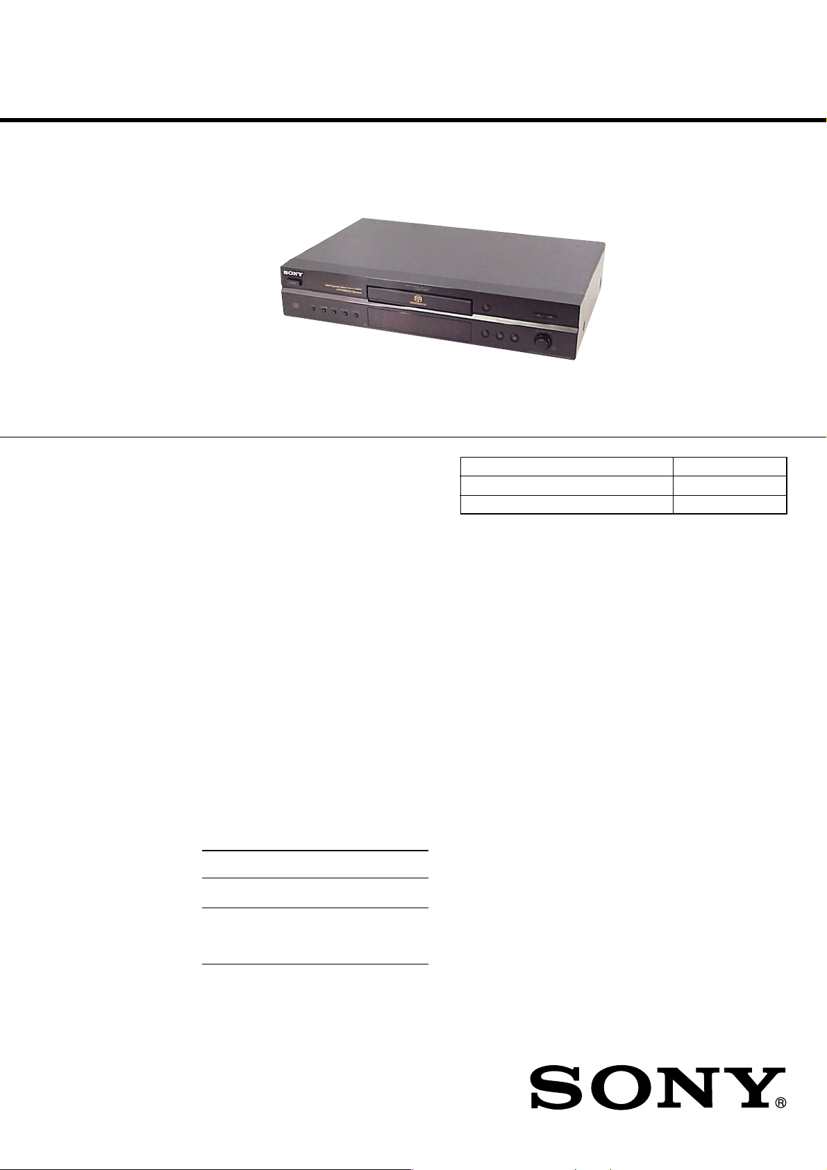
SCD-XE597
SERVICE MANUAL
Ver. 1.3 2006.02
SPECIFICATIONS
AEP Model
UK Model
Model Name Using Similar Mechanism NEW
CD Mechanism Type CDM66D-DVBU50
Optical Pick-up Name DBU-3
When a Super Audio CD is played
Playing frequency range 2 Hz to 100 kHz
Frequency response 2 Hz to 40 kHz (–3 dB)
Dynamic range 100 dB or more
Total harmonic distortion rat e
Wow and flutter Value of measurable limit
When a CD is played
Frequency response 2 Hz to 20 kHz
Dynamic range 96 dB or more
Total harmonic distortion rat e
Wow and flutter Value of measurable limit
Output connector
Jack type Output
ANALOG
5.1CH OUT
DIGITAL
(CD) OUT
OPTICAL*
*Output only the audio signals of the CD
Phono
jacks
Square
optical
output
connector
0.0035 % or less
(±0.001 % W. PEAK) or
less
0.0039 % or less
(±0.001 % W. PEAK) or
less
level
2 Vrms (at
50 kilohms)
–18 dBm (Light
Load
impedance
Over 10
kilohms
emitting
wave length:
660 nm)
General
Laser Semiconductor laser
Power requirements 230 V AC, 50/60 Hz
Power consumption 15 W
Dimensions (w/h/d) 430 95 283 mm incl.
Mass (approx.) 3.1 kg
Supplied accessories
Audio connecting cord Red and White 2 (1)
Remote commander RM-SX800 (1)
Battery R6 (size-AA) (2)
Design and specifications are subject to change
without notice.
(Super Audio CD: λ = 650
nm) (CD: λ = 780 nm)
Emission duration:
continuous
××
projecting parts
×
9-879-005-04
2006B16-1
© 2006.02
SUPER AUDIO CD PLAYER
Sony Corporation
Home Audio Division
Published by Sony Techno Create Corporation
SCD-XE597
TABLE OF CONTENTS
1. SERVICING NOTES ................................................ 3
2. GENERAL ................................................................... 4
3. DISASSEMBLY
3-1. Disassembly Flow ........................................................... 6
3-2. Cover ............................................................................... 6
3-3. MAIN Board.................................................................... 7
3-4. Loading Panel..................................................................7
3-5. Front Panel Section ......................................................... 8
3-6. KEY Board, DISPLAY Board ......................................... 8
3-7. CD Mechanism Deck (CDM66D-DVBU50) .................. 9
3-8. Base Unit (DVBU50) ...................................................... 9
3-9. RF Board, Pick-up Unit (DBU-3) ................................... 10
3-10. Belt (LD), LOADING Board, Motor (L) Assy................ 10
4. DIAGRAMS
4-1. Block Diagram ................................................................ 12
4-2. Printed Wiring Board — RF Section — ......................... 13
4-3. Schematic Diagram — RF Section — ........................... 14
4-4. Printed Wiring Board — MAIN Section — ................... 15
4-5. Schematic Diagram — MAIN Section (1/4) — ............ 16
4-6. Schematic Diagram — MAIN Section (2/4) — ............ 17
4-7. Schematic Diagram — MAIN Section (3/4) — ............ 18
4-8. Schematic Diagram — MAIN Section (4/4) — ............ 19
4-9. Printed Wiring Board — DISPLAY Section — ............ 20
4-10. Schematic Diagram — DISPLAY Section — ................ 21
NOTES ON HANDLING THE OPTICAL PICK-UP
BLOCK OR BASE UNIT
The laser diode in the optical pick-up block may suffer electrostatic
break-down because of the potential difference generated by the
charged electrostatic load, etc. on clothing and the human body.
During repair, pay attention to electrostatic break-down and also
use the procedure in the printed matter which is included in the
repair parts.
The flexible board is easily damaged and should be handled with
care.
NOTES ON LASER DIODE EMISSION CHECK
The laser beam on this model is concentrated so as to be focused on
the disc reflective surface by the objective lens in the optical pickup block. Therefore, when checking the laser diode emission,
observe from more than 30 cm away from the objective lens.
CAUTION
Use of controls or adjustments or performance of procedures
other than those specified herein may result in hazardous radiation
exposure.
This appliance is
classified as a CLASS 1
LASER product. This
label is located on the
rear exterior.
5. TEST MODE ............................................................... 22
6. EXPLODED VIEWS
6-1. Main Section.................................................................... 23
6-2. Front Panel Section ......................................................... 24
6-3. CD Mechanism Deck ...................................................... 25
6-4. Base Unit (DVBU50) ...................................................... 26
7. ELECTRICAL PARTS LIST................................27
LASER DIODE AND FOCUS SEARCH OPERATION
CHECK
Carry out the “S curve check” in “CD section adjustment” and check
that the S curve waveform is output three times.
Notes on chip component replacement
• Never reuse a disconnected chip component.
• Notice that the minus side of a tantalum capacitor may be
damaged by heat.
Flexible Circuit Board Repairing
• Keep the temperature of the soldering iron around 270 °C
during repairing.
• Do not touch the soldering iron on the same conductor of the
circuit board (within 3 times).
• Be careful not to apply force on the conductor when soldering
or unsoldering.
SAFETY-RELATED COMPONENT WARNING!!
COMPONENTS IDENTIFIED BY MARK 0 OR DOTTED LINE
WITH MARK 0 ON THE SCHEMATIC DIAGRAMS AND IN
THE PARTS LIST ARE CRITICAL TO SAFE OPERATION.
REPLACE THESE COMPONENTS WITH SONY PARTS WHOSE
PART NUMBERS APPEAR AS SHOWN IN THIS MANUAL OR
IN SUPPLEMENTS PUBLISHED BY SONY.
2
SECTION 1
SERVICING NOTES
SCD-XE597
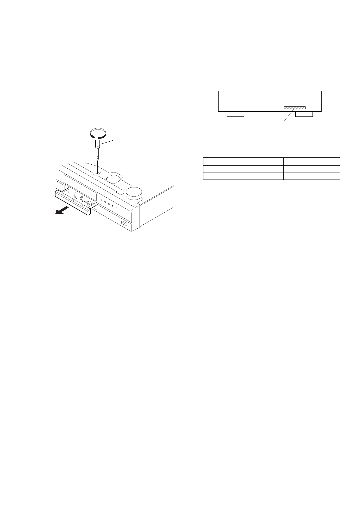
HOW TO OPEN THE DISC TRAY WHEN POWER SWITCH
TURNS OFF
Insert a tapering driver into the aperture of the unit bottom, and turn
in the direction of arrow.
Use a flat (-) head screwdriver to open the disc tray by manual
operation. (Flat head screwdriver with nominal blade length of
3mm.)
* To close the disc table, turn the driver in the reverse direction.
tapering driver
MODEL IDENTIFICATION
– Back Panel –
Parts No.
MODEL Part No.
AEP Model 4-255-245-0[ ]
UK Model 4-255-245-1[ ]
3
SCD-XE597
9q
q
q
q
q
q
q
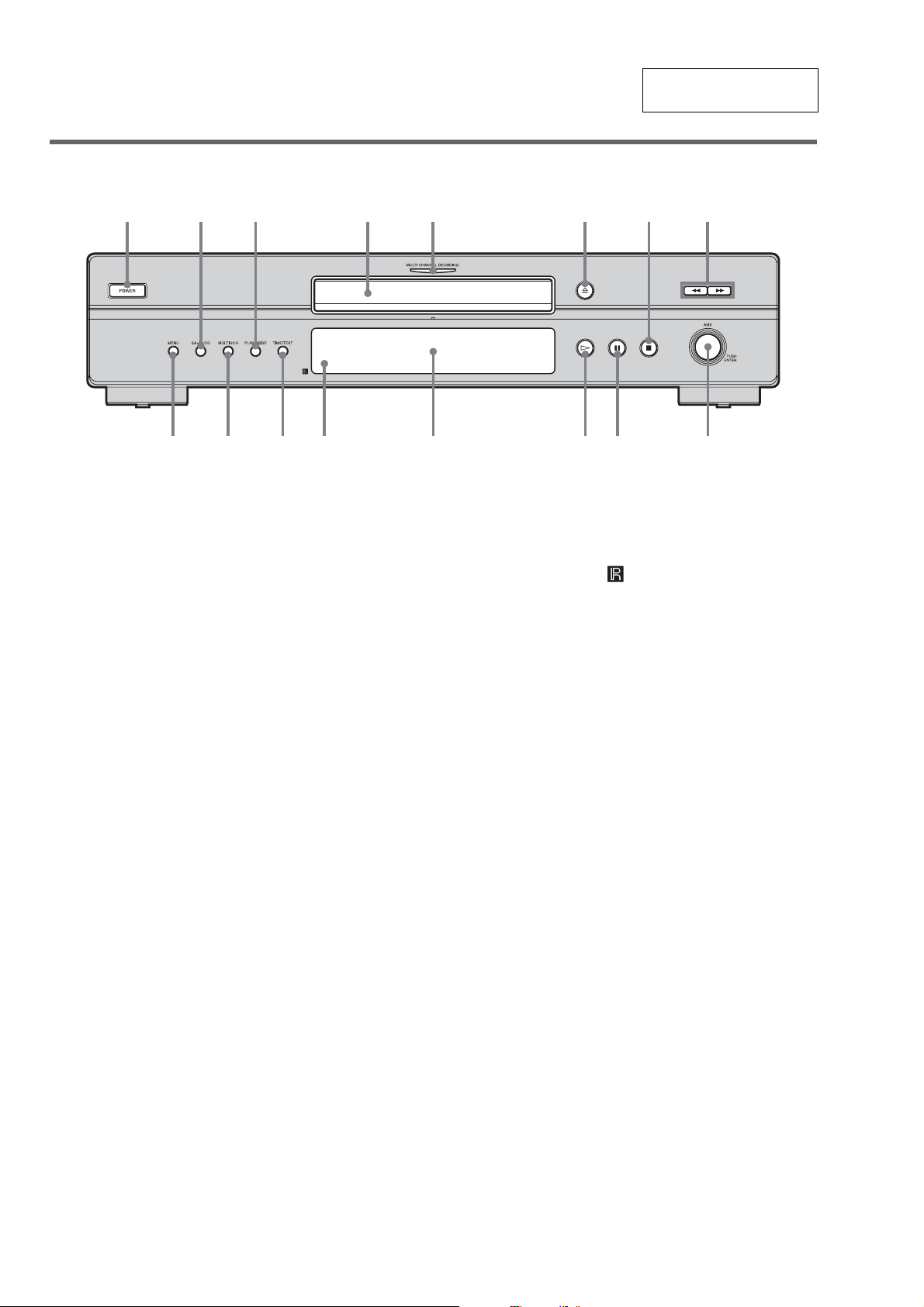
Front Panel
123 45 678
SECTION 2
GENERAL
d
h
g
f
s
a
This section is extracted
from instruction manual.
lL
;
A POWER switch (9)
B SA-CD/CD button (5, 9)
Each time you press the button while playing back
a hybrid disc, the layer to be played back switches
between the SA - CD layer and the CD la yer.
C PLAY MODE button (13, 14)
Press to select the pl ay mo de .
D Disc tray (9)
E MULTI CHANNEL DECODING indicator
Turns on when you turn on the player, or when the
Multi-channel Super Audio CD is loaded and
select the multi-channel playback area by pressing
MULTI/2CH.
F A button (9)
G x button (9, 14)
H m/M buttons (12)
I l AMS L dial
(AMS: Automatic Music Sensor) (8, 9, 10,
12, 14, 15, 16, 18)
J X button (9)
K H button (9, 12, 13, 14)
L Display window (10)
M Remote sensor (6)
N TIME/TEXT button (11)
Each time you press the button, the playing time of
the track, the remaining time of the disc, or TEXT
information appea r s in the display.
O MULTI/2CH button (5, 9)
Press to select the playback area when a disc with
the 2 channel area and the multi-channel area
(page 5) is loaded.
P MENU button (8, 9, 10, 12, 15, 16, 18)
Press to enter the menu.
Press to exit from the menu and return to the
normal display.
4
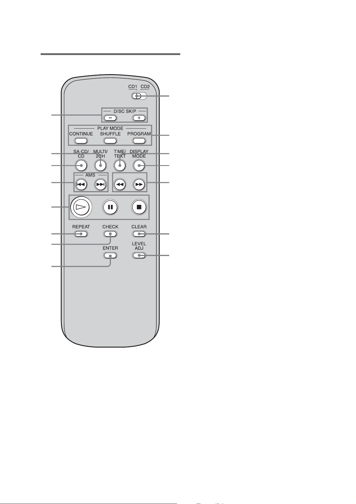
Remote
A CD1/ 2 (command mode ) switch (8)
Select the comman d mod e.
B CONTINUE button (13, 14)
Press to resume Continuous Play from Shuffle Play
or Program Play.
SHUFFLE button (13)
PROGRAM button (14)
C TI ME/TEXT button (11)
Each time you press the button, the playing time of
the track, the remaining time of the disc, or TEXT
information appe ars in the display.
D DISPLAY MODE button (12)
Press to turn the display information off or on.
E m/M buttons (12)
F CLEAR button (14)
Press to delete a progra me d tr a ck number.
G LEVEL ADJ button (17)
Press to adjust the output level balance for the
Multi-channel management fun ct ion ( pa g e 15).
H ENTER button (8, 9, 10, 12, 14, 15, 17, 18)
I CHECK button (14)
Press to check the programed order.
J REPEAT button (13)
K H button (9, 12, 13, 14)
X button (9)
x button (9, 14)
L AMS ./> buttons
(AMS: Automatic Music Sensor) (8, 9, 10,
12, 14, 15, 17, 18)
M SA-CD/CD button (5, 9)
Each time you press the button while playing back
a hybrid disc, the layer to be played back switches
between the SA-CD layer and the CD layer.
N MUL TI/2CH button (5, 9)
Press to select the playback area when a disc with
the 2 channel area and the multi-channel area
(page 5) is loaded.
O DI SC SKIP +/– buttons*
Press to select the disc .
*This button cannot be used in this player.
qg
qf
qd
qs
qa
q;
9
8
1
2
3
4
5
6
7
SCD-XE597
5
SCD-XE597
s
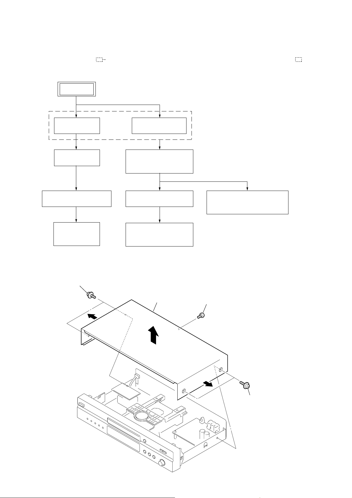
•This set can be disassembled in the order shown below.
•The dotted square with arrow (
completed.
3-1. DISASSEMBLY FLOW
SET
) prompts you to move to the next job when all of the works within the dotted square ( ) are
SECTION 3
DISASSEMBLY
3-2.COVER
(Page 6)
3-3.MAIN BOARD
(Page 7)
3-5. FRONT PANEL SECTION
(Page 8)
3-6.KEY BOARD,
DISPLAY BOARD
(Page 8)
Note: Follow the disassembly procedure in the numerical order given.
3-4.LOADING PANEL
3-7.CD MECHANISM DECK
(CDM66D-DVBU50)
3-8.BASE UNIT (DVBU50)
3-9. RF BOARD,
PICK-UP UNIT (DBU-3)
3-2. COVER
1
two screws
(case 3)
(Page 7)
(Page 9)
(Page 9)
(Page 10)
cover
3
screw
(+BVTP 3
3-10. BELT (LD), LOADING BOARD,
MOTOR (L) ASSY
(Page 10)
×
8)
4
5
4
2
two screw
(case 3)
6
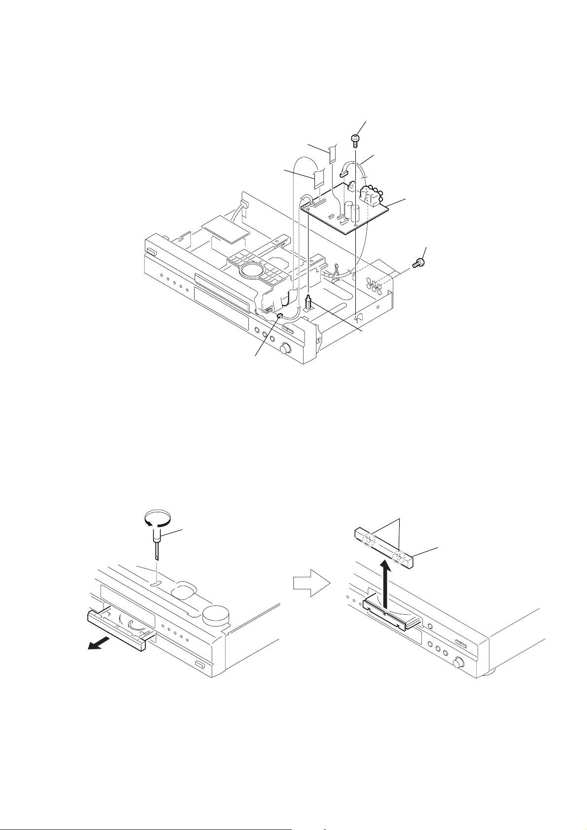
3-3. MAIN BOARD
)
3
wire (flat type)
(13 core) (CN703)
4
wire (flat type)
(31 core) (CN702)
6
screw
(+BVTP 3
2
×
8)
connector
(8p) (CN901)
8
MAIN board
5
three screws
(+BVTP 3
SCD-XE597
×
8
3-4. LOADING PANEL
1
1
tapering driver
connector
(5p) (CN151)
7
PWB holder
3
two claws
4
loading panel
2
7
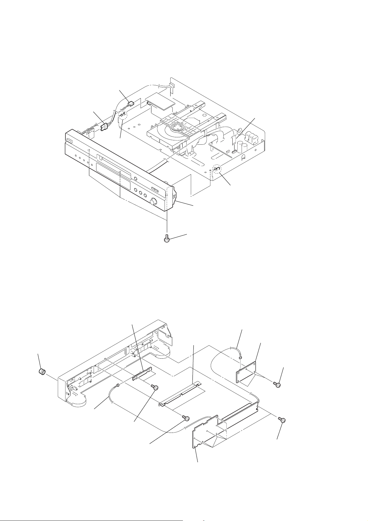
SCD-XE597
)
)
3-5. FRONT PANEL SECTION
3
connector (CN101)
2
connector (CN891)
4
claw
5
1
claw
wire (flat type)
(13 core) (CN703
3-6. KEY BOARD, DISPLAY BOARD
6
LED board
1
knob (AMS)
3
6
bracket
7
front panel section
three screws
(+BVTP 3 × 8)
8
connector (CN813)
9
KEY board
7
three screws
(+BVTP 2.6
×
8
5
connector (CN814)
4
two screws
(+BVTP 2.6
×
8)
2
two screws
(+BVTP 2.6
×
8)
qa
DISPLAY board
q;
seven screws
(+BVTP 2.6
×
8)
8
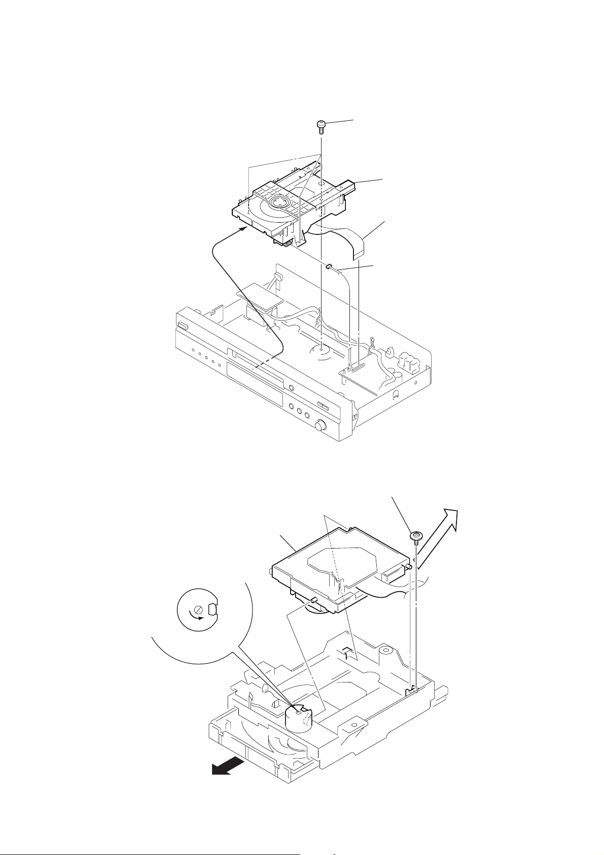
3-7. CD MECHANISM DECK (CDM66D-DVBU50)
k
3
three screws
(+BVTP 3
4
CD mechanism dec
(CDM66D-DVBU50)
1
wire (flat type)
(31 core) (CN702)
2
connector
(5p) (CN151)
SCD-XE597
×
8)
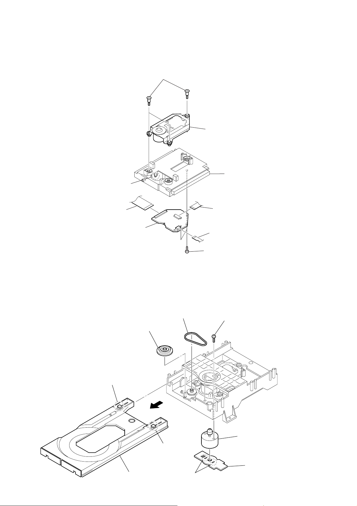
3-8. BASE UNIT (DVBU50)
1
Turn the cam to the direction of
arrow (counter clock wise) by
tapering driver.
DVBU50
3
screw (DIA. 12), floating
4
Remove the Base unit
(DVBU50) to the direction
of arrow.
2
Take off the tray.
9
SCD-XE597
)
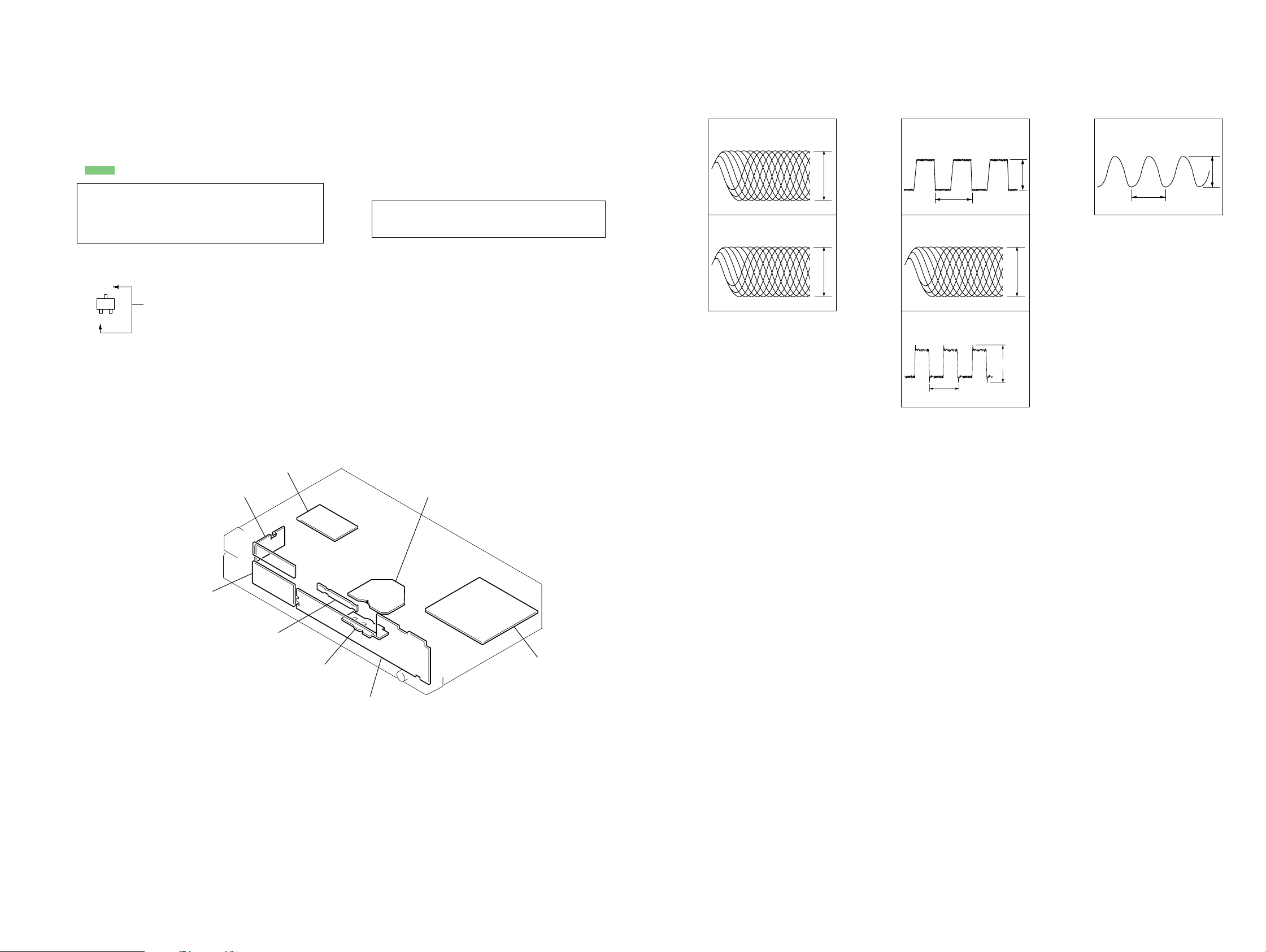
3-9. RF BOARD, PICK-UP UNIT (DBU-3)
2
hook
7
three screws
(step screw (M))
8
pick-up unit (DBU-3)
holder (66D)
5
wire (flat type) (CN002)
6
RF board
3-10. BELT (LD), LOADING BOARD, MOTOR (L) ASSY
5
gear (LD)
1
claw
6
belt (LD)
4
CN001
3
flexible board (
1
two screws
(BTTP M2.6)
7
CN003
two screws
×
4)
(B 2.6
10
4
tray (66)
3
2
claw
8
Removal the solders.
0
motor (L) assy
9
LOADING board
SECTION 4
d
DIAGRAMS
SCD-XE597
NOTE FOR PRINTED WIRING BOARDS AND SCHEMATIC DIAGRAMS
Note on Printed Wiring Board:
• X : parts extracted from the component side.
• Y : parts extracted from the conductor side.
• W : indicates side identified with part number.
• f : internal component.
• : Pattern from the side which enables seeing.
Caution:
Pattern face side: Parts on the pattern face side seen from
(Side B) the pattern face are indicated.
Parts face side: Parts on the parts face side seen from
(Side A) the parts face are indicated.
• Indication of transistor.
C
Q
B
E
These are omitted.
Note Schematic Diagrams.
• All capacitors are in µF unless otherwise noted. (p: pF)
50 WV or less are not indicated except f or electrolytics and
tantalums.
• All resistors are in Ω and 1/
specified.
• f : internal component.
• C : panel designation.
Note: The components identified by mark 0 or dotted
line with mark 0 are critical for safety.
Replace only with part number specified.
• A : B+ Line.
• B : B– Line.
•Voltages and waveforms are dc with respect to ground
under no-signal conditions.
no mark: SACD PLAY
( ): CD PLAY
•Voltages are taken with a VOM (Input impedance 10 MΩ).
Voltage variations may be noted due to normal production
tolerances.
•Waveforms are taken with a oscilloscope.
Voltage variations may be noted due to normal production
tolerances.
• Circled numbers refer to waveforms.
• Signal path.
J : CD
c : CD DIGITAL OUT (OPTICAL)
4
W or less unless otherwise
•Waveforms
– RF Board –
1 IC001 tl SIGO (CD)
200 ns/DIV
1 IC001 tl
40 ns/DIV
1.4 Vp-p
SIGO (SACD)
1.4 Vp-p
– MAIN Board – – DISPLAY Board –
2 IC706 uk DSPHREFO
354 ns
3 IC706 <z./
40 ns/DIV
3.5 Vp-p
RF IN (SACD)
1.4 Vp-p
5 IC801 5 IC
200 ns
4 IC320 2,4,6,q;,qs
3.3 Vp-p
88.6 ns
3.5 Vp-p
• Circuit Boards Location
POWER SW board
KEY board
PT board
LED board
LOADING board
RF board
MAIN boar
DISPLAY board
SCD-XE597
1111
 Loading...