

Sony SA-WP5000, SS-CNP5000, SS-MSP5000, SS-SRP5000 Service Manual
SA-WP5000/SS-CNP5000/CRP5000/
CRP7001/MSP5000/SRP5000
Q
Q
3
7
6
3
1
5
1
5
0
SERVICE MANUAL
Ver. 1.1 2008.05
TEL 13942296513 QQ 376315150 892498299
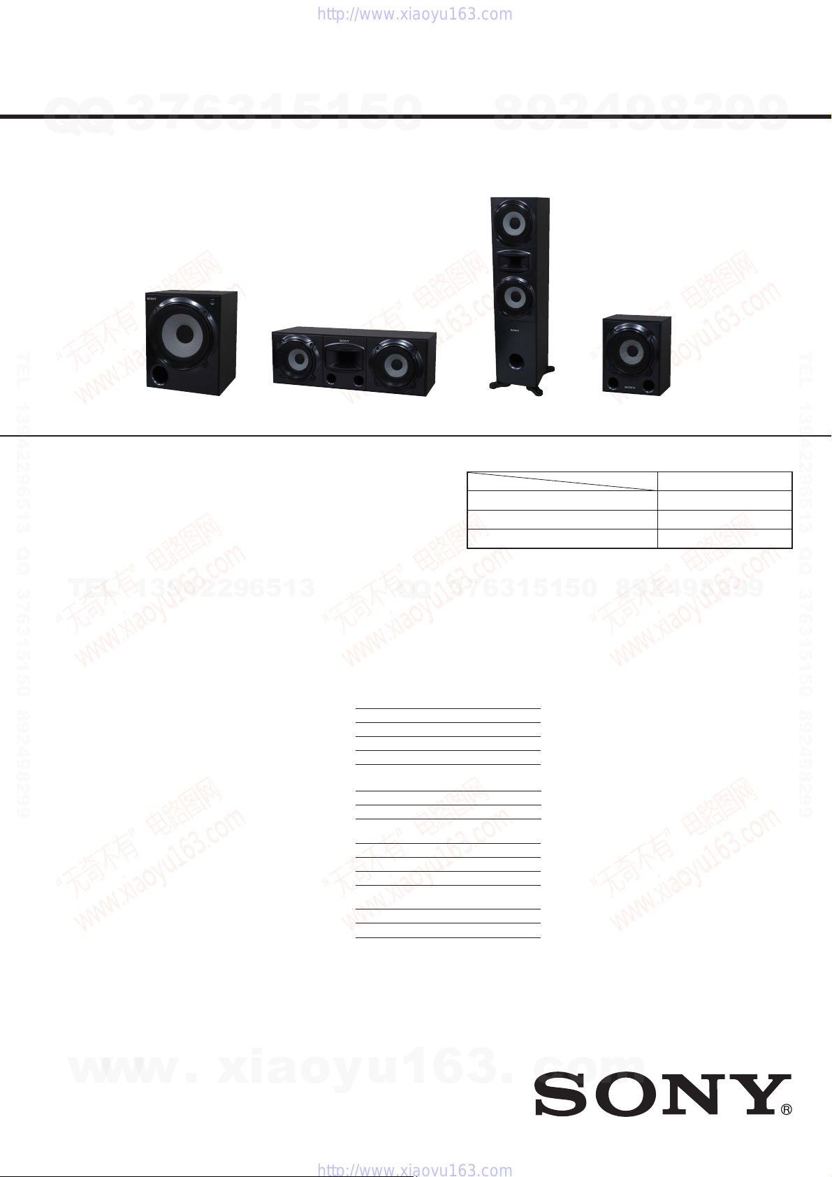
Photo: SA-WP5000 Photo: SS-CNP5000 Photo: SS-MSP5000 Photo: SS-SRP5000
• SA-WP5000 is the active subwoofer in HT-DDW5000/DDW7000.
• SS-CNP5000 is the center speaker in HT-DDW5000/DDW7000.
• SS-MSP5000 is the front speaker in HT-DDW5000/DDW7000.
• SS-SRP5000 is the surround/surround back speaker in HT-DDW5000/
DDW7000.
• SS-CRP5000/CRP7001 are composed of SS-CNP5000, SS-MSP5000
and SS-SRP5000.
SS-CRP5000/CRP7001 COMPONENT MODEL NAME
Front speaker SS-MSP5000
Center speaker SS-CNP5000
Surround/Surround back speaker SS-SRP5000
8
9
2
4
9
8
2
9
E Model
Australian Model
SS-CRP5000/CRP7001
9
TEL 13942296513 QQ 376315150 892498299
TEL
Speaker section
13942296513
• Front speaker (SS-MSP5000)
Speaker system 2-way, 3-driver, Bass
Speaker unit
Woofer: 160 mm, cone type × 2
Tweeter: 25 mm, horn type
Rated Impedance 4 ohm
Dimensions (width/height/depth) (Approx.)
Mass (Approx.) 13.5 kg
• Center speaker (SS-CNP5000)
Speaker system 2-way, 3-driver, Bass
Speaker unit
Woofer: 100 mm, cone type × 2
Tweeter: 25 mm, horn type
Rated Impedance 4 ohm
Dimensions (width/height/depth) (Approx.)
Mass (Approx.) 4.8 kg
• Surround/Surround back speaker
(SS-SRP5000)
Speaker system Full range, Bass reflex
Speaker unit
Woofer: 100 mm, cone type
Rated Impedance 4 ohm
Dimensions (width/height/depth) (Approx.)
Mass (Approx.) 1.4 kg
reflex, Magnetically
shielded
305 × 1,000 × 325 mm
(with foot)
reflex, Magnetically
shielded
515 × 175 × 225 mm
(with foot)
174 × 220 × 166 mm
(with foot)
SPECIFICATIONS
• Subwoofer (SA-WP5000)
Speaker system Active subwoofer, Bass
Speaker unit 250 mm, cone type
RMS output 200 W
Input LINE IN (input pin jacks)
5)
Measured under the following conditions:
Area code Power requirements
E51, SP, MY, AUS 240 V AC, 50 Hz
MX 127 V AC, 60 Hz
AR, TH 230 V AC, 50 Hz
6)
Measured under the following conditions:
Area code Power requirements
AR, TH 220 V AC, 50 Hz
Power requirements
Area code Power requirements
SP, MY 230 – 240 V AC, 50/60 Hz
MX 127VAC,60Hz
E51 120/220/240 V AC,
AR, TH 220 – 230 V AC, 50/60 Hz
AUS 240 V AC, 50 Hz
Q
Q
7
3
reflex, Magnetically
shielded
5)
6)
175 W
50/60 Hz
6
3
1
5
Power consumption 80 W
0
5
1
Dimensions (width/height/depth) (Approx.)
Mass (Approx.) 11 kg
Design and specifications are subject to
change without notice.
• Abbreviation
AR : Argentina model
AUS : Australian model
E51 : Chilean and Peruvian models
MX : Mexican model
MY : Malaysia model
SP : Singapore model
TH : Thai model
8
9
2
8
9
4
335 × 420 × 430 mm
(with foot)
2
9
9
SA-WP5000
ACTIVE SUBWOOFER
SS-CNP5000/MSP5000/SRP5000
SPEAKER SYSTEM
w
w
9-889-038-02
2008E05-1
©
w
2008.05
.
xia
Sony Corporation
Audio Business Group
Published by Sony Techno Create Corporation
o
y
u
1
6
3
.
c
o
m
SA-WP5000/SS-CNP5000/CRP5000/CRP7001/MSP5000/SRP5000
Notes on chip component replacement
• Never reuse a disconnected chip component.
Q
Q
• Notice that the minus side of a tantalum capacitor may be damaged by heat.
UNLEADED SOLDER
Boards requiring use of unleaded solder are printed with the leadfree mark (LF) indicating the solder contains no lead.
(Caution: Some printed circuit boards may not come printed with
the lead free mark due to their particular size)
: LEAD FREE MARK
Unleaded solder has the following characteristics.
• Unleaded solder melts at a temperature about 40 °C higher
than ordinary solder.
Ordinary soldering irons can be used but the iron tip has to be
TEL 13942296513 QQ 376315150 892498299
applied to the solder joint for a slightly longer time.
Soldering irons using a temperature regulator should be set to
about 350 °C.
Caution: The printed pattern (copper foil) may peel away if the
heated tip is applied for too long, so be careful!
• Strong viscosity
Unleaded solder is more viscous (sticky, less prone to fl ow)
than ordinary solder so use caution not to let solder bridges
occur such as on IC pins, etc.
• Usable with ordinary solder
It is best to use only unleaded solder but unleaded solder may
also be added to ordinary solder.
3
7
6
3
1
5
1
5
0
8
9
2
4
9
8
2
9
9
TEL 13942296513 QQ 376315150 892498299
• JIG
When disassembling the set, use the following jig (for speaker
removal).
Part No.: J-2501-238-A
TEL
JIG FOR SPEAKER REMOVAL
13942296513
Q
Q
3
7
6
3
1
5
1
5
0
8
9
2
4
9
8
2
9
9
SAFETY-RELATED COMPONET WARNING!
COMPONENTS IDENTIFIED BY MARK 0 OR DOTTED LINE
WITH MARK 0 ON THE SCHEMATIC DIAGRAMS AND IN
THE PARTS LIST ARE CRITICAL TO SAFE OPERATION.
w
w
REPLACE THESE COMPONENTS WITH SONY PARTS
WHOSE PART NUMBERS APPEAR AS SHOWN IN THIS
MANUAL OR IN SUPPLEMENTS PUBLISHED BY SONY.
2
w
.
xia
o
y
u
1
6
3
.
c
o
m
Q
SA-WP5000/SS-CNP5000/CRP5000/CRP7001/MSP5000/SRP5000
Note: Follow the disassembly procedure in the numerical order given.
7
Q
3
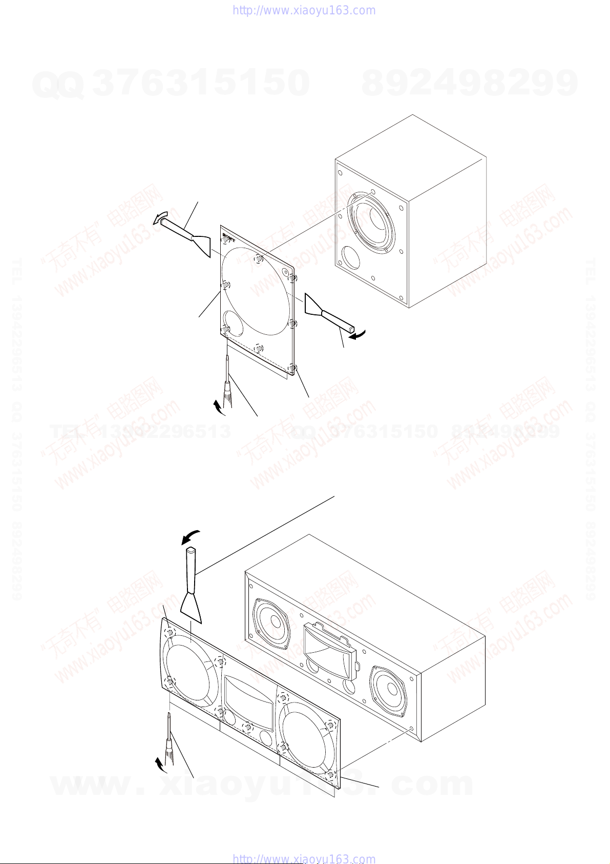
1-1. FRONT PANEL ASSY (SA-WP5000)
6
and raise the front panel assy gradually.
Note: When using a jig, please work so as not
to injure front panel and speaker cabinet.
1
5
1
3
Insert the jig (J-2501-238-A) into a space
5
SECTION 1
DISASSEMBLY
0
8
9
2
4
9
8
2
9
9
TEL 13942296513 QQ 376315150 892498299
front panel assy
Insert the jig (J-2501-238-A) into a space
and raise the front panel assy gradually.
Note: When using a jig, please work so as not
to injure front panel and speaker cabinet.
eight bosses
Insert a flat-tip screwdriver into a recess
TEL
13942296513
1-2. FRONT PANEL ASSY (SS-CNP5000)
in the bottom of the set
to raise the front panel assy a little.
Q
Q
7
3
Insert the jig (J-2501-238-A) into a space
and raise the front panel assy gradually.
Note 1: When using a jig, please work so as not
to injure front panel and speaker cabinet.
Note 2: Please insert jig from a gap on the front
panel assy underside and expand the
surrounding gap in turn.
6
3
1
5
1
5
0
8
9
2
4
9
8
2
9
TEL 13942296513 QQ 376315150 892498299
9
w
w
w
nine bosses
Insert a flat-tip screwdriver
.
xia
into a recess in the bottom of the set
to raise the front panel assy a little.
o
y
u
1
6
3
.
front panel assy
c
o
m
3
SA-WP5000/SS-CNP5000/CRP5000/CRP7001/MSP5000/SRP5000
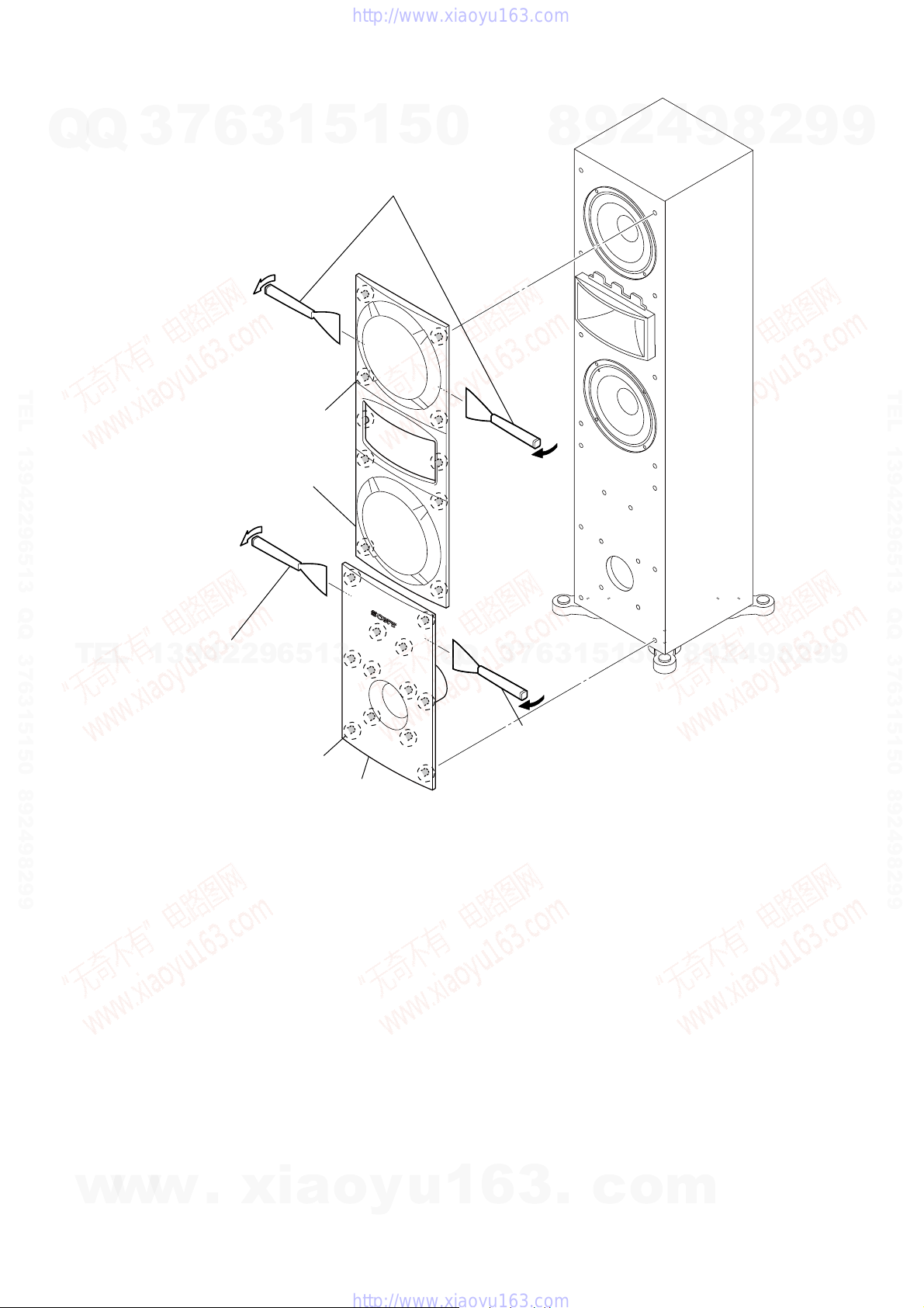
1-3. FRONT PANEL ASSY, DUCT PANEL ASSY (SS-MPS5000)
Q
Q
3
7
6
Insert the jig (J-2501-238-A) into a space
and raise the front panel assy gradually.
Note: When using a jig, please work so as not to injure
front panel and speaker cabinet.
3
1
5
1
5
0
8
9
2
4
9
8
2
9
9
TEL 13942296513 QQ 376315150 892498299
ten bosses
front panel assy
Insert the jig (J-2501-238-A) into a space
TEL
and raise the duct panel assy gradually.
Note: When using a jig, please work
so as not to injure duct panel assy
and speaker cabinet.
13942296513
twelve bosses
duct panel assy
Q
Q
7
3
and raise the duct panel assy gradually.
Note: When using a jig, please work
so as not to injure duct panel assy
and speaker cabinet.
4
2
9
8
0
5
1
5
1
3
6
Insert the jig (J-2501-238-A) into a space
9
8
2
9
TEL 13942296513 QQ 376315150 892498299
9
4
w
w
w
.
xia
o
y
u
1
6
3
.
c
o
m
SA-WP5000/SS-CNP5000/CRP5000/CRP7001/MSP5000/SRP5000
SA-WP5000/SS-CNP5000/CRP5000/CRP7001/MSP5000/SRP5000
55
SECTION 2
DIAGRAMS
For Schematic Diagrams.
Note:
• All capacitors are in μF unless otherwise noted. (p: pF) 50
WV or less are not indicated except for electrolytics and
tantalums.
• All resistors are in Ω and 1/4 W or less unless otherwise
specifi ed.
• 2 : nonfl ammable resistor.
• 5 : fusible resistor.
• C : panel designation.
THIS NOTE IS COMMON FOR PRINTED WIRING BOARDS AND SCHEMATIC DIAGRAMS.
(In addition to this, the necessary note is printed in each block.)
• A : B+ Line.
• B : B– Line.
• Voltages and waveforms are dc with respect to ground
under no-signal conditions.
no mark : Power on
• Voltages are taken with VOM (Input impedance 10 MΩ).
Voltage variations may be noted due to normal production
tolerances.
• Signal path.
F : AUDIO
• Abbreviation
AR :
Argentina model
AUS : Australian model
E51 : Chilean and Peruvian models
MX : Mexican model
MY : Malaysia model
SP : Singapore model
TH : Thai model
For Printed Wiring Boards.
Note:
• X : Parts extracted from the component side.
• Y : parts extracted from the conductor side.
• : Pattern from the side which enables seeing.
(The other layers' patterns are not indicated.)
• Indication of transistor.
Note: The components identifi ed by mark 0 or dotted
line with mark 0 are critical for safety.
Replace only with part number specifi ed.
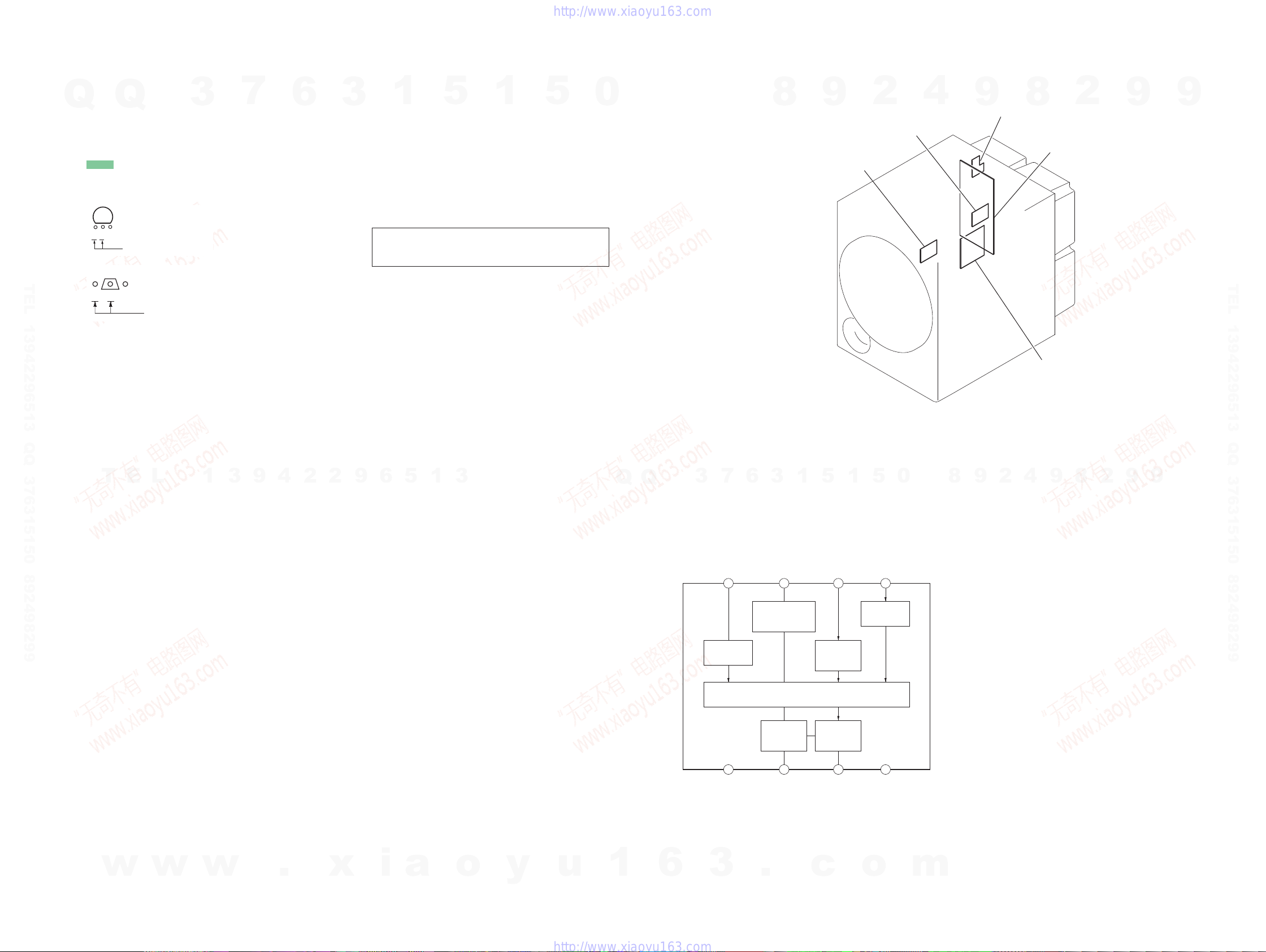
• Circuit Boards Location
– SA-WP5000 –
• IC Block Diagram
– MAIN Board (SA-WP5000) –
IC500 μPC1237C-A
Ver. 1.1
Q
TEL 13942296513 QQ 376315150 892498299
Q
CEB
These are omitted.
Q
B
CE
These are omitted.
3
7
6
3
1
5
1
5
0
8
9
LED board
2
SWITCH board
4
9
INPUT CONTROL board
8
MAIN board
POWER TRANS board
2
9
9
TEL 13942296513 QQ 376315150 892498299
T
E
L
1
3
9
4
2
2
9
6
5
1
3
Q
Q
1
3
6
7
3
OFF AC
4
AC-OFF
DETECTOR
5
GND
RESET
3
SWITCH FOR
LATCH/AUTOMATIC
RESET
FLIP-FLOP
OUTPUT
OFFSET
DETECTOR
6
RELAY
DRIVER
5
OUTPUT
OFFSET
DETECTOR
OUTPUT
OFFSET
DETECTOR
1
DETECT DC
2
7
OFF AC
5
LOADOVER
1
OVERLOAD
DETECTOR
8
VCC
0
8
9
2
4
9
8
2
9
9
w
w
w
.
x
i
a
o
y
u
1
6
3
.
c
o
m
 Loading...